Embed Size (px)
Citation preview

LYT5216-5228LYTSwitch-5 Family
www.power.com March 2016
Single-Stage LED Driver IC with Combined PFC and Constant Current Output in Isolated and Non-Isolated Topologies
This Product is Covered by Patents and/or Pending Patent Applications.
Product Highlights
Combined Single-Stage PFC + Accurate CC Output• Accurate CC, better than ±3%• Power Factor >0.9• Low THD, <10% with typical input and output conditions• >90% efficient in optimized designs• High switching frequency and DCM allow compact magnetics
Design Flexibility• Supports buck, buck-boost, tapped-buck, boost, isolated and
non-isolated flyback topologies• 2 MOSFET voltage options and 3 power levels for optimum device
selection
Highest Reliability• No electrolytic bulk capacitors or optoisolators for increased lifetime• Comprehensive protection features
• Input and output overvoltage• Open-loop protection
• Advanced thermal control• Thermal foldback allows output light delivery at abnormally high
ambient temperatures• Hysteretic shutdown provides protection during fault conditions
Description
The LYTSwitch™-5 family is ideal for single-stage power factor corrected constant current LED applications – bulbs, tubes and ballasts.
Each device incorporates a high-voltage power MOSFET and discon-tinuous mode, variable frequency, variable on-time controller. The controller also provides fast (cycle-by-cycle) current limit, input and output OVP, plus advanced thermal management circuitry.
The combination of a low-side switching topology, cooling via electroni-cally quiet SOURCE pins and frequency jitter ensures extremely low EMI. This reduces the size of the input filter components – greatly reducing audible noise.
The part numbers shown in Table 1 describe 3 different power levels and two MOSFET voltage options to cost-optimize designs, while EcoSmart™ switching technology ensures maximum efficiency for each device size and load condition.
Figure 1a. Typical Application Schematic: Isolated Flyback.
Figure 1b. Typical Application Schematic: Non-Isolated Buck.
Output Power Table
Product2Output Power1
90-308 VAC
LYT5225D 9 W
LYT5216D, LYT5226D 16 W
LYT5218D, LYT5228D 25 W
Table 1. Output Power Table.Notes: 1. Maximum practical continuous power in an open frame design with adequate
heat sinking, measured at 50˚C ambient (see Key Applications Considerations for more information).
2. Package: D: SO-16B.
Figure 2. SO-16B (D Package).
PI-7711-121015
LYTSwitch-5
DS
L D
DO
OC SFB BP
CONTROL
PI-7799-121015
LYTSwitch-5
DS
L D
DO
OC SFB BP
CONTROL

Rev. C 03/16
2
LYT5216-5228
www.power.com
Figure 3. Block Diagram.
AUTO-RESTART
FREQUENCY AND DUTY CYCLE CONTROL
MULTIPLIER
FAULTHANDLING
PI-7753-110215
FEEDBACK(FB)
DRIVER CURRENTSENSING
(DS)
OUTPUTCOMPENSATION
(OC)
SOURCE(S)DATA
OUTPUT(DO)
VFB(AR)
VFB
IFB
UPDATE
S
R
Q
Q
+
BYPASS(BP)
Enable(EN)
DRAIN(D)
LINE-SENSE(L)
VFB
VFB(SK)
4.7 V
ILIM
VLOV
ILIM
V_ILIM
VZC
UV
SOA
REGULATOR5.25 V
+
LOV
ZC
LOV
CURRENT LIMITSOA S
R
Q
QUV

Rev. C 03/16
3
LYT5216-5228
www.power.com
Pin Functional Description
LINE SENSE (L) PinThe LINE-SENSE pin measures input voltage. Input OVP is activated when LINE-SENSE pin current exceeds the predetermined threshold.
DATA OUTPUT (DO) PinDescribes auto-restart events.
DRIVER CURRENT SENSE (DS) PinDRIVER CURRENT SENSE pin senses the driver current. This current is used to deduce output current: it is multiplied by the input voltage and the result is then divided by the output voltage to obtain output current.
RDS (W) Topology
6 k – 12 K Buck, Buck-Boost, Isolated Flyback
24 k Non-Isolated Flyback
Table 2. Topology Selection Resistor.
FEEDBACK (FB) PinIn normal operation the preset threshold on the FEEDBACK pin is 300 mV.
Cycle skipping is triggered when voltage on this pin exceeds 600 mV.Auto-Restart is triggered when voltage on this pin exceeds 2 V.
BYPASS (BP) Pin5.25 V supply rail.
Figure 4. Pin Configuration.
PI-7712-091015
D Package (SO-16B)
OC16
BP15
S14
S13
S12
S11
S10
S9
8D
5NC
4DS
3DO
2L
1FB
OUTPUT COMPENSATION (OC) PinOutput OVP for all topologies. Output voltage compensation for indirect output current sense topologies.
DRAIN (D) PinHigh-voltage internal MOSFET (725 V or 650 V).
SOURCE (S) Pin:Power and signal ground.

Rev. C 03/16
4
LYT5216-5228
www.power.com
Applications Example
12 W Tube Lamp Driver Accurate Regulation, High Power Factor, Low ATHD Design Example (DER-515)
The circuit shown in Figure 5 is configured as a buck-boost power supply utilizing the LYT5526D from the LYTSwitch-5 family of ICs. This type of LED driver configuration is common for tube lamp applications where accurate regulation, high efficiency, high power factor and low ATHD are required along with low component count for high reliability. The output can drive an LED load from 70 V to 80 V with a constant output current of 160 mA ±3% across input range of 90 VAC to 308 VAC and can operate in a maximum ambient tempera-ture of 100 ºC with good margin below the thermal foldback protection point. It has an efficiency of greater than 89%, very low ATHD% (less than 10%) and high power factor of greater than 0.95 measured at nominal input voltages (115 VAC and 230 VAC).
LYTSwitch-5 also can be configured in a buck topology, and has advantages where low ATHD is not a critical requirement. Buck designs can realize between 15% to 33% ATHD. Advantages of buck over buck-boost configuration are:
• Lower stress voltage on the driver MOSFET.• Higher system efficiency.• Potentially smaller EMI filter – dependent on power, shape and size
of system.
Circuit Description The LYTSwitch-5 device (U1- LYT5526D) combines a high-voltage power MOSFET, variable frequency and on-time control engine, fast start-up, and protection functions including line and output over-
voltage into a single package, greatly reducing component count. The integrated 725 V power MOSFET provides a large drain voltage margin in universal input AC applications thus increasing reliability. A 625 V MOSFET option is also offered to reduce cost in applications where the voltage stress on the MOSFET is lower. Configured to operate as a discontinuous conduction mode buck-boost converter, U1 provides high power factor and very low ATHD via its internal control algorithm (the design also features low input capacitance to further reduce THD and increase PF). Discontinuous conduction mode inherently eliminates reverse current from the output diode when the MOSFET is in the off-state reducing high frequency noise and allowing the use of a simpler, smaller EMI filter which also improves efficiency.
Input FilterAC input power is rectified by bridge BR1. 1000 V voltage rating is recommended (the maximum clamp voltage for a typical 320 V varistor is 850 V). The rectified DC is filtered by the input capacitors C1 and C2. Too much capacitance degrades power factor and ATHD, so the values of the input capacitors were adjusted to the minimum values necessary to meet EMI with a suitable margin. Inductor L1, C1 and C2 form a π (pi) filter, which attenuates conducted differential and common mode EMI currents. Resistor R1 across L1 damps the Q of the filter inductor to improve filtering without reducing low frequency attenuation. F1 provides input protection against catastrophic failure such as short-circuit after the fuse. For cost
DS
L D
DOOC SFB BP
CONTROL
R32 MΩ1%
R42 MΩ1%
LYTSwitch-5U1
LYT5226D
C2150 nF450 V
Optional RCD Clamp
C1100 nF450 V
R76.04 kΩ
1%
R86.04 kΩ
1%
R940.2 kΩ
1%
R5100 kΩ
1%
R66.2 kΩ
R103 Ω1%
C410 µF10 V
C6150 nF25 V
R2680 kΩ
L13.3 mH
BR1B10S-G1000 V
RV1320 VAC
90 - 308VAC
F15 AL
N
R110 kΩ
PI-7763-120315 HLBB
D7MURS160T3G
D5RS1K
C8100 µF100 V
C32.2 µF450 V
R11180 kΩ
75 V, 160 mA
RTN
T1EFD15
T1EFD15
C710 µF25 VC5
1 µF10 V
D6BAV21W-7-F
Figure 5. 12 W, 75 V, 160 mA Non-Isolated Tube Lamp Driver for Wide Input Range of 90 VAC to 308 VAC using LYT5526D.

Rev. C 03/16
5
LYT5216-5228
www.power.com
reduction, this can be replaced by a fusible resistor (typically a flame proof wire-wound type) which would need to be rated to withstand the instantaneous dissipation induced when charging the input capacitance when first connected to the input line.
Selection of fuse (F1) type and rating is dependent on input surge requirements. Typical minimum requirement for tube application is 500 V differential surges. This design meets a 3 kV surge specifica-tion, so a 5-ampere slow blow fuse was used. A fast-blow fuse with a high ampere energy (I2T) rating could also be used.
An optional RCD surge clamp circuit (D5, R2 and C3) can be employed for differential surge voltage requirement of 3 kV. Capacitor C3 can also be increased to help meet a higher surge voltage requirement.
LYTSwitch-5 Output RegulationIn order to maintain very accurate output current regulation – within ±3%, the FEEDBACK (FB) pin voltage (with an appropriately selected low-pass filter comprising R9 and C6) is compared to a preset average feedback voltage (VFB) of 300 mV. When the detected signal is above or below the preset average VFB threshold voltage, the onboard averaging-engine will adjust the frequency and/or on-time to maintain regulation.
The bias winding voltage is proportional to the output voltage (controlled by the turns-ratio between the bias supply and output-main winding). This allows the output voltage to be monitored without the need for output-side feedback components. Resistor R5 converts the bias voltage into a current which is fed into the OUTPUT COMPENSATION (OC) pin of U1. The OUTPUT COMPENSATION pin current is also used to detect output overvoltage which is set to 30% above the nominal output voltage. Once the current exceeds the ILOV+ threshold the IC will trigger a latch which disables switching which prevents the output from rising further. An AC recycle is needed to reset this protection mode once triggered.
In order to provide line input voltage information to U1 the rectified input AC voltage is fed into the LINE SENSE (L) pin of U1 as a current via R3 and R4 (4 MW total resistance). This sensed current is also used by U1 to detect input zero-crossing and set the input line overvoltage protection threshold. In a line overvoltage condition once this current exceeds the IOOV threshold, the IC will instanta-neously disable switching to protect the MOSFET from further voltage stress. The IC will start switching as soon the line voltage drops to safe levels indicated by the L pin current dropping by 5 mA.
The primary switched current is sensed via R10 and filtered with C4. The signal is fed into the DRIVER CURRENT SENSE (DS) pin. A low ESR ceramic capacitor of at least 10 mF is recommended for capacitor C4.
The internal frequency/on-time engine inside LYTSwitch-5 combines the OUTPUT COMPENSATION pin current, the LINE SENSE pin current and the DRIVER CURRENT SENSE pin current information to deduce the FB signal. This is compared to an internal VFB threshold to maintain accurate constant output current.
It is important to note that for accurate output current regulation the use of 1% tolerance for LINE SENSE pin resistors (R3 and R4) is recommended. This recommendation also applies to OUTPUT COMPENSATION pin resistor R5, FEEDBACK pin resistor R9 (capacitor C6 at least X7R type), and DRIVER CURRENT SENSE pin resistor R7 and R10.
Diode D6 and C7 provides a bias supply for U1 from an auxiliary winding on the transformer. Bias supply recommended voltage level is 12 V. Filter capacitor C7 should be sized to ensure a low ripple voltage. Capacitor C5 serves as local decoupling for the BYPASS pin of U1 which is the supply pin for the internal controller. Current via R6 is typically limited to 1 mA. During start-up, C5 is charged to ~5.25 V from an internal high-voltage current source internally fed from the DRAIN pin. This allows U1 to start switching. After start-up the operating supply current is provided from the bias supply via R6. The recommended value for the BYPASS pin capacitor C5 is 1 mF. The voltage rating for the capacitor should be greater than 7 V. The capacitor can be a ceramic or electrolytic type, but tolerance should be less than 50%. The capacitor must be physically located close to BYPASS and SOURCE pins for effective noise decoupling.
Output Rectification During the switching off-state the output from the transformer main winding is rectified by D7 and filtered by C8. An ultrafast 1 A, 600 V with 35 ns reverse recovery time (trr) diode was selected for efficiency. The value of the output capacitor C8 was selected to give peak-to-peak LED ripple current equal to 30% of the mean value. For designs where lower ripple is desirable the output capacitance value can be increased unlike traditional power supplies, low ESR capacitors are not required for the output stage of LED designs.
A small output pre-load resistor R11 discharges the output capacitor when the driver is turned off, giving a relatively quick and smooth decay of the LED light. Recommended pre-load power dissipation is ≤0.5% of the output power.
Key Design Considerations
Device SelectionThe data sheet power table (Table 1) represents the maximum practical continuous output power that can be delivered in an open frame design with adequate heat sinking.
DER-515 is a 12 W driver. The LYT5226D IC was chosen for its higher voltage MOSFET rating of 725 V because the topology chosen was a buck-boost and the specification called for a maximum input voltage of 308 VAC. In other applications where surge and line voltage conditions allow, it may be possible to use the 650 V MOSFET option to reduce design cost without impacting reliability.
Magnetics DesignThe core type selected was a low profile EFD15 with ferrite core material and a wide winding window that allowed better convection cooling for the winding.
Input Range Typical Line Surge Requirement Protection
90 to 264 VAC500 V Differential Surge /
2.5 kV Ring Wave275 VAC MOV
90 to 308 VAC1 kV to 3 kV Differential
Surge / 2.5 kV Ring Wave320 VAC MOV,
RCD Clamp
Table 3. Recommended Surge Protection.
Output Power Table
Product2Output Power1
90-308 VAC
LYT5225D 9 W
LYT5216D, LYT5226D 16 W
LYT5218D, LYT5228D 25 W
Table 4. Output Power Table.
Rev. C 03/16
6
LYT5216-5228
www.power.com
Figure 6. DER-515 PCB Layout Example using SO-16B D Package. Shows the Location of Critical Components and Loop Areas on the PCB Layout.
To ensure that discontinuous conduction mode (DCM) operation of LYTSwitch-5 is maintained over line input and inductance tolerance variations, and to ensure for accurate output current regulation, it is recommended that the LYTSwitch-5 PIXls spreadsheet located at PI Expert web lab (http://piexpertweblab.power.com/site/login) should be used for magnetics calculations.
EMI ConsiderationsTotal input capacitance affects PF and ATHD – increasing the value will degrade performance. With LYTSwitch-5, the combination of a low-side switching configuration and frequency jitter reduces EMI and enables the use of small and simple π (pi) filter. It also allows simple magnetic construction where the main winding can be wound continuously using the automated winding approach preferred for low-cost manufacturing. The recommended location of the EMI filter is after the bridge rectifier. This allows the use of regular film capacitors as opposed to more expensive safety rated X capacitors that would be required if the filter is placed before the bridge.
Surge Immunity ConsiderationThis design assumed a differential surge requirement of 3 kV which can be met easily with LYTSwitch-5 line overvoltage protection and using a RCD surge clamp circuit (D5, R2 and C3) and MOV (RV1). For lower differential surge requirement such as 1 kV, capacitor C3 can be reduced to 1 mF.
Thermal and Lifetime ConsiderationsLighting applications present thermal challenges to the driver. In many cases the LED load dissipation determines the working ambient temperature experienced by the drive. Thermal evaluation should be performed with the driver inside the final enclosure. Temperature has a direct impact on driver and LED lifetime. For every 10 °C rise in temperature, component life is reduced by a factor of 2. Therefore it is important to verify and optimize the operating temperatures of all components.
Quick Design Checklist
Maximum Drain VoltageVerify that the peak drain voltage stress (VDS) does not exceed maximum acceptable drain voltage under all operating conditions, including start-up and fault conditions.
Maximum Drain CurrentMeasure the peak drain current under all operation conditions (including start-up and fault conditions). Look for transformer saturation (usually occurs at highest operating ambient tempera-tures). Verify that the peak current is less than the stated Absolute Maximum Rating in the data sheet.
Thermal CheckAt maximum output power, for both minimum and maximum line voltage and maximum ambient temperature; verify that temperature specifications are not exceeded for the LYTSwitch-5, transformer, output diodes, output capacitors and clamp components.
PCB Layout Considerations
The EMI filter components should be located close together to improve filter effectiveness. Place the EMI filter components C1 and L1 as far away as possible from any switching nodes on the circuit board especially U1 drain node, output diode (D7) and the transformer (T1).
Care should be taken in placing the components on the layout that are used for processing input signals for the feedback loop – any high frequency noise coupled to the signal pins of U1 may affect proper system operation. The critical components in DER-515 are R5, R9, C6, R4, R7 and R8. It is highly recommended that these components be placed very close to the pins of U1 (to minimize long traces which could serve as antenna) and far away as much as possible from any high voltage and high current nodes in the circuit board to avoid noise coupling.
The bypass supply capacitor C5 should be placed directly across BYPASS pin and SOURCE pin of U1 for effective noise decoupling.
As shown in Figure 6, minimize the loop areas of the following switching circuit elements to lessen the creation of EMI.
• Loop area formed by the transformer output winding (T1), output rectifier diode (D7) and output capacitor (C8).
• Loop area formed by transformer bias winding (T1), rectifier diode (D6) and filter capacitor (C7).
• Loop area formed by input capacitor (C2), transformer (T1) main winding R10, C4 and internal MOSFET (U1).
Lastly, unlike discrete MOSFET designs where heat sinking is through the drain tab and which generates significant EMI, the LYTSwitch-5 devices employ low-side switching and the ground potential SOURCE pins are used for heat sinking. This allows the designer to maximize the copper area for good thermal management but without having the risk of increased EMI.
Design Tools
Up-to-date information on design tools can be found at the Power Integrations web site: www.power.com
LYTSwitch-5 PIXls spreadsheet is located at PI Expert web lab: http://piexpertweblab.power.com/site/login.
FEEDBACK Pin Resistor R9 and C6
LINE SENSE Pin Resistor R4
Drain CurrentSense R10 and C4
OUTPUT COMPENSATIONPin Resistor R5
BYPASS PinCapacitor C5
Bias Diode Rectifier D6and Filter C7
OutputCapacitor
TRF
DRIVER CURRENTSENSE Pin Resistor R7
DATA OUTPUT PinResistor R8
Ouput DiodeRectifier D7 and
Filter C8
PI-7795-120315

Rev. C 03/16
7
LYT5216-5228
www.power.com
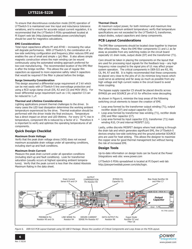
Absolute Maximum Ratings(1,3)
DRAIN Pin Voltage: LYT521x............................ -0.3 V to 650 V LYT522x ........................... -0.3 V to 725 VDRAIN Pin Peak Current(4) LYT5225 ........................... 1.95 A (3.16 A) LYT5216 ............................. 3.25 A (4.0 A) LYT5226 ........................... 2.64 A (4.35 A) LYT5218 ............................. 5.06 A (6.3 A) LYT5228 ........................... 4.16 A (6.86 A)BP, DO, DS, OC, L DS, FB Pin Voltage ..........................-0.3 V to 6.5 VLead Temperature(2) .............................................................. 260 °CStorage Temperature ...................................................-65 to 150 °COperating Junction Temperature .................................. -40 to 150 °C
Notes:1. All voltages referenced to Source, TA = 25 °C.2. 1/16 in. from case for 5 seconds.3. The Absolute Maximum Ratings specified may be applied, one at a
time without causing permanent damage to the product. Exposure to Absolute Maximum Ratings for extended periods of time may affect product reliability.
4. The higher peak Drain current (in parentheses) is allowed while the Drain voltage is simultaneously less than 400 V for 725 V integrated MOSFET version, or less than 325 V for 650 V integrated MOSFET version.
Parameter Symbol
Conditions SOURCE = 0 V
TJ = -40 °C to +125 °C (Unless Otherwise Specified)
Min Typ Max Units
Control Functions
MaximumOutput Frequency fMAX TJ = 25 °C
Average 115.3 124 132.7 kHz
Peak-to-Peak Jitter 8 %
MinimumOutput Frequency fMIN TJ = 0 °C to 125 °C
Average 40 kHz
Peak-to-Peak Jitter 8 %
Frequency Jitter Modulation Rate fM See Note A 1.76 kHz
Maximum On-Time TON(MAX) TJ = 25 °C 5.75 6.25 6.75 ms
Minimum On-Time TON(MIN) TJ = 25 °C 0.95 1.05 1.15 ms
FEEDBACK Pin Voltage VFB TJ = 25 °C 291 300 309 mV
FEEDBACK Pin Voltage Triggering Cycle Skipping
VFB(SK) 600 mV
FEEDBACK Pin Overvoltage Threshold VFB(OV) 2000 mV
Feedback Pull-Up Current IFB -1.3 -1.0 -0.7 mA
Thermal Resistance
Thermal Resistance: SO-16B Package: (qJA) ..................................................78 °C/W(2) (qJA) .................................................... 68 °C/W(3)
(qJC)(1) ...............................................43 °C/W
Notes:1. Measured per JESD 51-1, MIL-STD-883C-1012.1 and SEMI test
method #G43-87.2. Soldered to 0.36 sq. inch (232 mm2) 2 oz. (610 g/m2) copper clad,
with no external heat sink attached.3. Soldered to 1 sq. in. (645 mm2), 2 oz, (610 g/m2) copper clad.
Rev. C 03/16
8
LYT5216-5228
www.power.com
Circuit Protection
Current Limit ILIMIT
di/dt = 974 mA/ms TJ = 25 °C
LYT5225 1232 1325 1418
mAdi/dt = 1403 mA/ms
TJ = 25 °CLYT52x6 1767 1900 2033
di/dt = 2239 mA/ms TJ = 25 °C
LYT52x8 2860 3075 3290
Leading Edge Blanking Time tLEB TJ = 25 °C 130 165 ns
Current Limit Delay TILD
TJ = 25 °CSee Note A
160 ns
Thermal Foldback Temperature TFB See Note A 138 142 146 °C
Thermal Shutdown Temperature TSD See Note A 155 160 165 °C
Thermal Shutdown Hysteresis TSD(H) See Note A 75 °C
SOA Switch ON-Time TON(SOA) TJ = 25 °C 610 690 ns
Auto-Restart Current Threshold for Output Undervoltage
IOUV TJ = 25 °C 40 52 58 mA
Current Threshold for Input Voltage ILOV+ TJ = 25 °C
Threshold 116 120 124mA
Hysteresis 5
Latch-Off Current Threshold for Output Overvoltage
IOOV TJ = 25 °C 127 134 144 mA
LINE-SENSE Pin Voltage VL IL = 100 mA, TJ = 25 °C 2.05 2.25 2.45 V
Parameter Symbol
Conditions SOURCE = 0 V
TJ = -40 °C to +125 °C (Unless Otherwise Specified)
Min Typ Max Units
Control Functions (cont.)
DRAIN Supply Current
IS1
VFB(ON) > VFB > VFB(SK) (MOSFET not switching)
0.8 1.0 mA
IS2
MOSFET Switching at fMAX
LYT5225, LYT52x6 1.1 1.4
mALYT5218 1.2 1.5
LYT5228 1.3 1.6
BYPASS Pin Charge Current ICH1 VBP = 0 V, TJ = 25 °C -11.5 -9.5 -7.5 mA
BYPASS Pin Charge Current ICH2 VBP = 4 V, TJ = 25 °C -8.8 -6.8 -4.8 mA
BYPASS Pin Voltage VBP 4.75 5.00 5.25 V
BYPASS Pin Shunt Voltage VSHUNT IBP = 5 mA 5.1 5.3 5.5 V
BYPASS Pin Power-Up Reset Threshold Voltage VBP(RESET) 4.4 4.6 4.8 V

Rev. C 03/16
9
LYT5216-5228
www.power.com
Parameter Symbol
Conditions SOURCE = 0 V
TJ = -40 °C to +125 °C (Unless Otherwise Specified)
Min Typ Max Units
Output
OUTPUT COMPENSATION Pin VOC
IOC = 100 mATJ = 25 °C
2.05 2.25 2.45 V
ON-State Resistance RDS(ON)
LYT5225ID = 200 mA
TJ = 25 °C 3.80 4.35
W
TJ = 100 °C 5.70 6.55
LYT52x6ID = 300 mA
TJ = 25 °C 2.75 3.15
TJ = 100 °C 4.25 4.90
LYT52x8ID = 500 mA
TJ = 25 °C 1.75 2.00
TJ = 100 °C 2.70 3.10
OFF-State Leakage IDSS
VBP = 5.3 V, VFB > VFB(SK) , VDS = 580 V TJ = 125 °C
200 mA
Breakdown Voltage BVDSS
VBP = 5.3 V, VFB > VFB(SK) TJ = 25 °C
LYT521x 650V
LYT522x 725
NOTES:A. Guaranteed by design.
Rev. C 03/16
10
LYT5216-5228
www.power.com
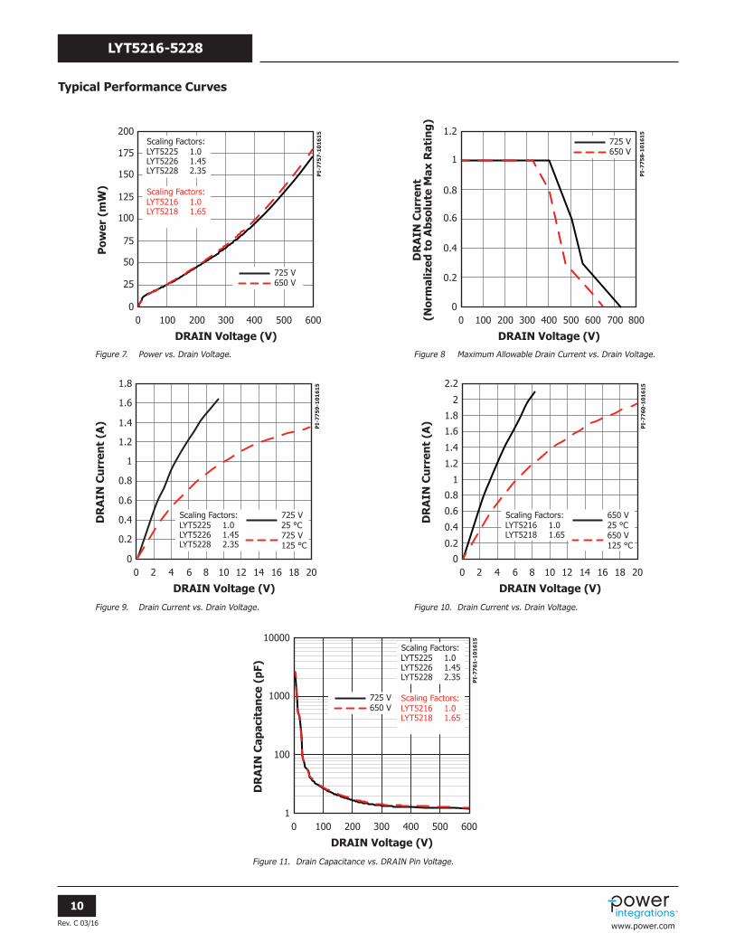
Typical Performance Curves
200
100
125
175
150
25
50
75
00 100 200 300 400 500 600
DRAIN Voltage (V)
Pow
er (
mW
)
PI-
77
57
-10
16
15
725 V650 V
LYT5225 1.0LYT5226 1.45LYT5228 2.35
Scaling Factors:
LYT5216 1.0LYT5218 1.65
Scaling Factors:
1.2
0.6
0.8
1
0.2
0.4
00 100 200 300 400 500 600 700 800
DRAIN Voltage (V)
DR
AIN
Cu
rren
t(N
orm
aliz
ed t
o A
bsol
ute
Max
Rat
ing)
PI-
77
58
-10
16
15
725 V650 V
1.8
1.6
0.8
1
1.4
1.2
0.2
0.4
0.6
00 2 4 6 8 10 12 14 16 18 20
DRAIN Voltage (V)
DR
AIN
Cu
rren
t (A
) PI-
77
59
-10
16
15
725 V25 °C725 V125 °C
LYT5225 1.0LYT5226 1.45LYT5228 2.35
Scaling Factors:
2.2
1.8
2
0.8
1.2
1
1.6
1.4
0.2
0.4
0.6
00 2 4 6 8 10 12 14 16 18 20
DRAIN Voltage (V)
DR
AIN
Cu
rren
t (A
) PI-
77
60
-10
16
15
650 V25 °C650 V125 °C
LYT5216 1.0LYT5218 1.65
Scaling Factors:
10000
100
1000
10 100 200 300 400 500 600
DRAIN Voltage (V)
DR
AIN
Cap
acit
ance
(pF
)
PI-
77
61
-10
16
15
725 V650 V
LYT5225 1.0LYT5226 1.45LYT5228 2.35
Scaling Factors:
LYT5216 1.0LYT5218 1.65
Scaling Factors:
Figure 7. Power vs. Drain Voltage.
Figure 9. Drain Current vs. Drain Voltage. Figure 10. Drain Current vs. Drain Voltage.
Figure 11. Drain Capacitance vs. DRAIN Pin Voltage.
Figure 8 Maximum Allowable Drain Current vs. Drain Voltage.

Rev. C 03/16
11
LYT5216-5228
www.power.com
PI-7473-061515POD-SO-16B Rev A
Notes:1. Dimensioning and tolerancing per ASME Y14.5M-1994.
2. Dimensions noted are determined at the outermost extremes of the plastic body exclusive of mold flash, tie bar burrs, gate burrs, and inter-lead flash, but including any mismatch between the top and bottom of the plastic body. Maximum mold protrusion is 0.25 mm per side.
3. Dimensions noted are inclusive of plating thickness.
4. Does not include inter-lead flash or protrusions.
5. Dimensions in Inches [mm].
6. Datums A and B to be determined in Datum H.
7. JEDEC reference: MS − 012.
SO-16B
Seating Plane
SeatingPlane
0.044 [1.10] Ref.
0.054 [1.38] Ref.
0.010 [0.25]
Detail A
Gauge Plane
Pin #1 I.D.(Laser Marked)
0.032 [0.81]0.022 [0.56]
0.066 [1.69]0.057 [1.46]
0.153 [3.90]
0.050 [1.27]
0.010 [0.25]0.004 [0.10]
0.010 [0.25]0.004 [0.10]
TOP VIEW
DETAIL A
SIDE VIEW
END VIEW
0.004 [0.10] 2X C B
0.004 [0.10] 2X C A
0.004 [0.10]
14 Leads
8 Lead Tips
6 Lead Tips
C
0.005 [0.13] C
0.005 [0.13]
0.239 [6.07]
0.390 [9.91]
0.135 [3.43]Ref.
C
H
CB
A
C
16 9
1 8 8º0º
14X0.019 [0.48]0.013 [0.33]
0.010 [0.25] M C A B
43
2
2
Rev. C 03/16
12
LYT5216-5228
www.power.com
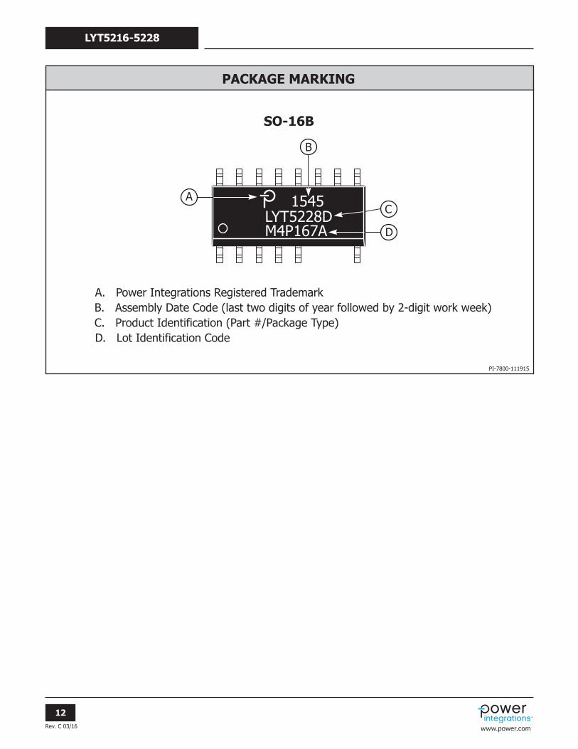
1545LYT5228DM4P167A
PI-7800-111915
SO-16B
A. Power Integrations Registered TrademarkB. Assembly Date Code (last two digits of year followed by 2-digit work week)C. Product Identification (Part #/Package Type)D. Lot Identification Code
PACKAGE MARKING
A
B
C
D

Rev. C 03/16
13
LYT5216-5228
www.power.com
MSL Table
Part Number MSL Rating
LYT5225D 3
LYT5216D 3
LYT5226D 3
LYT5218D 3
LYT5228D 3
ESD and Latch-Up Table
Test Conditions Results
Latch-up at 125 °C JESD78D > ±100 mA or > 2.5 kV (max) on all pins
Human Body Model ESD JESD22-A114F > ±2000 V on all pins
Machine Model ESD JESD22-A115A > ±200 V on all pins
Part Ordering Information
• LYTSwitch-5 Product Family
• Series Number
• MOSFET VDS Rating
1 650 V
2 725 V
• Device Size
• Package Identifier
D SO-16B
• Tape & Reel and Other Options
Blank Tube of 50 pcs.
TL Tape & Reel, 2500 pcs min/mult.LYT 52 2 5 D- TL

Revision Notes Date
B Code A Release. 11/15
B Made text corrections to LYTSwitch-5 Output Regulation section and PCB Layout Considerations section. Corrections made to Figures 5 and 6. 12/03/15
B Updated Figures 1a and 1b. Modified text in 1st paragraph of Input Filter section on page 4. 12/11/15
C Corrected IS2, TLEB, TFB, TSD, IOOV parameters. Added IOUV and VL parameters. 03/16
For the latest updates, visit our website: www.power.comPower Integrations reserves the right to make changes to its products at any time to improve reliability or manufacturability. Power Integrations does not assume any liability arising from the use of any device or circuit described herein. POWER INTEGRATIONS MAKES NO WARRANTY HEREIN AND SPECIFICALLY DISCLAIMS ALL WARRANTIES INCLUDING, WITHOUT LIMITATION, THE IMPLIED WARRANTIES OF MERCHANTABILITY, FITNESS FOR A PARTICULAR PURPOSE, AND NON-INFRINGEMENT OF THIRD PARTY RIGHTS.
Patent InformationThe products and applications illustrated herein (including transformer construction and circuits external to the products) may be covered by one or more U.S. and foreign patents, or potentially by pending U.S. and foreign patent applications assigned to Power Integrations. A complete list of Power Integrations patents may be found at www.power.com. Power Integrations grants its customers a license under certain patent rights as set forth at http://www.power.com/ip.htm.
Life Support PolicyPOWER INTEGRATIONS PRODUCTS ARE NOT AUTHORIZED FOR USE AS CRITICAL COMPONENTS IN LIFE SUPPORT DEVICES OR SYSTEMS WITHOUT THE EXPRESS WRITTEN APPROVAL OF THE PRESIDENT OF POWER INTEGRATIONS. As used herein:
1. A Life support device or system is one which, (i) is intended for surgical implant into the body, or (ii) supports or sustains life, and (iii) whose failure to perform, when properly used in accordance with instructions for use, can be reasonably expected to result in significant injury or death to the user.
2. A critical component is any component of a life support device or system whose failure to perform can be reasonably expected to cause the failure of the life support device or system, or to affect its safety or effectiveness.
The PI logo, TOPSwitch, TinySwitch, LinkSwitch, LYTSwitch, InnoSwitch, DPA-Switch, PeakSwitch, CAPZero, SENZero, LinkZero, HiperPFS, HiperTFS, HiperLCS, Qspeed, EcoSmart, Clampless, E-Shield, Filterfuse, FluxLink, StakFET, PI Expert and PI FACTS are trademarks of Power Integrations, Inc. Other trademarks are property of their respective companies. ©2016, Power Integrations, Inc.
World Headquarters5245 Hellyer AvenueSan Jose, CA 95138, USA.Main: +1-408-414-9200Customer Service:Phone: +1-408-414-9665Fax: +1-408-414-9765e-mail: [email protected]
China (Shanghai)Rm 2410, Charity Plaza, No. 88North Caoxi RoadShanghai, PRC 200030Phone: +86-21-6354-6323Fax: +86-21-6354-6325e-mail: [email protected]
China (Shenzhen)17/F, Hivac Building, No. 2, Keji Nan 8th Road, Nanshan District, Shenzhen, China, 518057Phone: +86-755-8672-8689Fax: +86-755-8672-8690e-mail: [email protected]
GermanyLindwurmstrasse 11480337 MunichGermanyPhone: +49-895-527-39110Fax: +49-895-527-39200e-mail: [email protected]
India#1, 14th Main RoadVasanthanagarBangalore-560052 IndiaPhone: +91-80-4113-8020Fax: +91-80-4113-8023e-mail: [email protected]
ItalyVia Milanese 20, 3rd. Fl.20099 Sesto San Giovanni (MI) ItalyPhone: +39-024-550-8701Fax: +39-028-928-6009e-mail: [email protected]
JapanKosei Dai-3 Bldg. 2-12-11, Shin-Yokohama, Kohoku-ku Yokohama-shi, Kanagawa 222-0033 JapanPhone: +81-45-471-1021Fax: +81-45-471-3717e-mail: [email protected]
KoreaRM 602, 6FLKorea City Air Terminal B/D, 159-6Samsung-Dong, Kangnam-Gu,Seoul, 135-728, KoreaPhone: +82-2-2016-6610Fax: +82-2-2016-6630e-mail: [email protected]
Singapore51 Newton Road#19-01/05 Goldhill PlazaSingapore, 308900Phone: +65-6358-2160Fax: +65-6358-2015e-mail: [email protected]
Taiwan5F, No. 318, Nei Hu Rd., Sec. 1Nei Hu Dist.Taipei 11493, Taiwan R.O.C.Phone: +886-2-2659-4570Fax: +886-2-2659-4550e-mail: [email protected]
UKCambridge Semiconductor,a Power Integrations companyWestbrook Centre, Block 5, 2nd FloorMilton RoadCambridge CB4 1YGPhone: +44 (0) 1223-446483e-mail: [email protected]
Power Integrations Worldwide Sales Support Locations