Embed Size (px)
Citation preview

POE PD POWER SUPPLY EVALUATION BOARD USER GUIDE
Microsemi Analog Mixed Signal Group
11861 Western Avenue, Garden Grove, CA. 92841, 714-898-8121, Fax: 714-893-2570 Page 1Copyright © 2008
Rev. 1.0, 2008-12-18
TTrriippllee IIssoollaatteedd PPoowweerr SSuuppppllyy ffoorr PPOOEE PPoowweerreedd DDeevviiccee
AApppplliiccaattiioonn UUssiinngg UUCC33884444 aanndd LLXX11775522
Evaluation Board

POE PD POWER SUPPLY EVALUATION BOARD USER GUIDE
Microsemi Analog Mixed Signal Group
11861 Western Avenue, Garden Grove, CA. 92841, 714-898-8121, Fax: 714-893-2570 Page 2Copyright © 2008
Rev. 1.0, 2008-12-18
CONTENTS
INTRODUCTION………………………………………………………………………………………..3 KEY FEATURES………………………………………………………………………………………..3 APPLICATIONS………………………………………………………………………………………...3 ORDERING INFORMATION……………………………………………………………………………..3 OPERATION……………………………………………………………………………………………4 PERFORMANCE………………………………………………………...………………………………5-7 EVALUATION BOARD SCHEMATIC…………………………………………………………………….8-10 BILL OF MATERIALS…………………………………………………………………………………..11-13 PCB LAYOUT………………………………………………………………………………………….14-18 TEST SETUP & PROCEDURE…….……………………………………………………………………...19-20

POE PD POWER SUPPLY EVALUATION BOARD USER GUIDE
Microsemi Analog Mixed Signal Group
11861 Western Avenue, Garden Grove, CA. 92841, 714-898-8121, Fax: 714-893-2570 Page 3Copyright © 2008
Rev. 1.0, 2008-12-18
Introduction to Product The multi-output power supply evaluation board is a fully assembled and tested printed circuit board (PCB) that provides three step-down regulated output voltages with a 36V to 57V input at 13W. The power supply is designed for Power Over Ethernet (POE) applications, specifically the Powered Device (PD) or the receiver end. Figure 1 shows a block diagram of the PD power supply. The power supply consists of the following sections: Input filter and rectifier, PD interface, EMI filter, 5V output isolated flyback converter, and 5V to 3.3V and 1.8V non-isolated step down converters. The UC3844 is designed as the isolated flyback converter and the LX1752 generates the step down dual outputs. The flyback converter is configured using 13W. The power capability of the design can be increased to 30W by changing the flyback transformer and output rectifier diode to a higher power rating. Note that the power supply circuitry (minus the PD interface) is not limited to POE applications and can be used in any application requiring a 36V to 57V input and step down output(s) adjusted for the required voltage(s). Figure 1 – Block Diagram
36V to 57V POE Input
Input Filter and
Rectifier
PD Interface
EMIFilter
IsolatedFlyback
5V to 3.3VStep-Down
5V to 1.8V Step-Down
5VDC
3.3VDC
1.8VDC
Key Features: 36V to 57V Input Range Output Voltages 5V (Isolated Flyback Output) 3.3V (Step-down Switching Regulator) 1.8V (Step-down Switching Regulator) 13Watt Input Adjustable Output Voltages using External Resistors 70% Overall Efficiency Power Device Interface Applications: Power Over Ethernet Powered Device / Receiver End Supply Multi-output Power Supply Ordering Information: Part # LX1752-POE-PD13W

POE PD POWER SUPPLY EVALUATION BOARD USER GUIDE
Microsemi Analog Mixed Signal Group
11861 Western Avenue, Garden Grove, CA. 92841, 714-898-8121, Fax: 714-893-2570 Page 4Copyright © 2008
Rev. 1.0, 2008-12-18
Evaluation Board Operation: The evaluation board accepts a 36V to 57V input via a CAT-5 cable connected to the Ethernet connector port (J1). The connector J1 integrates an RF transformer for Ethernet data coupling and also an input filter that conducts RF interferences to chassis ground. Connector J2 routes and outputs the Ethernet data from port J1. The diode bridges (U1 and U2), which allow the positive and negative terminals of the input supply to be interchanged, are rated at 1.5A. The Powered Device (PD) interface consists of a detection, classification, and isolation circuits. The detection block supports two different detection schemes, which comprises of a 25kΩ resistor detection, as required by the IEEE 802.3a standard, and also an input capacitor detection. Classification is optionally performed by the Power Sourcing Equipment (PSE) to determine the level of power consumption by the PD. Isolation circuitry blocks power from the PSE to the flyback during detection and classification. For a detailed explanation of the Power Device interface, refer to Application Note AN-125. The isolated flyback converter uses the UC3844 current mode controller set to operate at 200kHz. The converter runs in a discontinuous mode. The isolated feedback is provided using an opto-isolator driven by an error amplifier made from a TL431. Additional compensation is provided using the error amplifier contained within the UC3844. The power transformer T1 has a primary side inductance of 27uH +/-15%. Note that upon initial power up, the flyback controller (U3) is kick-started by the energy stored in C13, which is charged up by the input voltage source. After startup, the auxiliary winding will generate the bootstrap voltage to keep U3 enabled. The power transformer also includes a reset winding via an ultra-fast rectifier diode (D8) to ground, to clamp leakage inductance overshoots when M2 turns off and also to provide a path that returns the leakage energy to the input for improving efficiency. To further prevent premature startup of the flyback converter, the circuitry consisting of Q6, Q7, and Q8 is a comparator used to hold off the UC3844 by providing a low impedance path from the COMP output through Q8 to ground until M1 is completely turned on. When M1 is turned off, the base voltage of Q6 will be less than the base voltage of Q7, driving the gate of Q8 high. When M1 is turned on and the input voltage rises to its nominal value, the base voltage of Q6 will be higher than the base voltage of Q7, pulling the gate of Q8 low to turn it off, allowing the COMP pin to rise to start the flyback circuit. A soft-start is implemented by adding D11, C18, and R30 to the COMP pin of the UC3844 since the COMP pin voltage directly controls the maximum current through the switch. Finally, note that since the flyback converter has a pulsed input current, an EMI filter is included to prevent the 200kHz current chop from becoming conducted emissions. The EMI filter consists of L4, C6, and C7. The final stage of the POE PD power supply consists of the LX1752 buck regulator configured to operate at a switching frequency of 800kHz, with output voltages set at 1.8V and 3.3V. The buck inputs, the input supply VIN to the LX1752, and VCCL of the LX1752 are powered by the 5V output of the flyback and are all tied to the same node. Feedback compensation of the LX1752 is provided externally using type 2. The current limit for both outputs is set at approximately 5A and can be externally adjusted. For more information regarding the LX1752, please refer to the device datasheet.

POE PD POWER SUPPLY EVALUATION BOARD USER GUIDE
Microsemi Analog Mixed Signal Group
11861 Western Avenue, Garden Grove, CA. 92841, 714-898-8121, Fax: 714-893-2570 Page 5Copyright © 2008
Rev. 1.0, 2008-12-18
Performance: Performance of the POE PD Power Supply is observed for 13W at the input under the following conditions:
Nominal Output Voltage
Output Current
1.8V 1A 3.3V 1A 5V 0.75A
Overall Efficiency at Full Load Conditions The overall efficiency is the total output power of the 3 regulated outputs with respect to the input power applied at the Ethernet port connector.
VIN=36V 70.5%
VIN=48V 70%
Overall Efficiency (includes the diode bridges, PD interface, filters, Flyback, and Buck) 5V @ 0.75A 1.8V @ 1A 3.3V @ 1A VIN=57V 69.7%
LX1752 Buck Efficiency 1.8V @ 1A 3.3V @ 1A
VIN=5V 92.6%
Output Ripple Output Voltage No Load Full Load 5V Flyback Output, VIN = 48V 10mVpp 16mVpp
1.8V Step-Down Output, VIN = 48V 15mVpp 17mVpp
3.3V Step-Down Output, VIN=48V 20mVpp 22mVpp
Line Regulation 5V @0.75A, VIN=36V, 57V <0.1%
1.8V @1A, VIN=36V, 57V <0.1%
3.3V @1A, VIN=36V, 57V <0.1%
Load Regulation 5V @ no load and 0.75A, VIN=48V <0.1%
1.8V @ no load and 1A, VIN=48V <0.1%
3.3V @ no load and 1A, VIN=48V <0.1%

POE PD POWER SUPPLY EVALUATION BOARD USER GUIDE
Microsemi Analog Mixed Signal Group
11861 Western Avenue, Garden Grove, CA. 92841, 714-898-8121, Fax: 714-893-2570 Page 6Copyright © 2008
Rev. 1.0, 2008-12-18
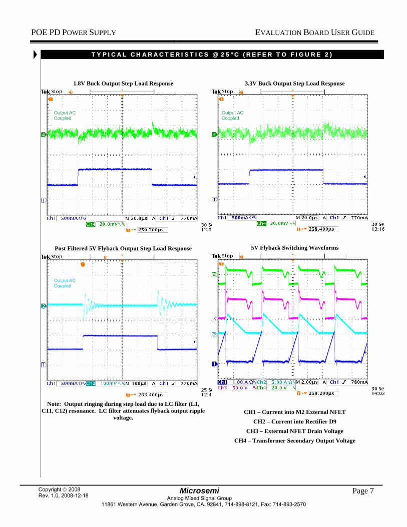
T Y P I C A L C H A R A C TE R I S T I C S @ 2 5 ° C ( R E F E R T O F I G U R E 2 )
Hot Insertion Startup Under Full Load Conditions
CH1 – POE Input Source CH4 – POE Input Current
CH2 – Flyback Input Voltage CH3 – 5V Flyback Output Loaded at 750mA
Hot Insertion Startup Under Full Load Conditions
CH1 – POE Input Source CH2 – 5V Flyback Output at 750mA
CH3 – 3.3V Buck Output at 1A CH4 – 1.8V Buck Output at 1A
PowerDsine 3001 limits inrush currents
POE PD POWER SUPPLY EVALUATION BOARD USER GUIDE
Microsemi Analog Mixed Signal Group
11861 Western Avenue, Garden Grove, CA. 92841, 714-898-8121, Fax: 714-893-2570 Page 7Copyright © 2008
Rev. 1.0, 2008-12-18
T Y P I C A L C H A R A C TE R I S T I C S @ 2 5 ° C ( R E F E R T O F I G U R E 2 )
1.8V Buck Output Step Load Response
Post Filtered 5V Flyback Output Step Load Response
Note: Output ringing during step load due to LC filter (L1, C11, C12) resonance. LC filter attenuates flyback output ripple
voltage.
3.3V Buck Output Step Load Response
5V Flyback Switching Waveforms
CH1 – Current into M2 External NFET
CH2 – Current into Rectifier D9 CH3 – Extermal NFET Drain Voltage
CH4 – Transformer Secondary Output Voltage
Output AC Coupled
Output AC Coupled
Output AC Coupled

POE PD POWER SUPPLY EVALUATION BOARD USER GUIDE
Microsemi Analog Mixed Signal Group
11861 Western Avenue, Garden Grove, CA. 92841, 714-898-8121, Fax: 714-893-2570 Page 8Copyright © 2008
Rev. 1.0, 2008-12-18
Schematic
SHLDSHLD
+1.8V
TD+RD+
VC1+NUNU
CTVC2+
VC1-TD-RD-
TX+
NUVC2-
RX+TX-
RX-NUNU
SHLDNUNU
SHLD
J2
557484-1
12345678S1S2
D6
BZX84C10
R920k
J3
CON12
123456789
101112
Q4MMBTA06
D4BZX84C24
RAWGND
GND
R1349.9k
R14475kD7
BZX84C5V1
R324.9k
C10.1uF100V
C247nF100V
Q1KST92
D3BZX84C11
GND
R551.1k
GNDGND
Q3KST92
R11475k
GNDGND
5V@3A MAX5V@3A MAX
3.3V@4A MAX
R12475k
C3100pF
3.3V@4A MAX
1.8V@5A MAX
48V
1.8V@5A MAX
R10422k
Q2MMBTA06
Detection Block
R1475k
48VRTN
R4475k
R210k
R6511
R7511
R8511
D1BZX84C12
C40.1uf
Isolation Block
- +
U1
DF005M
1
3
2
4
Classification Block is stuffed on the evaluation board and optionally performed by the PSE.
- +
U2
DF005M
1
3
2
4D5
1SMA58A
Q52N7002
D2BZX84C30
J1
0813-1X1T-57F
123456789101112S1S2
+5V
M1
STD16NF06
+3.3V
Note: For different levels of classification, R2 must be adjusted to the proper value. See AN-125 for details.
Figure 2 – Ethernet Connectors, Diode Bridges, PD Interface Schematic

POE PD POWER SUPPLY EVALUATION BOARD USER GUIDE
Microsemi Analog Mixed Signal Group
11861 Western Avenue, Garden Grove, CA. 92841, 714-898-8121, Fax: 714-893-2570 Page 9Copyright © 2008
Rev. 1.0, 2008-12-18
Schematic
C70.1uF100V
R1911.5k
+C10
820uF/6.3V
L1
1uH
1 2
C1110uF6.3V
C1210uF6.3V
R17118k
C14
1000p2500V
R181M
R22221k
R381.0k
R161.0M
R351.0k
R283.01k
C171000pF
R21
255k
C150.01uF
+5VA
D10
CDBA-140
T1
HA3905-CL Coilcraf t
3
1
25
6
97
10
4
8
R2075
M2
FQD10N20
C8330pF
L4
100uH1 2
R290.43
Q6
2N3906
+5V
R27
1.0kC16100pF
R26
2.7
R301M
C184.7uF R31
750
D9
MBRS320
CMR1U-02MD8
+C13
47uF/35V
U4TL431AIDR
RAWGND
D11
PMBD914
R32
1k
Q7
2N3906
C22
NU
C20NU
C19
1uF
R15
NU
C5
NU
R33
118kC21
NU
48V
48VRTN
R24
1M
Q82N7002
R36
10k
R2516.2k
ISO1SFH6156-2
21
43
R371.0k
R231M
R34NU
+ C6
180uF/63V
U3
UC3844
COMP1
VFB2
ISNS3
RT/CT4
GND5
OUT6
VCC7
VREF8
+C9
820uF/6.3V
Figure 3 – 48V to 5V Isolated Flyback Schematic

POE PD POWER SUPPLY EVALUATION BOARD USER GUIDE
Microsemi Analog Mixed Signal Group
11861 Western Avenue, Garden Grove, CA. 92841, 714-898-8121, Fax: 714-893-2570 Page 10Copyright © 2008
Rev. 1.0, 2008-12-18
Schematic
+5VA
+5VA
R522.00K
C28
10uF
C32 0.22uF
R461K
R441K
+5VA
+5VA
C411.0uF
+5VA
C24 0.1uF
3
54
7
1
6
2
2
8
8 7
5
3
1
4
6
R47
2.00K
Q9AFDS6911
Q9BFDS6911
+ C27
NU
+C30
820uF6.3V
L2 3.3uH
R49 NU
+5VA
R48 160K
R50
5.62K
C3110uF6.3V
C34 NU
C35 1.2nF
C37 NU
R51 21.0KC404.7uF
6.3V
U5
LX1752
GND1
SYNC2
SHDN23
SSEN24
EA2-5
EO26
VIN7
CS28
VS2
9
VC
210
HO
211
HR
212
VC
CL
13
LO2
14
VRE
F28
PS
ET27
RF
REQ
26
SSEN
125
EA1-
24
EO1
23
SHDN122
CS1 21
VS1 20
VC119
HO118
HR1 17
LO1 16
PGND15
C25
1.0uF
+5VA
C381.0uF
C43
10uF
C33 0.1uF
C361uF
C39
1.0uF
R40
NU
R45
160K
R41
13.3k
C26 NU
C29
1.2nF
C44 0.1uF
+1.8V
C23
NUR42
21.0K
Q10BFDS6911
Q10AFDS6911
CR1
CMDSH-3
+ C42
NU
+C46820uF6.3V
L3 3.3uH
VIA
C45
10uF6.3V
R431K
CR2
CMDSH-3
R39
40.2K
+3.3V
Figure 3 – 5V to 1.8V and 3.3V Dual Output Step-Down Converter Schematic

POE PD POWER SUPPLY EVALUATION BOARD USER GUIDE
Microsemi Analog Mixed Signal Group
11861 Western Avenue, Garden Grove, CA. 92841, 714-898-8121, Fax: 714-893-2570 Page 11Copyright © 2008
Rev. 1.0, 2008-12-18
Evaluation Board Build Of Materials
13W POE PD Evaluation Board BOM Qty Reference Designators Part Number Value Vendor Package Type
2 C1, 7 GCM21BR72A104 0.1uF, 100V Murata 805
1 C2 GRM21BR72A473 47nF, 100V Murata 805
2 C3,16 ECJ-1VC1H101K 100pF, 50V Panasonic 603
4 C4, 24, 33, 44 ECJ-1VB1E104K 0.1uF, 25V Panasonic 603
1 C6 UHE1J181MPD 180uF, 63V Nichicon 10x20
1 C8 ECJ-2VB2D331K 330pF, 200V Panasonic 805
4 C9, 10, 30, 46 6.3MCZ820M8X11.5 820uF, 6.3V Rubycon 8.0 x 11.5
6 C11, 12, 28, 31, 43, 45 JMK212BJ106M 10uF, 6.3V Taiyo Yuden 805
1 C13 ECA-1VHG470 47uF, 35V Panasonic 5.0 x 11
1 C14 62O102MQECS 1000pF, 2500V AVX Through hole
1 C15 ECJ-1VB1C103 0.01uF, 16V Panasonic 603
1 C17 ECJ-1VB1H102 1000pF, 50V Panasonic 603
2 C18, 40 JMK212BJ475M 4.7uF, 6.3V Taiyo Yuden 805
8 C19, 25, 36, 38, 39, 41, 43, 45
JMK212BJ105M 1uF, 16V Taiyo Yuden 805
3 C5, 27, 42 Not Used Through hole
7 C20, 21, 22, 23, 26, 34, 37 Not Used 603
2 C29, 35 ECJ-1VB1H122 1200pF, 50V Panasonic 603
1 C32 ECJ-1VB1E224K 0.22uF, 25V Panasonic 603
2 CR1, 2 CMDSH-3 30V, 100mA Central Semi SOD-323
1 D1 BZX84C12 Zener, 12V, 5% Philips SOT-23
1 D2 BZX84C30 Zener, 30V, 5% Philips SOT-23
1 D3 BZX84C11 Zener, 11V, 5% Philips SOT-23
1 D4 BZX84C24 Zener, 24V, 5% Philips SOT-23
1 D5 1SMA58A 58V, 400W, TVS On Semi SMA
1 D6 BZX84C10 Zener, 10V, 5% Philips SOT-23

POE PD POWER SUPPLY EVALUATION BOARD USER GUIDE
Microsemi Analog Mixed Signal Group
11861 Western Avenue, Garden Grove, CA. 92841, 714-898-8121, Fax: 714-893-2570 Page 12Copyright © 2008
Rev. 1.0, 2008-12-18
1 D7 BZX84C5V1 Zener, 5.1V, 5% Philips SOT-23
1 D8 CMR1U-02M 200V, 1A Central Semi SMA
1 D9 MBRS320 20V, 3A On Semi SMC
1 D10 CDBA140-G 40V, 1A Comchip SMA
1 D11 PMBD914 75V, 215mA Philips SOT-23
1 ISO1 SFH6156-2 Opto, CTR 100% Vishay SMD-4
1 J1 0813-1X1T-57F RJ-45 POE Bel Non std
1 J2 557484-1 RJ-45 Tyco Non std
1 J3 p/o PBC36SFCN 12 p x 0.1”ctr Sullins 16 pin header
1 L1 2643000801 1uH Fair-rite Ferrite bead
2 L2, 3 SPC-10049P-3R3 3.3uH 6A TMP 10x10
1 L4 SMI-0805-0101 100uH, 1.2A TMP 13.3 x 9.4
1 M1 STD16NF06L Nch, 60V, 24A ST Micro DPAK
1 M2 FQD10N20 Nch, 200V, 7.8A Fairchild DPAK
2 Q1, 3 KST92 PNP,300V, 0.5A Fairchild SOT-23
2 Q2, 4 MMBTA06 NPN,80V, 300mA
On Semi SC-70
2 Q6, Q7 SMBT3906 Dual PNP, 40V Infineon SOT-363
2 Q5, 8 2N7002 Nch, 60V, 385mA
Philips SOT-23
2 Q9, 10 FDS6911 Dual Nch 20V 7.5A
Fairchild SOIC8
5 R1, 4, 11, 12, 14 ERJ-6ENF4753V 475k, 1/8W Panasonic 805
1 R2 ERJ-6ENF1002V 10.0k, 1/8W Panasonic 805
1 R3 ERJ-6ENF2492V 24.9k, 1/8W Panasonic 805
1 R5 ERJ-3EKF2492V 51.1, 1/10W Panasonic 603
3 R6, 7, 8 ERJ-6ENF5110V 511, 1/8W Panasonic 805
1 R9 ERJ-6ENF2002V 20k, 1/8W Panasonic 805
1 R10 ERJ-6EKF4223V 422k, 1/10W Panasonic 603
1 R13 ERJ-3EKF4992V 49.9k, 1/10W Panasonic 603
5 R16, 18, 23, 24, 30 ERJ-3EKF105V 1.0M, 1/10W Panasonic 603

POE PD POWER SUPPLY EVALUATION BOARD USER GUIDE
Microsemi Analog Mixed Signal Group
11861 Western Avenue, Garden Grove, CA. 92841, 714-898-8121, Fax: 714-893-2570 Page 13Copyright © 2008
Rev. 1.0, 2008-12-18
2 R17, R33 ERJ-3EKF1183V 118k, 1/10W Panasonic 603
1 R25 ERJ-6ENF1622V 16.2k, 1/8W Panasonic 805
1 R19 ERJ-6ENF1152V 11.5k, 1/8W Panasonic 805
1 R20 RMC1/875R01%G 75 1/4W SEI 1206
1 R21 ERJ-3EKF2553V 255k, 1/10W Panasonic 603
1 R22 ERJ-3EKF2213V 221k, 1/10W Panasonic 603
1 R26 ERJ-3GEYJ2R7V 2.7, 1/10W Panasonic 603
8 R27, 32, 35, 37, 38, 43, 44, 46
ERJ-3EKF1001V 1.00k, 1/10W Panasonic 603
1 R28 ERJ-3EKF3011V 3.01k, 1/10W Panasonic 603
1 R29 73L6R47J 0.47, 3/4W CTS 2010
1 R31 ERJ-3EKF7500V 750, 1/10W Panasonic 603
1 R36 ERJ-3EKF1002V 10k, 1/10W Panasonic 603
1 R39 ERJ-3EKF4022V 40.2k, 1/10W Panasonic 603
3 R34, 40, 49 Not Used 603
1 R15 Not Used 1206
1 R41 ERJ-3EKF1332V 13.3k, 1/10W Panasonic 603
2 R42, 51 ERJ-3EKF2102V 21.0k, 1/10W Panasonic 603
2 R45, 48 ERJ-3EKF1603V 160k, 1/10W Panasonic 603
2 R47, 52 ERJ-3EKF2001V 2.0k, 1/10W Panasonic 603
1 R50 ERJ-3EKF5621V 5.62k, 1/10W Panasonic 603
1 T1 HA3905-CL Flyback Tfmr Coilcraft
2 U1,2 DF005S Bridge Rect Fairchild SDIP
1 U3 UC3844ADM CMPS Controller Microsemi SOIC8
1 U4 TL431AIDR Shunt Regulator TI SOIC8
1 U5 LX1752CLQ Dual PWM Microsemi MLPQ28

POE PD POWER SUPPLY EVALUATION BOARD USER GUIDE
Microsemi Analog Mixed Signal Group
11861 Western Avenue, Garden Grove, CA. 92841, 714-898-8121, Fax: 714-893-2570 Page 14Copyright © 2008
Rev. 1.0, 2008-12-18
Evaluation Board PCB Layout Top Silkscreen and Solder Mask Top Layer

POE PD POWER SUPPLY EVALUATION BOARD USER GUIDE
Microsemi Analog Mixed Signal Group
11861 Western Avenue, Garden Grove, CA. 92841, 714-898-8121, Fax: 714-893-2570 Page 15Copyright © 2008
Rev. 1.0, 2008-12-18
Top Layer

POE PD POWER SUPPLY EVALUATION BOARD USER GUIDE
Microsemi Analog Mixed Signal Group
11861 Western Avenue, Garden Grove, CA. 92841, 714-898-8121, Fax: 714-893-2570 Page 16Copyright © 2008
Rev. 1.0, 2008-12-18
Inner Layer 2

POE PD POWER SUPPLY EVALUATION BOARD USER GUIDE
Microsemi Analog Mixed Signal Group
11861 Western Avenue, Garden Grove, CA. 92841, 714-898-8121, Fax: 714-893-2570 Page 17Copyright © 2008
Rev. 1.0, 2008-12-18
Inner Layer 3 Bottom Layer

POE PD POWER SUPPLY EVALUATION BOARD USER GUIDE
Microsemi Analog Mixed Signal Group
11861 Western Avenue, Garden Grove, CA. 92841, 714-898-8121, Fax: 714-893-2570 Page 18Copyright © 2008
Rev. 1.0, 2008-12-18
Bottom Layer

POE PD POWER SUPPLY EVALUATION BOARD USER GUIDE
Microsemi Analog Mixed Signal Group
11861 Western Avenue, Garden Grove, CA. 92841, 714-898-8121, Fax: 714-893-2570 Page 19Copyright © 2008
Rev. 1.0, 2008-12-18
Test Setup:
Test Procedure: The following is a demonstration scenario that can be used to evaluate the POE PD power supply:
1) The evaluation board can be powered over Ethernet via 48V, or by a regular external power supply for testing without network connectivity.
2) To verify the circuit operation over the full input range, use a bench top DC power supply capable of generating a voltage range of 36V to 57V and a current output of 1A for sourcing power via either node VC1+/VC1- or VC2+/VC2-. Set the power supply current limit to 500mA. Insure that the supply is shut off before connecting.
3) For power over Ethernet interface, use a POE source such as the PowerDsine 3001 Midspan from Microsemi and connect the Data & Power Out Port to the evaluation board port J1 via a CAT-5 cable. The evaluation board should now be powered by 48V.
4) If using an external power supply, set the supply voltage to 57V. Turn on the power supply. Without any output load currents, verify that the input current from the supply is below 30mA.
5) Using an oscilloscope, monitor the 5V output of the flyback at connector J3. Also monitor the step-down outputs of 1.8V and 3.3V at connector J3.
6) Using DMM (Digital Multi Meter), verify the nominal output DC voltages are stable at connector J3: +5VDC nominal +/-3%, +1.8VDC nominal +/-3%, +3.3VDC nominal +/-3%
7) Test load regulation. Using resistive load or electronic load, apply a 1A load at each of the 1.8V and 3.3V output, and a 750mA load at the 5V output. Monitor with DVM that the output voltages remain within 3% of the nominal. Note that the input current from the external power supply will be approximately 228mA at 57V or 270mA at 48V.
8) Test line regulation at full load conditions: Reduce the power supply voltage from 57V to 36V and verify that the output voltages remain within +/-3% of the nominal output voltages. Line regulation test is only applicable using external power supply to adjust the input voltage.
9) With power over Ethernet, connect another CAT-5 cable from port J2 to a computer for network connectivity. Actual setup using PowerDsine 3001 Midspan is shown below and can be used to verify actual network connectivity.

POE PD POWER SUPPLY EVALUATION BOARD USER GUIDE
Microsemi Analog Mixed Signal Group
11861 Western Avenue, Garden Grove, CA. 92841, 714-898-8121, Fax: 714-893-2570 Page 20Copyright © 2008
Rev. 1.0, 2008-12-18
Power Over Ethernet Using PowerDsine 3001 Midspan for Network Connectivity
PowerDsine 3001 Midspan
POE PD Evaluation Board
CAT-5 Ethernet Connection (grey cable), Data In, No Power
PowerDsine 3001 provides Data Out & Power Out via CAT-5 (blue cable) to port J1 of POE PD Evaluation Board
Port J2 Provides Data Interface to Computer