Embed Size (px)
Citation preview

Intel’s Broadwell
03.05.2016 2

Qualcomm’s Snapdragon 810
03.05.2016 3

AMD Bristol Ridge
4Departement Informationstechnologie und Elektrotechnik
Heterogeneous Multicores
Deszo Sima (Univ. Budapest)

Vocabulary in the multi-era
AMP (Asymmetric MP) Each processor has local memory Tasks statically allocated to one processor
SMP (Symmetric MP) Processors share memory Tasks dynamically scheduled to any processor

Vocabulary in the multi-era
Heterogeneous: Specialization among processors Often different instruction sets Usually AMP design
Homogeneous: All processors have the same instruction set Processors can run any task Usually SMP design

Future many-coresLocally homogeneous
Globally heterogeneous

ARM big.LITTLE
• DVFS• Task Migration• SW Overhead• Memory coherency

ARM big.LITTLE Energy Saving

Exclusive useof the clusters
Inclusive useof the clusters
Exclusive/inclusive use of the clusters
Clusters are used exclusively,i.e. at a time one of the clusters is in use
as shown below for the cluster migration model(to be discussed later)
Clusters are used inclusively,i.e. at a time both clusters can be used
partly or entirely
Cache coherent interconnect
Cluster of big cores
CPU0 CPU1
CPU2 CPU3
CPU0 CPU1
CPU2 CPU3
Cache coherent interconnect
Cluster ofLITTLE cores
CPU0 CPU1
CPU2 CPU3
Cluster ofbig cores
CPU0 CPU1
CPU2 CPU3
Cluster of LITTLE cores
Cache coherent interconnect
Cluster of big cores
CPU0 CPU1
CPU2 CPU3
CPU0 CPU1
CPU2 CPU3
Cache coherent interconnect
Cluster ofLITTLE cores
CPU0 CPU1
CPU2 CPU3
Cluster ofbig cores
Cluster of LITTLE cores
CPU0 CPU1
CPU2 CPU3
Exclusive/inclusive use of the clusters
Low load High load Low load High load
4.3 Principle of ARM’s big.LITTLE technology (3)

Usage models of synchronous adaptive SMPs in the n + n configuration
Usage models of synchronous adaptive SMPs in the n+n configuration
Exclusive/inclusiveuse of the clusters
The cluster migration model
4.3 Principle of ARM’s big.LITTLE technology (2)

Exclusive useof the clusters
Inclusive useof the clusters
Cluster migration Core migration Core migration
big.LITTLE MPbig.LITTLE processingwith cluster migration
big.LITTLE processingwith core migration
The cluster migration model
The cluster migration model [5]
4.3 Principle of ARM’s big.LITTLE technology (4)

• There are two core clusters, the LITTLE core cluster andthe big core cluster.
• Tasks run on either the LITTLE or the big core cluster, soonly one core cluster is active at any time (except a shortinterval during a cluster switch).
• Low workloads, such as background synch tasks, audio orvideo playback run typically on the LITTLE core cluster.
• If the workload becomes higher than the max performance of the LITTLE core cluster the workload will be migratedto the big core cluster and vice versa.
Big.LITTLE processing with cluster migration [5]
4.3 Principle of ARM’s big.LITTLE technology (5)
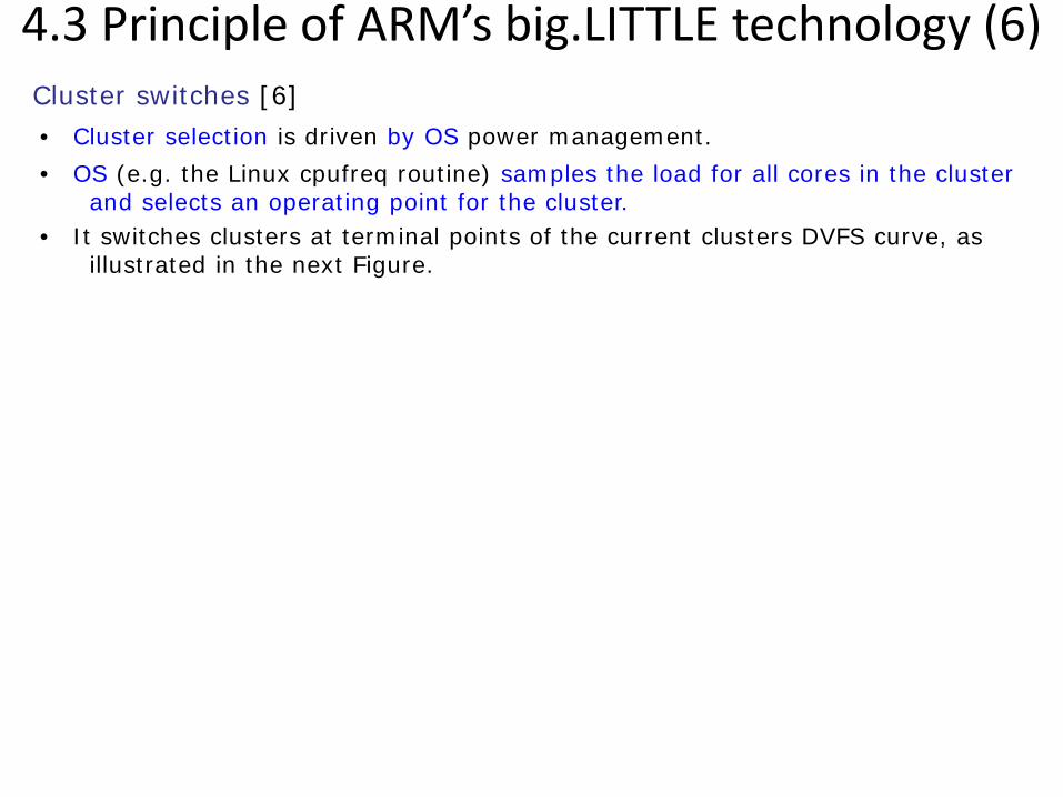
• Cluster selection is driven by OS power management.• OS (e.g. the Linux cpufreq routine) samples the load for all cores in the cluster
and selects an operating point for the cluster.• It switches clusters at terminal points of the current clusters DVFS curve, as
illustrated in the next Figure.
Cluster switches [6]
4.3 Principle of ARM’s big.LITTLE technology (6)

Power/performance curve during cluster switching [7]
(Low power core)
(High performance core)
DVFS operating points
• A switch from the low power cluster to the high performance cluster is an extension of the DVFS strategy.
• A cluster switch lasts about 30 kcycles.
4.3 Principle of ARM’s big.LITTLE technology (7)

Big.LITTLE processing with core migration [5], [8]
• There are two core clusters, the LITTLE core cluster andthe big core cluster.
• Cores are grouped into pairs of one big core and oneLITTLE core.
The LITTLE and the big core of a group are used exclusively.• Each LITTLE core can switch to its big counterpart if it meets a
higher load than its max. performance and vice versa.• Each core switch is independent from the others.
4.3 Principle of ARM’s big.LITTLE technology (8)

Core switches [6]
• Core selection in any core pair is performed by OS power management.• The DVFS algorithm monitors the core load.
When a LITTLE core cannot service the actual load, a switch to its big counterpartis initiated and the LITTLE core is turned off and vice versa.
4.3 Principle of ARM’s big.LITTLE technology (9)

big.LITTLE MP processing with core migration [8],[5]
• The OS scheduler has all cores of both clusters at its disposal and can activate all cores at any time.
• Tasks can run or be moved between the LITTLE cores andthe big cores as decided by the scheduler.
• big.LITTLE MP termed also as Heterogeneous Multiprocessing(HMP).
4.3 Principle of ARM’s big.LITTLE technology (10)

Exclusive useof the clusters
Inclusive useof the clusters
Cluster migration Core migration Core migration
big.LITTLE MP(Heterogeneous Multiprocessing)
big.LITTLE processingwith cluster migration
big.LITTLE processingwith core migration
big.LITTLE tecnology
Use of the big.LITTLE technology in recent mobile processors
Samsung Exynos 5Octa 5410 (2013)
(4 + 4 cores)
Samsung HMP on Exynos 5
Octa 5420 (2013)(4 + 4 cores)
Used in
Described first in ARM’s White Paper (2012) [9]
Mediatek MT 8135 (2013)(2 + 2 cores)
Renesas MP 6530 (2013)(2 + 2 cores)
Described first in ARM’s White Paper (2011) [3]
Described first in ARM’s White Paper (2011) [3]
4.3 Principle of ARM’s big.LITTLE technology (11)

CPU+GPU integration
Deszo Sima (Univ. Budapest)

1. Introduction to architectural integration of the CPU and GPU (1)
1. Introduction to architectural integration of the CPU and GPU
Heterogeneous processing
Aim of architectural integration of the CPU and GPU
Accelerated graphics processing
• Accelerating HPC by the GPU,i.e. by the large number of FP units available in a GPU.
• Accelerating graphics processingby the higher bandwidth of connecting the CPU and the GPU.
• Cost reductionNeeds HLL support (CUDA, OPenCL)

Unified system memory(Shared memory)
(Unified Virtual Memory)(Unified Memory Architecture)
Implementation of the graphics memory
Discrete graphics memory
Implementation alternatives of graphics memory [1]
Implementation example
Typ. use Graphics cards On-die integrated graphics
1. Introduction to architectural integration of the CPU and GPU (2)

It eliminates the need for an extra graphics memory controller and bus but has the constraints of a reduced memory bandwidth.
Key benefit/drawback of the Unified system memory [1]
Unified system memory(Shared memory)
(Unified Virtual Memory)(Unified Memory Architecture)
Implementation of the graphics memory
Discrete graphics memory
Implementation example
1. Introduction to architectural integration of the CPU and GPU (3)

Address spaces for Discrete and Unified System Memory (USM) [2]
USMNo USM
1. Introduction to architectural integration of the CPU and GPU (4)

Main difficulty of heterogeneous computing
• GPUs operate from their own address spaces, thus without appropriate hardware and software
support data to be processed by GPUs need to be loaded into their address space and
the results need to be sent back to the host. • Transferring data may be avoided with unified system memory and suitable
software support(CUDA 4.0 or OpenCL 1.2 or higher) assuming appropriate hardware.
Then data transfer will be substituted by address mapping (called zero copy).
1. Introduction to architectural integration of the CPU and GPU (5)

Tasks to be performed for copying data/mapping address spaces for GPUs [1]
1. Introduction to architectural integration of the CPU and GPU (6)

2. AMD’s approach to support heterogeneous computing

Aim of HSA-1 [4]
2.1 Introduction to HSA (2)

Aim of HSA-2 [5]
2.1 Introduction to HSA (3)

The entire HSA solution stack [6]
HSAIL: HSA Intermediate Language
2.1 Introduction to HSA (4)

Establishment of the HAS Foundation
• In 6/2012 AMD, ARM, TI Qualcomm, Samsung and several otherleading semiconductor firms established the Heterogeneous System Architecture (HSA) Foundation.
• It is a non-profit consortium that aims at defining and promoting open standards for heterogeneous computing.
2.1 Introduction to HSA (5)

2.2 Key hardware enhancements neededto implement HSA

2.2 Key hardware enhancements needed to implement HSA [5]
2.2 Key hardware enhancements needed to implement HSA (1)
hUMA: heterogeneous UMA UMA: Uniform Memory Access

2.2.1 hUMA (Heterogeneous Uniform Memory Access)
2.2 Key hardware enhancements needed to implement HSA (2)
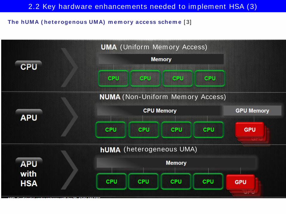
(Non-Uniform Memory Access)
(Uniform Memory Access)
(heterogeneous UMA)
The hUMA (heterogenous UMA) memory access scheme [3]
2.2 Key hardware enhancements needed to implement HSA (3)

GPU co-processing of data structures without hUMA [3]
2.2 Key hardware enhancements needed to implement HSA (4)

GPU co-processing of data structures with hUMA [3]
2.2 Key hardware enhancements needed to implement HSA (5)
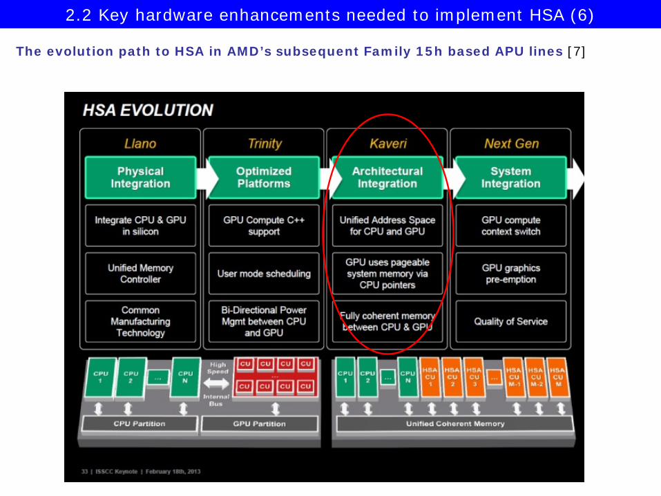
The evolution path to HSA in AMD’s subsequent Family 15h based APU lines [7]
2.2 Key hardware enhancements needed to implement HSA (6)

Key requirements of hUMA-1 [3]
2.2 Key hardware enhancements needed to implement HSA (7)
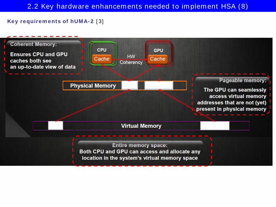
Key requirements of hUMA-2 [3]
2.2 Key hardware enhancements needed to implement HSA (8)

AMD Tech Day 2014 Jan
Hardware support of memory management in Kaveri [8]
2.2 Key hardware enhancements needed to implement HSA (9)
2.2.2 hQ (heterogeneous Queuing)
2.2 Key hardware enhancements needed to implement HSA (10)
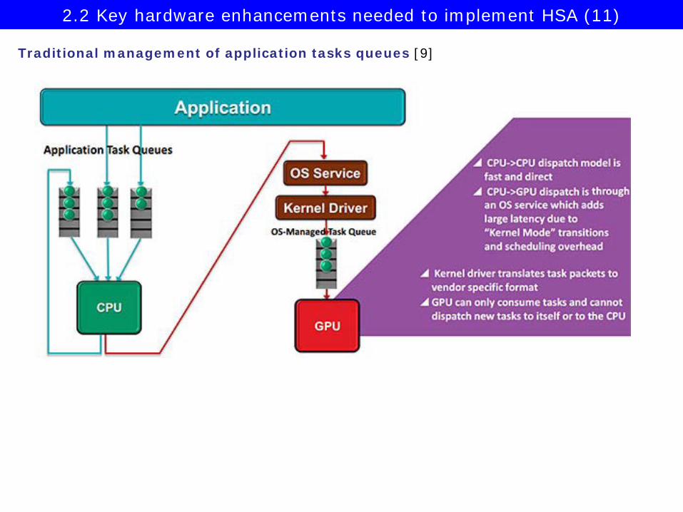
Traditional management of application tasks queues [9]
2.2 Key hardware enhancements needed to implement HSA (11)

Application task management with heterogeneous queuing (hQ) [9]
2.2 Key hardware enhancements needed to implement HSA (12)

• Heterogeneous queuing (hQ) is symmetrical.It allows both the CPU and the GPU to generate tasks for themselves and for each other.
• Work is specified in a standard packet format that will be supported by all HSA-compatible hardware, sothere's no need for the software to use vendor-specific code.
• Applications can put packets directly into the task queues that will be accessed by the hardware.• Each application can have multiple task queues, and a virtualization layer allows HSA hardware to see all
the queues.
Main features of hQ [9]
2.2 Key hardware enhancements needed to implement HSA (13)

3. Intel’s approach to support heterogeneous computing

3.1 Intel’s implementations of integrated graphics (1)
3.1 Intel’s implementations of integrated graphics
Intel has a long history of integrated graphics, implemented first in the north bridge in the8xx chipset (1999), as indicated below.
Implementation of integrated graphics
In the north bridge On the processor dieIn a multi-chip processor package on a separate die
Both the CPU and the GPU are on separate diesand are mounted into a single package
Implementations about1999 – 2009 such as
Intel’s 828xx chipset (1999)and subsequent implementations
P
South Bridge
Mem.NBIG
South Bridge
Mem.NB
PGPU CPU
Periph. Contr.
Mem.CPUGPUP
Intel’s Havendale (DT) andAuburndale (M)
(scheduled for 1H/2009but cancelled)
Arrandale (DT, 1/2010) andClarkdale (M, 1/2010)
Intel’s Sandy Bridge (1/2011) andsubsequent processors
AMD’s Swift (scheduled for 2009but canceled)
AMD’s Bobcat-based APUs (M, 1/2011)Llano APUs (DT, 6/2011)
and subsequent processors

Unified Memory Architecture (UMA)
Some early graphics cards of other vendors and essentially all (in the north bridge) integrated graphics designs of Intel already made use of the UMA design as early as in the second halfof the 1990s, as the next Figure shows for the integrated graphics of the Intel 810 chipset (1999)
Figure: The UMA design of an early (in the north bridge) integrated graphics [12]
The UMA design eliminates the need for an extra graphics memory controller and bus but has theconstraints of a reduced memory bandwidth.
Key benefit/drawback of the UMA design
CPUGraphics/Memory
Controller
Gfx/MemoryArbiter
OptionalDisplayCache
System memory FB
DirectAGP
3.1 Intel’s implementations of integrated graphics (2)

Intel’s on-die integrated graphics designs
Subsequently, we discuss only those on-die integrated CPU-GPU solutions that support also HPCi.e. have OpenCL support, as follows.
Table: Intel’s processors with on-die integrated GPUs [13]
3.1 Intel’s implementations of integrated graphics (3)
OpenCL2.0
OpenCL1.2
OpenCL1.2
OpenCL1.2
NoOpenCL
OpenCLsupport

Key benefit of OpenCL 1.2 supported Shared Physical Memory, illustrated on an example[13]
3.1 Intel’s implementations of integrated graphics (4)

Shared Virtual Memory - based on the Broadwell architecture and supported by OpenCL 2.0 [13]
3.1 Intel’s implementations of integrated graphics (5)

Key OpenCL 2.0 features [14]
3.1 Intel’s implementations of integrated graphics (6)

3.2 Intel’s first implementation of Shared Virtual Memory The Core M processor

3.2 Intel’s first implementation of Shared Virtual Memory – The Core M (1)
3.2 Intel’s first implementation of Shared Virtual Memory – The Core M processor
• The Core M processor targets tablets and 2-in-1 devices• Based on the 14 nm Broadwell architecture• Includes Gen8 graphics• It is a SOC (System on Chip) design• Announced: 8/2014.

Die layout of the Core M [13]
3.2 Intel’s first implementation of Shared Virtual Memory – The Core M (3)

Block diagram of the Core M [13]
3.2 Intel’s first implementation of Shared Virtual Memory – The Core M (4)

Compute architecture of Core M [13]
3.2 Intel’s first implementation of Shared Virtual Memory – The Core M (7)