Embed Size (px)
Citation preview

LTM8065
1Rev.B
For more information www.analog.com
TYPICAL APPLICATION
FEATURES
APPLICATIONS
DESCRIPTION
40VIN, 2.5A Silent Switcher µModule Regulator
The LTM®8065 is a 40VIN, 3.5A peak, 2.5A continuous step-down µModule® (power module) regulator. Included in the package are the switching controller, power switches, inductor and all support components. Operating over an input voltage range of 3.4V to 40V, the LTM8065 supports an output voltage range of 0.97V to 18V and a switching frequency range of 200kHz to 3MHz, each set by a single resistor. Only the input and output filter capacitors are needed to finish the design.
The low profile package enables utilization of unused space on the bottom of PC boards for high density point of load regulation. The LTM8065 is packaged in a thermally enhanced, compact over-molded ball grid array (BGA) pack-age suitable for automated assembly by standard surface mount equipment. The LTM8065 is RoHS compliant.All registered trademarks and trademarks are the property of their respective owners.
Efficiency vs Load Current
5VOUT from 7VIN to 40VIN Step-Down Converter
n Complete Step-Down Switch Mode Power Supply n Low Noise Silent Switcher® Architecture n Wide Input Voltage Range: 3.4V to 40V n Wide Output Voltage Range: 0.97V to 18V n 2.5A Continuous Output Current, 3.5A Peak n Selectable Switching Frequency: 200kHz to 3MHz n External Synchronization n Programmable Soft-Start n Tiny, Low Profile 6.25mm × 6.25mm × 2.32mm
RoHS Compliant BGA Package
n Automotive Battery Regulation n Power for Portable Products n Distributed Supply Regulation n Industrial Supplies n Wall Transformer Regulation
2.2µF
22µF60.4k41.2k
1MHz
LTM8065
VOUTVOUT5V2.5A3.5A PEAK
VINVIN7V TO 40V
FBGND
RUN
SYNC
RT
8065 TA01a
PINS NOT USED IN THIS CIRCUIT: TR/SS, PG
AUXBIAS
LOAD CURRENT (A)
VIN = 12V
0 1 2 380
85
90
95
EFFI
CIEN
CY (%
)
8065 TA01b
Document Feedback

LTM8065
2Rev.B
For more information www.analog.com
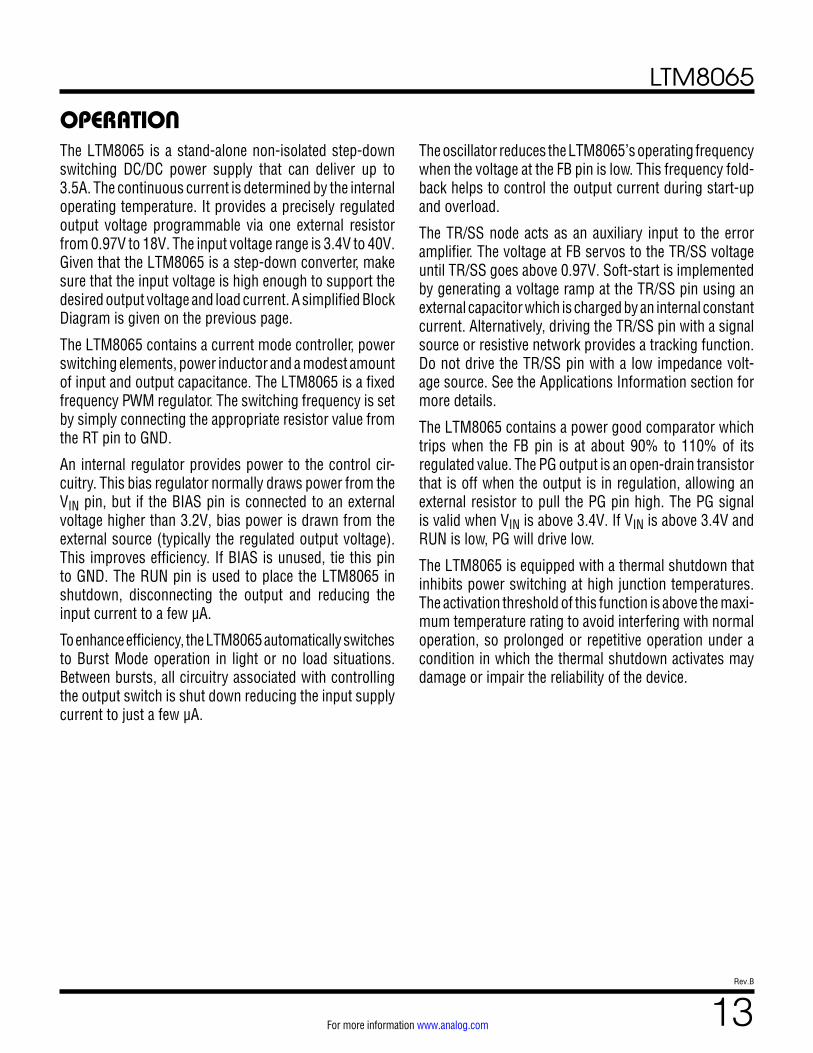
PIN CONFIGURATIONABSOLUTE MAXIMUM RATINGS
VIN, RUN, PG Voltage .............................................. 42VAUX, VOUT, BIAS Voltage ........................................ 19VFB, TR/SS Voltage ..................................................... 4VSYNC Voltage ............................................................ 6VMaximum Internal Temperature .......................... 125°CStorage Temperature ............................ –55°C to 125°CPeak Reflow Solder Body Temperature ............... 260°C
(Notes 1, 2)
GND
BANK 1 GND
BANK 3 VOUT
BANK 2VIN
F
E
A
B
C
D
21 43 5 6
BGA PACKAGE36-LEAD (6.25mm × 6.25mm × 2.32mm) BGA PACKAGE
BIAS
FB
PG
SYNCAUX TR/SS
RT
TOP VIEW
GND GND
RUN
TJMAX = 125°C, θJA = 21°C/W, θJCbottom = 5.9°C/W θJCtop = 36.5°C/W, θJB = 6.3°C/W, WEIGHT = 0.5gθ VALUES DETERMINED PER JEDEC51-9, 51-12
ORDER INFORMATION
PART NUMBER TERMINAL FINISH
PART MARKING* PACKAGE TYPE
MSL RATING TEMPERATURE RANGEDEVICE FINISH CODE
LTM8065EY#PBFSAC305 (RoHS) LTM8065 e1 BGA 3 –40°C to 125°C
LTM8065IY#PBF
• Contact the factory for parts specified with wider operating temperature ranges. *Pad or ball finish code is per IPC/JEDEC J-STD-609.
• Recommended LGA and BGA PCB Assembly and Manufacturing Procedures
• LGA and BGA Package and Tray Drawings

LTM8065
3Rev.B
For more information www.analog.com
ELECTRICAL CHARACTERISTICS
Note 1: Stresses beyond those listed under Absolute Maximum Ratings may cause permanent damage to the device. Exposure to any Absolute Maximum Rating condition for extended periods may affect device reliability and lifetime.Note 2: Unless otherwise noted, the absolute minimum voltage is zero.Note 3: The LTM8065E is guaranteed to meet performance specifications from 0°C to 125°C internal. Specifications over the full –40°C to 125°C internal operating temperature range are assured by design, characterization and correlation with statistical process controls. The LTM8065I is guaranteed to meet specifications over the full –40°C to 125°C internal operating temperature range. Note that the maximum internal temperature is determined by specific operating conditions in conjunction with board layout, the rated package thermal resistance and other environmental factors.
PARAMETER CONDITIONS MIN TYP MAX UNITS
Minimum Input Voltage VIN Rising l 3.4 V
Output DC Voltage RFB Open RFB = 14.3kΩ, VIN = 40V
0.97 18
V V
Peak Output DC Current VOUT = 3.3V, fSW = 1MHz 3.5 A
Quiescent Current into VIN RUN = 0V BIAS = 0V, No Load, SYNC = 0V, Not Switching
3 8
µA µA
Quiescent Current into BIAS BIAS = 5V, RUN = 0V BIAS = 5V, No Load, SYNC = 0V, Not Switching BIAS = 5V, VOUT = 3.3V, IOUT = 2.5A, fSW = 1MHz
1 5
12
µA µA
mA
Line Regulation 5.5V < VIN < 36V, IOUT = 1A 0.5 %
Load Regulation 0.1A < IOUT < 2.5A 0.5 %
Output Voltage Ripple IOUT = 2.5A 10 mV
Switching Frequency RT = 232kΩ RT = 41.2kΩ RT = 10.7kΩ
200 1 3
kHz MHz MHz
Voltage at FB l 950 970 980 mV
Minimum BIAS Voltage (Note 5) 3.2 V
RUN Threshold Voltage 0.9 1.06 V
RUN Current 1 µA
TR/SS Current TR/SS = 0V 2 µA
TR/SS Pull Down TR/SS = 0.1V 200 Ω
PG Threshold Voltage at FB (Upper) FB Falling (Note 6) 1.05 V
PG Threshold Voltage at FB (Lower) FB Rising (Note 6) 0.89 V
PG Leakage Current PG = 42V 1 µA
PG Sink Current PG = 0.1V 150 µA
SYNC Threshold Voltage Synchronization 0.4 1.5 V
SYNC Voltage To Enable Spread Spectrum 2.9 4.2 V
SYNC Current SYNC = 0V 35 µA
The l denotes the specifications which apply over the specified operating temperature range, otherwise specifications are at TJ = 25°C. VIN = 12V, RUN = 2V, unless otherwise noted.
Note 4: The LTM8065 contains overtemperature protection that is intended to protect the device during momentary overload conditions. The internal temperature exceeds the maximum operating junction temperature when the overtemperature protection is active. Continuous operation above the specified maximum operating junction temperature may impair device reliability.Note 5: Below this specified voltage, internal circuitry will draw power from VIN.Note 6: PG transitions from low to high.

LTM8065
4Rev.B
For more information www.analog.com
TYPICAL PERFORMANCE CHARACTERISTICS
Efficiency, VOUT = 0.97V, BIAS = 5V
Efficiency, VOUT = 1.2V, BIAS = 5V
Efficiency, VOUT = 1.5V, BIAS = 5V
TA = 25°C, unless otherwise noted.
Efficiency, VOUT = 1.8V, BIAS = 5V
Efficiency, VOUT = 2V, BIAS = 5V
Efficiency, VOUT = 2.5V, BIAS = 5V
Efficiency, VOUT = 3.3V, BIAS = 5V
Efficiency, VOUT = 5V, BIAS = 5V
Efficiency, VOUT = 8V, BIAS = 5V
12VIN24VIN36VIN
LOAD CURRENT (A)0 1 2 3
45
55
65
75
85
EFFI
CIEN
CY (%
)
8065 G01
12VIN24VIN36VIN
LOAD CURRENT (A)0 1 2 3
45
55
65
75
85
EFFI
CIEN
CY (%
)
8065 G02
12VIN24VIN36VIN
LOAD CURRENT (A)0 1 2 3
50
60
70
80
90
EFFI
CIEN
CY (%
)
8065 G03
12VIN24VIN36VIN
LOAD CURRENT (A)0 1 2 3
50
60
70
80
90
EFFI
CIEN
CY (%
)
8065 G04
12VIN24VIN36VIN
LOAD CURRENT (A)0 1 2 3
50
60
70
80
90
EFFI
CIEN
CY (%
)
8065 G05
12VIN24VIN36VIN
LOAD CURRENT (A)0 1 2 3
50
60
70
80
90
EFFI
CIEN
CY (%
)
8065 G06
12VIN24VIN36VIN
LOAD CURRENT (A)0 1 2 3
55
65
75
85
95
EFFI
CIEN
CY (%
)
8065 G07
12VIN24VIN36VIN
LOAD CURRENT (A)0 1 2 3
55
65
75
85
95
EFFI
CIEN
CY (%
)
8065 G08
12VIN24VIN36VIN
LOAD CURRENT (A)0 1 2 3
60
70
80
90
100
EFFI
CIEN
CY (%
)
8065 G09

LTM8065
5Rev.B
For more information www.analog.com
TYPICAL PERFORMANCE CHARACTERISTICS TA = 25°C, unless otherwise noted.
Efficiency, VOUT = 12V, BIAS = 5V
Efficiency, VOUT = 15V, BIAS = 5V
Efficiency, VOUT = 18V, BIAS = 5V
Efficiency, VOUT = –3.3V, BIAS tied to LTM8065 GND
Efficiency, VOUT = –5V, BIAS tied to LTM8065 GND
Efficiency, VOUT = –8V, BIAS tied to LTM8065 GND
Efficiency, VOUT = –12V, BIAS tied to LTM8065 GND
Efficiency, VOUT = –15V, BIAS tied to LTM8065 GND
Efficiency, VOUT = –18V, BIAS tied to LTM8065 GND
24VIN36VIN
LOAD CURRENT (A)0 1 2 3
60
70
80
90
100
EFFI
CIEN
CY (%
)
8065 G10
24VIN36VIN
LOAD CURRENT (A)0 1 2 3
60
70
80
90
100
EFFI
CIEN
CY (%
)
8002 G11
24VIN36VIN
LOAD CURRENT (A)0 1 2 3
60
70
80
90
100
EFFI
CIEN
CY (%
)
8065 G12
12VIN24VIN35VIN
LOAD CURRENT (A)0 1 2 3
60
65
70
75
80
85
EFFI
CIEN
CY (%
)
8065 G13
12VIN24VIN
LOAD CURRENT (A)0 1 2 3
50
60
70
80
90
EFFI
CIEN
CY (%
)
8065 G14
12VIN24VIN
LOAD CURRENT (A)0 1 2 3
50
60
70
80
90
EFFI
CIEN
CY (%
)
8065 G15
12VIN24VIN
LOAD CURRENT (A)0 0.5 1 1.5 2
60
65
70
75
80
85
EFFI
CIEN
CY (%
)
8065 G16
12VIN24VIN
LOAD CURRENT (A)0 0.5 1 1.5
50
60
70
80
90
EFFI
CIEN
CY (%
)
8065 G17
12VIN
LOAD CURRENT (A)0 0.25 0.50 0.75 1 1.25
60
65
70
75
80
85
EFFI
CIEN
CY (%
)
8065 G18

LTM8065
6Rev.B
For more information www.analog.com
TYPICAL PERFORMANCE CHARACTERISTICS
Input vs Load Current VOUT = 0.97V
Input vs Load Current VOUT = 1.2V
Input vs Load Current VOUT = 1.5V
Input vs Load Current VOUT = 1.8V
Input vs Load Current VOUT = 2V
Input vs Load Current VOUT = 2.5V
Input vs Load Current VOUT = 3.3V
Input vs Load Current VOUT = 5V
Input vs Load Current VOUT = 8V
TA = 25°C, unless otherwise noted.
12VIN24VIN36VIN
LOAD CURRENT (A)0 0.5 1 1.5 2 2.5 3 3.5
0
0.2
0.4
0.6
INPU
T CU
RREN
T (A
)
8065 G19
12VIN24VIN36VIN
LOAD CURRENT (A)0 0.5 1 1.5 2 2.5 3 3.5
0
0.2
0.4
0.6
INPU
T CU
RREN
T (A
)
8065 G20
12VIN24VIN36VIN
LOAD CURRENT (A)0 0.5 1 1.5 2 2.5 3 3.5
0
0.2
0.4
0.6
INPU
T CU
RREN
T (A
)
8065 G21
12VIN24VIN36VIN
LOAD CURRENT (A)0 0.5 1 1.5 2 2.5 3 3.5
0
0.2
0.4
0.6
0.8
INPU
T CU
RREN
T (A
)
8065 G22
12VIN24VIN36VIN
LOAD CURRENT (A)0 0.5 1 1.5 2 2.5 3 3.5
0
0.3
0.6
0.9
INPU
T CU
RREN
T (A
)
8065 G23
12VIN24VIN36VIN
LOAD CURRENT (A)0 0.5 1 1.5 2 2.5 3 3.5
0
0.4
0.8
1.2
INPU
T CU
RREN
T (A
)
8065 G24
12VIN24VIN36VIN
LOAD CURRENT (A)0 0.5 1 1.5 2 2.5 3 3.5
0
0.5
1.0
1.5
INPU
T CU
RREN
T (A
)
8065 G25
12VIN24VIN36VIN
LOAD CURRENT (A)0 0.5 1 1.5 2 2.5 3 3.5
0
0.5
1.0
1.5
2.0
INPU
T CU
RREN
T (A
)
8065 G26
12VIN24VIN36VIN
LOAD CURRENT (A)0 0.5 1 1.5 2 2.5 3 3.5
0
1
2
3
INPU
T CU
RREN
T (A
)
8065 G27

LTM8065
7Rev.B
For more information www.analog.com
TYPICAL PERFORMANCE CHARACTERISTICS TA = 25°C, unless otherwise noted.
Input vs Load Current VOUT = 12V
Input vs Load Current VOUT = 15V
Input vs Load Current VOUT = 18V
Input vs Load Current VOUT = –3.3V
Input vs Load Current VOUT = –5V
Input vs Load Current VOUT = –8V
Input vs Load Current VOUT = –12V
Input vs Load Current VOUT = –15V
Input vs Load Current VOUT = –18V
24VIN36VIN
LOAD CURRENT (A)0 0.5 1 1.5 2 2.5 3 3.5
0
0.5
1.0
1.5
2.0
INPU
T CU
RREN
T (A
)
8065 G28
24VIN36VIN
LOAD CURRENT (A)0 0.5 1 1.5 2 2.5 3 3.5
0
1
2
3
INPU
T CU
RREN
T (A
)
8065 G29
12VIN24VIN36VIN
LOAD CURRENT (A)0 1 2 3 4
0
0.5
1.0
1.5
INPU
T CU
RREN
T (A
)
8065 G31
12VIN24VIN
LOAD CURRENT (A)0 1 2 3 4
0
0.5
1.0
1.5
2.0
INPU
T CU
RREN
T (A
)
8065 G32
12VIN24VIN
LOAD CURRENT (A)0 1 2 3
0
0.5
1.0
1.5
2.0
INPU
T CU
RREN
T (A
)
8065 G33
12VIN24VIN
LOAD CURRENT (A)0 0.5 1 1.5 2
0
0.5
1.0
1.5
2.0
2.5
INPU
T CU
RREN
T (A
)
8065 G34
24VIN36VIN
LOAD CURRENT (A)0 0.5 1 1.5 2 2.5 3 3.5
0
1
2
3
INPU
T CU
RREN
T (A
)
8065 G30
12VIN24VIN
LOAD CURRENT (A)0 0.5 1 1.5
0
0.5
1.0
1.5
2.0
2.5
INPU
T CU
RREN
T (A
)
8065 G35
12VIN
LOAD CURRENT (A)0 0.5 1 1.5
0
0.5
1.0
1.5
2.0
2.5
INPU
T CU
RREN
T (A
)
8065 G36

LTM8065
8Rev.B
For more information www.analog.com
Maximum Load Current vs VIN BIAS tied to LTM8065 GND
Derating, VOUT = 0.97V BIAS = 5V, DC2251A Demo Board
Maximum Load Current vs VIN BIAS tied to LTM8065 GND
TYPICAL PERFORMANCE CHARACTERISTICS
Derating, VOUT = 1.2V, BIAS = 5V, DC2251A Demo Board
Derating, VOUT = 1.5V, BIAS = 5V, DC2251A Demo Board
Derating, VOUT = 1.8V, BIAS = 5V, DC2251A Demo Board
Derating, VOUT = 2V, BIAS = 5V, DC2251A Demo Board
TA = 25°C, unless otherwise noted.
Derating, VOUT = 2.5V, BIAS = 5V, DC2251A Demo Board
Derating, VOUT = 3.3V, BIAS = 5V, DC2251A Demo Board
–3.3VOUT–5VOUT–8VOUT
INPUT VOLTAGE (V)0 10 20 30 40
0
1
2
3
4
5
MAX
IMUM
LOA
D CU
RREN
T (A
)
8065 G37
–12VOUT–15VOUT–18VOUT
INPUT VOLTAGE (V)0 10 20 30
0
0.5
1.0
1.5
2.0
MAX
IMUM
LOA
D CU
RREN
T (A
)
8065 G38
0 LFM
12VIN24VIN36VIN
AMBIENT TEMPERATURE (°C)0 25 50 75 100 125
0
1
2
3
4
MAX
IMUM
LOA
D CU
RREN
T (A
)
8065 G39
0 LFM
12VIN24VIN36VIN
AMBIENT TEMPERATURE (°C)0 25 50 75 100 125
0
1
2
3
4
MAX
IMUM
LOA
D CU
RREN
T (A
)
8065 G40
0 LFM
12VIN24VIN36VIN
AMBIENT TEMPERATURE (°C)0 25 50 75 100 125
0
1
2
3
4
MAX
IMUM
LOA
D CU
RREN
T (A
)
8065 G41
0 LFM
12VIN24VIN36VIN
AMBIENT TEMPERATURE (°C)0 25 50 75 100 125
0
1
2
3
4
MAX
IMUM
LOA
D CU
RREN
T (A
)
8065 G42
0 LFM
12VIN24VIN36VIN
AMBIENT TEMPERATURE (°C)0 25 50 75 100 125
0
1
2
3
4
MAX
IMUM
LOA
D CU
RREN
T (A
)
8065 G43
0 LFM
12VIN24VIN36VIN
AMBIENT TEMPERATURE (°C)0 25 50 75 100 125
0
1
2
3
4
MAX
IMUM
LOA
D CU
RREN
T (A
)
8065 G44
0 LFM
12VIN24VIN36VIN
AMBIENT TEMPERATURE (°C)0 25 50 75 100 125
0
1
2
3
4
MAX
IMUM
LOA
D CU
RREN
T (A
)
8065 G45

LTM8065
9Rev.B
For more information www.analog.com
TYPICAL PERFORMANCE CHARACTERISTICS TA = 25°C, unless otherwise noted.
Derating, VOUT = 3.3V, BIAS = 5V, DC2251A Demo Board
Derating, VOUT = 5V, BIAS = 5V, DC2251A Demo Board
Derating, VOUT = 5V, BIAS = 5V, DC2251A Demo Board
Derating, VOUT = 8V, BIAS = 5V, DC2251A Demo Board
Derating, VOUT = 12V, BIAS = 5V, DC2251A Demo Board
Derating, VOUT = 15V, BIAS = 5V, DC2251A Demo Board
Derating, VOUT = 18V, BIAS = 5V, DC2251A Demo Board
Derating, VOUT = –5V, BIAS tied to LTM8065 GND, DC2251A Demo Board
Derating, VOUT = –3.3V, BIAS tied to LTM8065 GND, DC2251A Demo Board
0 LFM
24VIN36VIN
AMBIENT TEMPERATURE (°C)0 25 50 75 100 125
0
1
2
3
MAX
IMUM
LOA
D CU
RREN
T (A
)
8065 G51
0 LFM
12VIN24VIN
AMBIENT TEMPERATURE (°C)0 25 50 75 100 125
0
1
2
3
MAX
IMUM
LOA
D CU
RREN
T (A
)
8065 G54
0 LFMf = 2MHz
12VIN24VIN36VIN
AMBIENT TEMPERATURE (°C)0 25 50 75 100 125
0
1
2
3
4
MAX
IMUM
LOA
D CU
RREN
T (A
)
8065 G46
0 LFM
12VIN24VIN36VIN
AMBIENT TEMPERATURE (°C)0 25 50 75 100 125
0
1
2
3
4
MAX
IMUM
LOA
D CU
RREN
T (A
)
8065 G47
0 LFMfSW = 2MHz
12VIN24VIN36VIN
AMBIENT TEMPERATURE (°C)0 25 50 75 100 125
0
1
2
3
4
MAX
IMUM
LOA
D CU
RREN
T (A
)
8065 G48
0 LFM
12VIN24VIN36VIN
AMBIENT TEMPERATURE (°C)0 25 50 75 100 125
0
1
2
3
4
MAX
IMUM
LOA
D CU
RREN
T (A
)
8065 G49
0 LFM
24VIN36VIN
AMBIENT TEMPERATURE (°C)0 25 50 75 100 125
0
1
2
3
MAX
IMUM
LOA
D CU
RREN
T (A
)
8065 G50
0 LFM
24VIN36VIN
AMBIENT TEMPERATURE (°C)0 25 50 75 100 125
0
1
2
3
MAX
IMUM
LOA
D CU
RREN
T (A
)
8065 G52
0 LFM
12VIN24VIN36VIN
AMBIENT TEMPERATURE (°C)0 25 50 75 100 125
0
1
2
3
MAX
IMUM
LOA
D CU
RREN
T (A
)
8065 G53

LTM8065
10Rev.B
For more information www.analog.com
TYPICAL PERFORMANCE CHARACTERISTICS
Derating, VOUT = –8V, BIAS tied to LTM8065 GND, DC2251A Demo Board
Derating, VOUT = –12V, BIAS tied to LTM8065 GND, DC2251A Demo Board
Derating, VOUT = –15V, BIAS tied to LTM8065 GND, DC2251A Demo Board
Derating, VOUT = –18V, BIAS tied to LTM8065 GND, DC2251A Demo Board
CISPR22 Class B Radiated DC2251A Demo Board, VOUT = 5V No Filter (FB1, L1 short, C6, C7 open)
Dropout Voltage vs Load Current, VOUT = 5V, BIAS = 5V
TA = 25°C, unless otherwise noted.
0 LFM
12VIN24VIN
AMBIENT TEMPERATURE (°C)0 25 50 75 100 125
0
0.5
1.0
1.5
2.0
MAX
IMUM
LOA
D CU
RREN
T (A
)
8065 G55
0 LFM
12VIN24VIN
AMBIENT TEMPERATURE (°C)0 25 50 75 100 125
0
0.25
0.50
0.75
1.00
MAX
IMUM
LOA
D CU
RREN
T (A
)
8065 G56
0 LFM
12VIN24VIN
AMBIENT TEMPERATURE (°C)0 25 50 75 100 125
0
0.25
0.50
0.75
1.00
MAX
IMUM
LOA
D CU
RREN
T (A
)
8065 G57
LOAD CURRENT (A)0 1 2 3 4
0
200
400
600
800
DROP
OUT
VOLT
AGE
(mV)
8065 G59
fSW = 1MHz, VIN = 14V, IOUT = 2.5A
CLASS B LIMITHORIZONTALVERTICAL
FREQUENCY (MHz)0 200 400 600 800 1000
–10
0
10
20
30
40
50
AMPL
ITUD
E (d
BµV/
m)
8065 G60
0 LFM
12VIN
AMBIENT TEMPERATURE (°C)0 25 50 75 100 125
0
0.25
0.50
0.75
1.00
MAX
IMUM
LOA
D CU
RREN
T (A
)
8065 G58

LTM8065
11Rev.B
For more information www.analog.com
PIN FUNCTIONSGND (Bank 1, A1, A4, A6): Tie these GND pins to a local ground plane below the LTM8065 and the circuit compo-nents. In most applications, the bulk of the heat flow out of the LTM8065 is through these pads, so the printed circuit design has a large impact on the thermal performance of the part. See the PCB Layout and Thermal Considerations sections for more details.
VIN (Bank 2): VIN supplies current to the LTM8065’s in-ternal regulator and to the internal power switches. These pins must be locally bypassed with an external, low ESR capacitor; see Table 1 for recommended values.
VOUT (Bank 3): Power Output Pins. Apply the output filter capacitor and the output load between these pins and GND pins.
BIAS (Pin A2): The BIAS pin connects to the internal power bus. Connect to a power source greater than 3.2V. If VOUT is greater than 3.2V, connect this pin to AUX. If the output voltage is less, connect this to a voltage source greater than 3.2V. Decouple this pin with at least 1µF if the voltage source for BIAS is remote. If unused, tie this pin to GND.
PG (Pin A3): The PG pin is the open-collector output of an internal comparator. PG remains low until the FB pin voltage is within about 10% of the final regulation volt-age. The PG signal is valid when VIN is above 3.4V. If VIN is above 3.4V and RUN is low, PG will drive low. If this function is not used, leave this pin floating.
RT (Pin A5): The RT pin is used to program the switching frequency of the LTM8065 by connecting a resistor from this pin to ground. The Applications Information section of the data sheet includes a table to determine the resistance value based on the desired switching frequency. Minimize capacitance at this pin. Do not drive this pin.
FB (Pin B1): The LTM8065 regulates its FB pin to 0.97V. Connect the adjust resistor from this pin to ground. The value of RFB is given by the equation RFB = 241.53/(VOUT – 0.97), where RFB is in kΩ.
AUX (Pin B2): Low Current Voltage Source for BIAS. In many designs, the BIAS pin is simply connected to VOUT. The AUX pin is internally connected to VOUT and is placed adjacent to the BIAS pin to ease printed circuit board routing. Also, some applications require a feedforward capacitor; it can be connected from AUX to FB for convenient PCB routing. Although this pin is internally connected to VOUT, it is not intended to deliver a high current, so do not draw current from this pin to the load.
SYNC (Pin B4): External clock synchronization input and operational mode. This pin programs four different operating modes:
1. Burst Mode® Operation. Tie this pin to ground for Burst Mode operation at low output loads—this will result in ultralow quiescent current.
2. Pulse-skipping mode. Float this pin for pulse-skipping mode. This mode offers full frequency operation down to low output loads before pulse skipping occurs.
3. Spread spectrum mode. Tie this pin high (between 2.9V and 4.2V) for pulse-skipping mode with spread spectrum modulation.
4. Synchronization mode. Drive this pin with a clock source to synchronize to an external frequency. During synchro-nization the part will operate in pulse-skipping mode.
TR/SS (Pin B5): The TR/SS pin is used to provide a soft-start or tracking function. The internal 2μA pull-up current in combination with an external capacitor tied to this pin creates a voltage ramp. If TR/SS is less than 0.97V, the FB voltage tracks to this value. The soft-start ramp time is approximated by the equation t = 0.485 • C where C is in μF. For tracking, tie a resistor divider to this pin from the tracked output. This pin is pulled to ground with an internal MOSFET during shutdown and fault conditions; use a series resistor if driving from a low impedance output. This pin may be left floating if the tracking function is not needed.
RUN (Pin B6): Pull the RUN pin below 0.9V to shut down the LTM8065. Tie to 1.06V or more for normal operation. If the shutdown feature is not used, tie this pin to the VIN pin.

LTM8065
12Rev.B
For more information www.analog.com
BLOCK DIAGRAMLTM8065 Block Diagram
AUX
BIAS
VOUT
VIN
FB
GND
RUN
TR/SS SYNC RT PG
8065 BD01
CURRENTMODE
CONTROLLER0.2µF
10pF0.1µF
1.5µH
249k
LTM8065
13Rev.B
For more information www.analog.com
OPERATIONThe LTM8065 is a stand-alone non-isolated step-down switching DC/DC power supply that can deliver up to 3.5A. The continuous current is determined by the internal operating temperature. It provides a precisely regulated output voltage programmable via one external resistor from 0.97V to 18V. The input voltage range is 3.4V to 40V. Given that the LTM8065 is a step-down converter, make sure that the input voltage is high enough to support the desired output voltage and load current. A simplified Block Diagram is given on the previous page.
The LTM8065 contains a current mode controller, power switching elements, power inductor and a modest amount of input and output capacitance. The LTM8065 is a fixed frequency PWM regulator. The switching frequency is set by simply connecting the appropriate resistor value from the RT pin to GND.
An internal regulator provides power to the control cir-cuitry. This bias regulator normally draws power from the VIN pin, but if the BIAS pin is connected to an external voltage higher than 3.2V, bias power is drawn from the external source (typically the regulated output voltage). This improves efficiency. If BIAS is unused, tie this pin to GND. The RUN pin is used to place the LTM8065 in shutdown, disconnecting the output and reducing the input current to a few µA.
To enhance efficiency, the LTM8065 automatically switches to Burst Mode operation in light or no load situations. Between bursts, all circuitry associated with controlling the output switch is shut down reducing the input supply current to just a few µA.
The oscillator reduces the LTM8065’s operating frequency when the voltage at the FB pin is low. This frequency fold-back helps to control the output current during start-up and overload.
The TR/SS node acts as an auxiliary input to the error amplifier. The voltage at FB servos to the TR/SS voltage until TR/SS goes above 0.97V. Soft-start is implemented by generating a voltage ramp at the TR/SS pin using an external capacitor which is charged by an internal constant current. Alternatively, driving the TR/SS pin with a signal source or resistive network provides a tracking function. Do not drive the TR/SS pin with a low impedance volt-age source. See the Applications Information section for more details.
The LTM8065 contains a power good comparator which trips when the FB pin is at about 90% to 110% of its regulated value. The PG output is an open-drain transistor that is off when the output is in regulation, allowing an external resistor to pull the PG pin high. The PG signal is valid when VIN is above 3.4V. If VIN is above 3.4V and RUN is low, PG will drive low.
The LTM8065 is equipped with a thermal shutdown that inhibits power switching at high junction temperatures. The activation threshold of this function is above the maxi-mum temperature rating to avoid interfering with normal operation, so prolonged or repetitive operation under a condition in which the thermal shutdown activates may damage or impair the reliability of the device.

LTM8065
14Rev.B
For more information www.analog.com
For most applications, the design process is straight-forward, summarized as follows:
1. Look at Table 1 and find the row that has the desired input range and output voltage.
2. Apply the recommended, CIN, COUT, RFB and RT values.
3. Apply the CFF (from AUX to FB) as required.
4. Connect BIAS as indicated.
While these component combinations have been tested for proper operation, it is incumbent upon the user to verify proper operation over the intended system’s line, load and environmental conditions. Bear in mind that the maximum output current is limited by junction tempera-ture, the relationship between the input and output voltage magnitude and polarity and other factors. Please refer to the graphs in the Typical Performance Characteristics section for guidance.
APPLICATIONS INFORMATIONThe maximum frequency (and attendant RT value) at which the LTM8065 should be allowed to switch is given in Table 1 in the Maximum fSW column, while the recom-mended frequency (and RT value) for optimal efficiency over the given input condition is given in the fSW column. There are additional conditions that must be satisfied if the synchronization function is used. Please refer to the Synchronization section for details.
Capacitor Selection Considerations
The CIN and COUT capacitor values in Table 1 are the minimum recommended values for the associated oper-ating conditions. Applying capacitor values below those indicated in Table 1 is not recommended and may result in undesirable operation. Using larger values is generally acceptable, and can yield improved dynamic response, if it is necessary. Again, it is incumbent upon the user to
Table 1. Recommended Component Values and Configuration (TA = 25°C)VIN VOUT RFB CIN
2 COUT CFF BIAS fSW RT MAX fSW MIN RT
3.4V to 40V 0.97V open 2.2µF 50V 0805 100µF 4V 0805 47pF 3.2-19V 450kHz 100k 660kHz 63.4k
3.4V to 40V 1.2V 1.05M 2.2µF 50V 0805 100µF 4V 0805 47pF 3.2-19V 550kHz 78.7k 900kHz 45.3k
3.4V to 40V 1.5V 464k 2.2µF 50V 0805 100µF 4V 0805 27pF 3.2-19V 650kHz 64.9k 1MHz 41.2k
3.4V to 40V 1.8V 294k 2.2µF 50V 0805 100µF 4V 0805 10pF 3.2-19V 700kHz 60.4k 1.3MHz 28.7k
3.4V to 40V 2V 237k 2.2µF 50V 0805 100µF 4V 0805 3.2-19V 850kHz 51.5k 1.4MHz 28.0k
3.5V to 40V1 2.5V 158k 2.2µF 50V 0805 47µF 4V 0805 3.2-19V 900kHz 45.3k 1.7MHz 21.5k
4.5V to 40V1 3.3V 102k 2.2µF 50V 0805 47µF 4V 0805 3.2-19V 900kHz 45.3k 2.2MHz 15.8k
6.5V to 40V1 5V 60.4k 2.2µF 50V 0805 22µF 6.3V 0805 3.2-19V 1MHz 41.2k 3MHz 10.7k
10V to 40V1 8V 34k 2.2µF 50V 0805 22µF 10V 1206 3.2-19V 1.3MHz 28.7k 3MHz 10.7k
14.5V to 40V1 12V 21.5k 4.7µF 50V 0805 10µF 16V 0805 3.2-19V 1.3MHz 28.7k 3MHz 10.7k
19.5V to 40V1 15V 16.9k 4.7µF 50V 0805 10µF 16V 0805 3.2-19V 1.5MHz 25.5k 3MHz 10.7k
23V to 40V1 18V 14k 4.7µF 50V 0805 10µF 25V 1206 3.2-19V 1.8MHz 20.5k 3MHz 10.7k
3.4V to 36V1 –3.3V 102k 2.2µF 50V 0805 47µF 4V 0805 LTM8065 GND 900kHz 45.3k 2.2MHz 15.8k
3.4V to 35V1 –5V 59k 2.2µF 50V 0805 22µF 6.3V 0805 LTM8065 GND 1MHz 41.2k 3MHz 10.7k
3.4V to 32V1 –8V 34k 2.2µF 50V 0805 22µF 10V 1206 LTM8065 GND 1.3MHz 28.7k 3MHz 10.7k
3.4V to 28V1 –12V 21.5k 4.7µF 50V 0805 10µF 16V 0805 LTM8065 GND 1.3MHz 28.7k 3MHz 10.7k
3.4V to 25V1 –15V 16.9k 4.7µF 50V 0805 10µF 16V 0805 LTM8065 GND 1.5MHz 25.5k 3MHz 10.7k
3.4V to 22V1 –18V 14k 4.7µF 50V 0805 10µF 25V 1206 LTM8065 GND 1.8MHz 20.5k 3MHz 10.7k
1. The LTM8065 may be capable of lower input voltages but may skip off cycles.2. An input bulk capacitor is required

LTM8065
15Rev.B
For more information www.analog.com
APPLICATIONS INFORMATIONverify proper operation over the intended system’s line, load and environmental conditions.
Ceramic capacitors are small, robust and have very low ESR. However, not all ceramic capacitors are suitable. X5R and X7R types are stable over temperature and ap-plied voltage and give dependable service. Other types, including Y5V and Z5U have very large temperature and voltage coefficients of capacitance. In an application cir-cuit they may have only a small fraction of their nominal capacitance resulting in much higher output voltage ripple than expected.
Ceramic capacitors are also piezoelectric. In Burst Mode operation, the LTM8065’s switching frequency depends on the load current, and can excite a ceramic capacitor at audio frequencies, generating audible noise. Since the LTM8065 operates at a lower current limit during Burst Mode operation, the noise is typically very quiet to a casual ear.
If this audible noise is unacceptable, use a high perfor-mance electrolytic capacitor at the output. It may also be a parallel combination of a ceramic capacitor and a low cost electrolytic capacitor.
A final precaution regarding ceramic capacitors concerns the maximum input voltage rating of the LTM8065. A ceramic input capacitor combined with trace or cable inductance forms a high-Q (underdamped) tank circuit. If the LTM8065 circuit is plugged into a live supply, the input voltage can ring to twice its nominal value, possi-bly exceeding the device’s rating. This situation is easily avoided; see the Hot-Plugging Safely section.
Frequency Selection
The LTM8065 uses a constant frequency PWM architec-ture that can be programmed to switch from 200kHz to 3MHz by using a resistor tied from the RT pin to ground. Table 2 provides a list of RT resistor values and their resultant frequencies.
Table 2. SW Frequency vs RT ValuefSW (MHz) RT (kΩ)
0.2 232
0.3 150
0.4 110
0.5 88.7
0.6 73.2
0.7 60.4
0.8 52.3
1.0 41.2
1.2 33.2
1.4 28.0
1.6 23.7
1.8 20.5
2.0 18.2
2.2 15.8
3.0 10.7
Operating Frequency Trade-Offs
It is recommended that the user apply the optimal RT value given in Table 1 for the input and output operating condition. System level or other considerations, however, may necessitate another operating frequency. While the LTM8065 is flexible enough to accommodate a wide range of operating frequencies, a haphazardly chosen one may result in undesirable operation under certain operating or fault conditions. A frequency that is too high can reduce efficiency, generate excessive heat or even damage the LTM8065 if the output is overloaded or short-circuited. A frequency that is too low can result in a final design that has too much output ripple or too large of an output capacitor.
BIAS Pin Considerations
The BIAS pin is used to provide drive power for the internal power switching stage and operate other internal circuitry. For proper operation, it must be powered by at least 3.2V. If the output voltage is programmed to 3.2V or higher, BIAS may be simply tied to VOUT. If VOUT is less than 3.2V, BIAS can be tied to VIN or some other voltage source. If the BIAS pin voltage is too high, the efficiency of the LTM8065 may suffer. The optimum BIAS voltage is dependent upon many factors, such as load current, input voltage, output volt-age and switching frequency. In all cases, ensure that the

LTM8065
16Rev.B
For more information www.analog.com
APPLICATIONS INFORMATIONmaximum voltage at the BIAS pin is less than 19V. If BIAS power is applied from a remote or noisy voltage source, it may be necessary to apply a decoupling capacitor locally to the pin. A 1µF ceramic capacitor works well. If BIAS is unused, tie this pin to GND.
Maximum Load
The maximum practical continuous load that the LTM8065 can drive, while rated at 2.5A, actually depends upon both the internal current limit and the internal temperature. The internal current limit is designed to prevent damage to the LTM8065 in the case of overload or short-circuit. The internal temperature of the LTM8065 depends upon operating conditions such as the ambient temperature, the power delivered, and the heat sinking capability of the system. For example, if the LTM8065 is configured to regulate at 1.2V, it may continuously deliver 3.5A from 12VIN if the ambient temperature is controlled to less than 55°C. This is quite a bit higher than the 2.5A continuous rating. Please see the “Derating, VOUT = 1.2V” curve in the Typical Performance Characteristics section. Similarly, if the output voltage is 18V and the ambient temperature is 100°C, the LTM8065 will deliver at most 0.15A from 36VIN, which is less than the 2.5A continuous rating.
Load Sharing
The LTM8065 is not designed to load share.
Burst Mode Operation
To enhance efficiency at light loads, the LTM8065 auto-matically switches to Burst Mode operation which keeps the output capacitor charged to the proper voltage while minimizing the input quiescent current. During Burst Mode operation, the LTM8065 delivers single cycle bursts of current to the output capacitor followed by sleep periods where most of the internal circuitry is powered off and energy is delivered to the load by the output capacitor. During the sleep time, VIN and BIAS quiescent currents are greatly reduced, so, as the load current decreases towards a no load condition, the percentage of time that the LTM8065 operates in sleep mode increases and the average input current is greatly reduced, resulting in higher light load efficiency.
Burst Mode operation is enabled by tying SYNC to GND.
Minimum Input Voltage
The LTM8065 is a step-down converter, so a minimum amount of headroom is required to keep the output in regulation. Keep the input above 3.4V to ensure proper operation. Voltage transients or ripple valleys that cause the input to fall below 3.4V may turn off the LTM8065.
Output Voltage Tracking and Soft-Start
The LTM8065 allows the user to adjust its output voltage ramp rate by means of the TR/SS pin. An internal 2μA pulls up the TR/SS pin to about 2.4V. Putting an external capaci-tor on TR/SS enables soft starting the output to reduce current surges on the input supply. During the soft-start ramp the output voltage will proportionally track the TR/SS pin voltage. For output tracking applications, TR/SS can be externally driven by another voltage source. From 0V to 0.97V, the TR/SS voltage will override the internal 0.97V reference input to the error amplifier, thus regulat-ing the FB pin voltage to that of the TR/SS pin. When TR/SS is above 0.97V, tracking is disabled and the feedback voltage will regulate to the internal reference voltage. The TR/SS pin may be left floating if the function is not needed.
An active pull-down circuit is connected to the TR/SS pin which will discharge the external soft-start capacitor in the case of fault conditions and restart the ramp when the faults are cleared. Fault conditions that clear the soft-start capacitor are the RUN pin transitioning low, VIN voltage falling too low, or thermal shutdown.
Pre-Biased Output
As discussed in the Output Voltage Tracking and Soft-Start section, the LTM8065 regulates the output to the FB voltage determined by the TR/SS pin whenever TR/SS is less than 0.97V. If the LTM8065 output is higher than the target output voltage, the LTM8065 will attempt to regulate the output to the target voltage by returning a small amount of energy back to the input supply. If there is nothing loading the input supply, its voltage may rise. Take care that it does not rise so high that the input voltage exceeds the absolute maximum rating of the LTM8065.

LTM8065
17Rev.B
For more information www.analog.com
APPLICATIONS INFORMATIONFrequency Foldback
The LTM8065 is equipped with frequency foldback which acts to reduce the thermal and energy stress on the internal power elements during a short circuit or output overload condition. If the LTM8065 detects that the output has fallen out of regulation, the switching frequency is reduced as a function of how far the output is below the target voltage. This in turn limits the amount of energy that can be delivered to the load under fault. During the start-up time, frequency foldback is also active to limit the energy delivered to the potentially large output capacitance of the load. When a clock is applied to the SYNC pin, the SYNC pin is floated or held high, the frequency foldback is disabled, and the switching frequency will slow down only during overcurrent conditions.
Synchronization
To select low ripple Burst Mode operation, tie the SYNC pin below about 0.4V (this can be ground or a logic low output). To synchronize the LTM8065 oscillator to an external frequency, connect a square wave (with about 20% to 80% duty cycle) to the SYNC pin. The square wave amplitude should have valleys that are below 0.4V and peaks above 1.5V.
The LTM8065 will not enter Burst Mode operation at low output loads while synchronized to an external clock, but instead will pulse skip to maintain regulation. The LTM8065 may be synchronized over a 200kHz to 3MHz range. The RT resistor should be chosen to set the switching frequency equal to or below the lowest synchronization input. For example, if the synchronization signal will be 500kHz and higher, the RT should be selected for 500kHz.
For some applications it is desirable for the LTM8065 to operate in pulse-skipping mode, offering two major dif-ferences from Burst Mode operation. The first is that the clock stays awake at all times and all switching cycles are aligned to the clock. The second is that full switching frequency is reached at lower output load than in Burst Mode operation. These two differences come at the expense of increased quiescent current. To enable pulse-skipping mode, the SYNC pin is floated.
The LTM8065 features spread spectrum operation to further reduce EMI/EMC emissions. To enable spread
spectrum operation, apply between 2.9V and 4.2V to the SYNC pin. In this mode, triangular frequency modulation is used to vary the switching frequency between the value programmed by RT to about 20% higher than that value. The modulation frequency is about 3kHz. For example, when the LTM8065 is programmed to 2MHz, the frequency will vary from 2MHz to 2.4MHz at a 3kHz rate. When spread spectrum operation is selected, Burst Mode operation is disabled, and the part will run in pulse-skipping mode.
The LTM8065 does not operate in forced continuous mode regardless of SYNC signal.
Negative Output
The LTM8065 is capable of generating a negative output voltage by connecting its VOUT to system GND and the LTM8065 GND to the negative voltage rail. An example of this is shown in the Typical Applications section. The most versatile way to generate a negative output is to use a dedicated regulator that was designed to generate a negative voltage, but using a buck regulator like the LTM8065 to generate a negative voltage is a simple and cost effective solution, as long as certain restrictions are kept in mind.
Figure 1 shows a typical negative output voltage application. Note that LTM8065 VOUT is tied to system GND and input power is applied from VIN to LTM8065 VOUT. As a result, the LTM8065 is not behaving as a true buck regulator, and the maximum output current depends upon the input voltage. In the example shown in the Typical Applications section, there is an attending graph that shows how much current the LTM8065 can deliver for given input voltages.
Note that this configuration requires that any load current transient will directly impress the transient voltage onto
NEGATIVEOUTPUT VOLTAGE
LTM8065
VOUTVIN
8065 F01
GND
VIN
Figure 1. The LTM8065 Can Be Used to Generate a Negative Voltage

LTM8065
18Rev.B
For more information www.analog.com
APPLICATIONS INFORMATIONthe LTM8065 GND, as shown in Figure 2, so fast load transients can disrupt the LTM8065’s operation or even cause damage.
occur in battery charging applications or in battery backup systems where a battery or some other supply is diode ORed with the LTM8065’s output. If the VIN pin is allowed to float and the RUN pin is held high (either by a logic signal or because it is tied to VIN), then the LTM8065’s internal circuitry pulls its quiescent current through its internal power switch. This is fine if your system can tolerate a few milliamps in this state. If you ground the RUN pin, the internal current drops to essentially zero. However, if the VIN pin is grounded while the output is held high, parasitic diodes inside the LTM8065 can pull large currents from the output through the VIN pin. Figure 4 shows a circuit that runs only when the input voltage is present and that protects against a shorted or reversed input.
FAST LOADTRANSIENT
OUTPUT TRANSIENTRESPONSE
LTM8065
VOUTVIN
8065 F02
GND
VIN
Figure 2. Any Output Voltage Transient Appears on LTM8065 GND
Figure 3. A Schottky Diode Can Limit the Transient Caused by a Fast Rising VIN to Safe Levels
Figure 4. The Input Diode Prevents a Shorted Input from Discharging a Backup Battery Tied to the Output. It Also Protects the Circuit from a Reversed Input. The LTM8065 Runs Only When the Input Is Present
FAST VINTRANSIENT
OUTPUT EXPERIENCESA POSITIVE TRANSIENT
LTM8065
VOUTVIN
8065 F03
GND
COUTCIN
OPTIONALSCHOTTKY
DIODE
AC DIVIDER
VIN
The CIN and COUT capacitors in Figure 3 form an AC divider at the negative output voltage node. If VIN is hot-plugged or rises quickly, the resultant VOUT will be a positive tran-sient, which may be unhealthy for the application load. An anti-parallel Schottky diode may be able to prevent this positive transient from damaging the load. The loca-tion of this Schottky diode is important. For example, in a system where the LTM8065 is far away from the load, placing the Schottky diode closest to the most sensitive load component may be the best design choice. Carefully evaluate whether the negative buck configuration is suitable for the application. For negative outputs, connect BIAS to LTM8065 GND.
Shorted Input Protection
Care needs to be taken in systems where the output is held high when the input to the LTM8065 is absent. This may
LTM8065
VINVIN
8065 F04
RUN
PCB Layout
Most of the headaches associated with PCB layout have been alleviated or even eliminated by the high level of integration of the LTM8065. The LTM8065 is neverthe-less a switching power supply, and care must be taken to minimize EMI and ensure proper operation. Even with the high level of integration, you may fail to achieve specified operation with a haphazard or poor layout. See Figure 5 for a suggested layout. Ensure that the grounding and heat sinking are acceptable.
A few rules to keep in mind are:
1. Place CFF, RFB and RT as close as possible to their respective pins.
2. Place the CIN capacitor as close as possible to the VIN and GND connection of the LTM8065.
3. Place the COUT capacitor as close as possible to the VOUT and GND connection of the LTM8065.

LTM8065
19Rev.B
For more information www.analog.com
APPLICATIONS INFORMATION4. Place the CIN and COUT capacitors such that their
ground current flow directly adjacent to or underneath the LTM8065.
5. Connect all of the GND connections to as large a copper pour or plane area as possible on the top layer. Avoid breaking the ground connection between the external components and the LTM8065.
6. Use vias to connect the GND copper area to the board’s internal ground planes. Liberally distribute these GND vias to provide both a good ground connection and thermal path to the internal planes of the printed circuit board. Pay attention to the location and density of the thermal vias in Figure 5. The LTM8065 can benefit from the heat-sinking afforded by vias that connect to internal GND planes at these locations, due to their proximity to internal power handling components. The optimum number of thermal vias depends upon the printed circuit board design. For example, a board might use very small via holes. It should employ more thermal vias than a board that uses larger holes.
Hot-Plugging Safely
The small size, robustness and low impedance of ceramic capacitors make them an attractive option for the input bypass capacitor of LTM8065. However, these capacitors can cause problems if the LTM8065 is plugged into a live supply (see Linear Technology Application Note 88 for a complete discussion). The low loss ceramic capacitor combined with stray inductance in series with the power source forms an underdamped tank circuit, and the volt-age at the VIN pin of the LTM8065 can ring to more than twice the nominal input voltage, possibly exceeding the LTM8065’s rating and damaging the part. If the input supply is poorly controlled or the LTM8065 is hot-plugged into an energized supply, the input network should be designed to prevent this overshoot. This can be accomplished by installing a small resistor in series to VIN, but the most popular method of controlling input voltage overshoot is add an electrolytic bulk cap to the VIN net. This capacitor’s relatively high equivalent series resistance damps the circuit and eliminates the voltage overshoot. The extra capacitor improves low frequency ripple filtering and can slightly improve the efficiency of the circuit, though it is likely to be the largest component in the circuit.
Thermal Considerations
The LTM8065 output current may need to be derated if it is required to operate in a high ambient temperature. The amount of current derating is dependent upon the input voltage, output power and ambient temperature. The derating curves given in the Typical Performance Char-acteristics section can be used as a guide. These curves were generated by the LTM8065 mounted to a 58cm2 4-layer FR4 printed circuit board. Boards of other sizes and layer count can exhibit different thermal behavior, so it is incumbent upon the user to verify proper operation over the intended system’s line, load and environmental operating conditions.
Figure 5. Layout Showing Suggested External Components, GND Plane and Thermal Vias
RFB
RT
COUT
VOUT
GND
BIAS AUXGND
GNDGNDVIN
TR/SS
SYNC
PG
RT
GND/THERMAL VIAS
FB
CIN
RUN
8065 F05

LTM8065
20Rev.B
For more information www.analog.com
APPLICATIONS INFORMATIONFor increased accuracy and fidelity to the actual applica-tion, many designers use FEA (Finite Element Analysis) to predict thermal performance. To that end, Page 2 of the data sheet typically gives four thermal coefficients:
θJA – Thermal resistance from junction to ambient
θJCbottom – Thermal resistance from junction to the bottom of the product case
θJCtop – Thermal resistance from junction to top of the product case
θJB – Thermal resistance from junction to the printed circuit board.
While the meaning of each of these coefficients may seem to be intuitive, JEDEC has defined each to avoid confusion and inconsistency. These definitions are given in JESD 51-12, and are quoted or paraphrased below:
θJA is the natural convection junction-to-ambient air thermal resistance measured in a one cubic foot sealed enclosure. This environment is sometimes referred to as “still air” although natural convection causes the air to move. This value is determined with the part mounted to a JESD 51-9 defined test board, which does not reflect an actual application or viable operating condition.
θJCbottom is the junction-to-board thermal resistance with all of the component power dissipation flowing through the bottom of the package. In the typical µModule regulator, the bulk of the heat flows out the bottom of the package, but there is always heat flow out into the ambient envi-ronment. As a result, this thermal resistance value may be useful for comparing packages but the test conditions don’t generally match the user’s application.
θJCtop is determined with nearly all of the component power dissipation flowing through the top of the package. As the electrical connections of the typical µModule regulator are on the bottom of the package, it is rare for an application
to operate such that most of the heat flows from the junc-tion to the top of the part. As in the case of θJCbottom, this value may be useful for comparing packages but the test conditions don’t generally match the user’s application.
θJB is the junction-to-board thermal resistance where almost all of the heat flows through the bottom of the µModule regulator and into the board, and is really the sum of the θJCbottom and the thermal resistance of the bottom of the part through the solder joints and through a portion of the board. The board temperature is measured a specified distance from the package, using a two sided, two layer board. This board is described in JESD 51-9.
Given these definitions, it should now be apparent that none of these thermal coefficients reflects an actual physical operating condition of a µModule regulator. Thus, none of them can be individually used to accurately predict the thermal performance of the product. Likewise, it would be inappropriate to attempt to use any one coefficient to correlate to the junction temperature vs load graphs given in the product’s data sheet. The only appropriate way to use the coefficients is when running a detailed thermal analysis, such as FEA, which considers all of the thermal resistances simultaneously.
A simplified graphical representation of these thermal resistances is given in Figure 6. The blue resistances are contained within the µModule regulator, and the green are outside.
The die temperature of the LTM8065 must be lower than the maximum rating, so care should be taken in the layout of the circuit to ensure good heat sinking of the LTM8065. The bulk of the heat flow out of the LTM8065 is through the bottom of the package and the pads into the printed circuit board. Consequently a poor printed circuit board design can cause excessive heating, resulting in impaired performance or reliability. Please refer to the PCB Layout section for printed circuit board design suggestions.

LTM8065
21Rev.B
For more information www.analog.com
APPLICATIONS INFORMATION
8065 F06µMODULE DEVICE
JUNCTION-TO-CASE (TOP)RESISTANCE
JUNCTION-TO-BOARD RESISTANCE
JUNCTION-TO-AMBIENT RESISTANCE (JESD 51-9 DEFINED BOARD)
CASE (TOP)-TO-AMBIENTRESISTANCE
BOARD-TO-AMBIENTRESISTANCE
JUNCTION-TO-CASE(BOTTOM) RESISTANCE
JUNCTION AMBIENT
CASE (BOTTOM)-TO-BOARDRESISTANCE
Figure 6. Simplified Graphical Representation of the Thermal Resistance Between the Device Junction and Ambient

LTM8065
22Rev.B
For more information www.analog.com
TYPICAL APPLICATIONS1.2VOUT from 3.4VIN to 40VIN Step-Down Converter. BIAS Is Tied to an External 3.3V Source
2.5VOUT from 5.5VIN to 15VIN Step-Down Converter. BIAS Is Tied to VIN
3.3V2.2µF
100µF47pF
1.05M
LTM8065
VOUT
BIAS
VOUT1.2V2.5A
VINVIN3.4V TO 40V
FBGND
RUN
SYNC
8065 TA02
PINS NOT USED IN THIS CIRCUIT: TR/SS, PG
78.7k550kHz
RT
2.2µF
47µF158k
LTM8065
VOUT
BIAS
VOUT2.5V2.5A
VINVIN5.5V TO 15V
FBGND
RUN
SYNC
8065 TA03
PINS NOT USED IN THIS CIRCUIT: TR/SS, PG
45.3k900kHz
RT
–5VOUT from 3.4VIN to 35VIN Positive to Negative Converter
Maximum Load Current vs VIN, BIAS tied to LTM8065 GND
2.2µF
22µF60.4k
LTM8065
VOUT
RUNOPTIONALSCHOTTKYDIODE
VIN
VIN3.4V TO 35V
FB
GND SYNC BIAS
8065 TA04a
PINS NOT USED IN THIS CIRCUIT: TR/SS, PG, AUX
INPUT BULK CAP: PLACE THE INPUT BULK CAP BETWEEN VIN AND VOUT (SYSTEM GROUND)TO MITIGATE THE OUTPUT POSITIVE TRANSIENT WHEN VIN RISES QUICKLY.
41.2k1MHz
RT
+
INPUT BULK CAP
VOUT–5V
INPUT VOLTAGE (V)0 10 20 30 40
0
1
2
3
4
MAX
IMUM
LOA
D CU
RREN
T (A
)
8065 TA04b

LTM8065
23Rev.B
For more information www.analog.com
PACKAGE DESCRIPTION
PACKAGE PHOTO
Table 3. LTM8065 Pinout (Sorted by Pin Number)PIN PIN NAME PIN PIN NAME PIN PIN NAME PIN PIN NAME PIN PIN NAME PIN PIN NAME
A 1 GND B 1 FB C 1 GND D 1 GND E 1 GND F 1 VOUT
A 2 BIAS B 2 AUX C 2 GND D 2 GND E 2 GND F 2 VOUT
A 3 PG B 3 GND C 3 VIN D 3 GND E 3 GND F 3 VOUT
A 4 GND B 4 SYNC C 4 VIN D 4 GND E 4 GND F 4 VOUT
A 5 RT B 5 TR/SS C 5 VIN D 5 GND E 5 GND F 5 VOUT
A 6 GND B 6 RUN C 6 VIN D 6 GND E 6 GND F 6 VOUT

LTM8065
24Rev.B
For more information www.analog.com
PACKAGE DESCRIPTION
NOTE
S:1.
DIM
ENSI
ONIN
G AN
D TO
LERA
NCIN
G PE
R AS
ME
Y14.
5M-1
994
2. A
LL D
IMEN
SION
S AR
E IN
MIL
LIM
ETER
S
BAL
L DE
SIGN
ATIO
N PE
R JE
P95
43
DETA
ILS
OF P
IN #
1 ID
ENTI
FIER
ARE
OPT
IONA
L,BU
T M
UST
BE L
OCAT
ED W
ITHI
N TH
E ZO
NE IN
DICA
TED.
THE
PIN
#1 ID
ENTI
FIER
MAY
BE
EITH
ER A
MOL
D OR
M
ARKE
D FE
ATUR
E
PACK
AGE
TOP
VIEW
4
PIN
“A1”
CORN
ER
X
Y
aaa
Z
aaa Z
PACK
AGE
BOTT
OM V
IEW
3
SEE
NOTE
S
SUGG
ESTE
D PC
B LA
YOUT
TOP
VIEW
DETA
IL A
PIN
1
0.0000.5
0.5
1.5
1.5
2.5
2.5
2.5
1.5
0.5
0.5
2.5
1.5
0.00
0
DETA
IL A
Øb (3
6 PL
ACES
)
FEA B C D
21
43
56
D
A
DETA
IL B
PACK
AGE
SIDE
VIE
WM
XY
Zdd
dM
Zee
e
0.50
±0.
025
Ø 36
x
E
b
e
e
b
A2
F
G
BGA
Pack
age
36-L
ead
(6.2
5mm
× 6
.25m
m ×
2.3
2mm
)(R
efer
ence
LTC
DW
G #
05-0
8-19
98 R
ev A
)
6
SEE
NOTE
S
BGA
36 0
517
REV
A
LTM
XXXX
XXµM
odul
e
TRAY
PIN
1BE
VEL
PACK
AGE
IN T
RAY
LOAD
ING
ORIE
NTAT
ION
COM
PONE
NTPI
N “A
1”
SYM
BOL
A A1 A2 b b1 D E e F G H1 H2 aaa
bbb
ccc
ddd
eee
MIN
2.12
0.40
1.72
0.50
0.47
0.27
1.45
NOM
2.32
0.50
1.82
0.60
0.50
6.25
6.25
1.00
5.00
5.00
0.32
1.50
MAX
2.52
0.60
1.92
0.70
0.53
0.37
1.55
0.15
0.10
0.20
0.25
0.10
TOTA
L NU
MBE
R OF
BAL
LS: 3
6
DIM
ENSI
ONS
NOTE
S
BALL
HT
BALL
DIM
ENSI
ONPA
D DI
MEN
SION
SUBS
TRAT
E TH
KM
OLD
CAP
HT
Z
DETA
IL B
SUBS
TRAT
E
A1
ccc
Z
Z
// bbb Z
H2H1
b1M
OLD
CAP
5. P
RIM
ARY
DATU
M -Z
- IS
SEAT
ING
PLAN
E
6PA
CKAG
E RO
W A
ND C
OLUM
N LA
BELI
NG M
AY V
ARY
AMON
G µM
odul
e PR
ODUC
TS. R
EVIE
W E
ACH
PACK
AGE
LAYO
UT C
AREF
ULLY
!

LTM8065
25Rev.B
For more information www.analog.com
Information furnished by Analog Devices is believed to be accurate and reliable. However, no responsibility is assumed by Analog Devices for its use, nor for any infringements of patents or other rights of third parties that may result from its use. Specifications subject to change without notice. No license is granted by implication or otherwise under any patent or patent rights of Analog Devices.
REVISION HISTORYREV DATE DESCRIPTION PAGE NUMBER
A 01/18 Added note on Positive to Negative Converter Application Circuit 22
B 09/18 Updated package thermal resistanceθJA = 20°C/W to 21°C/W, θJCbottom 5.3°C/W to 5.9°C/W θJCtop = 24.5°C/W to 36.5°C/W, θJB 5.0°C/W to 6.3°C/WAdded clarification of BIAS Pin: If unused, tie BIAS Pin to GNDUpdated BIAS Pin condition = 5V to (3.2V to 19V)(Table 1)
2
11,13,1614

LTM8065
26Rev.B
For more information www.analog.com ANALOG DEVICES, INC. 2017–2018
09/18www.analog.com
RELATED PARTS
TYPICAL APPLICATION
PART NUMBER DESCRIPTION COMMENTS
LTM8053 40V, 3.5A Step-Down µModule Regulator 3.4V ≤ VIN ≤ 40V. 0.97V ≤ VOUT ≤ 15V. 6.25mm x 9mm x 3.32mm BGA Package.
LTM8032 36V, 2A Low EMI Step-Down µModule Regulator 3.6V ≤ VIN ≤ 36V, 0.8V ≤ VOUT ≤ 10V. EN55022B Compliant.
LTM8033 36V, 3A Low EMI Step-Down µModule Regulator 3.6V ≤ VIN ≤ 36V. 0.8V ≤ VOUT ≤ 24V. EN55022B Compliant.
LTM8026 36V, 5A CVCC Step-Down µModule Regulator 6V ≤ VIN ≤ 36V. 1.2V ≤ VOUT ≤ 24V. Constant Voltage Constant Current Operation.
LTM4613 36V, 8A Low EMI Step-Down µModule Regulator 5V ≤ VIN ≤ 36V. 3.3V ≤ VOUT ≤ 15V. EN55022B Compliant.
LTM8027 60V, 4A Step-Down µModule Regulator 4.5V ≤ VIN ≤ 60V, 2.5V ≤ VOUT ≤ 24V.
LTM8050 58V, 2A Step-Down µModule Regulator 3.6V ≤ VIN ≤ 58V, 0.8V ≤ VOUT ≤ 24V.
LTM8003 3.5A Version of LTM8002, 40V, 3.5A, IQ = 25µA FMEA Compliant
3.4V ≤ VIN ≤ 40V, 0.97V ≤ VOUT ≤ 18V, 6.25mm × 9mm × 3.32 BGA Package.
LTM8002 FMEA Compliant Pinout, 40A, 2.5A Step-Down µModule Regulator
3.4V ≤ VIN ≤ 40V, 0.97V ≤ VOUT ≤ 18V, 6.25mm × 6.25mm × 2.32mm BGA Package.
DESIGN RESOURCESSUBJECT DESCRIPTION
µModule Design and Manufacturing Resources Design: • Selector Guides • Demo Boards and Gerber Files • Free Simulation Tools
Manufacturing: • Quick Start Guide • PCB Design, Assembly and Manufacturing Guidelines • Package and Board Level Reliability
µModule Regulator Products Search 1. Sort table of products by parameters and download the result as a spread sheet.2. Search using the Quick Power Search parametric table.
TechClip Videos Quick videos detailing how to bench test electrical and thermal performance of µModule products.
Digital Power System Management Linear Technology’s family of digital power supply management ICs are highly integrated solutions that offer essential functions, including power supply monitoring, supervision, margining and sequencing, and feature EEPROM for storing user configurations and fault logging.
0.97VOUT from 3.4VIN to 40VIN Step Down Converter with Spread Spectrum. BIAS is Tied to an External 3.3V Source
EXTERNAL3.3V
2.2µF
100µF47pF
LTM8065
VOUT
FB
VOUT0.97V2.5A
VINVIN3.4V TO 40V
BIASGND
RUN
SYNC 8065 TA05
PINS NOT USED IN THIS CIRCUIT: TR/SS, PG, AUX
100k450kHz
RT


![3 Two Ways to Measure Temperature Feature Simplicity ...€¦ · editor@analog.com or to Dan Sheingold, Editor [dan.sheingold@analog.com] or Scott Wayne, Publisher and Managing](https://img.pdfslide.us/doc/110x75/5e9fb3e69cfe7d3b494cce9e/3-two-ways-to-measure-temperature-feature-simplicity-editor-or-to-dan-sheingold.jpg)