Embed Size (px)
Citation preview

LTM8026
18026fa
Typical applicaTion
FeaTures DescripTion
36VIN, 5A CVCC Step-Down µModule Regulator
The LTM®8026 is a 36VIN, 5A constant-voltage, constant- current (CVCC) step-down µModule® regulator. Included in the package are the switching controller, power switches, inductor and support components. Operating over an input voltage range of 6V to 36V, the LTM8026 supports an output voltage range of 1.2V to 24V. CVCC operation allows the LTM8026 to accurately regulate its output current up to 5A over the entire output range. The output current can be set by a control voltage, a single resistor or a thermistor. Only resistors to set the output voltage and frequency and the bulk input and output filter capacitors are needed to finish the design.
The low profile package (2.82mm) enables utilization of unused space on the bottom of PC boards for high density point-of-load regulation. The LTM8026 is packaged in a thermally-enhanced, compact (11.25mm × 15mm) and low profile (2.82mm) overmolded land grid array (LGA) package suitable for automated assembly by standard sur-face mount equipment. The LTM8026 is RoHS compliant.
Typical Application
applicaTions
n Complete Step-Down Switch Mode Power Supplyn Constant-Voltage Constant-Current Operationn Selectable Output Current Up to 5An Parallelable for Increased Output Current, Even
from Different Voltage Sourcesn Wide Input Voltage Range: 6V to 36Vn 1.2V to 24V Output Voltagen Selectable Switching Frequency: 100kHz to 1MHzn (e4) RoHS Compliant Package with Gold Pad Finishn Programmable Soft-Startn Tiny, Low Profile (11.25mm × 15mm × 2.82mm)
Surface Mount LGA Package
n SuperCap Chargingn General Purpose Industrial n Extreme Short-Circuit Protection or Accurate Output
Current Limitn µController-Based Battery Chargingn High Power LED Driven Multiple Input, Single Output Voltage Conversion
L, LT, LTC, LTM, µModule, Linear Technology and the Linear logo are registered trademarks of Linear Technology Corporation. All other trademarks are the property of their respective owners. Protected by U.S. Patents including 7199560, 7321203 and others pending.
VIN
RUN100k
SS
LTM8026
SYNC 330µF100µF
8026 TA01a
10µF
VIN6V TO 36V
VOUT2.5V5A
COMP
VOUT
VREF
CTL_I
CTL_TRT GND
90.9k 9.09k
ADJ
+
VOUT vs IOUT, 12VIN
OUTPUT CURRENT (A)0
0
OUTP
UT V
OLTA
GE (V
)
0.5
1.0
1.5
2.0
2.5
3.0
1 2 3 64 5
8026 TA01b

LTM8026
28026fa
pin conFiguraTionabsoluTe MaxiMuM raTings
VIN ............................................................................40VADJ, RT, COMP, CTL_I, CTL_T, VREF ...........................3VVOUT ..........................................................................25VRUN, SYNC, SS ...........................................................6VCurrent Into RUN Pin ............................................100µAInternal Operating Temperature Range .. –40°C to 125°CSolder Temperature ............................................... 250°CStorage Temperature.............................. –55°C to 125°C
(Note 1)
BANK 3
SYNC
RUN
CLT_
T
CLT_
I
V REF
RT COM
P
SS ADJ
BANK 1
A B C D E F
LGA PACKAGE81-LEAD (15mm × 11.25mm × 2.82mm)
G H J K L
BANK 2 GND
TOP VIEW
VOUT
8
7
6
5
4
3
2
1VIN
TJMAX = 125°C, θJA = 18.6°C/W, θJC(bottom) = 5.4°C/W, θJB = 5.6°C/W, θJC(top) = 10.8°C/W
WEIGHT = 1.4g, θ VALUES DERIVED FROM A 4-LAYER 7.62cm × 7.62cm
orDer inForMaTionLEAD FREE FINISH TRAY PART MARKING* PACKAGE DESCRIPTION TEMPERATURE RANGE (NOTE 3)
LTM8026EV#PBF LTM8026EV#PBF LTM8026V 81-Lead (15mm × 11.25mm × 2.82mm) LGA –40°C to 125°C
LTM8026IV#PBF LTM8026IV#PBF LTM8026V 81-Lead (15mm × 11.25mm × 2.82mm) LGA –40°C to 125°C
LTM8026MPV#PBF LTM8026MPV#PBF LTM8026V 81-Lead (15mm × 11.25mm × 2.82mm) LGA –55°C to 125°C
Consult LTC Marketing for parts specified with wider operating temperature ranges. *The temperature grade is identified by a label on the shipping container.For more information on lead free part marking, go to: http://www.linear.com/leadfree/ This product is only offered in trays. For more information go to: http://www.linear.com/packaging/

LTM8026
38026fa
elecTrical characTerisTics The l denotes the specifications which apply over the full internal operating temperature range, otherwise specifications are at TA = 25°C. RUN = 3V, unless otherwise noted. (Note 3)
PARAMETER CONDITIONS MIN TYP MAX UNITS
Minimum Input Voltage l 6 V
Output DC Voltage IOUT = 1A, RADJ Open IOUT = 1A, RADJ = 499Ω
1.2 24
V V
Output DC Current 6V < VIN < 36V, VOUT = 3.3V 0 5 A
Quiescent Current Into VIN RUN = 0V No Load
0.1 2
3 4
µA mA
Line Regulation 6V < VIN < 36V, IOUT = 1A 0.1 %
Load Regulation VIN = 12V, 0A < IOUT < 5A 0.7 %
Output RMS Voltage Ripple VIN = 12V, IOUT = 4.5A 10 mV
Switching Frequency RT = 40.2k RT = 453k
1000 100
kHz kHz
Voltage at ADJ Pin l 1.16 1.19 1.22 V
Current Out of ADJ Pin ADJ = 0V, VOUT = 1V 100 µA
RUN Pin Current RUN = 1.45V 5.5 µA
RUN Threshold Voltage (Falling) 1.47 1.55 1.63 V
RUN Input Hysteresis 130 mV
CTL_I Control Range 0 1.5 V
CTL_I Pin Current 1.5 µA
CTL_I Current Limit Accuracy CTL_I = 1.5V CTL_I = 0.75V
5.1 2.24
5.6 2.8
6.1 3.36
A A
CTL_T Control Range 0 1.5 V
CTL_T Pin Current 1.5 µA
CTL_T Current Limit Accuracy CTL_T = 1.5V CTL_T = 0.75V
5.1 2.24
5.6 2.8
6.1 3.36
A A
VREF Voltage 0.5mA Load 1.89 2.04 V
SS Pin Current (Note 4) –11 µA
SYNC Input Low Threshold fSYNC = 400kHz 0.6 V
SYNC Input High Threshold fSYNC = 400kHz 1.2 V
SYNC Bias Current SYNC = 0V 1 µA
Note 1: Stresses beyond those listed under Absolute Maximum Ratings may cause permanent damage to the device. Exposure to any Absolute Maximum Rating condition for extended periods may affect device reliability and lifetime.Note 2: This µModule regulator includes overtemperature protection that is intended to protect the device during momentary overload conditions. Internal temperature will exceed 125°C when overtemperature protection is active. Continuous operation above the specified maximum internal operating junction temperature may impair device reliability.
Note 3: The LTM8026E is guaranteed to meet performance specifications from 0°C to 125°C internal operating temperature. Specifications over the full –40°C to 125°C internal operating temperature range are assured by design, characterization and correlation with statistical process controls. The LTM8026I is guaranteed to meet specifications over the full –40°C to 125°C internal operating temperature range. The LTM8026MP is guaranteed to meet specifications over the full –55°C to 125°C internal operating temperature range. Note that the maximum internal temperature is determined by specific operating conditions in conjunction with board layout, the rated package thermal resistance and other environmental factors.Note 4: Current flows out of pin.

LTM8026
48026fa
Typical perForMance characTerisTics
2.5VOUT Efficiency vs Output Current
3.3VOUT Efficiency vs Output Current
5VOUT Efficiency vs Output Current
8VOUT Efficiency vs Output Current
12VOUT Efficiency vs Output Current
18VOUT Efficiency vs Output Current
1.2VOUT Efficiency vs Output Current
1.5VOUT Efficiency vs Output Current
1.8VOUT Efficiency vs Output Current
TA = 25°C, unless otherwise noted. Configured per Table 1, where applicable.
OUTPUT CURRENT (A)0
EFFI
CIEN
CY (%
)
65
70
75
3 5
8026 G01
60
55
501 2 4
80
85
90
6VIN12VIN24VIN36VIN
OUTPUT CURRENT (A)
EFFI
CIEN
CY (%
)65
70
75
3 5
8026 G02
60
55
5010 2 4
80
85
90
6VIN12VIN24VIN36VIN
OUTPUT CURRENT (A)
EFFI
CIEN
CY (%
)
65
70
75
3 5
8026 G03
60
55
5010 2 4
80
85
90
6VIN12VIN24VIN36VIN
OUTPUT CURRENT (A)
EFFI
CIEN
CY (%
)
65
70
75
3 5
8026 G04
60
55
5010 2 4
80
85
95
90
6VIN12VIN24VIN36VIN
OUTPUT CURRENT (A)
EFFI
CIEN
CY (%
)
65
70
75
3 5
8026 G05
60
55
5010 2 4
80
85
95
90
6VIN12VIN24VIN36VIN
OUTPUT CURRENT (A)
EFFI
CIEN
CY (%
)
65
70
75
3 5
8026 G06
60
55
5010 2 4
80
85
95
90
12VIN24VIN36VIN
OUTPUT CURRENT (A)
EFFI
CIEN
CY (%
)
65
70
75
3 5
8026 G07
60
55
5010 2 4
80
85
100
95
90
12VIN24VIN36VIN
OUTPUT CURRENT (A)
EFFI
CIEN
CY (%
)
65
70
75
3 5
8026 G08
6010 2 4
80
85
95
90
24VIN36VIN
OUTPUT CURRENT (A)
EFFI
CIEN
CY (%
)
70
75
3 5
8026 G09
6510 2 4
80
85
100
95
90
24VIN36VIN

LTM8026
58026fa
Typical perForMance characTerisTics
24VOUT Efficiency vs Output Current
–3.3VOUT Efficiency vs Output Current
–5VOUT Efficiency vs Output Current
–8VOUT Efficiency vs Output Current
–12VOUT Efficiency vs Output Current
Input Current vs Output Current 1.2VOUT
Input Current vs Output Current 1.5VOUT
Input Current vs Output Current 1.8VOUT
Input Current vs Output Current 2.5VOUT
TA = 25°C, unless otherwise noted. Configured per Table 1, where applicable.TA = 25°C, unless otherwise noted.
OUTPUT CURRENT (A)
EFFI
CIEN
CY (%
)
75
3 54
8026 G10
7010 2
80
85
100
95
90
28VIN36VIN
OUTPUT CURRENT (A)
EFFI
CIEN
CY (%
)65
70
75
3 5
8026 G11
60
55
5010 2 4
80
85
90
12VIN24VIN33VIN
OUTPUT CURRENT (A)
EFFI
CIEN
CY (%
)
65
70
75
3 5
8026 G12
60
55
5010 2 4
80
85
90
12VIN24VIN31VIN
OUTPUT CURRENT (A)
EFFI
CIEN
CY (%
)
65
70
75
3 5
8026 G13
60
55
5010 2 4
80
85
90
12VIN24VIN28VIN
OUTPUT CURRENT (A)
EFFI
CIEN
CY (%
)
65
70
75
3 3.5
8026 G14
6010 21.50.5 2.5
80
85
90
12VIN24VIN
OUTPUT CURRENT (A)0
INPU
T CU
RREN
T (A
)
0.6
0.8
1.0
3 5
8026 G15
0.4
0.2
01 2 4
1.2
1.4
1.66VIN12VIN24VIN36VIN
OUTPUT CURRENT (A)
INPU
T CU
RREN
T (A
)
0.6
0.8
1.0
3 5
8026 G16
0.4
0.2
010 2 4
1.2
1.4
1.8
1.66VIN12VIN24VIN36VIN
OUTPUT CURRENT (A)
INPU
T CU
RREN
T (A
)
0.6
0.8
1.0
3 5
8026 G17
0.4
0.2
010 2 4
1.2
1.4
2.0
1.8
1.6
6VIN12VIN24VIN36VIN
OUTPUT CURRENT (A)0
0
INPU
T CU
RREN
T (A
)
0.5
1.0
1.5
2.0
2.5
3.0
1 2 3 4
8026 G18
5
6VIN12VIN24VIN36VIN

LTM8026
68026fa
Typical perForMance characTerisTics
Input Current vs Output Current 3.3VOUT
Input Current vs Output Current 12VOUT
Input Current vs Input Voltage (Output Shorted)
Input Current vs Load Current –3.3VOUT
Input Current vs Load Current –5VOUT
Input Current vs Output Current 5VOUT
Input Current vs Output Current 18VOUT
Input Current vs Output Current 8VOUT
Input Current vs Output Current 24VOUT
OUTPUT CURRENT (A)0
0
INPU
T CU
RREN
T (A
)
0.5
1.0
1.5
2.0
2.5
3.5
3.0
1 2 3 4
8026 G19
5
6VIN12VIN24VIN36VIN
OUTPUT CURRENT (A)0
0
INPU
T CU
RREN
T (A
)
0.5
1.0
1.5
2.0
2.5
4.0
3.5
3.0
1 2 3 4
8026 G20
5
8VIN12VIN24VIN36VIN
OUTPUT CURRENT (A)0
0
INPU
T CU
RREN
T (A
)
0.5
1.0
1.5
2.0
2.5
4.5
4.0
3.5
3.0
1 2 3 4
8026 G21
5
15VIN24VIN36VIN
OUTPUT CURRENT (A)0
0
INPU
T CU
RREN
T (A
)
0.5
1.0
1.5
2.0
2.5
4.5
4.0
3.5
3.0
1 2 3 4
8026 G22
5
15VIN24VIN36VIN
OUTPUT CURRENT (A)0
0
INPU
T CU
RREN
T (A
)
0.5
1.0
1.5
2.0
2.5
4.5
4.0
3.5
3.0
1 2 3 4
8026 G23
5
22VIN24VIN36VIN
OUTPUT CURRENT (A)0
0
INPU
T CU
RREN
T (A
)
0.5
1.0
1.5
2.0
2.5
4.0
3.5
3.0
1 2 3 4
8026 G24
5
28VIN36VIN
INPUT VOLTAGE (V)0
400
500
700
30
8026 G25
300
200
10 20 40
100
0
600
INPU
T CU
RREN
T (m
A)
OUTPUT CURRENT (A)0
INPU
T CU
RREN
T (A
)
0.6
0.8
1.0
3 5
8026 G26
0.4
0.2
01 2 4
1.2
1.4
1.612VIN24VIN32.5VIN
OUTPUT CURRENT (A)0
INPU
T CU
RREN
T (A
)
0.6
0.8
1.0
3 5
8026 G27
0.4
0.2
01 2 4
1.2
1.4
1.6
1.8
2.012VIN24VIN31VIN
TA = 25°C, unless otherwise noted. Configured per Table 1, where applicable.

LTM8026
78026fa
Typical perForMance characTerisTics
Input Current vs Load Current –8VOUT
Input Current vs Load Current –12VOUT
Minimum Required Input Running Voltage vs Negative Output Voltage
Minimum Required Input Running Voltage vs Output Voltage, IOUT = 5A
Minimum Required Input Voltage vs Load 3.3VOUT and Below
Minimum Required Input Voltage vs Load 5VOUT
Minimum Required Input Voltage vs Load 8VOUT
Minimum Required Input Voltage vs Load 12VOUT
Minimum Required Input Voltage vs Load 18VOUT
OUTPUT CURRENT (A)0
0
INPU
T CU
RREN
T (A
)
0.5
1.0
1.5
2.0
2.5
3.0
1 2 3 4
8026 G28
5
12VIN24VIN28VIN
OUTPUT CURRENT (A)0
0
INPU
T CU
RREN
T (A
)
0.5
1.0
1.5
2.0
2.5
3.5
3.0
1 2 3 4
8026 G29
5
12VIN24VIN
OUTPUT VOLTAGE (V)0
0
INPU
T VO
LTAG
E (V
)
5
10
15
20
25
–5 –10
8026 G30
–15
IOUT = 4AIOUT = 3AIOUT = 2AIOUT = 1A
OUTPUT VOLTAGE (V)0
0
INPU
T VO
LTAG
E (V
)
5
10
15
20
30
5 10 15 20
8026 G31
25 30
25
LOAD CURRENT (A)0
13.2
INPU
T VO
LTAG
E (V
)
13.4
13.6
13.8
14.0
14.2
14.4
1 2 3 4
8026 G35
5LOAD CURRENT (A)
019.0
INPU
T VO
LTAG
E (V
)
19.5
20.0
20.5
21.0
21.5
1 2 3 4
8026 G36
5
TA = 25°C, unless otherwise noted. Configured per Table 1, where applicable.
LOAD CURRENT (A)0
INPU
T VO
LTAG
E (V
)
6.0
6.2
6.4
4
8026 G32
5.8
5.61 2 3 5
LOAD CURRENT (A)0
INPU
T VO
LTAG
E (V
)
6.8
7.2
7.0
4
8026 G33
6.6
6.41 2 3 5
LOAD CURRENT (A)0
INPU
T VO
LTAG
E (V
)
9.4
9.6
10.0
9.8
4
8026 G34
9.2
9.01 2 3 5

LTM8026
88026fa
Minimum Required Input Voltage vs Load 24VOUT
Minimum Required Input Voltage vs Load –8VOUT
Minimum Required Input Voltage vs Load –3.3VOUT
Minimum Required Input Voltage vs Load –12VOUT
Minimum Required Input Voltage vs Load –5VOUT
Temperature Rise vs Load Current 2.5VOUT
Temperature Rise vs Load Current 3.3VOUT
Temperature Rise vs Load Current 5VOUT
Temperature Rise vs Load Current 8VOUT
Typical perForMance characTerisTics
LOAD CURRENT (A)0
25.5
INPU
T VO
LTAG
E (V
)
26.0
26.5
27.0
27.5
28.0
1 2 3 4
8026 G37
5LOAD CURRENT (A)
0
25
30
35
4
8026 G38
20
15
1 2 3 5
10
5
0
INPU
T VO
LTAG
E (V
)
TO STARTRUN CONTROLLEDTO RUN
LOAD CURRENT (A)0
25
30
35
4
8026 G39
20
15
1 2 3 5
10
5
0
INPU
T VO
LTAG
E (V
)
TO STARTRUN CONTROLLEDTO RUN
LOAD CURRENT (A)0
25
30
4
8026 G40
20
15
1 2 3 5
10
5
0
INPU
T VO
LTAG
E (V
)
TO STARTRUN CONTROLLEDTO RUN
LOAD CURRENT (A)0
25
30
8026 G41
20
15
1 2 3 4
10
5
0
INPU
T VO
LTAG
E (V
)
TO STARTRUN CONTROLLEDTO RUN
LOAD CURRENT (A)0
50
60
4
8026 G42
40
30
1 2 3 5
20
10
0
TEM
PERA
TURE
RIS
E (°
C)
36VIN24VIN12VIN6VIN
LOAD CURRENT (A)0
50
60
4
8026 G43
40
30
1 2 3 5
20
10
0
TEM
PERA
TURE
RIS
E (°
C)
36VIN24VIN12VIN6VIN
LOAD CURRENT (A)0
50
70
60
4
8026 G44
40
30
1 2 3 5
20
10
0
TEM
PERA
TURE
RIS
E (°
C)
36VIN24VIN12VIN7VIN
LOAD CURRENT (A)0
0
TEM
PERA
TURE
RIS
E (°
C)
10
30
40
50
2 4 5
90
8026 G45
20
1 3
60
70
8036VIN24VIN12VIN
TA = 25°C, unless otherwise noted. Configured per Table 1, where applicable.

LTM8026
98026fa
Temperature Rise vs Load Current 12VOUT
Temperature Rise vs Load Current –3.3VOUT
Temperature Rise vs Load Current –12VOUT Switching Frequency vs RT Value
Temperature Rise vs Load Current –5VOUT
Temperature Rise vs Load Current –8VOUT
Temperature Rise vs Load Current 18VOUT
Temperature Rise vs Load Current 24VOUT
Typical perForMance characTerisTics
LOAD CURRENT (A)0
100
120
4
8026 G46
80
60
1 2 3 5
40
20
0
TEM
PERA
TURE
RIS
E (°
C)
36VIN24VIN15VIN
LOAD CURRENT (A)0
100
120
4
8026 G47
80
60
1 2 3 5
40
20
0
TEM
PERA
TURE
RIS
E (°
C)
36VIN24VIN
LOAD CURRENT (A)0
TEM
PERA
TURE
RIS
E (°
C)
60
80
100
4
8026 G48
40
20
50
70
90
30
10
01 2 3 5
36VIN28VIN
LOAD CURRENT (A)0
50
70
60
4
8026 G49
40
30
1 2 3 5
20
10
0
TEM
PERA
TURE
RIS
E (°
C)
12VIN32.5VIN24VIN
LOAD CURRENT (A)0
TEM
PERA
TURE
RIS
E (°
C)
30
40
50
3 5
8026 G50
20
10
01 2 4
60
70
8012VIN31VIN24VIN
LOAD CURRENT (A)0
0
TEM
PERA
TURE
RIS
E (°
C)
10
30
40
50
2 4 5
90
8026 G51
20
1 3
60
70
8012VIN28VIN24VIN
LOAD CURRENT (A)0
100
120
8026 G52
80
60
1 2 3 4
40
20
0
TEM
PERA
TURE
RIS
E (°
C)
24VIN12VIN
SWITCHING FREQUENCY (MHz)0
R T V
ALUE
(kΩ
)
300
400
500
0.8
8026 G53
200
100
250
350
450
150
50
00.2 0.4 0.6 1.0
TA = 25°C, unless otherwise noted. Configured per Table 1, where applicable.
LTM8026
108026fa
pin FuncTionsVOUT (Bank 1): Power Output Pins. Apply the output filter capacitor and the output load between these pins and GND pins.
GND (Bank 2): Tie these GND pins to a local ground plane below the LTM8026 and the circuit components. In most applications, the bulk of the heat flow out of the LTM8026 is through these pads, so the printed circuit design has a large impact on the thermal performance of the part. See the PCB Layout and Thermal Considerations sections for more details. Return the feedback divider (RADJ) to this net.
VIN (Bank 3): The VIN pins supply current to the LTM8026’s internal regulator and to the internal power switches. These pins must be locally bypassed with an external, low ESR capacitor; see Table 1 for recommended values.
CTL_T (Pin D8): Connect a resistor/NTC thermistor network to the CTL_T pin to reduce the maximum regulated output current of the LTM8026 in response to temperature. The maximum control voltage is 1.5V. If this function is not used, tie this pin to VREF .
CTL_I (Pin E8): The CTL_I pin reduces the maximum regulated output current of the LTM8026. The maximum control voltage is 1.5V. If this function is not used, tie this pin to VREF .
VREF (Pin F8): Buffered 2V Reference Capable of 0.5mA Drive.
RT (Pin G8): The RT pin is used to program the switching frequency of the LTM8026 by connecting a resistor from this pin to ground. The Applications Information section of the data sheet includes a table to determine the resis-tance value based on the desired switching frequency. When using the SYNC function, apply a resistor value equivalent to 20% lower than the SYNC pulse frequency. Do not leave this pin open.
COMP (Pin H8): Compensation Pin. This pin is generally not used. The LTM8026 is internally compensated, but some rare situations may arise that require a modification to the control loop. This pin connects directly to the PWM comparator of the LTM8026. In most cases, no adjustment is necessary. If this function is not used, leave this pin open.
CTL_I Voltage vs Load Current, CTL_T = 2V
CTL_T Voltage vs Load Current, CTL_I = 2V
Typical perForMance characTerisTics
LOAD CURRENT (A)10
0
CTL_
I VOL
TAGE
(V)
0.5
1.0
1.5
2.0
2.5
2 3 4 5
8026 G54
6LOAD CURRENT (A)
100
CTL_
T VO
LTAG
E (V
)
0.5
1.0
1.5
2.0
2.5
2 3 4 5
8026 G55
6
TA = 25°C, unless otherwise noted. Configured per Table 1, where applicable.

LTM8026
118026fa
pin FuncTions
block DiagraM
RUN
0.2µF
SS
SYNC
VREF
CTL_I
CTL_T
COMP
GND RT ADJ
8026 BD
VOUT
VININTERNAL
REGULATOR
RSENSE2.2µH
10k 2.2µF
VIN
CURRENTMODE
CONTROLLER
SS (Pin J8): The Soft-Start Pin. Place an external capacitor to ground to limit the regulated current during start-up conditions. The soft-start pin has an 11µA charging current.
ADJ (Pin K8): The LTM8026 regulates its ADJ pin to 1.19V. Connect the adjust resistor from this pin to ground. The value of RADJ is given by the equation:
RADJ =
11.9VOUT – 1.19
where RADJ is in kΩ.
RUN (Pin L6): The RUN pin acts as an enable pin and turns on the internal circuitry. The RUN pin is internally clamped, so it may be pulled up to a voltage source that is
higher than the absolute maximum voltage of 6V through a resistor, provided the pin current does not exceed 100µA. Do not leave this pin open. It may also be used to imple-ment a precision UVLO. See the Applications Information section for details.
SYNC (Pin L7): Frequency Synchronization Pin. This pin allows the switching frequency to be synchronized to an external clock. The RT resistor should be chosen to oper-ate the internal clock at 20% lower than the SYNC pulse frequency. This pin should be grounded when not in use. Do not leave this pin floating. When laying out the board, avoid noise coupling to or from the SYNC trace. See the Synchronization section in Applications Information.
LTM8026
128026fa
operaTionThe LTM8026 is a standalone nonisolated step-down switching DC/DC power supply that can deliver up to 5A of output current. This µModule regulator provides a precisely regulated output voltage programmable via one external resistor from 1.2V to 24V. The input voltage range is 6V to 36V. Given that the LTM8026 is a step-down converter, make sure that the input voltage is high enough to support the desired output voltage and load current.
As shown in the Block Diagram, the LTM8026 contains a current mode controller, power switches, power inductor, and a modest amount of input and output capacitance.
The LTM8026 utilizes fixed frequency, average current mode control to accurately regulate the inductor current, independently from the output voltage. This is an ideal solution for applications requiring a regulated current source. The control loop will regulate the current in the internal inductor. Once the output has reached the regula-tion voltage determined by the resistor from the ADJ pin to ground, the inductor current will be reduced by the voltage regulation loop.
The current control loop has two reference inputs, determined by the voltage at the analog control pins, CTL_I and CTL_T . CTL_I is typically used to set the maximum allowable current output of the LTM8026, while CTL_T is typically used with a NTC thermistor to reduce the output current in response to temperature. The lower of the two analog voltages on CTL_I and CTL_T determines the regulated output current. The analog control range of both the CTL_I and CTL_T pin is from 0V to 1.5V.
The RUN pin functions as a precision shutdown pin. When the voltage at the RUN pin is lower than 1.55V, switch-ing is terminated. Below the turn-on threshold, the RUN pin sinks 5.5µA. This current can be used with a resistor between RUN and VIN to the set a hysteresis. During start-up, the SS pin is held low until the part is enabled, after which the capacitor at the soft-start pin is charged with an 11µA current source.
The LTM8026 is equipped with a thermal shutdown to protect the device during momentary overload conditions. It is set above the 125°C absolute maximum internal tem-perature rating to avoid interfering with normal specified operation, so internal device temperatures will exceed the absolute maximum rating when the overtemperature protection is active. So, continuous or repeated activation of the thermal shutdown may impair device reliability. During thermal shutdown, all switching is terminated and the SS pin is driven low.
The switching frequency is determined by a resistor at the RT pin. The LTM8026 may also be synchronized to an external clock through the use of the SYNC pin.

LTM8026
138026fa
applicaTions inForMaTionFor most applications, the design process is straight forward, summarized as follows:
1. Look at Table 1 and find the row that has the desired input range and output voltage.
2. Apply the recommended CIN, COUT, RADJ and RT values.
While these component combinations have been tested for proper operation, it is incumbent upon the user to verify proper operation over the intended system’s line, load and environmental conditions. Bear in mind that the maximum output current is limited by junction temperature, the relationship between the input and output voltage mag-nitude and polarity and other factors. Please refer to the
Table 1. Recommended Component Values and Configuration. (TA = 25°C. See Typical Performance Characteristics for Load Conditions)
VIN VOUT CIN COUT CERAMIC COUT ELECTROLYTIC RADJ fOPTIMAL RT(OPTIMAL) fMAX RT(MIN)6V to 36V 1.2 10µF, 50V, 1210 100µF, 6.3V, 1210 470µF, 6.3V, 9m_, Chemi-Con,
APXF6R3ARA471MH80GOpen 200kHz 210k 250kHz 169k
6V to 36V 1.5 10µF, 50V, 1210 100µF, 6.3V, 1210 470µF, 6.3V, 9m_, Chemi-Con, APXF6R3ARA471MH80G
38.3k 300kHz 140k 350kHz 118k
6V to 36V 1.8 10µF, 50V, 1210 100µF, 6.3V, 1210 470µF, 6.3V, 9m_, Chemi-Con, APXF6R3ARA471MH80G
19.6k 350kHz 118k 400kHz 102k
6V to 36V 2.5 10µF, 50V, 1210 100µF, 6.3V, 1210 330µF, 4V, 27mΩ, OS-CON, 4SVPC330M 9.09k 450kHz 90.9k 525kHz 78.7k6V to 36V 3.3 10µF, 50V, 1210 100µF, 6.3V, 1210 330µF, 4V, 27mΩ, OS-CON, 4SVPC330M 5.62k 550kHz 75.0k 625kHz 64.9k7V to 36V 5 10µF, 50V, 1210 100µF, 6.3V, 1210 120µF, 16V, 27mΩ, OS-CON, 16SVPC120M 3.09k 600kHz 68.1k 700kHz 57.6k
10V to 36V 8 10µF, 50V, 1210 100µF, 10V, 1210 120µF, 16V, 27m_, OS-CON, 16SVPC120M 1.74k 625kHz 64.9k 750kHz 53.6k15V to 36V 12 10µF, 50V, 1210 47µF, 16V, 1210 120µF, 16V, 27mΩ, OS-CON, 16SVPC120M 1.10k 650kHz 61.9k 800kHz 49.9k22V to 36V 18 10µF, 50V, 1210 22µF, 25V, 1210 47µF, 20V, 45mΩ, OS-CON, 20SVPS47M 604 675kHz 59.0k 900kHz 44.2k28V to 36V 24 4.7µF, 50V, 1210 10µF, 50V, 1206 47µF, 35V, 30mΩ, OS-CON, 35SVPC47M 523 700kHz 57.6k 1MHz 39.2k9V to 15V 1.2 10µF, 50V, 1210 100µF, 6.3V, 1210 470µF, 6.3V, 9mΩ, Chemi-Con,
APXF6R3ARA471MH80GOpen 200kHz 210k 525kHz 78.7k
9V to 15V 1.5 10µF, 50V, 1210 100µF, 6.3V, 1210 470µF, 6.3V, 9mΩ, Chemi-Con, APXF6R3ARA471MH80G
38.3k 300kHz 140k 650kHz 61.9k
9V to 15V 1.8 10µF, 50V, 1210 100µF, 6.3V, 1210 470µF, 6.3V, 9mΩ, Chemi-Con, APXF6R3ARA471MH80G
19.6k 350kHz 118k 800kHz 49.9k
9V to 15V 2.5 10µF, 50V, 1210 100µF, 6.3V, 1210 330µF, 4V, 27mΩ, OS-CON, 4SVPC330M 9.09k 450kHz 90.9k 1MHz 39.2k9V to 15V 3.3 10µF, 50V, 1210 100µF, 6.3V, 1210 330µF, 4V, 27mΩ, OS-CON, 4SVPC330M 5.62k 550kHz 75.0k 1MHz 39.2k9V to 15V 5 10µF, 50V, 1210 100µF, 6.3V, 1210 120µF, 16V, 27mΩ, OS-CON, 16SVPC120M 3.09k 600kHz 68.1k 1MHz 39.2k
10V to 15V 8 10µF, 50V, 1210 100µF, 10V, 1210 120µF, 16V, 27mΩ, OS-CON, 16SVPC120M 1.74k 625kHz 64.9k 1MHz 39.2k18V to 36V 1.2 10µF, 50V, 1210 100µF, 6.3V, 1210 470µF, 6.3V, 9mΩ, Chemi-Con,
APXF6R3ARA471MH80GOpen 200kHz 210k 250kHz 169k
18V to 36V 1.5 10µF, 50V, 1210 100µF, 6.3V, 1210 470µF, 6.3V, 9mΩ, Chemi-Con, APXF6R3ARA471MH80G
38.3k 300kHz 140k 350kHz 118k
18V to 36V 1.8 10µF, 50V, 1210 100µF, 6.3V, 1210 470µF, 6.3V, 9mΩ, Chemi-Con, APXF6R3ARA471MH80G
19.6k 350kHz 118k 400kHz 102k
18V to 36V 2.5 10µF, 50V, 1210 100µF, 6.3V, 1210 330µF, 4V, 27mΩ, OS-CON, 4SVPC330M 9.09k 450kHz 90.9k 525kHz 78.7k18V to 36V 3.3 10µF, 50V, 1210 100µF, 6.3V, 1210 330µF, 4V, 27mΩ, OS-CON, 4SVPC330M 5.62k 550kHz 75.0k 625kHz 64.9k18V to 36V 5 10µF, 50V, 1210 100µF, 6.3V, 1210 120µF, 16V, 27mΩ, OS-CON, 16SVPC120M 3.09k 600kHz 68.1k 700kHz 57.6k18V to 36V 8 10µF, 50V, 1210 100µF, 10V, 1210 120µF, 16V, 27mΩ, OS-CON, 16SVPC120M 1.74k 625kHz 64.9k 750kHz 53.6k18V to 36V 12 10µF, 50V, 1210 47µF, 16V, 1210 120µF, 16V, 27mΩ, OS-CON, 16SVPC120M 1.10k 650kHz 61.9k 800kHz 49.9k
2.7V to 32.5V*
–3.3 10µF, 50V, 1210 100µF, 6.3V, 1210 330µF, 4V, 27mΩ, OS-CON, 4SVPC330M 5.62k 550kHz 75.0k 625kHz 64.9k
2V to 31V* –5 10µF, 50V, 1210 100µF, 6.3V, 1210 120µF, 16V, 27mΩ, OS-CON, 16SVPC120M 3.09k 600kHz 68.1k 700kHz 57.6k2V to 28V* –8 10µF, 50V, 1210 100µF, 10V, 1210 120µF, 16V, 27mΩ, OS-CON, 16SVPC120M 1.74k 625kHz 64.9k 750kHz 53.6k3V to 24V* –12 10µF, 50V, 1210 47µF, 16V, 1210 120µF, 16V, 27mΩ, OS-CON, 16SVPC120M 1.10k 650kHz 61.9k 800kHz 49.9k
*Running voltage. Requires at least 6VIN to start. Note: An input bulk capacitor is required.

LTM8026
148026fa
applicaTions inForMaTiongraphs in the Typical Performance Characteristics section for guidance.
The maximum frequency (and attendant RT value) at which the LTM8026 should be allowed to switch is given in Table 1 in the fMAX column, while the recommended frequency (and RT value) for optimal efficiency over the given input condition is given in the fOPTIMAL column. There are additional conditions that must be satisfied if the synchronization function is used. Please refer to the Switching Frequency Synchronization section for details.
Capacitor Selection Considerations
The CIN and COUT capacitor values in Table 1 are the minimum recommended values for the associated oper-ating conditions. Applying capacitor values below those indicated in Table 1 is not recommended, and may result in undesirable operation. Using larger values is generally acceptable, and can yield improved dynamic response, if necessary. Again, it is incumbent upon the user to verify proper operation over the intended system’s line, load and environmental conditions.
Ceramic capacitors are small, robust and have very low ESR. However, not all ceramic capacitors are suitable. X5R and X7R types are stable over temperature, applied voltage and give dependable service. Other types, including Y5V and Z5U have very large temperature and voltage coefficients of capacitance. In an application circuit they may have only a small fraction of their nominal capacitance resulting in much higher output voltage ripple than expected.
Many of the output capacitances given in Table 1 specify an electrolytic capacitor. Ceramic capacitors may also be used in the application, but it may be necessary to use more of them. Many high value ceramic capacitors have a large voltage coefficient, so the actual capacitance of the component at the desired operating voltage may be only a fraction of the specified value. Also, the very low ESR of ceramic capacitors may necessitate additional capacitors for acceptable stability margin.
A final precaution regarding ceramic capacitors concerns the maximum input voltage rating of the LTM8026. A ceramic input capacitor combined with trace or cable inductance forms a high Q (under damped) tank circuit. If the LTM8026 circuit is plugged into a live supply, the
input voltage can ring to twice its nominal value, possi-bly exceeding the device’s rating. This situation is easily avoided; see the Hot Plugging Safely section.
Programming Switching Frequency
The LTM8026 has an operational switching frequency range between 100kHz and 1MHz. This frequency is programmed with an external resistor from the RT pin to ground. Do not leave this pin open under any circumstance. See Table 2 for resistor values and the corresponding switching frequencies.
Table 2. RT Resistor Values and Their Resultant Switching Frequencies
SWITCHING FREQUENCY (MHz) RT (kΩ)1 39.2
0.750 53.60.5 82.50.3 1400.2 2100.1 453
In addition, the Typical Performance Characteristics sec-tion contains a graph that shows the switching frequency versus RT value.
To improve efficiency at light load, the part will enter discontinuous mode.
Switching Frequency Trade-Offs
It is recommended that the user apply the optimal RT value given in Table 1 for the input and output operating condition. System level or other considerations, however, may necessitate another operating frequency. While the LTM8026 is flexible enough to accommodate a wide range of operating frequencies, a haphazardly chosen one may result in undesirable operation under certain operating or fault conditions. A frequency that is too high can reduce efficiency, generate excessive heat or even damage the LTM8026 in some fault conditions. A frequency that is too low can result in a final design that has too much output ripple or too large of an output capacitor.
Switching Frequency Synchronization
The nominal switching frequency of the LTM8026 is determined by the resistor from the RT pin to GND and

LTM8026
158026fa
may be set from 100kHz to 1MHz. The internal oscillator may also be synchronized to an external clock through the SYNC pin. The external clock applied to the SYNC pin must have a logic low below 0.6V and a logic high greater than 1.2V. The input frequency must be 20% higher than the frequency determined by the resistor at the RT pin. In general, the duty cycle of the input signal should be greater than 10% and less than 90%. Input signals outside of these specified parameters may cause erratic switching behavior and subharmonic oscillations. The SYNC pin must be tied to GND if the synchronization to an external clock is not required. When SYNC is grounded, the switching frequency is determined by the resistor at the RT pin. At light loads, the LTM8026 will enter discontinuous opera-tion to improve efficiency even while a valid clock signal is applied to the SYNC pin.
Soft-Start
The soft-start function controls the slew rate of the power supply output voltage during start-up. A controlled output voltage ramp minimizes output voltage overshoot, reduces inrush current from the VIN supply, and facilitates supply sequencing. A capacitor connected from the SS pin to GND programs the slew rate. The capacitor is charged from an internal 11µA current source to produce a ramped output voltage.
Maximum Output Current Adjust
To adjust the regulated load current, an analog voltage is applied to the CTL_I pin or CTL_T pins. Varying the voltage between 0V and 1.5V adjusts the maximum current between the minimum and the maximum current, 5.6A typical. Graphs of the output current vs CTL_I and CTL_T volt-ages are given in the Typical Performance Characteristics section. The LTM8026 provides a 2V reference voltage for conveniently applying resistive dividers to set the current limit. The current limit can be set as shown in Figure 1 with the following equation:
IMAX =
7.467 •R2R1+R2
Amps
applicaTions inForMaTion
Figure 1. Setting the Output Current Limit, IMAX
LTM8026
VREF
R1
2V
R2
8026 F01
CTL_I OR CTL_T
Load Current Derating Using the CTL_T Pin
In high current applications, derating the maximum current based on operating temperature may prevent damage to the load. In addition, many applications have thermal limitations that will require the regulated current to be reduced based on the load and/or board temperature. To achieve this, the LTM8026 uses the CTL_T pin to reduce the effective regulated current in the load. While CTL_I programs the regulated current in the load, CTL_T can be configured to reduce this regulated current based on the analog voltage at the CTL_T pin. The load/board temperature derating is programmed using a resistor divider with a temperature dependant resistance (Figure 2). When the board/load temperature rises, the CTL_T voltage will decrease. To reduce the regulated current, the CTL_T voltage must be lower than the voltage at the CTL_I pin. CTL_T may be higher than CTL_I, but then it will have no effect.
Voltage Regulation and Output Overvoltage Protection
The LTM8026 uses the ADJ pin to regulate the output voltage and to provide a high speed overvoltage lockout to avoid high voltage conditions. If the output voltage exceeds 125% of the regulated voltage level (1.5V at the ADJ pin), the LTM8026 terminates switching and shuts
LTM8026
VREF
RNTC RX
RV RV
R2
R1(OPTION A TO D)
8026 F02CTL_T
B
RNTC
A
RNTC RX
D
RNTC
C
Figure 2. Load Current Derating vs Temperature Using NTC Resistor

LTM8026
168026fa
applicaTions inForMaTion
Figure 3. Voltage Regulation and Overvoltage Protection Feedback Connections
LTM8026
VOUTVOUT
RADJ
8026 F03
ADJ
down switching for 13µs. The regulated output voltage must be greater than 1.21V and is set by the equation:
RADJ =
11.9VOUT – 1.19
kΩ
where RADJ is shown in Figure 3.
Figure 4. UVLO Configuration
LTM8026
VIN
R2
VIN
R1
8026 F04
RUN
divider resistors for programming the falling UVLO voltage and rising enable voltage (VENA) as configured in Figure 4.
R1=1.55 •R2
UVLO – 1.55
R2 =VENA – 1.084 •UVLO
5.5µA
The RUN pin has an absolute maximum voltage of 6V. To accommodate the largest range of applications, there is an internal Zener diode that clamps this pin, so that it can be pulled up to a voltage higher than 6V through a resistor that limits the current to less than 100µA. For applications where the supply range is greater than 4:1, size R2 greater than 375k.
Thermal Shutdown
If the part is too hot, the LTM8026 engages its thermal shutdown, terminates switching and discharges the soft-start capacitor. When the part has cooled, the part automati-cally restarts. This thermal shutdown is set to engage at temperatures above the 125°C absolute maximum internal operating rating to ensure that it does not interfere with functionality in the specified operating range. This means that internal temperatures will exceed the 125°C absolute maximum rating when the overtemperature protection is active, possibly impairing the device’s reliability.
Shutdown and UVLO
The LTM8026 has an internal UVLO that terminates switch-ing, resets all logic, and discharges the soft-start capacitor when the input voltage is below 6V. The LTM8026 also has a precision RUN function that enables switching when the voltage at the RUN pin rises to 1.68V and shuts down the LTM8026 when the RUN pin voltage falls to 1.55V. There is also an internal current source that provides 5.5μA of pull-down current to program additional UVLO hysteresis. For RUN rising, the current source is sinking 5.5µA until RUN = 1.68V, after which it turns off. For RUN falling, the current source is off until the RUN = 1.55V, after which it sinks 5.5µA. The following equations determine the voltage
Load Sharing
Two or more LTM8026s may be paralleled to produce higher currents. To do this, simply tie VOUT, SS, RUN and ADJ together. The value of the ADJ resistor is given by the equation:
RADJ =
11.9n VOUT – 1.19( )
kΩ
where n is the number of LTM8026s in parallel. Given the LTM8026’s accurate current limit and CVCC operation, each paralleled unit will contribute a portion of the output current, up to the amount determined by the CTL_I and CTL_T pins. An example of this is given in the Typical Applications section.
Two or more LTM8026s can share load current equally by using a simple op amp circuit to simultaneously modulate the CTL_I pins. Tie SS, RUN, and VOUT and CTL_I of all of the paralleled LTM8026s together. An example of two

LTM8026
178026fa
applicaTions inForMaTionLTM8026s equally sharing output current is shown in the Typical Applications section. The modulation of the CTL_I inputs is performed at a high bandwidth, so use an op amp with a gain bandwidth product greater than 1MHz. The example circuit in the Typical Applications section uses the LTC6255, which has a minimum gain bandwidth product of 2MHz.
The LTM8026’s CVCC operation provides the ability to power share the load among several input voltage sources. An example of this is shown in the Typical Applications section; please refer to the schematic while reading this discussion. Suppose the application powers 2.5V at 8A and the system under consideration has regulated 24V and 12V input rails available. The power budget for the power rails says that each can allocate only 750mA to produce 2.5V. From the Input Current vs Output Current graph in the Typical Performance Characteristics section for 2.5VOUT, 750mA from the 24V rail can support more than 5A output current, so apply a 66.5k/140k from VREF to the CTL_I pin of the LTM8026 powered from 24VIN to set the output current to 5A. These resistor values were derived as follows:
1. The typical output current limit is 5.6A for CTL_I = 1.5V and above.
2. To get 5A, make the voltage on CTL_I = 1.5V • 5A/5.6A = 1.34V.
3. The VREF node is a regulated 2V, so applying the 66.5k/140k network yields 2V • 140k/(66.5k + 140k) = 1.35V
The LTM8026 powered from 12VIN needs to supply the rest of the load current, or 3A. Again referring to the Input Current vs Output Current graph in the Typical Performance Characteristics section for 2.5VOUT, 750mA will support more than 3A when operated from 12VIN. Using a method similar to the above, apply a resistor network of 132k/78.7k to the CTL_I pin:
1. To get 2.5A, make the voltage on CTL_I = 1.5V • 3A/5.6A = 0.8V
2. Applying a 132k/88.7k network to VREF and CTL_I yields 2V • 88.7k/(88.7k + 132k) = 0.8V
As seen in the graph accompanying the schematic in the Typical Applications section, the input currents to each LTM8026 stays below 750mA for all loads below 8A.
PCB Layout
Most of the headaches associated with PCB layout have been alleviated or even eliminated by the high level of integration of the LTM8026. The LTM8026 is neverthe-less a switching power supply, and care must be taken to minimize EMI and ensure proper operation. Even with the high level of integration, you may fail to achieve specified operation with a haphazard or poor layout. See Figure 5 for a suggested layout. Ensure that the grounding and heat sinking are acceptable.
A few rules to keep in mind are:
1. Place the RADJ and RT resistors as close as possible to their respective pins.
2. Place the CIN capacitor as close as possible to the VIN and GND connection of the LTM8026.
Figure 5. Layout Showing Suggested External Components, GND Plane and Thermal Vias.
CTL_
T
CTL_
I
V REF
COM
P
SS ADJ
SYNC
VIN
•
•••
•••
•••••
•
•
•
•
•
•
••
•
•
••
•
•
••
•
••••
•
• • •
VIN
8026 F05
GND
GND
CIN
VOUT
VOUT
COUT
GND
THERMAL AND INTERCONNECT VIAS
RUN
RT
• •

LTM8026
188026fa
applicaTions inForMaTion3. Place the COUT capacitor as close as possible to the
VOUT and GND connection of the LTM8026.
4. Place the CIN and COUT capacitors such that their ground current flow directly adjacent or underneath the LTM8026.
5. Connect all of the GND connections to as large a copper pour or plane area as possible on the top layer. Avoid breaking the ground connection between the external components and the LTM8026.
6. Use vias to connect the GND copper area to the board’s internal ground planes. Liberally distribute these GND vias to provide both a good ground connection and thermal path to the internal planes of the printed circuit board. Pay attention to the location and density of the thermal vias in Figure 5. The LTM8026 can benefit from the heat sinking afforded by vias that connect to internal GND planes at these locations, due to their proximity to internal power handling components. The optimum number of thermal vias depends upon the printed circuit board design. For example, a board might use very small via holes. It should employ more thermal vias than a board that uses larger holes.
Hot Plugging Safely
The small size, robustness and low impedance of ceramic capacitors make them an attractive option for the input bypass capacitor of LTM8026. However, these capacitors can cause problems if the LTM8026 is plugged into a live input supply (see Application Note 88 for a complete dis-cussion). The low loss ceramic capacitor combined with stray inductance in series with the power source forms an underdamped tank circuit, and the voltage at the VIN pin of the LTM8026 can ring to more than twice the nominal input voltage, possibly exceeding the LTM8026’s rating and damaging the part. If the input supply is poorly con-trolled or the user will be plugging the LTM8026 into an energized supply, the input network should be designed to prevent this overshoot. This can be accomplished by installing a small resistor in series to VIN, but the most popular method of controlling input voltage overshoot is to add an electrolytic bulk capacitor to the VIN net. This capacitor’s relatively high equivalent series resistance
damps the circuit and eliminates the voltage overshoot. The extra capacitor improves low frequency ripple filter-ing and can slightly improve the efficiency of the circuit, though it is physically large.
Thermal Considerations
The LTM8026 output current may need to be derated if it is required to operate in a high ambient temperature. The amount of current derating is dependent upon the input voltage, output power and ambient temperature. The temperature rise curves given in the Typical Performance Characteristics section can be used as a guide. These curves were generated by the LTM8026 mounted to a 58cm2 4-layer FR4 printed circuit board. Boards of other sizes and layer count can exhibit different thermal behavior, so it is incumbent upon the user to verify proper operation over the intended system’s line, load and environmental operating conditions.
For increased accuracy and fidelity to the actual applica-tion, many designers use finite element analysis (FEA) to predict thermal performance. To that end, Page 2 of the data sheet typically gives four thermal coefficients:
θJA – Thermal resistance from junction to ambient
θJCbottom – Thermal resistance from junction to the bottom of the product case
θJCtop – Thermal resistance from junction to top of the product case
θJB – Thermal resistance from junction to the printed circuit board.
While the meaning of each of these coefficients may seem to be intuitive, JEDEC has defined each to avoid confusion and inconsistency. These definitions are given in JESD 51-12, and are quoted or paraphrased below:
θJA is the natural convection junction-to-ambient air thermal resistance measured in a one cubic foot sealed enclosure. This environment is sometimes referred to as “still air” although natural convection causes the air to move. This value is determined with the part mounted to a JESD 51-9 defined test board, which does not reflect an actual application or viable operating condition.

LTM8026
198026fa
applicaTions inForMaTionθJCbottom is the junction-to-board thermal resistance with all of the component power dissipation flowing through the bottom of the package. In the typical µModule regulator, the bulk of the heat flows out the bottom of the package, but there is always heat flow out into the ambient envi-ronment. As a result, this thermal resistance value may be useful for comparing packages but the test conditions don’t generally match the user’s application.
θJCtop is determined with nearly all of the component power dissipation flowing through the top of the package. As the electrical connections of the typical µModule regulator are on the bottom of the package, it is rare for an application to operate such that most of the heat flows from the junc-tion to the top of the part. As in the case of θJCbottom, this value may be useful for comparing packages but the test conditions don’t generally match the user’s application.
θJB is the junction-to-board thermal resistance where almost all of the heat flows through the bottom of the µModule regulator and into the board, and is really the sum of the θJCbottom and the thermal resistance of the bottom of the part through the solder joints and through a portion of the board. The board temperature is measured a specified distance from the package, using a 2-sided, 2-layer board. This board is described in JESD 51-9.
Given these definitions, it should now be apparent that none of these thermal coefficients reflects an actual physical operating condition of a µModule regulator. Thus, none of them can be individually used to accurately predict the thermal performance of the product. Likewise, it would be inappropriate to attempt to use any one coefficient to correlate to the junction temperature vs load graphs given in the product’s data sheet. The only appropriate way to use the coefficients is when running a detailed thermal analysis, such as FEA, which considers all of the thermal resistances simultaneously.
A graphical representation of these thermal resistances is given in Figure 6.
The blue resistances are contained within the µModule device, and the green are outside.
The die temperature of the LTM8026 must be lower than the maximum rating of 125°C, so care should be taken in the layout of the circuit to ensure good heat sinking of the LTM8026. The bulk of the heat flow out of the LTM8026 is through the bottom of the module and the LGA pads into the printed circuit board. Consequently a poor printed circuit board design can cause excessive heating, result-ing in impaired performance or reliability. Please refer to the PCB Layout section for printed circuit board design suggestions.
8026 F06
µMODULE DEVICE
JUNCTION-TO-CASE (TOP)RESISTANCE
JUNCTION-TO-BOARD RESISTANCE
JUNCTION-TO-AMBIENT RESISTANCE (JESD 51-9 DEFINED BOARD)
CASE (TOP)-TO-AMBIENTRESISTANCE
BOARD-TO-AMBIENTRESISTANCE
JUNCTION-TO-CASE(BOTTOM) RESISTANCE
JUNCTION AMBIENT
CASE (BOTTOM)-TO-BOARDRESISTANCE
Figure 6

LTM8026
208026fa
Typical applicaTions
VIN
RUN510k
SS
LTM8026
SYNC
100µF
330µF
8026 TA02
10µF
VIN6V TO 36V
VOUT3.3V5A
COMP
VOUT
VREF
CTL_I
CTL_TRT GND
75.0k 5.62k
ADJ
+
VIN
RUN510k
SS
LTM8026
SYNC
2.5V 2.2F
2.5V 2.2F
8026 TA03
10µF
VIN7V TO 36V
VOUT5V
COMP
VOUT
VREF
CTL_I
CTL_TRT GND
68.1k 3.09k
47µF
ADJ
VIN
RUN510k
SS
LTM8026
SYNC47µF
120µF
8026 TA04
10µF
VIN15V TO 36V
VOUT12V3.5A
COMP
VOUT
VREF
CTL_I
CTL_TRT GND
61.9k 1.1k
ADJ
+
36VIN, 3.3VOUT Step-Down CVCC Converter
36VIN, 5.6A Two 2.5V Series Supercapacitor Charger
36VIN, 12VOUT Step-Down CVCC Converter

LTM8026
218026fa
VIN
RUN
SS
LTM8026
SYNC 100µFOPTIONAL
120µF
8026 TA05
10µF
VIN7V TO 31V
VOUT–5V5A
COMP
VOUT
VREF
CTL_I
CTL_TRT GND
68.1k
20k
20k
20k
5V
0
2N3906
3.09k
OPTIONAL: SEE DESIGN NOTE 1021
ADJ
+
31VIN, –5VOUT Negative CVCC Converter
VIN
RUN324k
SS
LTM8026
SYNC 100µF
10µF
VIN6V TO 36V
VOUT2.5V10A
COMP
VOUT
VREF
CTL_I
CTL_TRT GND
75k
75k
4.53k
ADJ
VIN
RUN
SS
LTM8026
SYNC 100µF 330µF
8026 TA06
COMP
VOUT
VREF
CTL_I
CTL_TRT GND ADJ
+
Two LTM8026s Operating in Parallel to Produce 2.5VOUT at 10A
Typical applicaTions

LTM8026
228026fa
Typical applicaTions
VIN
RUN324k
SS
LTM8026
SYNC 100µF
10µF
<750mAVIN1REGULATED
24V
VOUT2.5V8A
COMP
VOUT
VREF
CTL_I
CTL_TRT GND
90.9k 4.53k 140k
66.5kADJ
VIN
RUN
SS
LTM8026
SYNC 100µF
330µF
8026 TA07
COMP
VOUT
VREF
CTL_I
CTL_TRT GND
90.9k 88.7k
132kADJ
<750mA
10µF
VIN1REGULATED
12V
+
Two LTM8026s Running from 12V and 24V. At Max Load, Each LTM8026 Draws Less Than 750mA from Their Respective Input Sources
Two LTM8026s Operating in Parallel to Produce 2.5VOUT at 10A, Equally Sharing Current
OUTPUT CURRENT (A)0
400
500
700
8026 TA07b
300
200
2 4 6 8
100
0
20
25
15
10
5
0
600
INPU
T CU
RREN
T (m
A)
TOTAL INPUT POWER (W
)
24V INPUT CURRENT12V INPUT CURRENTTOTAL INPUT POWER
Input Current vs Output Current
VIN
RUN324k
SS
LTM8026
SYNC 100µF
10µF
VIN6V TO 36V
VOUT2.5V10A
COMP
VOUT
VREF
CTL_T
CTL_IRT GND
75k
75k
0.1µF
4.02k
150k
100k
ADJ
VIN
RUN
SS
LTM8026
SYNC
100µF
680k470pF
330µF
0.47µF
VOUT
VOUT
8026 TA09
COMP
VOUT
VREF
CTL_T
CTL_IRT GND ADJ
+
–
+
LTC6255
100k
100k
VREF

LTM8026
238026fa
package DescripTion
package phoTo
Table 3. Pin Assignment Table (Arranged by Pin Number)
PIN NAME PIN NAME PIN NAME PIN NAME PIN NAME PIN NAME
A1 VOUT B1 VOUT C1 VOUT D1 VOUT E1 GND F1 GND
A2 VOUT B2 VOUT C2 VOUT D2 VOUT E2 GND F2 GND
A3 VOUT B3 VOUT C3 VOUT D3 VOUT E3 GND F3 GND
A4 VOUT B4 VOUT C4 VOUT D4 VOUT E4 GND F4 GND
A5 GND B5 GND C5 GND D5 GND E5 GND F5 GND
A6 GND B6 GND C6 GND D6 GND E6 GND F6 GND
A7 GND B7 GND C7 GND D7 GND E7 GND F7 GND
A8 GND B8 GND C8 GND D8 CTL_T E8 CTL_I F8 VREF
PIN NAME PIN NAME PIN NAME PIN NAME PIN NAME
G1 GND J1 VIN K1 VIN L1 VIN
G2 GND J2 VIN K2 VIN L2 VIN
G3 GND J3 VIN K3 VIN L3 VIN
G4 GND
G5 GND H5 GND J5 GND K5 GND L5 GND
G6 GND H6 GND J6 GND K6 GND L6 RUN
G7 GND H7 GND J7 GND K7 GND L7 SYNC
G8 RT H8 COMP J8 SS K8 ADJ L8 GND

LTM8026
248026fa
PACK
AGE
TOP
VIEW
4
PAD
“A1”
CORN
ER
X
Y
aaa
Z
aaa Z
PACK
AGE
BOTT
OM V
IEW
3
SEE
NOTE
S
SUGG
ESTE
D PC
B LA
YOUT
TOP
VIEW
DETA
IL A
PAD
1
0.0000.635
0.635
1.905
1.905
3.175
3.175
4.445
4.445
6.35
0
6.35
0
5.08
0
5.08
0
0.00
0
F G H LJ KEA B C D
21
43
56
78
D
0.63
0 ±0
.025
Ø 8
1x
E
b
e
e
b
F
G
NOTE
S:1.
DIM
ENSI
ONIN
G AN
D TO
LERA
NCIN
G PE
R AS
ME
Y14.
5M-1
994
2. A
LL D
IMEN
SION
S AR
E IN
MIL
LIM
ETER
S
LAN
D DE
SIGN
ATIO
N PE
R JE
SD M
O-22
2, S
PP-0
10
5. P
RIM
ARY
DATU
M -Z
- IS
SEAT
ING
PLAN
E
6. T
HE T
OTAL
NUM
BER
OF P
ADS:
81
43
DETA
ILS
OF P
AD #
1 ID
ENTI
FIER
ARE
OPT
IONA
L,BU
T M
UST
BE L
OCAT
ED W
ITHI
N TH
E ZO
NE IN
DICA
TED.
THE
PAD
#1 ID
ENTI
FIER
MAY
BE
EITH
ER A
MOL
D OR
M
ARKE
D FE
ATUR
E
DETA
IL B
DETA
IL B
SUBS
TRAT
EM
OLD
CAP
0.27
– 0
.37
2.45
– 2
.55
// bbb Z
Z
DETA
IL A
DIA
(0.6
30) 8
1x
SY
Xee
e
LGA
81 0
310
REV
Ø
LTM
XXXX
XXµM
odul
e
TRAY
PIN
1BE
VEL
PACK
AGE
IN T
RAY
LOAD
ING
ORIE
NTAT
ION
COM
PONE
NTPI
N “A
1”
SYM
BOL
A b D E e F G aaa
bbb
eee
MIN
2.72
0.60
NOM
2.82
0.63
15.0
11.2
51.
2712
.70
8.89
MAX
2.92
0.66
0.15
0.10
0.05
NOTE
S
DIM
ENSI
ONS
TOTA
L NU
MBE
R OF
LGA
PAD
S: 8
1
A
LGA
Pack
age
81-L
ead
(15m
m ×
11.
25m
m ×
2.8
2mm
)(R
efer
ence
LTC
DWG
# 05
-08-
1868
Rev
Ø)
package DescripTionPlease refer to http://www.linear.com/designtools/packaging/ for the most recent package drawings.

LTM8026
258026fa
Information furnished by Linear Technology Corporation is believed to be accurate and reliable. However, no responsibility is assumed for its use. Linear Technology Corporation makes no representa-tion that the interconnection of its circuits as described herein will not infringe on existing patent rights.
revision hisToryREV DATE DESCRIPTION PAGE NUMBER
A 8/12 Added MP-Grade. 2-3
LTM8026
268026fa
Linear Technology Corporation1630 McCarthy Blvd., Milpitas, CA 95035-7417 (408) 432-1900 ● FAX: (408) 434-0507 ● www.linear.com LINEAR TECHNOLOGY CORPORATION 2012
LT 0812 REV A • PRINTED IN USA
relaTeD parTs
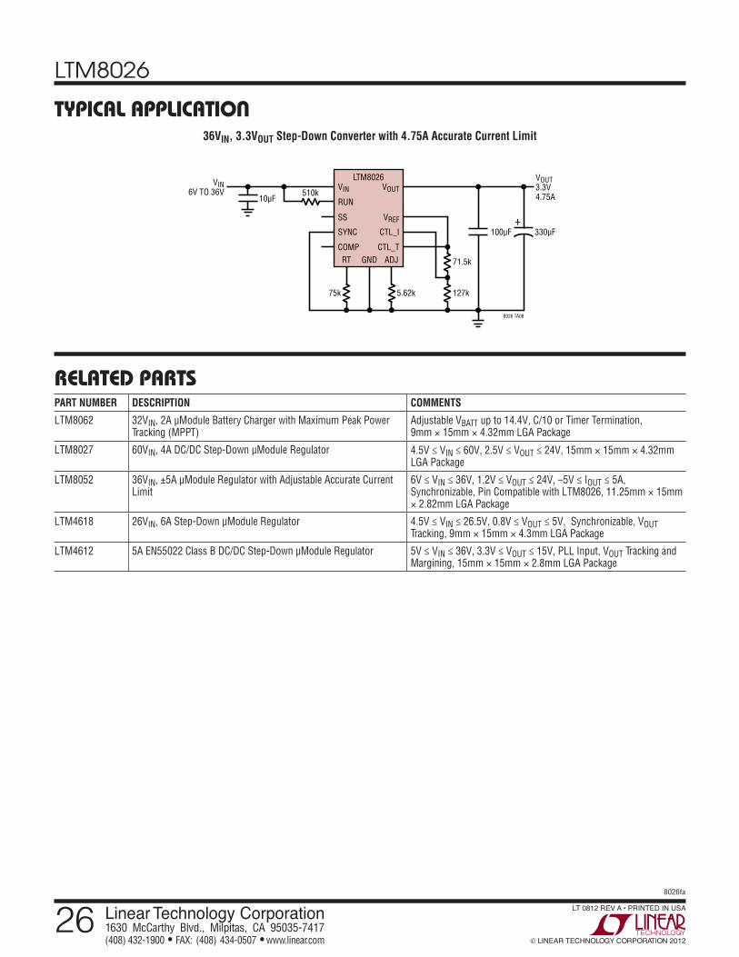
Typical applicaTion
PART NUMBER DESCRIPTION COMMENTS
LTM8062 32VIN, 2A µModule Battery Charger with Maximum Peak Power Tracking (MPPT)
Adjustable VBATT up to 14.4V, C/10 or Timer Termination, 9mm × 15mm × 4.32mm LGA Package
LTM8027 60VIN, 4A DC/DC Step-Down µModule Regulator 4.5V ≤ VIN ≤ 60V, 2.5V ≤ VOUT ≤ 24V, 15mm × 15mm × 4.32mm LGA Package
LTM8052 36VIN, ±5A µModule Regulator with Adjustable Accurate Current Limit
6V ≤ VIN ≤ 36V, 1.2V ≤ VOUT ≤ 24V, –5V ≤ IOUT ≤ 5A, Synchronizable, Pin Compatible with LTM8026, 11.25mm × 15mm × 2.82mm LGA Package
LTM4618 26VIN, 6A Step-Down µModule Regulator 4.5V ≤ VIN ≤ 26.5V, 0.8V ≤ VOUT ≤ 5V, Synchronizable, VOUT Tracking, 9mm × 15mm × 4.3mm LGA Package
LTM4612 5A EN55022 Class B DC/DC Step-Down µModule Regulator 5V ≤ VIN ≤ 36V, 3.3V ≤ VOUT ≤ 15V, PLL Input, VOUT Tracking and Margining, 15mm × 15mm × 2.8mm LGA Package
VIN
RUN
SS
LTM8026
SYNC 100µF 330µF
VOUT3.3V4.75A
8026 TA08
COMP
VOUT
VREF
CTL_I
CTL_TRT GND
75k 127k5.62k
71.5kADJ
10µF510k
VIN6V TO 36V
+
36VIN, 3.3VOUT Step-Down Converter with 4.75A Accurate Current Limit