Embed Size (px)
Citation preview
LTM2987
12987fa
For more information www.linear.com/LTM2987
Typical applicaTion
FeaTures DescripTion
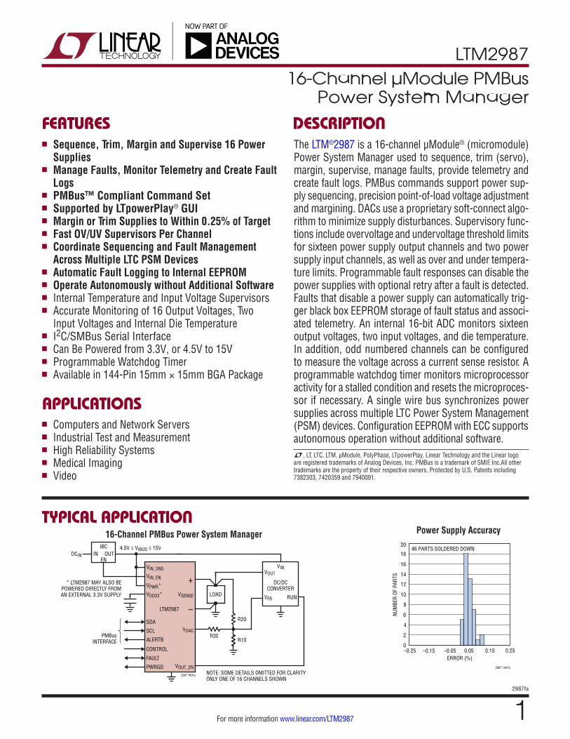
16-Channel µModule PMBus Power System Manager
16-Channel PMBus Power System Manager Power Supply Accuracy
The LTM®2987 is a 16-channel µModule® (micromodule) Power System Manager used to sequence, trim (servo), margin, supervise, manage faults, provide telemetry and create fault logs. PMBus commands support power sup-ply sequencing, precision point-of-load voltage adjustment and margining. DACs use a proprietary soft-connect algo-rithm to minimize supply disturbances. Supervisory func-tions include overvoltage and undervoltage threshold limits for sixteen power supply output channels and two power supply input channels, as well as over and under tempera-ture limits. Programmable fault responses can disable the power supplies with optional retry after a fault is detected. Faults that disable a power supply can automatically trig-ger black box EEPROM storage of fault status and associ-ated telemetry. An internal 16-bit ADC monitors sixteen output voltages, two input voltages, and die temperature. In addition, odd numbered channels can be configured to measure the voltage across a current sense resistor. A programmable watchdog timer monitors microprocessor activity for a stalled condition and resets the microproces-sor if necessary. A single wire bus synchronizes power supplies across multiple LTC Power System Management (PSM) devices. Configuration EEPROM with ECC supports autonomous operation without additional software.
applicaTions
n Sequence, Trim, Margin and Supervise 16 Power Supplies
n Manage Faults, Monitor Telemetry and Create Fault Logs
n PMBus™ Compliant Command Set n Supported by LTpowerPlay® GUI n Margin or Trim Supplies to Within 0.25% of Target n Fast OV/UV Supervisors Per Channel n Coordinate Sequencing and Fault Management
Across Multiple LTC PSM Devices n Automatic Fault Logging to Internal EEPROM n Operate Autonomously without Additional Software n Internal Temperature and Input Voltage Supervisors n Accurate Monitoring of 16 Output Voltages, Two
Input Voltages and Internal Die Temperature n I2C/SMBus Serial Interface n Can Be Powered from 3.3V, or 4.5V to 15V n Programmable Watchdog Timer n Available in 144-Pin 15mm × 15mm BGA Package
n Computers and Network Servers n Industrial Test and Measurement n High Reliability Systems n Medical Imaging n Video
L, LT, LTC, LTM, µModule, PolyPhase, LTpowerPlay, Linear Technology and the Linear logo are registered trademarks of Analog Devices, Inc. PMBus is a trademark of SMIF, Inc.All other trademarks are the property of their respective owners. Protected by U.S. Patents including 7382303, 7420359 and 7940091.
DCIN
R20
R10R30
LOAD
VOUT
VFB
VIN
RUN
DC/DCCONVERTER
VSENSE
VDAC
VOUT_EN
VIN_SNS
VPWR*
VDD33*
IBC
ENIN OUT
4.5V ≤ VIBUS ≤ 15V
FAULT
PWRGD
SDA
SCL
ALERTB
CONTROL
PMBusINTERFACE
NOTE: SOME DETAILS OMITTED FOR CLARITYONLY ONE OF 16 CHANNELS SHOWN
* LTM2987 MAY ALSO BEPOWERED DIRECTLY FROMAN EXTERNAL 3.3V SUPPLY
+
–LTM2987
VIN_EN
2987 TA01a
ERROR (%)–0.250
NUM
BER
OF P
ARTS
4
8
10
12
20
18
16
2987 TA01b
6
2
14
–0.05 0.25–0.15 0.05 0.15
46 PARTS SOLDERED DOWN
LTM2987
22987fa
For more information www.linear.com/LTM2987
pin conFiguraTionabsoluTe MaxiMuM raTingsSupply Voltages: VPWR...................................................... –0.3V to 15V VIN_SNS .................................................. –0.3V to 15V VDD33 .................................................... –0.3V to 3.6V VDD25 .................................................. –0.3V to 2.75VDigital Input/Output Voltages: ALERTB, SDA, SCL, CONTROL0, CONTROL1 ............................................ –0.3V to 5.5V PWRGD, SHARE_CLK, WDI/RESETB, WP ....................–0.3V to VDD33 + 0.3V FAULTB00, FAULTB01, FAULTB10, FAULTB11 ................................–0.3V to VDD33 + 0.3V ASEL0, ASEL1 ..........................–0.3V to VDD33 + 0.3VAnalog Voltages: REFP ................................................... –0.3V to 1.35V REFM .................................................... –0.3V to 0.3V VSENSEP[7:0] ............................................. –0.3V to 6V VSENSEM[7:0] ............................................. –0.3V to 6V VOUT_EN[3:0], VIN_EN ............................... –0.3V to 15V VOUT_EN[7:4] ............................................. –0.3V to 6V VDACP[7:0] ................................................. –0.3V to 6V VDACM[7:0] ............................................ –0.3V to 0.3VPull-Up Resistors: VPU ....................................................... –0.3V to 5.5V RPU1, RPU2, RPU3, RPU4 ........................ –0.3V to 5.5VOperating Junction Temperature Range: LTM2987C ............................................... 0°C to 70°C LTM2987I .......................................... –40°C to 105°CStorage Temperature Range ................ –55°C to 125°C*Maximum Junction Temperature ........................ 125°C*Maximum Solder Temperature .............................. 250°C*See OPERATION section of the LTC2977 data sheet for detailed EEPROM derating information for junction temperatures in excess of 105°C.
(Notes 1, 2, 3)
1
A
B
C
D
E
F
G
H
J
K
L
M
PIN 1 2 3 4 5 6 7TOP VIEW
BGA PACKAGE144-LEAD (15mm × 15mm × 3.42mm)
8 9 10 11 12
TJMAX = 125°C, θJA = 25.2°C/W, θJCtop = 15.6°C/W, θJCbottom = 7.1°C/W, θJB = 10.4°C/W,
WEIGHT = 1.6g, VALUES DETERMINED PER JEDEC 51-9, 51-12
orDer inForMaTionPART NUMBER PAD OR BALL FINISH PART MARKING* PACKAGE
TYPEMSL
RATINGOPERATING JUNCTION TEMPERATURE RANGEDEVICE FINISH CODE
LTM2987CY#PBF SAC305 (RoHS) LTM2987Y e1 BGA 3 0°C to 70°CLTM2987IY#PBF SAC305 (RoHS) LTM2987Y e1 BGA 3 –40°C to 105°C
Consult Marketing for parts specified with wider operating temperature ranges. *Device temperature grade is indicated by a label on the shipping container. Pad or ball finish code is per IPC/JEDEC J-STD-609.• Terminal Finish Part Marking:
www.linear.com/leadfree
• Recommended LGA and BGA PCB Assembly and Manufacturing Procedures: www.linear.com/umodule/pcbassembly
• LGA and BGA Package and Tray Drawings: www.linear.com/packaging
http://www.linear.com/product/LTM2987#orderinfo
LTM2987
32987fa
For more information www.linear.com/LTM2987
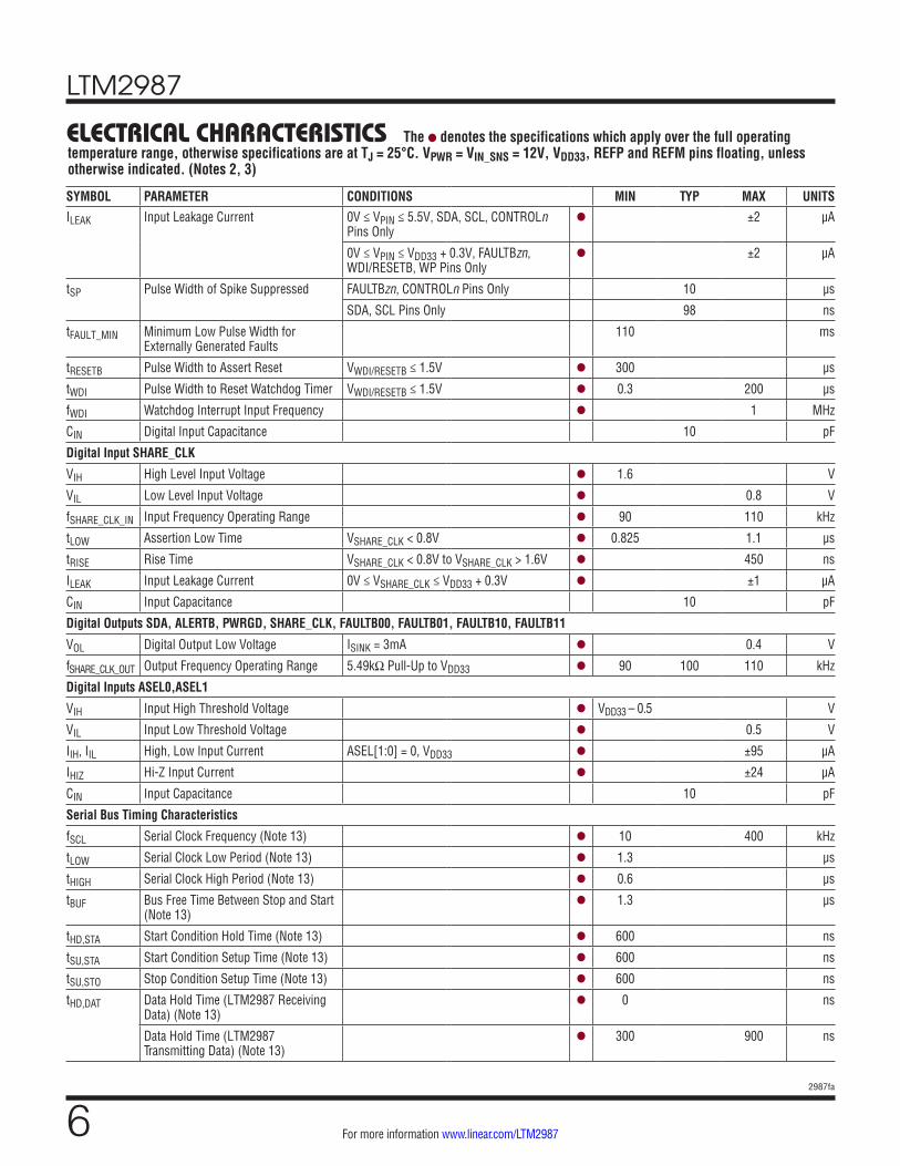
elecTrical characTerisTics The l denotes the specifications which apply over the full operating temperature range, otherwise specifications are at TJ = 25°C. VPWR = VIN_SNS = 12V, VDD33, REFP and REFM pins floating, unless otherwise indicated. (Notes 2, 3)
SYMBOL PARAMETER CONDITIONS MIN TYP MAX UNITSPower Supply Characteristics
VPWR VPWR Supply Input Operating Range l 4.5 15 V
IPWR VPWR Supply Current 4.5V ≤ VPWR ≤ 15V, VDD33 Floating l 10 13 mA
IVDD33 VDD33 Supply Current 3.13V ≤ VDD33 ≤ 3.47V, VPWR = VDD33 l 10 13 mA
VUVLO_VDD33 VDD33 Undervoltage Lockout VDD33 Ramping Up, VPWR = VDD33 l 2.35 2.55 2.8 V
VDD33 Undervoltage Lockout Hysteresis
120 mV
VDD33 Supply Input Operating Range VPWR = VDD33 l 3.13 3.47 V
Regulator Output Voltage 4.5V ≤ VPWR ≤ 15V l 3.13 3.26 3.47 V
Regulator Output Short-Circuit Current VPWR = 4.5V, VDD33 = 0V l 75 90 140 mA
VDD25 Regulator Output Voltage 3.13V ≤ VDD33 ≤ 3.47V l 2.35 2.5 2.6 V
Regulator Output Short-Circuit Current VPWR = VDD33 = 3.47V, VDD25 = 0V l 30 55 80 mA
tINIT Initialization Time Time from VIN Applied Until the TON_DELAY Timer Starts
30 ms
Voltage Reference Characteristics
VREF Output Voltage (Note 4) 1.232 V
Temperature Coefficient 3 ppm/°C
Hysteresis (Note 5) 100 ppm
ADC Characteristics
VIN_ADC Voltage Sense Input Range Differential Voltage: VIN_ADC = (VSENSEPn – VSENSEMn)
l 0 6 V
Single-Ended Voltage: VSENSEMn l –0.1 0.1 V
Current Sense Input Range (Odd Numbered Channels Only)
Single-Ended Voltage: VSENSEPn, VSENSEMn l –0.1 6 V
Differential Voltage: VIN_ADC l –170 170 mV
N_ADC Voltage Sense Resolution (Uses L16 Format)
0V ≤ VIN_ADC ≤ 6VMfr_config_adc_hires = 0
122 µV/LSB
Current Sense Resolution (Odd Numbered Channels Only)
0mV ≤ |VIN_ADC| < 16mV (Note 6) 16mV ≤ |VIN_ADC| < 32mV 32mV ≤ |VIN_ADC| < 63.9mV 63.9mV ≤ |VIN_ADC| < 127.9mV 127.9mV ≤ |VIN_ADC|Mfr_config_adc_hires = 1
15.625 31.25 62.5 125 250
µV/LSB µV/LSB µV/LSB µV/LSB µV/LSB
TUE_ADC_VOLT_SNS
Total Unadjusted Error (Note 4) Voltage Sense Mode VIN_ADC ≥ 1V l ±0.25 % of Reading
Voltage Sense Mode 0 ≤ VIN_ADC ≤ 1V l ±2.5 mV
TUE_ADC_CURR_SNS
Total Unadjusted Error (Note 4) Current Sense Mode, Odd Numbered Channels Only, 20mV ≤ VIN_ADC ≤ 170mV
l ±0.7 % of Reading
Current Sense Mode, Odd Numbered Channels Only, VIN_ADC ≤ 20mV
l ±140 µV
VOS_ADC Offset Error Current Sense Mode, Odd Numbered Channels Only
l ±35 µV
tCONV_ADC Conversion Time Voltage Sense Mode (Note 7) 6.15 ms
Current Sense Mode (Note 7) 24.6 ms
Temperature Input (Note 7) 24.6 ms
LTM2987
42987fa
For more information www.linear.com/LTM2987
elecTrical characTerisTics The l denotes the specifications which apply over the full operating temperature range, otherwise specifications are at TJ = 25°C. VPWR = VIN_SNS = 12V, VDD33, REFP and REFM pins floating, unless otherwise indicated. (Notes 2, 3)
SYMBOL PARAMETER CONDITIONS MIN TYP MAX UNITStUPDATE_ADC Update Time Odd Numbered Channels in Current Sense
Mode (Note 7)160 ms
CIN_ADC Input Sampling Capacitance 1 pF
fIN_ADC Input Sampling Frequency 62.5 kHz
IIN_ADC Input Leakage Current VIN_ADC = 0V, 0V ≤ VCOMMONMODE ≤ 6V, Current Sense Mode
l ±0.5 µA
Differential Input Current VIN_ADC = 0.17V, Current Sense Mode l 80 250 nA
VIN_ADC = 6V, Voltage Sense Mode l 10 15 µA
DAC Output Characteristics
N_VDACP Resolution 10 Bits
VFS_VDACP Full-Scale Output Voltage (Programmable)
DAC Code = 0x3FF DAC Polarity = 1
Buffer Gain Setting_0 Buffer Gain Setting_1
l
l
1.3 2.5
1.38 2.65
1.44 2.77
V V
INL_VDACP Integral Nonlinearity (Note 8) l ±2 LSB
DNL_VDACP Differential Nonlinearity (Note 8) l ±2.4 LSB
VOS_VDACP Offset Voltage (Note 8) l ±10 mV
VDACP Load Regulation (VDACPn – VDACMn) VDACPn = 2.65V, IVDACPn Sourcing = 2mA 100 ppm/mA
VDACPn = 0.1V, IVDACPn Sinking = 2mA 100 ppm/mA
PSRR (VDACPn – VDACMn) DC: 3.13V ≤ VDD33 ≤ 3.47V, VPWR = VDD33 60 dB
100mV Step in 20ns with 50pF Load 40 dB
DC CMRR (VDACPn – VDACMn) –0.1V ≤ VDACMn ≤ 0.1V 60 dB
Leakage Current VDACPn Hi-Z, 0V ≤ VDACPn ≤ 6V l ±100 nA
Short-Circuit Current Low VDACPn Shorted to GND l –10 –4 mA
Short-Circuit Current High VDACPn Shorted to VDD33 l 4 10 mA
COUT Output Capacitance VDACPn Hi-Z 10 pF
tS_VDACP DAC Output Update Rate Fast Servo Mode 500 µs
DAC Soft-Connect Comparator Characteristics
VOS_CMP Offset Voltage VDACPn = 0.2V l ±1 ±18 mV
VDACPn = 1.3V l ±2 ±26 mV
VDACPn = 2.65V l ±3 ±52 mV
Voltage Supervisor Characteristics
VIN_VS Input Voltage Range (Programmable) VIN_VS = (VSENSEPn – VSENSEMn)
Low Resolution Mode High Resolution Mode
l
l
0 0
6 3.8
V V
Single-Ended Voltage: VSENSEMn l –0.1 0.1 V
N_VS Voltage Sensing Resolution 0V to 3.8V Range: High Resolution Mode 4 mV/LSB
0V to 6V Range: Low Resolution Mode 8 mV/LSB
TUE_VS Total Unadjusted Error 2V ≤ VIN_VS ≤ 6V, Low Resolution Mode l ±1.25 % of Reading
1.5V < VIN_VS ≤ 3.8V, High Resolution Mode
l ±1.0 % of Reading
0.8V ≤ VIN_VS ≤ 1.5V, High Resolution Mode
l ±1.5 % of Reading
tS_VS Update Period 12.21 µs
LTM2987
52987fa
For more information www.linear.com/LTM2987
elecTrical characTerisTics The l denotes the specifications which apply over the full operating temperature range, otherwise specifications are at TJ = 25°C. VPWR = VIN_SNS = 12V, VDD33, REFP and REFM pins floating, unless otherwise indicated. (Notes 2, 3)
SYMBOL PARAMETER CONDITIONS MIN TYP MAX UNITSVIN_SNS Input Characteristics
VVIN_SNS VIN_SNS Input Voltage Range l 0 15 V
RVIN_SNS VIN_SNS Input Resistance l 70 90 110 kΩ
TUEVIN_SNS VIN_ON, VIN_OFF Threshold Total Unadjusted Error
3V ≤ VVIN_SNS ≤ 8V l ±2.0 % of Reading
VVIN_SNS > 8V l ±1.0 % of Reading
READ_VIN Total Unadjusted Error 3V ≤ VVIN_SNS ≤ 8V l ±1.5 % of Reading
VVIN_SNS > 8V l ±1.0 % of Reading
Temperature Sensor Characteristics
TUE_TS Total Unadjusted Error ±1 °C
VOUT Enable Output (VOUT_EN [3:0]) Characteristics
VVOUT_ENn Output High Voltage (Note 9) IVOUT_ENn = –5µA, VDD33 = 3.3V l 10 12.5 14.7 V
IVOUT_ENn Output Sourcing Current VVOUT_ENn Pull-Up Enabled, VVOUT_ENn = 1V l –5 –6 –8 µA
Output Sinking Current Strong Pull-Down Enabled, VVOUT_ENn = 0.4V
l 3 5 8 mA
Weak Pull-Down Enabled, VVOUT_ENn = 0.4V l 33 50 60 µA
Output Leakage Current Internal Pull-Up Disabled, 0V ≤ VVOUT_ENn ≤ 15V
l ±1 µA
VOUT Enable Output (VOUT_EN [7:4]) Characteristics
IVOUT_ENn Output Sinking Current Strong Pull-Down Enabled, VOUT_ENn = 0.1V
l 3 6 9 mA
Output Leakage Current 0V ≤ VVOUT_ENn ≤ 6V l ±1 µA
VIN Enable Output (VIN_EN) Characteristics
VVIN_EN Output High Voltage IVIN_EN = –5µA, VDD33 = 3.3V l 10 12.5 14.7 V
IVIN_EN Output Sourcing Current VIN_EN Pull-Up Enabled, VVIN_EN = 1V l –5 –6 –8 µA
Output Sinking Current VVIN_EN = 0.4V l 3 5 8 mA
Leakage Current Internal Pull-Up Disabled, 0V ≤ VVIN_EN ≤ 15V
l ±1 µA
EEPROM Characteristics
Endurance (Notes 10, 11) 0°C < TJ < 85°C During EEPROM Write Operations
l 10,000 Cycles
Retention (Notes 10, 11) TJ < 105°C l 20 Years
tMASS_WRITE Mass Write Operation Time (Note 12) STORE_USER_ALL, 0°C < TJ < 85°C During EEPROM Write Operations
l 440 4100 ms
General Purpose Pull-Up Resistors
RPU Pull-Up Resistance 10 kΩ
Digital Inputs SCL, SDA, CONTROL0, CONTROL1, WDI/RESETB, FAULTB00, FAULTB01, FAULTB10, FAULTB11, WP
VIH High Level Input Voltage l 2.1 V
VIL Low Level Input Voltage l 1.5 V
VHYST Input Hysteresis 20 mV
LTM2987
62987fa
For more information www.linear.com/LTM2987
elecTrical characTerisTics The l denotes the specifications which apply over the full operating temperature range, otherwise specifications are at TJ = 25°C. VPWR = VIN_SNS = 12V, VDD33, REFP and REFM pins floating, unless otherwise indicated. (Notes 2, 3)
SYMBOL PARAMETER CONDITIONS MIN TYP MAX UNITSILEAK Input Leakage Current 0V ≤ VPIN ≤ 5.5V, SDA, SCL, CONTROLn
Pins Onlyl ±2 µA
0V ≤ VPIN ≤ VDD33 + 0.3V, FAULTBzn, WDI/RESETB, WP Pins Only
l ±2 µA
tSP Pulse Width of Spike Suppressed FAULTBzn, CONTROLn Pins Only 10 µs
SDA, SCL Pins Only 98 ns
tFAULT_MIN Minimum Low Pulse Width for Externally Generated Faults
110 ms
tRESETB Pulse Width to Assert Reset VWDI/RESETB ≤ 1.5V l 300 µs
tWDI Pulse Width to Reset Watchdog Timer VWDI/RESETB ≤ 1.5V l 0.3 200 µs
fWDI Watchdog Interrupt Input Frequency l 1 MHz
CIN Digital Input Capacitance 10 pF
Digital Input SHARE_CLK
VIH High Level Input Voltage l 1.6 V
VIL Low Level Input Voltage l 0.8 V
fSHARE_CLK_IN Input Frequency Operating Range l 90 110 kHz
tLOW Assertion Low Time VSHARE_CLK < 0.8V l 0.825 1.1 µs
tRISE Rise Time VSHARE_CLK < 0.8V to VSHARE_CLK > 1.6V l 450 ns
ILEAK Input Leakage Current 0V ≤ VSHARE_CLK ≤ VDD33 + 0.3V l ±1 µA
CIN Input Capacitance 10 pF
Digital Outputs SDA, ALERTB, PWRGD, SHARE_CLK, FAULTB00, FAULTB01, FAULTB10, FAULTB11
VOL Digital Output Low Voltage ISINK = 3mA l 0.4 V
fSHARE_CLK_OUT Output Frequency Operating Range 5.49kΩ Pull-Up to VDD33 l 90 100 110 kHz
Digital Inputs ASEL0,ASEL1
VIH Input High Threshold Voltage l VDD33 – 0.5 V
VIL Input Low Threshold Voltage l 0.5 V
IIH, IIL High, Low Input Current ASEL[1:0] = 0, VDD33 l ±95 µA
IHIZ Hi-Z Input Current l ±24 µA
CIN Input Capacitance 10 pF
Serial Bus Timing Characteristics
fSCL Serial Clock Frequency (Note 13) l 10 400 kHz
tLOW Serial Clock Low Period (Note 13) l 1.3 µs
tHIGH Serial Clock High Period (Note 13) l 0.6 µs
tBUF Bus Free Time Between Stop and Start (Note 13)
l 1.3 µs
tHD,STA Start Condition Hold Time (Note 13) l 600 ns
tSU,STA Start Condition Setup Time (Note 13) l 600 ns
tSU,STO Stop Condition Setup Time (Note 13) l 600 ns
tHD,DAT Data Hold Time (LTM2987 Receiving Data) (Note 13)
l 0 ns
Data Hold Time (LTM2987 Transmitting Data) (Note 13)
l 300 900 ns
LTM2987
72987fa
For more information www.linear.com/LTM2987
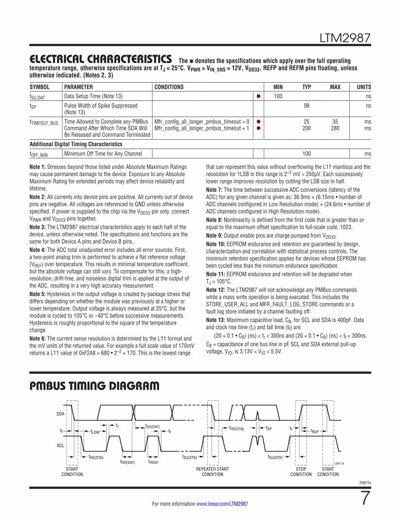
elecTrical characTerisTics The l denotes the specifications which apply over the full operating temperature range, otherwise specifications are at TJ = 25°C. VPWR = VIN_SNS = 12V, VDD33, REFP and REFM pins floating, unless otherwise indicated. (Notes 2, 3)
Note 1: Stresses beyond those listed under Absolute Maximum Ratings may cause permanent damage to the device. Exposure to any Absolute Maximum Rating for extended periods may affect device reliability and lifetime.Note 2: All currents into device pins are positive. All currents out of device pins are negative. All voltages are referenced to GND unless otherwise specified. If power is supplied to the chip via the VDD33 pin only, connect VPWR and VDD33 pins together.Note 3: The LTM2987 electrical characteristics apply to each half of the device, unless otherwise noted. The specifications and functions are the same for both Device A pins and Device B pins.Note 4: The ADC total unadjusted error includes all error sources. First, a two-point analog trim is performed to achieve a flat reference voltage (VREF) over temperature. This results in minimal temperature coefficient, but the absolute voltage can still vary. To compensate for this, a high-resolution, drift-free, and noiseless digital trim is applied at the output of the ADC, resulting in a very high accuracy measurement.Note 5: Hysteresis in the output voltage is created by package stress that differs depending on whether the module was previously at a higher or lower temperature. Output voltage is always measured at 25°C, but the module is cycled to 105°C or –40°C before successive measurements. Hysteresis is roughly proportional to the square of the temperature change. Note 6: The current sense resolution is determined by the L11 format and the mV units of the returned value. For example a full scale value of 170mV returns a L11 value of 0xF2A8 = 680 • 2–2 = 170. This is the lowest range
that can represent this value without overflowing the L11 mantissa and the resolution for 1LSB in this range is 2–2 mV = 250µV. Each successively lower range improves resolution by cutting the LSB size in half.Note 7: The time between successive ADC conversions (latency of the ADC) for any given channel is given as: 36.9ms + (6.15ms • number of ADC channels configured in Low Resolution mode) + (24.6ms • number of ADC channels configured in High Resolution mode).Note 8: Nonlinearity is defined from the first code that is greater than or equal to the maximum offset specification to full-scale code, 1023.Note 9: Output enable pins are charge pumped from VDD33.Note 10: EEPROM endurance and retention are guaranteed by design, characterization and correlation with statistical process controls. The minimum retention specification applies for devices whose EEPROM has been cycled less than the minimum endurance specification. Note 11: EEPROM endurance and retention will be degraded when TJ > 105°C. Note 12: The LTM2987 will not acknowledge any PMBus commands while a mass write operation is being executed. This includes the STORE_USER_ALL and MFR_FAULT_LOG_STORE commands or a fault log store initiated by a channel faulting off. Note 13: Maximum capacitive load, CB, for SCL and SDA is 400pF. Data and clock rise time (tr) and fall time (tf) are: (20 + 0.1 • CB) (ns) < tr < 300ns and (20 + 0.1 • CB) (ns) < tf < 300ns. CB = capacitance of one bus line in pF. SCL and SDA external pull-up voltage, VIO, is 3.13V < VIO < 5.5V.
SYMBOL PARAMETER CONDITIONS MIN TYP MAX UNITStSU,DAT Data Setup Time (Note 13) l 100 ns
tSP Pulse Width of Spike Suppressed (Note 13)
98 ns
tTIMEOUT_BUS Time Allowed to Complete any PMBus Command After Which Time SDA Will Be Released and Command Terminated
Mfr_config_all_longer_pmbus_timeout = 0 Mfr_config_all_longer_pmbus_timeout = 1
l
l
25 200
35 280
ms ms
Additional Digital Timing Characteristics
tOFF_MIN Minimum Off Time for Any Channel 100 ms
pMbus TiMing DiagraM
SDA
SCL
tHD(STA)tHD(DAT)
tSU(STA) tSU(STO)
tSU(DAT)tLOW
tHD(STA) tSP tBUF
STARTCONDITION
STOPCONDITION
REPEATED STARTCONDITION
STARTCONDITION
trtf
trtf
tHIGH 2987 TD
LTM2987
82987fa
For more information www.linear.com/LTM2987
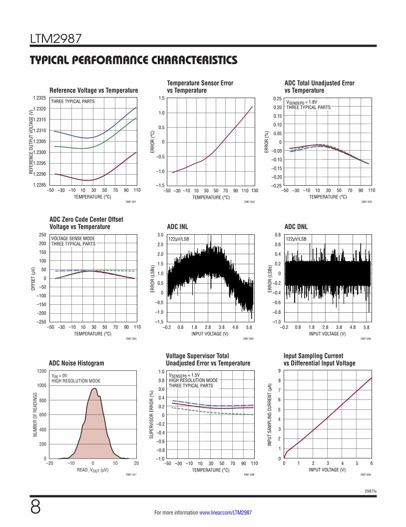
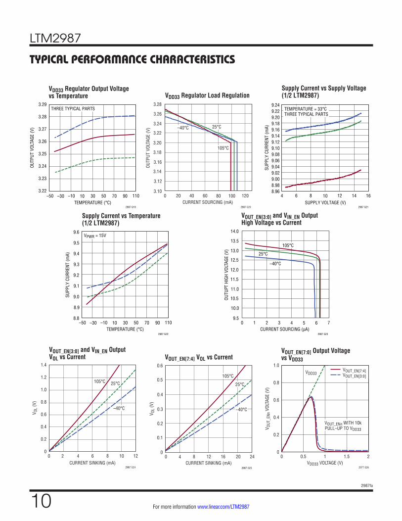
Typical perForMance characTerisTics
ADC Zero Code Center Offset Voltage vs Temperature ADC INL ADC DNL
ADC Noise HistogramVoltage Supervisor Total Unadjusted Error vs Temperature
Reference Voltage vs TemperatureTemperature Sensor Error vs Temperature
ADC Total Unadjusted Error vs Temperature
TEMPERATURE (°C)
REFE
RENC
E OU
TPUT
VOL
TAGE
(V)
1.2325
1.2320
1.2315
1.2310
1.2305
1.2300
1.2295
1.2290
1.2285
2987 G01
THREE TYPICAL PARTS
–50 5010 90 110–30 –10 30 70TEMPERATURE (°C)
–50–0.25
ERRO
R (%
)
–0.05
–0.10
–0.15
–0.20
0.05
0.10
0.15
0.25
50
2987 G03
0
0.20
10 90 110–30 –10 30 70
VSENSEP0 = 1.8VTHREE TYPICAL PARTS
TEMPERATURE (°C)
OFFS
ET (µ
V)
250
200
150
100
50
0
–50
–100
–150
–200
–250
2987 G04
VOLTAGE SENSE MODETHREE TYPICAL PARTS
–50 5010 90 110–30 –10 30 70INPUT VOLTAGE (V)
–0.2
ERRO
R (L
SBs)
5.8
3.0
2.5
2.0
1.5
1.0
0.5
0
–0.5
–1.0
–1.5
2987 G05
0.8 1.8 2.8 3.8 4.8
122µV/LSB
INPUT VOLTAGE (V)–0.2
ERRO
R (L
SBs)
5.8
0.8
0.6
0.4
0.2
0
–0.2
–0.4
–0.6
–0.8
–1.0
2987 G06
0.8 1.8 2.8 3.8 4.8
122µV/LSB
READ_VOUT (µV)–20
0
NUM
BER
OF R
EADI
NGS
200
400
600
800
1000
1200
–10 0 10 20
2987 G07
VIN = 0VHIGH RESOLUTION MODE
TEMPERATURE (°C)
SUPE
RVIS
OR E
RROR
(%)
2987 G08
–50–1.0
–0.2
–0.4
–0.6
–0.8
0.2
0
0.4
0.6
1.0
50
0.8
10 90 110–30 –10 30 70
VSENSEP0 = 1.5VHIGH RESOLUTION MODETHREE TYPICAL PARTS
Input Sampling Current vs Differential Input Voltage
INPUT VOLTAGE (V)0
0
INPU
T SA
MPL
ING
CURR
ENT
(µA)
1
3
4
5
4
9
2987 G09
2
21 53 6
6
7
8
TEMPERATURE (°C)
ERRO
R (°
C)
1.5
1.0
0.5
0
–0.5
–1.0
–1.5
2987 G02
–50 5010 90 110 130–30 –10 30 70
LTM2987
92987fa
For more information www.linear.com/LTM2987
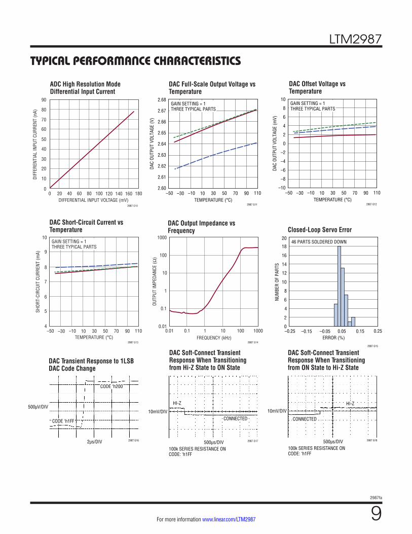
Typical perForMance characTerisTics
Closed-Loop Servo ErrorDAC Short-Circuit Current vs Temperature
DAC Output Impedance vs Frequency
DAC Transient Response to 1LSB DAC Code Change
ADC High Resolution Mode Differential Input Current
DAC Full-Scale Output Voltage vs Temperature
DAC Offset Voltage vs Temperature
DIFFERENTIAL INPUT VOLTAGE (mV)0
0
DIFF
EREN
TIAL
INPU
T CU
RREN
T (n
A)
10
30
40
50
120 140 160
90
2987 G10
20
6020 8040 100 180
60
70
80
TEMPERATURE (°C)
DAC
OUTP
UT V
OLTA
GE (V
)
2.68
2.67
2.66
2.65
2.64
2.63
2.62
2.61
2.60
2987 G11
–50 5010 90 110–30 –10 30 70
GAIN SETTING = 1THREE TYPICAL PARTS
TEMPERATURE (°C)
DAC
OUTP
UT V
OLTA
GE (m
V)
10
8
6
4
2
0
–2
–4
–6
–8
–10
2987 G12
–50 5010 90 110–30 –10 30 70
GAIN SETTING = 1THREE TYPICAL PARTS
500µV/DIV
2µs/DIV 2987 G16
CODE ‘h1FF
CODE ‘h200
10mV/DIV
500µs/DIV100k SERIES RESISTANCE ONCODE: ‘h1FF
2987 G17
HI-Z
CONNECTED
10mV/DIV
500µs/DIV100k SERIES RESISTANCE ONCODE: ‘h1FF
2987 G18
CONNECTED
HI-Z
DAC Soft-Connect Transient Response When Transitioning from ON State to Hi-Z State
DAC Soft-Connect Transient Response When Transitioning from Hi-Z State to ON State
TEMPERATURE (°C)
4
SHOR
T-CI
RCUI
T CU
RREN
T (m
A)
6
8
10
5
7
9
2987 G13
–50 5010 90 110–30 –10 30 70
GAIN SETTING = 1THREE TYPICAL PARTS
FREQUENCY (kHz)0.01
OUTP
UT IM
PEDA
NCE
(Ω)
10
100
1000
100
2987 G14
1
0.1
0.010.1 1 10 1000
ERROR (%)–0.250
NUM
BER
OF P
ARTS
4
8
10
12
20
18
16
2987 G15
6
2
14
–0.05 0.25–0.15 0.05 0.15
46 PARTS SOLDERED DOWN
LTM2987
102987fa
For more information www.linear.com/LTM2987
Typical perForMance characTerisTics
TEMPERATURE (°C)
OUTP
UT V
OLTA
GE (V
)
3.29
3.28
3.27
3.26
3.25
3.24
3.23
3.22
2987 G19
–50 5010 90 110–30 –10 30 70
THREE TYPICAL PARTS
CURRENT SOURCING (mA)0
3.10
OUTP
UT V
OLTA
GE (V
)
3.12
3.16
3.18
3.20
80
3.28
2987 G20
3.14
4020 10060 120
3.22
3.24
3.26
–40°C
105°C
25°C
SUPPLY VOLTAGE (V)4
SUPP
LY C
URRE
NT (m
A)
10 14
2987 G21
8.968.98
6 8 12
9.249.229.209.189.169.149.129.109.089.069.049.029.00
16
TEMPERATURE = 33°CTHREE TYPICAL PARTS
TEMPERATURE (°C)
8.8
SUPP
LY C
URRE
NT (m
A)
8.9
9.1
9.2
9.3
9.6
2987 G22
9.0
9.4
9.5
VPWR = 15V
–50 5010 90 110–30 –10 30 70CURRENT SOURCING (µA)
09.5
OUTU
PT H
IGH
VOLT
AGE
(V)
10.0
11.0
11.5
12.0
4
14.0
2987 G23
10.5
21 5 63 7
12.5
13.0
13.5105°C
25°C
–40°C
CURRENT SINKING (mA)0
1.4
1.2
1.0
0.8
0.6
0.4
0.2
06 10
2987 G24
2 4 8 12
V OL
(V)
105°C 25°C
–40°C
CURRENT SINKING (mA)0
0
V OL
(V)
0.1
0.2
0.3
0.4
0.6
4 8 12 16
2987 G25
20 24
0.5105°C
25°C
–40°C
VDD33
VOUT_ENn WITH 10kPULL–UP TO VDD33
VOUT_EN[7:4]VOUT_EN[3:0]
VDD33 VOLTAGE (V)0 0.5 1 1.5 2
0
0.2
0.4
0.6
0.8
1.0
V OUT
_ENn
VOL
TAGE
(V)
2977 G26
VDD33 Regulator Output Voltage vs Temperature VDD33 Regulator Load Regulation
VOUT_EN[3:0] and VIN_EN Output High Voltage vs Current
Supply Current vs Supply Voltage (1/2 LTM2987)
Supply Current vs Temperature (1/2 LTM2987)
VOUT_EN[7:4] VOL vs CurrentVOUT_EN[7:0] Output Voltage vs VDD33
VOUT_EN[3:0] and VIN_EN Output VOL vs Current
LTM2987
112987fa
For more information www.linear.com/LTM2987
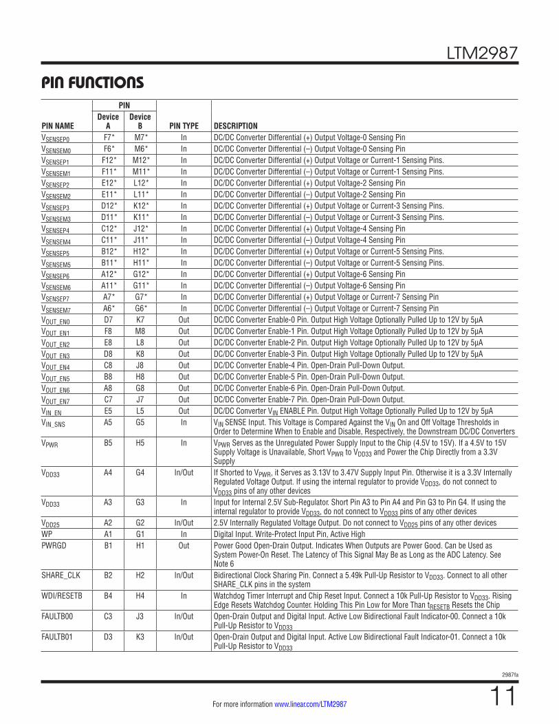
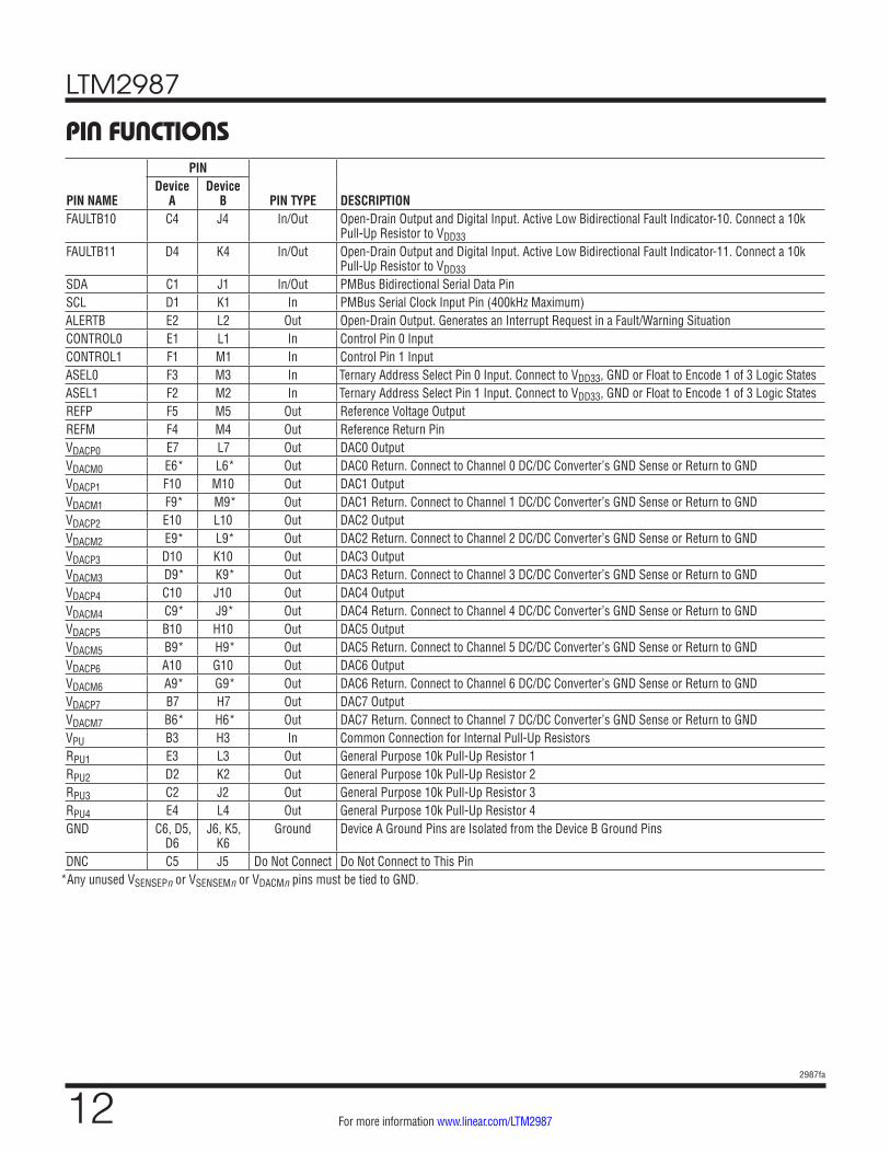
pin FuncTions
PIN NAME
PIN
PIN TYPE DESCRIPTIONDevice
ADevice
BVSENSEP0 F7* M7* In DC/DC Converter Differential (+) Output Voltage-0 Sensing PinVSENSEM0 F6* M6* In DC/DC Converter Differential (–) Output Voltage-0 Sensing PinVSENSEP1 F12* M12* In DC/DC Converter Differential (+) Output Voltage or Current-1 Sensing Pins.VSENSEM1 F11* M11* In DC/DC Converter Differential (–) Output Voltage or Current-1 Sensing Pins.VSENSEP2 E12* L12* In DC/DC Converter Differential (+) Output Voltage-2 Sensing PinVSENSEM2 E11* L11* In DC/DC Converter Differential (–) Output Voltage-2 Sensing PinVSENSEP3 D12* K12* In DC/DC Converter Differential (+) Output Voltage or Current-3 Sensing Pins.VSENSEM3 D11* K11* In DC/DC Converter Differential (–) Output Voltage or Current-3 Sensing Pins.VSENSEP4 C12* J12* In DC/DC Converter Differential (+) Output Voltage-4 Sensing PinVSENSEM4 C11* J11* In DC/DC Converter Differential (–) Output Voltage-4 Sensing PinVSENSEP5 B12* H12* In DC/DC Converter Differential (+) Output Voltage or Current-5 Sensing Pins.VSENSEM5 B11* H11* In DC/DC Converter Differential (–) Output Voltage or Current-5 Sensing Pins.VSENSEP6 A12* G12* In DC/DC Converter Differential (+) Output Voltage-6 Sensing PinVSENSEM6 A11* G11* In DC/DC Converter Differential (–) Output Voltage-6 Sensing PinVSENSEP7 A7* G7* In DC/DC Converter Differential (+) Output Voltage or Current-7 Sensing PinVSENSEM7 A6* G6* In DC/DC Converter Differential (–) Output Voltage or Current-7 Sensing PinVOUT_EN0 D7 K7 Out DC/DC Converter Enable-0 Pin. Output High Voltage Optionally Pulled Up to 12V by 5µAVOUT_EN1 F8 M8 Out DC/DC Converter Enable-1 Pin. Output High Voltage Optionally Pulled Up to 12V by 5µAVOUT_EN2 E8 L8 Out DC/DC Converter Enable-2 Pin. Output High Voltage Optionally Pulled Up to 12V by 5µAVOUT_EN3 D8 K8 Out DC/DC Converter Enable-3 Pin. Output High Voltage Optionally Pulled Up to 12V by 5µAVOUT_EN4 C8 J8 Out DC/DC Converter Enable-4 Pin. Open-Drain Pull-Down Output.VOUT_EN5 B8 H8 Out DC/DC Converter Enable-5 Pin. Open-Drain Pull-Down Output.VOUT_EN6 A8 G8 Out DC/DC Converter Enable-6 Pin. Open-Drain Pull-Down Output.VOUT_EN7 C7 J7 Out DC/DC Converter Enable-7 Pin. Open-Drain Pull-Down Output.VIN_EN E5 L5 Out DC/DC Converter VIN ENABLE Pin. Output High Voltage Optionally Pulled Up to 12V by 5µAVIN_SNS A5 G5 In VIN SENSE Input. This Voltage is Compared Against the VIN On and Off Voltage Thresholds in
Order to Determine When to Enable and Disable, Respectively, the Downstream DC/DC ConvertersVPWR B5 H5 In VPWR Serves as the Unregulated Power Supply Input to the Chip (4.5V to 15V). If a 4.5V to 15V
Supply Voltage is Unavailable, Short VPWR to VDD33 and Power the Chip Directly from a 3.3V Supply
VDD33 A4 G4 In/Out If Shorted to VPWR, it Serves as 3.13V to 3.47V Supply Input Pin. Otherwise it is a 3.3V Internally Regulated Voltage Output. If using the internal regulator to provide VDD33, do not connect to VDD33 pins of any other devices
VDD33 A3 G3 In Input for Internal 2.5V Sub-Regulator. Short Pin A3 to Pin A4 and Pin G3 to Pin G4. If using the internal regulator to provide VDD33, do not connect to VDD33 pins of any other devices
VDD25 A2 G2 In/Out 2.5V Internally Regulated Voltage Output. Do not connect to VDD25 pins of any other devicesWP A1 G1 In Digital Input. Write-Protect Input Pin, Active HighPWRGD B1 H1 Out Power Good Open-Drain Output. Indicates When Outputs are Power Good. Can be Used as
System Power-On Reset. The Latency of This Signal May Be as Long as the ADC Latency. See Note 6
SHARE_CLK B2 H2 In/Out Bidirectional Clock Sharing Pin. Connect a 5.49k Pull-Up Resistor to VDD33. Connect to all other SHARE_CLK pins in the system
WDI/RESETB B4 H4 In Watchdog Timer Interrupt and Chip Reset Input. Connect a 10k Pull-Up Resistor to VDD33. Rising Edge Resets Watchdog Counter. Holding This Pin Low for More Than tRESETB Resets the Chip
FAULTB00 C3 J3 In/Out Open-Drain Output and Digital Input. Active Low Bidirectional Fault Indicator-00. Connect a 10k Pull-Up Resistor to VDD33
FAULTB01 D3 K3 In/Out Open-Drain Output and Digital Input. Active Low Bidirectional Fault Indicator-01. Connect a 10k Pull-Up Resistor to VDD33
LTM2987
122987fa
For more information www.linear.com/LTM2987
pin FuncTions
PIN NAME
PIN
PIN TYPE DESCRIPTIONDevice
ADevice
BFAULTB10 C4 J4 In/Out Open-Drain Output and Digital Input. Active Low Bidirectional Fault Indicator-10. Connect a 10k
Pull-Up Resistor to VDD33FAULTB11 D4 K4 In/Out Open-Drain Output and Digital Input. Active Low Bidirectional Fault Indicator-11. Connect a 10k
Pull-Up Resistor to VDD33SDA C1 J1 In/Out PMBus Bidirectional Serial Data PinSCL D1 K1 In PMBus Serial Clock Input Pin (400kHz Maximum)ALERTB E2 L2 Out Open-Drain Output. Generates an Interrupt Request in a Fault/Warning SituationCONTROL0 E1 L1 In Control Pin 0 InputCONTROL1 F1 M1 In Control Pin 1 InputASEL0 F3 M3 In Ternary Address Select Pin 0 Input. Connect to VDD33, GND or Float to Encode 1 of 3 Logic StatesASEL1 F2 M2 In Ternary Address Select Pin 1 Input. Connect to VDD33, GND or Float to Encode 1 of 3 Logic StatesREFP F5 M5 Out Reference Voltage OutputREFM F4 M4 Out Reference Return PinVDACP0 E7 L7 Out DAC0 OutputVDACM0 E6* L6* Out DAC0 Return. Connect to Channel 0 DC/DC Converter’s GND Sense or Return to GNDVDACP1 F10 M10 Out DAC1 OutputVDACM1 F9* M9* Out DAC1 Return. Connect to Channel 1 DC/DC Converter’s GND Sense or Return to GNDVDACP2 E10 L10 Out DAC2 OutputVDACM2 E9* L9* Out DAC2 Return. Connect to Channel 2 DC/DC Converter’s GND Sense or Return to GNDVDACP3 D10 K10 Out DAC3 OutputVDACM3 D9* K9* Out DAC3 Return. Connect to Channel 3 DC/DC Converter’s GND Sense or Return to GNDVDACP4 C10 J10 Out DAC4 OutputVDACM4 C9* J9* Out DAC4 Return. Connect to Channel 4 DC/DC Converter’s GND Sense or Return to GNDVDACP5 B10 H10 Out DAC5 OutputVDACM5 B9* H9* Out DAC5 Return. Connect to Channel 5 DC/DC Converter’s GND Sense or Return to GNDVDACP6 A10 G10 Out DAC6 OutputVDACM6 A9* G9* Out DAC6 Return. Connect to Channel 6 DC/DC Converter’s GND Sense or Return to GNDVDACP7 B7 H7 Out DAC7 OutputVDACM7 B6* H6* Out DAC7 Return. Connect to Channel 7 DC/DC Converter’s GND Sense or Return to GNDVPU B3 H3 In Common Connection for Internal Pull-Up ResistorsRPU1 E3 L3 Out General Purpose 10k Pull-Up Resistor 1RPU2 D2 K2 Out General Purpose 10k Pull-Up Resistor 2RPU3 C2 J2 Out General Purpose 10k Pull-Up Resistor 3RPU4 E4 L4 Out General Purpose 10k Pull-Up Resistor 4GND C6, D5,
D6J6, K5,
K6Ground Device A Ground Pins are Isolated from the Device B Ground Pins
DNC C5 J5 Do Not Connect Do Not Connect to This Pin*Any unused VSENSEPn or VSENSEMn or VDACMn pins must be tied to GND.
LTM2987
132987fa
For more information www.linear.com/LTM2987
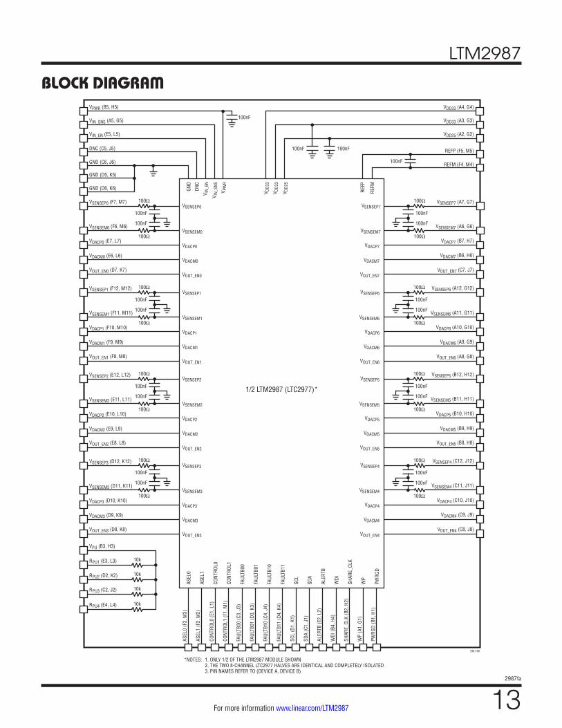
block DiagraM
CONT
ROL0
(E1,
L1)
CONT
ROL1
(F1,
M1)
SHAR
E_CL
K (B
2, H
2)
GND
ASEL
0
DNC
V IN_
EN
V IN_
SNS
V PW
R
GND (C6, J6)
DNC (C5, J5)
VIN_EN (E5, L5)
VIN_SNS (A5, G5)
VPWR (B5, H5)
GND (D5, K5)
GND (D6, K6)
VSENSEP0
VSENSEM0
VSENSEP7
VSENSEM7
VSENSEP0 (F7, M7)
VSENSEM0 (F6, M6)
VDACP0VDACP0 (E7, L7)
VDACM0VDACM0 (E6, L6)
VOUT_EN0VOUT_EN0 (D7, K7)
ASEL
0 (F
3, M
3)
VSENSEP1
VSENSEM1
VSENSEP1 (F12, M12)
VSENSEM1 (F11, M11)
VDACP1VDACP1 (F10, M10)
VDACM1VDACM1 (F9, M9)
VOUT_EN1VOUT_EN1 (F8, M8)
VSENSEP2
VSENSEM2
1/2 LTM2987 (LTC2977)*
VSENSEP2 (E12, L12)
VSENSEM2 (E11, L11)
VDACP2VDACP2 (E10, L10)
VDACM2VDACM2 (E9, L9)
VOUT_EN2VOUT_EN2 (E8, L8)
VSENSEP3
VSENSEM3
VSENSEP3 (D12, K12)
VSENSEM3 (D11, K11)
VDACP3VDACP3 (D10, K10)
VDACM3VDACM3 (D9, K9)
VOUT_EN3
*NOTES: 1. ONLY 1/2 OF THE LTM2987 MODULE SHOWN 2. THE TWO 8-CHANNEL LTC2977 HALVES ARE IDENTICAL AND COMPLETELY ISOLATED 3. PIN NAMES REFER TO (DEVICE A, DEVICE B)
VDACP7
VDACM7
VOUT_EN7
VSENSEP6
VSENSEM6
VDACP6
VDACM6
VOUT_EN6
VSENSEP5
VSENSEM5
VDACP5
VDACM5
VOUT_EN5
VSENSEP4
VSENSEM4
VDACP4
VDACM4
VOUT_EN4
2987 BD
VOUT_EN3 (D8, K8)
10k
VPU (B3, H3)
RPU1 (E3, L3)
RPU2 (D2, K2)
RPU3 (C2, J2)
RPU4 (E4, L4)
VSENSEP7 (A7, G7)
VDD33 (A4, G4)
VDD33 (A3, G3)
VDD25 (A2, G2)
REFP (F5, M5)
REFM (F4, M4)
VSENSEM7 (A6, G6)
VDACP7 (B7, H7)
VDACM7 (B6, H6)
VOUT_EN7 (C7, J7)
VSENSEP6 (A12, G12)
VSENSEM6 (A11, G11)
VDACP6 (A10, G10)
VDACM6 (A9, G9)
VOUT_EN6 (A8, G8)
VSENSEP5 (B12, H12)
VSENSEM5 (B11, H11)
VDACP5 (B10, H10)
VDACM5 (B9, H9)
VOUT_EN5 (B8, H8)
VSENSEP4 (C12, J12)
VSENSEM4 (C11, J11)
VDACP4 (C10, J10)
VDACM4 (C9, J9)
VOUT_EN4 (C8, J8)
V DD3
3
V DD3
3
V DD2
5
REFP
REFM
ASEL
1AS
EL1
(F2,
M2)
CONT
ROL0
CONT
ROL1
FAUL
TB00
FAUL
TB00
(C3,
J3)
FAUL
TB01
FAUL
TB01
(D3,
K3)
FAUL
TB10
FAUL
TB10
(C4,
J4)
FAUL
TB11
FAUL
TB11
(D4,
K4)
SCL
SCL
(D1,
K1)
SDA
SDA
(C1,
J1)
ALER
TBAL
ERTB
(E2,
L2)
WDI
WDI
(B4,
H4)
SHAR
E_CL
K
WP
WP
(A1,
G1)
PWRG
DPW
RGD
(B1,
H1)
10k
10k
10k
100Ω
100Ω
100nF
100nF
100Ω
100Ω
100nF
100nF
100Ω
100Ω
100nF
100nF
100Ω
100Ω
100nF
100nF
100nF
100nF 100nF
100nF
100Ω
100Ω
100nF
100nF
100Ω
100Ω
100nF
100nF
100Ω
100Ω
100nF
100nF
100Ω
100Ω
100nF
100nF
LTM2987
142987fa
For more information www.linear.com/LTM2987
operaTionOverview
The LTM2987 contains two independent LTC2977 devices and most of the passive components required to make a complete 16-channel power system manager. The LTM2987 simplifies power system design by integrating the required passive components, reducing the bill-of-materials and improving PC board routing efficiency.
Each half of the LTM2987 behaves the same as a stand-alone LTC2977 including independent power supply and ground pins. This feature can be used to increase redun-dancy in a system while keeping the overall solution size small.
Refer to the LTC2977 data sheet for a detailed description of the device operation, the PMBus command set, and applications information.
Device Address
Since the LTM2987 consists of two independent LTC2977 devices, each half of the LTM2987 must be configured for a unique address. The I2C/SMBus addresses of the LTM2987 are configured in the same manner as for indi-vidual LTC2977 devices. The LTM2987 also responds to the LTC2977 global address and the SMBus Alert Response address, regardless of the state of the ASEL pins and the MFR_I2C_BASE_ADDRESS register. Please refer to the Device Address section in the LTC2977 data sheet for more details.
MFR_SPECIAL_ID
The LTM2987 contains unique MFR_SPECIAL_ID val-ues to differentiate it from the LTC2977. Table 1 lists the MFR_SPECIAL_ID values for the LTM2987.
Table 1. LTM2987 MFR_SPECIAL_ID Values
LTM2987 DEVICE MFR_SPECIAL_ID
Device A 0x8011
Device B 0x8021
LTM2987
152987fa
For more information www.linear.com/LTM2987
applicaTions inForMaTion
Figure 3. Undedicated Pull-Up Resistors
10k
VPU
RPU1
1/2 LTM2987
2987 F03
10kRPU2
10kRPU3
10kRPU4
OVERVIEW
The LTM2987 is a Power System Manager that is capable of sequencing, margining, trimming, super-vising output voltage for OV/UV conditions, providing fault management, and voltage readback for sixteen DC/DC converters. Input voltage and LTM2987 junction temperature readback are also available. Odd numbered channels can be configured to read back current sense resistor voltages. Multiple LTM2987s can be synchro-nized to operate in unison using the SHARE_CLK, FAULTB and CONTROL pins. The LTM2987 utilizes a PMBus com-pliant interface and command set.
Alternatively, power from an external 3.3V supply may be applied directly to the VDD33 pins using a voltage between 3.13V and 3.47V. Tie VPWR to the VDD33 pins. See Figure 2. In this case, VDD33(A) and VDD33(B) may be tied together. All functionality is available when using this alternate power method. The higher voltages needed for the VOUT_EN[0:3] pins and bias for the VSENSE pins are charge pumped from VDD33.
The method used to power each device in the LTM2987 is independent of the other device. Either method may be used in any combination.
APPLICATION CIRCUITS
Undedicated Pull-Up Resistors
Each half of the LTM2987 module has four undedicated 10k pull-up resistors as shown in Figure 3. The common pull-up voltage is applied to the VPU pin, and the individual pull-up resistors are on RPU1, RPU2, RPU3 and RPU4. These pull-up resistors can be used for the open-drain pins such as SDA, SCL, ALERTB or FAULTBzn in which case the common pull-up voltage VPU should be connected to a 3.3V supply. To simplify the layout, the pin VPU is adjacent to the VDD33 pin.
Anti-Aliasing Filter Considerations
Since most of the passive components required for opera-tion are integrated into the LTM2987, no external filter components are required.
Figure 1. Powering LTM2987 Directly from an Intermediate Bus
Figure 2. Powering LTM2987 from External 3.3V Supply
VPWR
VIN_SNS
VDD33
VDD33
VDD25
VPWR
VIN_SNS
VDD33
VDD33
VDD25
LTM2987*DEVICE A
4.5V < VPWRA < 15V
GND *SOME DETAILS OMITTED FOR CLARITY
2987 F01
4.5V < VPWRB < 15V
LTM2987*DEVICE B
GND
VPWR
VDD33
VDD33
VDD25
VPWR
VDD33
VDD33
VDD25
LTM2987*DEVICE A
EXTERNAL 3.3V
GND *SOME DETAILS OMITTED FOR CLARITY
2987 F02
EXTERNAL 3.3V
LTM2987*DEVICE B
GND
POWERING THE LTM2987
The LTM2987 can be powered two ways. The first method requires that a voltage between 4.5V and 15V be applied to the VPWR pin. See Figure 1. Internal linear regulators convert VPWR down to 3.3V which drives all of the inter-nal circuitry in each device. Do not tie the VDD33(A) and VDD33(B) pins together since each half of the LTM2987 has independent voltage regulators.
LTM2987
162987fa
For more information www.linear.com/LTM2987
100k
100k
VSENSEP
VSENSEM
LTM2987
2987 F04
Figure 4. Connecting Unused Inputs to GND
applicaTions inForMaTionVIN Sense
Voltages other than VIN can be monitored and supervised using the VIN_SNS pins. Each VIN_SNS pin has a calibrated internal divider allowing it to directly sense voltages up to 15V.
Unused ADC Sense Inputs
Connect all unused ADC sense inputs (VSENSEPn or VSENSEMn) to GND. In a system where the inputs are con-nected to removable cards and may be left floating in certain situations, connect the inputs to GND using 100k resistors, as shown in Figure 4.
Output Enablesn Use appropriate pull-up resistors on all VOUT_ENn pins.n Verify that the absolute maximum ratings of the VOUT_
ENn pins are not exceeded.
VIN Sensen No external resistive divider is required to sense VIN;
VIN_SNS already has an internal calibrated divider.
Logic Signalsn Verify the absolute maximum ratings of the digital pins
(SCL, SDA, ALERTB, FAULTBzn, CONTROLn, SHARE_CLK, WDI, ASELn, PWRGD) are not exceeded.
n Connect all SHARE_CLK pins in the system together and pull up to 3.3V with a 5.49k resistor.
n Do not leave CONTROLn pins floating. Pull up to 3.3V with a 10k resistor.
n Tie WDI/RESETB to VDD33 with a 10k resistor. Do not connect a capacitor to the WDI/RESETB pin.
n Tie WP to either VDD33 or GND. Do not leave floating.
Unused Inputsn Connect all unused VSENSEPn, VSENSEMn and DACMn
pins to GND. Do not float unused inputs. Refer to Unused ADC Sense Inputs in the Applications Information section of the LTC2977 data sheet.
DAC Outputsn Select appropriate resistor for desired margin range.
Refer to the resistor selection tool in LTpowerPlay for assistance.
Power Suppliesn If powered from VPWR, do not connect the VDD33(A)
and VDD33(B) pins together. Each VDD33 pin has an inde-pendent, internal regulator.
For a more complete list of design considerations and a schematic checklist, see the Design Checklist on the LTM2987 product page: www.linear.com/LTM2987.
PCB ASSEMBLY AND LAYOUT SUGGESTIONS
Bypass Capacitor Placement
All required bypass capacitors are integrated into the LTM2987. No additional bypass capacitance is required. The PCB layout should adhere to good layout guidelines. A multilayer PCB that dedicates a layer to power and ground is recommended. Low resistance and low inductance power and ground connections are important to minimize power supply noise and ensure proper device operation.
DESIGN CHECKLIST
I2Cn Each half of the LTM2987 must be configured for a
unique address. Unique hardware ASELn values are recommended for simplest in system programming.
n The address select pins (ASELn) are tri-level; Check Table 1 of the LTC2977 data sheet.
n Check addresses for collision with other devices on the bus and any global addresses.
LTM2987
172987fa
For more information www.linear.com/LTM2987
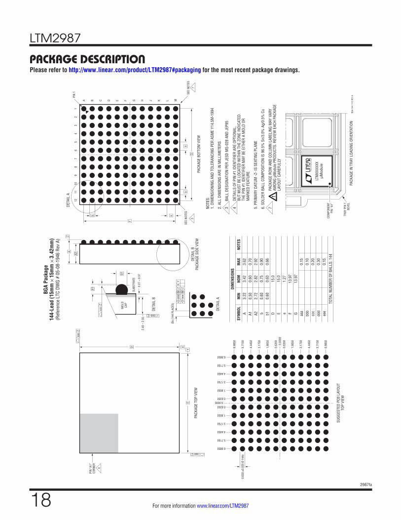
package DescripTionLTM2987 Component BGA Pinout (Top View)
1 2 3 4 5 6 7 8 9 10 11 12
Devi
ce A
A WP VDD25 VDD33 VDD33 VIN_SNS VSENSEM7 VSENSEP7 VOUT_EN6 VDACM6 VDACP6 VSENSEM6 VSENSEP6
B PWRGD SHARE_CLK VPU WDI VPWR VDACM7 VDACP7 VOUT_EN5 VDACM5 VDACP5 VSENSEM5 VSENSEP5
C SDA RPU3 FAULTB00 FAULTB10 DNC GND VOUT_EN7 VOUT_EN4 VDACM4 VDACP4 VSENSEM4 VSENSEP4
D SCL RPU2 FAULTB01 FAULTB11 GND GND VOUT_EN0 VOUT_EN3 VDACM3 VDACP3 VSENSEM3 VSENSEP3
E CONTROL0 ALERTB RPU1 RPU4 VIN_EN VDACM0 VDACP0 VOUT_EN2 VDACM2 VDACP2 VSENSEM2 VSENSEP2
F CONTROL1 ASEL1 ASEL0 REFM REFP VSENSEM0 VSENSEP0 VOUT_EN1 VDACM1 VDACP1 VSENSEM1 VSENSEP1
Devi
ce B
G WP VDD25 VDD33 VDD33 VIN_SNS VSENSEM7 VSENSEP7 VOUT_EN6 VDACM6 VDACP6 VSENSEM6 VSENSEP6
H PWRGD SHARE_CLK VPU WDI VPWR VDACM7 VDACP7 VOUT_EN5 VDACM5 VDACP5 VSENSEM5 VSENSEP5
J SDA RPU3 FAULTB00 FAULTB10 DNC GND VOUT_EN7 VOUT_EN4 VDACM4 VDACP4 VSENSEM4 VSENSEP4
K SCL RPU2 FAULTB01 FAULTB11 GND GND VOUT_EN0 VOUT_EN3 VDACM3 VDACP3 VSENSEM3 VSENSEP3
L CONTROL0 ALERTB RPU1 RPU4 VIN_EN VDACM0 VDACP0 VOUT_EN2 VDACM2 VDACP2 VSENSEM2 VSENSEP2
M CONTROL1 ASEL1 ASEL0 REFM REFP VSENSEM0 VSENSEP0 VOUT_EN1 VDACM1 VDACP1 VSENSEM1 VSENSEP1
LTM2987
182987fa
For more information www.linear.com/LTM2987
package DescripTionPlease refer to http://www.linear.com/product/LTM2987#packaging for the most recent package drawings.
4
PIN
“A1”
CORN
ER
NOTE
S:1.
DIM
ENSI
ONIN
G AN
D TO
LERA
NCIN
G PE
R AS
ME
Y14.
5M-1
994
2. A
LL D
IMEN
SION
S AR
E IN
MIL
LIM
ETER
S
BAL
L DE
SIGN
ATIO
N PE
R JE
SD M
S-02
8 AN
D JE
P95
5. P
RIM
ARY
DATU
M -Z
- IS
SEAT
ING
PLAN
E
6. S
OLDE
R BA
LL C
OMPO
SITI
ON IS
96.
5% S
n/3.
0% A
g/0.
5% C
u
43
DETA
ILS
OF P
IN #
1 ID
ENTI
FIER
ARE
OPT
IONA
L,BU
T M
UST
BE L
OCAT
ED W
ITHI
N TH
E ZO
NE IN
DICA
TED.
THE
PIN
#1 ID
ENTI
FIER
MAY
BE
EITH
ER A
MOL
D OR
M
ARKE
D FE
ATUR
E
PACK
AGE
TOP
VIEW
X
Y
aaa
Z
aaa Z
PACK
AGE
BOTT
OM V
IEW
3
SEE
NOTE
S
SUGG
ESTE
D PC
B LA
YOUT
TOP
VIEW
BGA
144
1113
REV
A
LTM
XXXX
XXµM
odul
e
TRAY
PIN
1BE
VEL
PACK
AGE
IN T
RAY
LOAD
ING
ORIE
NTAT
ION
COM
PONE
NTPI
N “A
1”DETA
IL A
PIN
1
0.0000
0.00
00
DETA
IL A
Øb (1
44 P
LACE
S)
DETA
IL B
SUBS
TRAT
E
0.27
– 0
.37
2.45
– 2
.55
// bbb Z
D
A
A1
b1
ccc
Z
DETA
IL B
PACK
AGE
SIDE
VIE
W
MOL
DCA
P
Z
MX
YZ
ddd
MZ
eee
0.63
0 ±0
.025
Ø 1
44x
SYM
BOL
A A1 A2 b b1 D E e F G aaa
bbb
ccc
ddd
eee
MIN
3.22
0.50
2.72
0.60
0.60
NOM
3.42
0.60
2.82
0.75
0.63
15.0
15.0
1.27
13.9
713
.97
MAX
3.62
0.70
2.92
0.90
0.66
0.15
0.10
0.20
0.30
0.15
NOTE
S
DIM
ENSI
ONS
TOTA
L NU
MBE
R OF
BAL
LS: 1
44
Eb
e
e
b
A2
F
G
BGA
Pack
age
144-
Lead
(15m
m ×
15m
m ×
3.4
2mm
)(R
efer
ence
LTC
DW
G #
05-0
8-19
46 R
ev A
)
0.63
50
0.63
50
1.90
50
1.90
50
3.17
50
3.17
50
4.44
50
4.44
50
5.71
50
5.71
50
6.98
50
6.9850
6.9850
5.7150
5.7150
4.4450
4.4450
3.1750
3.1750
1.9050
1.9050
0.6350
0.6350
6.98
50
GFEA B DC H MLKJ
21
43
56
712
89
1011
7PA
CKAG
E RO
W A
ND C
OLUM
N LA
BELI
NG M
AY V
ARY
AMON
G µM
odul
e PR
ODUC
TS. R
EVIE
W E
ACH
PACK
AGE
LAYO
UT C
AREF
ULLY
!
7
SEE
NOTE
S
LTM2987
192987fa
For more information www.linear.com/LTM2987
Information furnished by Linear Technology Corporation is believed to be accurate and reliable. However, no responsibility is assumed for its use. Linear Technology Corporation makes no representa-tion that the interconnection of its circuits as described herein will not infringe on existing patent rights.
revision hisToryREV DATE DESCRIPTION PAGE NUMBER
A 08/16 Added EEPROM ECC information and updated Typical ApplicationIncreased Maximum Solder Temperature from 245°C to 250°CUpdated DAC Output Update Rate (tS_VDACP) to 500µs from 250µsAdded Note 4Added graph: VOUT_EN[7:0] Output Voltage vs VDD33
Updated VDD33 and SHARE_CLK pin functionsChanged MFR_SPECIAL_ID in Table 1
1247
101114
LTM2987
202987fa
For more information www.linear.com/LTM2987 LINEAR TECHNOLOGY CORPORATION 2014
LT 0816 REV A • PRINTED IN USAwww.linear.com/LTC2987
relaTeD parTs
Typical applicaTion
PART NUMBER DESCRIPTION COMMENTSLTC2970 Dual I2C Power Supply Monitor and Margining Controller 5V to 15V, 0.5% TUE 14-Bit ADC, 8-Bit DAC, Temperature SensorLTC2974 4-Channel PMBus Power System Manager 0.25% TUE 16-Bit ADC, Voltage/Current/Temperature Monitoring/SupervisionLTC2975 4-Channel PMBus Power System Manager LTC2974 Plus Input Current, Power and Energy AccumulatorLTC2977 8-Channel PMBus Power System Manager 0.25% TUE 16-Bit ADC, Voltage/Temperature Monitoring and SupervisionLTC2980 16-Channel PMBus Power System Manager Dual LTC2977LTC3880 Dual Output PolyPhase Step-Down DC/DC Controller 0.5% TUE 16-Bit ADC, Voltage/Current/Temperature Monitoring and SupervisionLTC3883 Single Output PolyPhase Step-Down DC/DC Controller 0.5% TUE 16-Bit ADC, Voltage/Current/Temperature Monitoring and Supervision
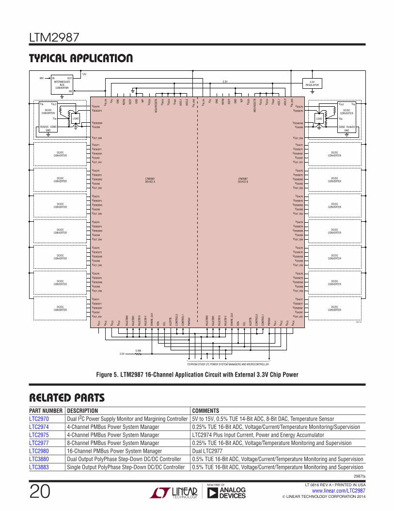
Figure 5. LTM2987 16-Channel Application Circuit with External 3.3V Chip Power
VINVOUT
RUN/SSSGND
VFB
GND
DC/DCCONVERTER
LOAD
VDACP0
VSENSEP0
VSENSEM0
VDACM0
VOUT_EN0
LTM2987DEVICE A
IN OUT
EN
INTERMEDIATEBUS
CONVERTER
V IN_
EN
3.3V
DNC
REFM
REFP
GND
WP
V DD2
5
V DD3
3
V DD3
3
V PW
R
ASEL
1
ASEL
0
V IN_
SNS
VDACP1
VSENSEP1
VSENSEM1
VDACM1
VOUT_EN1
DC/DCCONVERTER
VDACP2
VSENSEP2
VSENSEM2
VDACM2
VOUT_EN2
DC/DCCONVERTER
VDACP3
VSENSEP3
VSENSEM3
VDACM3
VOUT_EN3
DC/DCCONVERTER
VDACP4
VSENSEP4
VSENSEM4
VDACM4
VOUT_EN4
DC/DCCONVERTER
VDACP5
VSENSEP5
VSENSEM5
VDACM5
VOUT_EN5
DC/DCCONVERTER
VDACP6
VSENSEP6
VSENSEM6
VDACM6
VOUT_EN6
DC/DCCONVERTER
VDACP7
VSENSEP7
VSENSEM7
VDACM7
VOUT_EN7
DC/DCCONVERTER
2987 F05
VIN VOUT
RUN/SS SGND
VFB
GND
DC/DCCONVERTER
LOAD
VDACP0
VSENSEP0
VSENSEM0
VDACM0
VOUT_EN0
VDACP1
VSENSEP1
VSENSEM1
VDACM1
VOUT_EN1
DC/DCCONVERTER
VDACP7
VSENSEP7
VSENSEM7
VDACM7
VOUT_EN7
DC/DCCONVERTER
VDACP2
VSENSEP2
VSENSEM2
VDACM2
VOUT_EN2
DC/DCCONVERTER
VDACP6
VSENSEP6
VSENSEM6
VDACM6
VOUT_EN6
DC/DCCONVERTER
VDACP5
VSENSEP5
VSENSEM5
VDACM5
VOUT_EN5
DC/DCCONVERTER
VDACP4
VSENSEP4
VSENSEM4
VDACM4
VOUT_EN4
DC/DCCONVERTER
VDACP3
VSENSEP3
VSENSEM3
VDACM3
VOUT_EN3
DC/DCCONVERTER
DNC
REFM
REFP
GND
WP
V DD2
5
V DD3
3
V DD3
3
V PW
R
ASEL
1
ASEL
0
V IN_
SNS
LTM2987DEVICE B
V IN_
EN V PU
V PU
FAUL
TB00
FAUL
TB01
FAUL
TB10
FAUL
TB11
SHAR
E_CL
K
SDA
SCL
ALER
TB
CONT
ROL0
CONT
ROL1
PWRG
D
TO/FROM OTHER LTC POWER SYSTEM MANAGERS AND MICROCONTROLLER
FAUL
TB00
FAUL
TB01
FAUL
TB10
FAUL
TB11
SHAR
E_CL
K
SDA
SCL
ALER
TB
CONT
ROL0
CONT
ROL1
PWRG
D
R PU1
R PU2
R PU3
R PU4
R PU1
R PU2
R PU3
R PU4
3.3V5.49k
WDI
/RES
ETB
WDI
/RES
ETB
48V12V
3.3VREGULATOR