Embed Size (px)
Citation preview
LTC6820
16820fb
For more information www.linear.com/LTC6820
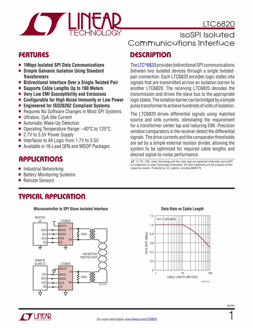
TYPICAL APPLICATION
FEATURES DESCRIPTION
isoSPI Isolated Communications Interface
The LTC®6820 provides bidirectional SPI communications between two isolated devices through a single twisted-pair connection. Each LTC6820 encodes logic states into signals that are transmitted across an isolation barrier to another LTC6820. The receiving LTC6820 decodes the transmission and drives the slave bus to the appropriate logic states. The isolation barrier can be bridged by a simple pulse transformer to achieve hundreds of volts of isolation.
The LTC6820 drives differential signals using matched source and sink currents, eliminating the requirement for a transformer center tap and reducing EMI. Precision window comparators in the receiver detect the differential signals. The drive currents and the comparator thresholds are set by a simple external resistor divider, allowing the system to be optimized for required cable lengths and desired signal-to-noise performance.
Microcontroller to SPI Slave Isolated Interface Data Rate vs Cable Length
APPLICATIONS
n 1Mbps Isolated SPI Data Communicationsn Simple Galvanic Isolation Using Standard
Transformersn Bidirectional Interface Over a Single Twisted Pairn Supports Cable Lengths Up to 100 Metersn Very Low EMI Susceptibility and Emissionsn Configurable for High Noise Immunity or Low Powern Engineered for ISO26262 Compliant Systemsn Requires No Software Changes in Most SPI Systemsn Ultralow, 2µA Idle Currentn Automatic Wake-Up Detectionn Operating Temperature Range: –40°C to 125°C n 2.7V to 5.5V Power Supplyn Interfaces to All Logic from 1.7V to 5.5Vn Available in 16-Lead QFN and MSOP Packages
n Industrial Networkingn Battery Monitoring Systemsn Remote Sensors
L, LT, LTC, LTM, Linear Technology and the Linear logo are registered trademarks and isoSPI is a trademark of Linear Technology Corporation. All other trademarks are the property of their respective owners. Protected by U.S. patents, including 8908779.
IP
120Ω
100 METERSTWISTED PAIR
LTC6820
MSTRMOSIMISOSCKCS
IM
MASTERµC
SDOSDISCK
CS
IP
120Ω
6820 TA01a
LTC6820
MSTR
MOSIMISOSCKCS
IM
REMOTESLAVE IC
SDISDOSCK
CS
CABLE LENGTH (METERS)1
0
DATA
RAT
E (M
bps)
0.2
0.4
0.6
0.8
1.2
10 100
6820 TA01b
1.0
CAT-5 ASSUMED
LTC6820
26820fb
For more information www.linear.com/LTC6820
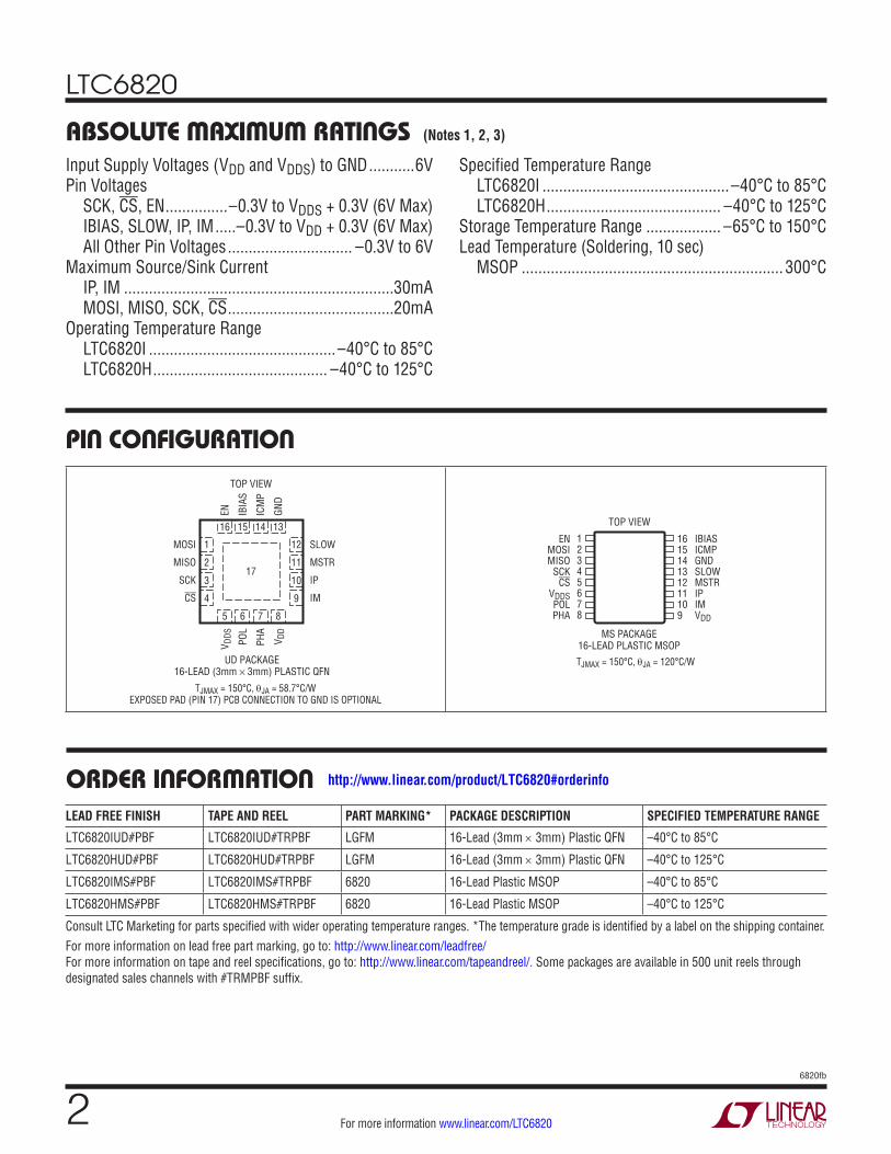
PIN CONFIGURATION
ABSOLUTE MAXIMUM RATINGSInput Supply Voltages (VDD and VDDS) to GND ...........6VPin Voltages SCK, CS, EN ...............–0.3V to VDDS + 0.3V (6V Max) IBIAS, SLOW, IP, IM .....–0.3V to VDD + 0.3V (6V Max) All Other Pin Voltages .............................. –0.3V to 6VMaximum Source/Sink Current IP, IM .................................................................30mA MOSI, MISO, SCK, CS ........................................20mAOperating Temperature Range LTC6820I .............................................–40°C to 85°C LTC6820H .......................................... –40°C to 125°C
(Notes 1, 2, 3)
16 15 14 13
5 6 7 8
TOP VIEW
17
UD PACKAGE16-LEAD (3mm × 3mm) PLASTIC QFN
9
10
11
12
4
3
2
1MOSI
MISO
SCK
CS
SLOW
MSTR
IP
IM
EN IBIA
S
ICM
P
GND
V DDS
POL
PHA
V DD
TJMAX = 150°C, θJA = 58.7°C/W
EXPOSED PAD (PIN 17) PCB CONNECTION TO GND IS OPTIONAL
12345678
ENMOSIMISO
SCKCS
VDDSPOLPHA
161514131211109
IBIASICMPGNDSLOWMSTRIPIMVDD
TOP VIEW
MS PACKAGE16-LEAD PLASTIC MSOP TJMAX = 150°C, θJA = 120°C/W
ORDER INFORMATIONLEAD FREE FINISH TAPE AND REEL PART MARKING* PACKAGE DESCRIPTION SPECIFIED TEMPERATURE RANGE
LTC6820IUD#PBF LTC6820IUD#TRPBF LGFM 16-Lead (3mm × 3mm) Plastic QFN –40°C to 85°C
LTC6820HUD#PBF LTC6820HUD#TRPBF LGFM 16-Lead (3mm × 3mm) Plastic QFN –40°C to 125°C
LTC6820IMS#PBF LTC6820IMS#TRPBF 6820 16-Lead Plastic MSOP –40°C to 85°C
LTC6820HMS#PBF LTC6820HMS#TRPBF 6820 16-Lead Plastic MSOP –40°C to 125°C
Consult LTC Marketing for parts specified with wider operating temperature ranges. *The temperature grade is identified by a label on the shipping container.For more information on lead free part marking, go to: http://www.linear.com/leadfree/ For more information on tape and reel specifications, go to: http://www.linear.com/tapeandreel/. Some packages are available in 500 unit reels through designated sales channels with #TRMPBF suffix.
Specified Temperature Range LTC6820I .............................................–40°C to 85°C LTC6820H .......................................... –40°C to 125°CStorage Temperature Range .................. –65°C to 150°CLead Temperature (Soldering, 10 sec) MSOP ............................................................... 300°C
http://www.linear.com/product/LTC6820#orderinfo
LTC6820
36820fb
For more information www.linear.com/LTC6820
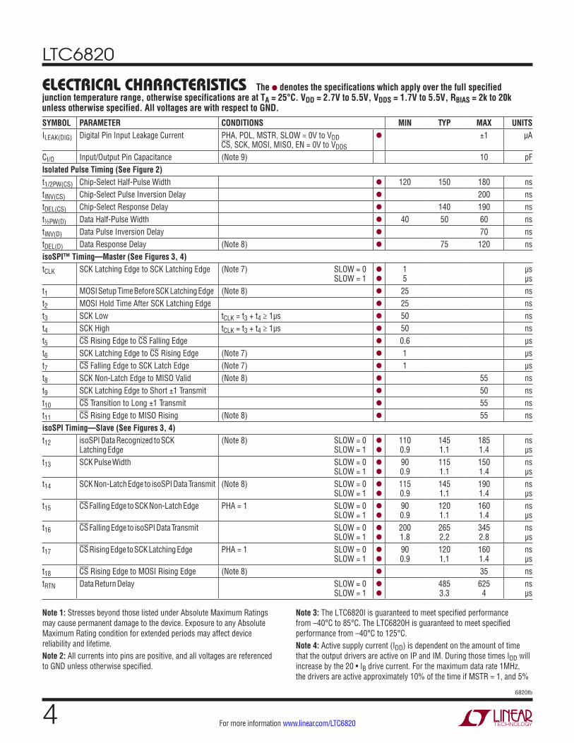
ELECTRICAL CHARACTERISTICS The l denotes the specifications which apply over the full specified temperature range, otherwise specifications are at TA = 25°C. VDD = 2.7V to 5.5V, VDDS = 1.7V to 5.5V, RBIAS = 2k to 20k unless otherwise specified. All voltages are with respect to GND.
SYMBOL PARAMETER CONDITIONS MIN TYP MAX UNITSPower SupplyVDD Operating Supply Voltage Range l 2.7 5.5 VVDDS IO Supply Voltage Range (Level Shifting) Affects CS, SCK, MOSI, MISO and EN Pins l 1.7 5.5 VIDD Supply Current, READY/ACTIVE States
(Note 4)RBIAS = 2kΩ (IB = 1mA) 1/tCLK = 0MHz 1/tCLK = 1MHz
l 4 4.8 7
5.8 mA mA
RBIAS = 20kΩ (IB = 0.1mA) 1/tCLK = 0MHz 1/tCLK = 1MHz
l 1.3 2 2.4
2.9 mA mA
Supply Current, IDLE State MSTR = 0V MSTR = VDD
l
l
2 1
6 3
µA µA
IDDS IO Supply Current (Note 5) SPI Inputs and EN Pin at 0V or VDDS, SPI Outputs Unloaded
l 1 µA
BiasingVBIAS Voltage on IBIAS Pin READY/ACTIVE State
IDLE Statel 1.9 2.0
02.1 V
VIB Isolated Interface Bias Current (Note 6) RBIAS = 2k to 20k l VBIAS/RBIAS mAAIB Isolated Interface Current Gain VA ≤ 1.6V IB = 1mA
IB = 0.1mAl
l
18 18
20 20
22 24
mA/mA mA/mA
VA Transmitter Pulse Amplitude VA = |VIP – VIM| VDD < 3.3V VDD ≥ 3.3V
l
l
VDD – 1.7V 1.6
V V
VICMP Threshold-Setting Voltage on ICMP Pin VTCMP = ATCMP • VICMP l 0.2 1.5 VILEAK(ICMP) Leakage Current on ICMP Pin VICMP = 0V to VDD l ±1 µAILEAK(IP/IM) Leakage Current on IP and IM Pins IDLE State, VIP = VIM = 0V to VDD l ±2 µAATCMP Receiver Comparator Threshold Voltage
GainVCM = VDD/2 to VDD – 0.2V, VICMP = 0.2V to 1.5V
l 0.4 0.5 0.6 V/V
VCM Receiver Common Mode Bias IP/IM Not Driving (VDD – VICMP/3 – 167mV) VRIN Receiver Input Resistance Single-Ended to IP or IM l 26 35 42 kΩIdle/Wake-Up (See Figures 13, 14, 15)VWAKE Differential Wake-Up Voltage
(See Figure 13)tDWELL = 240ns l 240 mV
tDWELL Dwell Time at VWAKE VWAKE = 240mV l 240 nstREADY Start-Up Time After Wake Detection l 8 µstIDLE Idle Time-Out Duration l 4 5.7 7.5 msDigital I/OVIH(CFG) Digital Voltage Input High, Configuration
Pins (PHA, POL, MSTR, SLOW)VDD = 2.7V to 5.5V (POL, PHA, MSTR, SLOW) l 0.7 • VDD V
VIL(CFG) Digital Voltage Input Low, Configuration Pins (PHA, POL, MSTR, SLOW)
VDD = 2.7V to 5.5V (POL, PHA, MSTR, SLOW) l 0.3 • VDD V
VIH(SPI) Digital Voltage Input High, SPI Pins (CS, SCK, MOSI, MISO)
VDDS = 2.7V to 5.5V VDDS = 1.7V to 2.7V
l
l
0.7 • VDDS 0.8 • VDDS
V V
VIL(SPI) Digital Voltage Input Low, SPI Pins (CS, SCK, MOSI, MISO)
VDDS = 2.7V to 5.5V VDDS = 1.7V to 2.7V
l
l
0.3 • VDDS 0.2 • VDDS
V V
VIH(EN) Digital Voltage Input High, EN Pin VDDS = 2.7V to 5.5V VDDS = 1.7V to 2.7V
l
l
2 0.85 • VDDS
V V
VIL(EN) Digital Voltage Input Low, EN Pin VDDS = 2.7V to 5.5V VDDS = 1.7V to 2.7V
l
l
0.8 0.25 • VDDS
V V
VOH Digital Voltage Output High (CS and SCK) VDDS = 3.3V, Sourcing 2mA VDDS = 1.7V, Sourcing 1mA
l
l
VDDS – 0.2 VDDS – 0.25
V V
VOL Digital Voltage Output Low (MOSI, MISO, CS, SCK)
VDDS = 3.3V, Sinking 3.3mA VDDS = 1.7V, Sinking 1mA
l
l
0.2 0.2
V V
LTC6820
46820fb
For more information www.linear.com/LTC6820
ELECTRICAL CHARACTERISTICS The l denotes the specifications which apply over the full specified junction temperature range, otherwise specifications are at TA = 25°C. VDD = 2.7V to 5.5V, VDDS = 1.7V to 5.5V, RBIAS = 2k to 20k unless otherwise specified. All voltages are with respect to GND.
SYMBOL PARAMETER CONDITIONS MIN TYP MAX UNITSILEAK(DIG) Digital Pin Input Leakage Current PHA, POL, MSTR, SLOW = 0V to VDD
CS, SCK, MOSI, MISO, EN = 0V to VDDS
l ±1 µA
CI/O Input/Output Pin Capacitance (Note 9) 10 pFIsolated Pulse Timing (See Figure 2)t1/2PW(CS) Chip-Select Half-Pulse Width l 120 150 180 nstINV(CS) Chip-Select Pulse Inversion Delay l 200 nstDEL(CS) Chip-Select Response Delay l 140 190 nst½PW(D) Data Half-Pulse Width l 40 50 60 nstINV(D) Data Pulse Inversion Delay l 70 nstDEL(D) Data Response Delay (Note 8) l 75 120 nsisoSPI™ Timing—Master (See Figures 3, 4)tCLK SCK Latching Edge to SCK Latching Edge (Note 7) SLOW = 0
SLOW = 1l
l
1 5
µs µs
t1 MOSI Setup Time Before SCK Latching Edge (Note 8) l 25 nst2 MOSI Hold Time After SCK Latching Edge l 25 nst3 SCK Low tCLK = t3 + t4 ≥ 1µs l 50 nst4 SCK High tCLK = t3 + t4 ≥ 1µs l 50 nst5 CS Rising Edge to CS Falling Edge l 0.6 µst6 SCK Latching Edge to CS Rising Edge (Note 7) l 1 µst7 CS Falling Edge to SCK Latch Edge (Note 7) l 1 µst8 SCK Non-Latch Edge to MISO Valid (Note 8) l 55 nst9 SCK Latching Edge to Short ±1 Transmit l 50 nst10 CS Transition to Long ±1 Transmit l 55 nst11 CS Rising Edge to MISO Rising (Note 8) l 55 nsisoSPI Timing—Slave (See Figures 3, 4)t12 isoSPI Data Recognized to SCK
Latching Edge(Note 8) SLOW = 0 SLOW = 1
l
l
110 0.9
145 1.1
185 1.4
ns µs
t13 SCK Pulse Width SLOW = 0 SLOW = 1
l
l
90 0.9
115 1.1
150 1.4
ns µs
t14 SCK Non-Latch Edge to isoSPI Data Transmit (Note 8) SLOW = 0 SLOW = 1
l
l
115 0.9
145 1.1
190 1.4
ns µs
t15 CS Falling Edge to SCK Non-Latch Edge PHA = 1 SLOW = 0 SLOW = 1
l
l
90 0.9
120 1.1
160 1.4
ns µs
t16 CS Falling Edge to isoSPI Data Transmit SLOW = 0 SLOW = 1
l
l
200 1.8
265 2.2
345 2.8
ns µs
t17 CS Rising Edge to SCK Latching Edge PHA = 1 SLOW = 0 SLOW = 1
l
l
90 0.9
120 1.1
160 1.4
ns µs
t18 CS Rising Edge to MOSI Rising Edge (Note 8) l 35 nstRTN Data Return Delay SLOW = 0
SLOW = 1l
l
485 3.3
625 4
ns µs
Note 1: Stresses beyond those listed under Absolute Maximum Ratings may cause permanent damage to the device. Exposure to any Absolute Maximum Rating condition for extended periods may affect device reliability and lifetime.Note 2: All currents into pins are positive, and all voltages are referenced to GND unless otherwise specified.
Note 3: The LTC6820I is guaranteed to meet specified performance from –40°C to 85°C. The LTC6820H is guaranteed to meet specified performance from –40°C to 125°C.Note 4: Active supply current (IDD) is dependent on the amount of time that the output drivers are active on IP and IM. During those times IDD will increase by the 20 • IB drive current. For the maximum data rate 1MHz, the drivers are active approximately 10% of the time if MSTR = 1, and 5%
LTC6820
56820fb
For more information www.linear.com/LTC6820
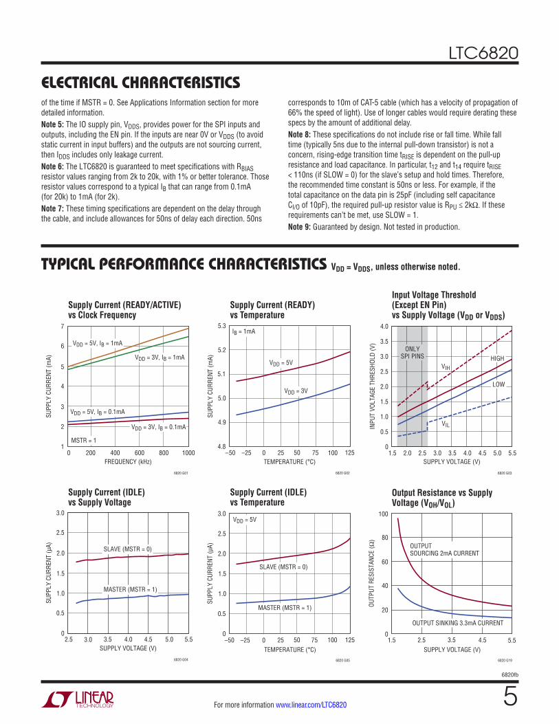
TYPICAL PERFORMANCE CHARACTERISTICS
Supply Current (IDLE)vs Supply Voltage
Supply Current (IDLE)vs Temperature
Supply Current (READY/ACTIVE)vs Clock Frequency
Supply Current (READY)vs Temperature
Input Voltage Threshold (Except EN Pin) vs Supply Voltage (VDD or VDDS)
ELECTRICAL CHARACTERISTICSof the time if MSTR = 0. See Applications Information section for more detailed information. Note 5: The IO supply pin, VDDS, provides power for the SPI inputs and outputs, including the EN pin. If the inputs are near 0V or VDDS (to avoid static current in input buffers) and the outputs are not sourcing current, then IDDS includes only leakage current.Note 6: The LTC6820 is guaranteed to meet specifications with RBIAS resistor values ranging from 2k to 20k, with 1% or better tolerance. Those resistor values correspond to a typical IB that can range from 0.1mA (for 20k) to 1mA (for 2k). Note 7: These timing specifications are dependent on the delay through the cable, and include allowances for 50ns of delay each direction. 50ns
corresponds to 10m of CAT-5 cable (which has a velocity of propagation of 66% the speed of light). Use of longer cables would require derating these specs by the amount of additional delay.Note 8: These specifications do not include rise or fall time. While fall time (typically 5ns due to the internal pull-down transistor) is not a concern, rising-edge transition time tRISE is dependent on the pull-up resistance and load capacitance. In particular, t12 and t14 require tRISE < 110ns (if SLOW = 0) for the slave’s setup and hold times. Therefore, the recommended time constant is 50ns or less. For example, if the total capacitance on the data pin is 25pF (including self capacitance CI/O of 10pF), the required pull-up resistor value is RPU ≤ 2kΩ. If these requirements can’t be met, use SLOW = 1.Note 9: Guaranteed by design. Not tested in production.
VDD = VDDS, unless otherwise noted.
FREQUENCY (kHz)0
1
SUPP
LY C
URRE
NT (m
A)
2
3
4
5
6
7
200 400 600 800
6820 G01
1000
VDD = 5V, IB = 1mA
VDD = 5V, IB = 0.1mA
VDD = 3V, IB = 1mA
VDD = 3V, IB = 0.1mA
MSTR = 1
TEMPERATURE (°C)–50 –25
4.8
SUPP
LY C
URRE
NT (m
A)
5.0
5.3
0 50 75
6820 G02
4.9
5.2
5.1
25 100 125
VDD = 5V
VDD = 3V
IB = 1mA
SUPPLY VOLTAGE (V)1.5 2.5
0
INPU
T VO
LTAG
E TH
RESH
OLD
(V)
0.5
1.0
1.5
2.0
4.0
VIH
VIL
3.02.0 3.5 4.0 4.5
6820 G03
5.0 5.5
3.5
3.0
2.5
ONLYSPI PINS HIGH
LOW
SUPPLY VOLTAGE (V)2.5
0
SUPP
LY C
URRE
NT (µ
A)
0.5
1.0
1.5
2.0
3.0
3.0 3.5 4.0 4.5
6820 G04
5.0 5.5
2.5
SLAVE (MSTR = 0)
MASTER (MSTR = 1)
TEMPERATURE (°C)–50
SUPP
LY C
URRE
NT (µ
A)
3.0
25 75
6820 G05
2.0
–25 0 50 100 125
1.0
0
2.5
1.5
0.5
VDD = 5V
SLAVE (MSTR = 0)
MASTER (MSTR = 1)
Output Resistance vs Supply Voltage (VOH/VOL)
SUPPLY VOLTAGE (V)1.5
OUTP
UT R
ESIS
TANC
E (Ω
)
40
60
5.5
6820 G19
20
02.5 3.5 4.5
100
80OUTPUT SOURCING 2mA CURRENT
OUTPUT SINKING 3.3mA CURRENT
LTC6820
66820fb
For more information www.linear.com/LTC6820
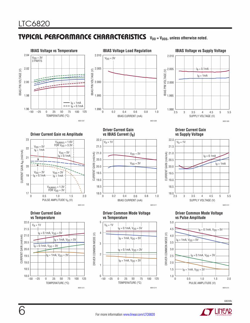
TYPICAL PERFORMANCE CHARACTERISTICS
Driver Current Gain vs AmplitudeDriver Current Gain vs IBIAS Current (IB)
Driver Current Gain vs Supply Voltage
Driver Current Gain vs Temperature
Driver Common Mode Voltage vs Temperature
Driver Common Mode Voltage vs Pulse Amplitude
IBIAS Voltage vs Temperature IBIAS Voltage Load Regulation IBIAS Voltage vs Supply Voltage
VDD = VDDS, unless otherwise noted.
IBIAS CURRENT (mA)0
IBIA
S PI
N VO
LTAG
E (V
)
2.000
2.005
0.8
6820 G08
1.995
1.9900.2 0.4 0.6 1.0
2.010VDD = 3V
SUPPLY VOLTAGE (V)2.5
1.990
IBIA
S PI
N VO
LTAG
E (V
)
1.995
2.000
2.005
2.010
3 3.5 4 4.5
6820 G09
5 5.5
IB = 0.1mA
IB = 1mA
PULSE AMPLITUDE VA (V)0
17
CURR
ENT
GAIN
AIB
(mA/
mA)
18
19
20
21
22
23
0.5 1.0 1.5
6820 G10
2.0
VDD = 3VIB = 1mA
VDD = 5VIB = 1mA
VDD = 5VIB = 0.1mA
VDD = 3VIB = 0.1mA
VA(MAX) = 1.6VFOR VDD > 3.3V
VA(MAX) = 1.3VFOR VDD = 3V
IBIAS CURRENT (mA)0
CURR
ENT
GAIN
(mA/
mA)
19.5
20.0
20.5
0.6 1.0
VA = 1V
6820 G11
19.0
18.5
18.00.2 0.4 0.8
21.0
21.5
22.0
VDD = 5V
VDD = 3V
SUPPLY VOLTAGE (V)2.5
CURR
ENT
GAIN
(mA/
mA)20.0
6820 G12
19.0
18.03.5 4.53 4 5
21.0
22.0
19.5
18.5
20.5
21.5
VA = 1V
IB = 0.1mA
IB = 1mA
5.5
TEMPERATURE (°C)–50
CURR
ENT
GAIN
(mA/
mA)
21.5
25
6820 G13
20.0
19.0
–25 0 50
18.5
18.0
22.0
21.0
20.5
19.5
75 100 125
IB = 0.1mA, VDD = 5V
VA = 1V
IB = 0.1mA, VDD = 3V
IB = 1mA, VDD = 5V
IB = 1mA, VDD = 3V
TEMPERATURE (°C)–50 –25
0
DRIV
ER C
OMM
ON M
ODE
(V)
2
5
0 50 75
6820 G14
1
4
3
25 100 125
IB = 0.1mA, VDD = 5V
IB = 0.1mA, VDD = 3V
IB = 1mA, VDD = 5V
IB = 1mA, VDD = 3V
VA = 1V
PULSE AMPLITUDE (V)0
DRIV
ER C
OMM
ON M
ODE
(V)
3.0
4.0
5.0
6820 G15
2.0
2.5
3.5
4.5
1.5
1.00.5 1.0 1.5 2.0
IB = 0.1mA, VDD = 5V
IB = 0.1mA, VDD = 3V
IB = 1mA, VDD = 5V
IB = 1mA, VDD = 3V
TEMPERATURE (°C)–50 –25
1.96
IBIA
S PI
N VO
LTAG
E (V
)
1.98
2.04
0 50 75
6820 G07
2.02
2.00
25 100 125
VDD = 3V3 PARTS
IB = 1mAIB = 0.1mA
LTC6820
76820fb
For more information www.linear.com/LTC6820
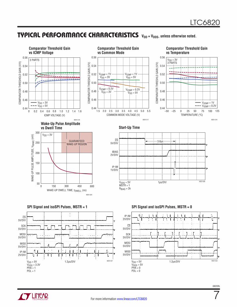
TYPICAL PERFORMANCE CHARACTERISTICS VDD = VDDS, unless otherwise noted.
Wake-Up Pulse Amplitude vs Dwell Time
Comparator Threshold Gainvs ICMP Voltage
Comparator Threshold Gainvs Common Mode
Comparator Threshold Gainvs Temperature
SPI Signal and isoSPI Pulses, MSTR = 1 SPI Signal and isoSPI Pulses, MSTR = 0
Start-Up Time
CS5V/DIV
SCK5V/DIV
MOSI5V/DIV
MIS05V/DIV
IP-IM2V/DIV
1.2µs/DIV 6820 G21VDD = 5VVDDS = 3.3VPHA = 1POL = 1
CS5V/DIV
SCK5V/DIV
MOSI5V/DIV
MIS05V/DIV
IP-IM2V/DIV
1.2µs/DIV 6820 G22VDD = 5VVDDS = 5VPHA = 0POL = 0
CS5V/DIV
IBIAS2V/DIV
IP-IM1V/DIV
1µs/DIV 6820 G06VDDS = 5VMSTR = 1RBIAS = 2k
3.6µs
ICMP VOLTAGE (V)0
COM
PARA
TOR
THRE
SHOL
D GA
IN (V
/V)
0.52
0.50
0.54
0.56
0.6 1.0 1.6
6820 G16
0.48
0.46
0.440.2 0.4 0.8 1.2 1.4
3 PARTS
VDD = 3VVDD = 5V
COMMON MODE VOLTAGE (V)1.5 2.0
COM
PARA
TOR
THRE
SHLD
GAI
N (V
/V)
2.5 3.5 4.0
6820 G17
3.0 4.5 5.55.0
VICMP = 1VVDD = 3V
VICMP = 0.2VVDD = 5V
VICMP = 0.2VVDD = 3V
VICMP = 1VVDD = 5V
0.52
0.50
0.54
0.56
0.48
0.46
0.44
TEMPERATURE (°C)–50 –25
COM
PARA
TOR
THRE
SHLD
GAI
N (V
/V)
0 50 75
6820 G18
25 100 125
VDD = 3V3 PARTS
VICMP = 1VVICMP = 0.2V
0.52
0.50
0.54
0.56
0.48
0.46
0.44
WAKE-UP DWELL TIME, tDWELL (ns)0
WAK
E-UP
PUL
SE A
MPL
ITUD
E, V
WAK
E (m
V)
150
200
600
6820 G20
100
50150 300 450
300
250 GUARANTEEDWAKE-UP REGION
VDD = 3V
LTC6820
86820fb
For more information www.linear.com/LTC6820
PIN FUNCTIONS (QFN/MSOP)
MOSI (Pin 1/Pin 2): SPI Master Out/Slave In Data. If connected on the master side of a SPI interface (MSTR pin high), this pin receives the data signal output from the master SPI controller. If connected on the slave side of the interface (MSTR pin low), this pin drives the data signal input to the slave SPI device. The output is open drain, so an external pull-up resistor to VDDS is required.
MISO (Pin 2/Pin 3): SPI Master In/Slave Out Data. If con-nected on the master side of a SPI interface (MSTR pin high), this pin drives the data signal input to the master SPI controller. If connected on the slave side of the interface (MSTR pin low), this pin receives the data signal output from the slave SPI device. The output is open drain, so an external pull-up resistor to VDDS is required.
SCK (Pin 3/Pin 4): SPI Clock Input/Output. If connected on the master side of the interface (MSTR pin high), this pin receives the clock signal from the master SPI controller. This input should not be pulled above VDDS. If connected on the slave side of the interface (MSTR pin low), this pin outputs the clock signal to the slave device. The output driver is push-pull; no external pull-up resistor is needed.
CS (Pin 4/Pin 5): SPI Chip Select Input/Output. If connected on the master side of the interface (MSTR pin high), this pin receives the chip select signal from the master SPI controller. This input should not be pulled above VDDS. If connected on the slave side of the interface (MSTR pin low), this pin outputs the chip select signal to the slave device. The output driver is push-pull; no external pull-up resistor is needed.
VDDS (Pin 5/Pin 6): SPI Input/Output Power Supply Input. The output drivers for the SCK and CS pins use the VDDS input as their positive power supply. The input threshold voltages of SCK, CS, MOSI, MISO and EN are determined by VDDS. May be tied to VDD or to a supply above or below VDD to level shift the SPI I/O. If separate from VDD, con-nect a bypass capacitor of at least 0.01μF directly between VDDS and GND.
POL (Pin 6/Pin 7): SPI Clock Polarity Input. Tie to VDD or GND. See Operation section for details.
PHA (Pin 7/Pin 8): SPI Clock Phase Input. Tie to VDD or GND. See Operation section for details.
VDD (Pin 8/Pin 9): Device Power Supply Input. Connect a bypass capacitor of at least 0.01μF directly between VDD and GND.
IM (Pin 9/Pin 10): Isolated Interface Minus Input/Output.
IP (Pin 10/Pin 11): Isolated Interface Plus Input/Output.
MSTR (Pin 11/Pin 12): Serial Interface Master/Slave Selector Input. Tie this pin to VDD if the device is on the master side of the isolated interface. Tie this pin to GND if the device is on the slave side of the isolated interface.
SLOW (Pin 12/Pin 13): Slow Interface Selection Input. For clock frequencies at or below 200kHz, or if slave devices cannot meet timing requirements, this pin should be tied to VDD. For clock frequencies above 200kHz, this pin should be tied to GND.
GND (Pin 13/Pin 14): Device Ground.
ICMP (Pin 14/Pin 15): Isolated Interface Comparator Voltage Threshold Set. Tie this pin to the resistor divider between IBIAS and GND to set the voltage threshold of the interface receiver comparators. The comparator thresholds are set to 1/2 the voltage on the ICMP pin.
IBIAS (Pin 15/Pin 16): Isolated Interface Current Bias. Tie IBIAS to GND through a resistor divider to set the interface output current level. When the device is enabled, this pin is approximately 2V. When transmitting pulses, the sink current on each of the IP and IM pins is set to 20 times the current sourced from pin IBIAS to GND. Limit the capacitance on the IBIAS pin to less than 50pF to maintain the stability of the feedback circuit regulating the IBIAS voltage.
EN (Pin 16/Pin 1): Device Enable Input. If high, this pin forces the LTC6820 to stay enabled, overriding the internal IDLE mode function. If low, the LTC6820 will go into IDLE mode after the CS pin has been high for 5.7ms (when MSTR pin is high) or after no signal on the IP/IM pins for 5.7ms (when MSTR pin is low). The LTC6820 will wake-up less than 8µs after CS falls (MSTR high) or after a signal is detected on IP/IM (MSTR low).
Exposed Pad (Pin 17, QFN Package Only): Exposed pad may be left open or connected to device GND.
LTC6820
96820fb
For more information www.linear.com/LTC6820
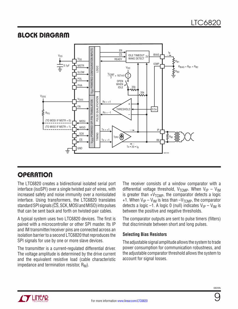
BLOCK DIAGRAM
OPERATION
+–
IDRV
IP
IBIASIB
ICMP
IMRM
6820 BD
RPU
RB1
RB2
Tx = –1CS
Tx • 20 • IB
Tx = +1
Rx = +1
Rx = –1 –
+THRESHOLD 0.5x
35k
35k
VDD
READY
RBIAS = RB1 + RB2
OPENWHEN
IDLE
+ 167mVVICMP
3
IDLE TIMEOUTWAKE DETECT
CS
EN
2V
SCK
GND
MISO
MOSI
EN
VDDS
VDDS
VDD
PHA
POL
SLOW
MSTR
V DD-
POW
ERED
CON
FIGU
RATI
ON IN
PUTS
V DDS
-POW
ERED
SPI
PIN
TRA
NSLA
TION
TIM
ING
PULS
E QU
ALIF
ICAT
ION
LOGI
C
VDD
0.1µF
(TO MISO IF MSTR = 1)
(TO MOSI IF MSTR = 0)
The LTC6820 creates a bidirectional isolated serial port interface (isoSPI) over a single twisted pair of wires, with increased safety and noise immunity over a nonisolated interface. Using transformers, the LTC6820 translates standard SPI signals (CS, SCK, MOSI and MISO) into pulses that can be sent back and forth on twisted-pair cables.
A typical system uses two LTC6820 devices. The first is paired with a microcontroller or other SPI master. Its IP and IM transmitter/receiver pins are connected across an isolation barrier to a second LTC6820 that reproduces the SPI signals for use by one or more slave devices.
The transmitter is a current-regulated differential driver. The voltage amplitude is determined by the drive current and the equivalent resistive load (cable characteristic impedance and termination resistor, RM).
The receiver consists of a window comparator with a differential voltage threshold, VTCMP. When VIP – VIM is greater than +VTCMP, the comparator detects a logic +1. When VIP – VIM is less than –VTCMP, the comparator detects a logic –1. A logic 0 (null) indicates VIP – VIM is between the positive and negative thresholds.
The comparator outputs are sent to pulse timers (filters) that discriminate between short and long pulses.
Selecting Bias Resistors
The adjustable signal amplitude allows the system to trade power consumption for communication robustness, and the adjustable comparator threshold allows the system to account for signal losses.
LTC6820
106820fb
For more information www.linear.com/LTC6820
OPERATION
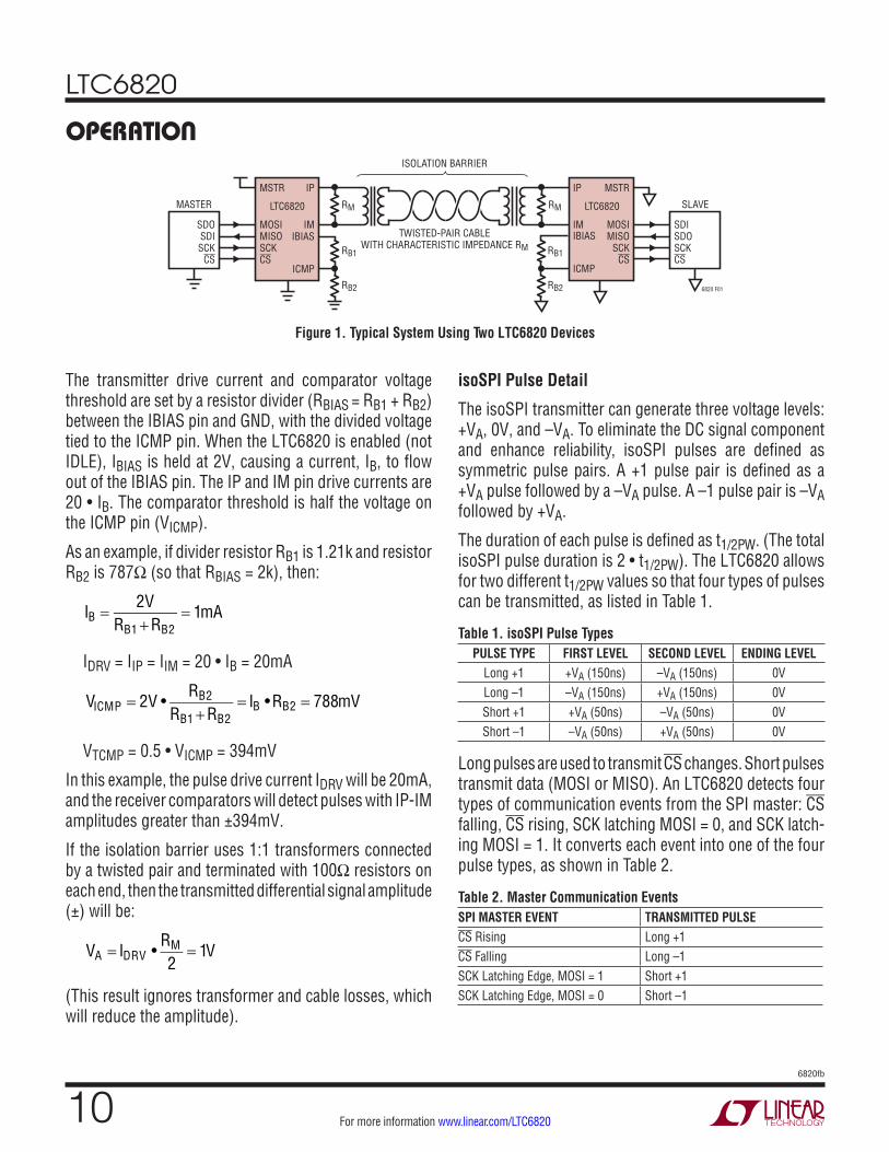
Figure 1. Typical System Using Two LTC6820 Devices
RM
IP MSTR
IMIBIAS
ICMP
6820 F01
MOSIMISO
SCKCS
SDISDOSCKCS
LTC6820 SLAVERM
RB1
RB2
RB1
RB2
IPMSTR
IMIBIAS
ICMP
MOSIMISOSCKCS
SDOSDISCK
CS
LTC6820
TWISTED-PAIR CABLEWITH CHARACTERISTIC IMPEDANCE RM
ISOLATION BARRIER
MASTER
The transmitter drive current and comparator voltage threshold are set by a resistor divider (RBIAS = RB1 + RB2) between the IBIAS pin and GND, with the divided voltage tied to the ICMP pin. When the LTC6820 is enabled (not IDLE), IBIAS is held at 2V, causing a current, IB, to flow out of the IBIAS pin. The IP and IM pin drive currents are 20 • IB. The comparator threshold is half the voltage on the ICMP pin (VICMP).
As an example, if divider resistor RB1 is 1.21k and resistor RB2 is 787Ω (so that RBIAS = 2k), then:
IB =
2VRB1 +RB2
= 1mA
IDRV = IIP = IIM = 20 • IB = 20mA
VICMP = 2V •
RB2
RB1 +RB2= IB •RB2 = 788mV
VTCMP = 0.5 • VICMP = 394mV
In this example, the pulse drive current IDRV will be 20mA, and the receiver comparators will detect pulses with IP-IM amplitudes greater than ±394mV.
If the isolation barrier uses 1:1 transformers connected by a twisted pair and terminated with 100Ω resistors on each end, then the transmitted differential signal amplitude (±) will be:
VA = IDRV •
RM
2= 1V
(This result ignores transformer and cable losses, which will reduce the amplitude).
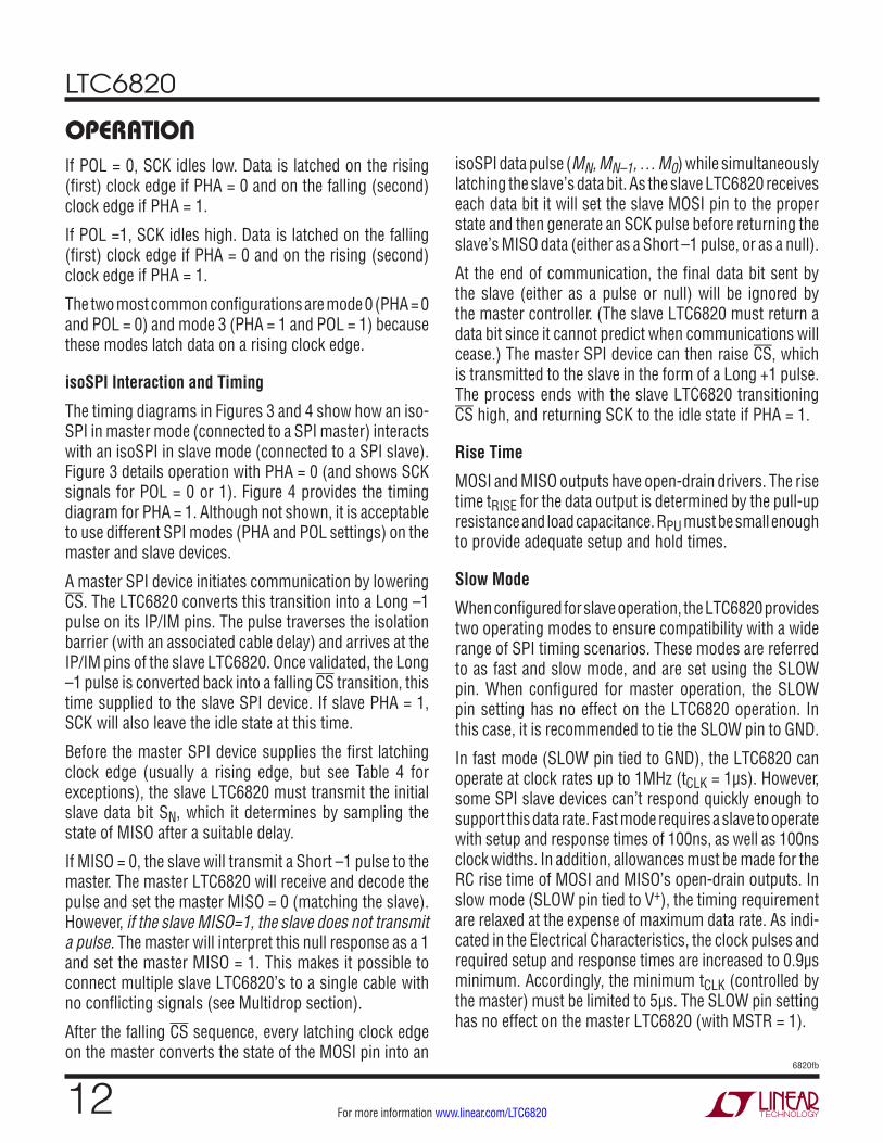
isoSPI Pulse Detail
The isoSPI transmitter can generate three voltage levels: +VA, 0V, and –VA. To eliminate the DC signal component and enhance reliability, isoSPI pulses are defined as symmetric pulse pairs. A +1 pulse pair is defined as a +VA pulse followed by a –VA pulse. A –1 pulse pair is –VA followed by +VA.
The duration of each pulse is defined as t1/2PW. (The total isoSPI pulse duration is 2 • t1/2PW). The LTC6820 allows for two different t1/2PW values so that four types of pulses can be transmitted, as listed in Table 1.
Table 1. isoSPI Pulse TypesPULSE TYPE FIRST LEVEL SECOND LEVEL ENDING LEVEL
Long +1 +VA (150ns) –VA (150ns) 0VLong –1 –VA (150ns) +VA (150ns) 0VShort +1 +VA (50ns) –VA (50ns) 0VShort –1 –VA (50ns) +VA (50ns) 0V
Long pulses are used to transmit CS changes. Short pulses transmit data (MOSI or MISO). An LTC6820 detects four types of communication events from the SPI master: CS falling, CS rising, SCK latching MOSI = 0, and SCK latch-ing MOSI = 1. It converts each event into one of the four pulse types, as shown in Table 2.
Table 2. Master Communication EventsSPI MASTER EVENT TRANSMITTED PULSECS Rising Long +1CS Falling Long –1SCK Latching Edge, MOSI = 1 Short +1SCK Latching Edge, MOSI = 0 Short –1
LTC6820
116820fb
For more information www.linear.com/LTC6820
OPERATIONOn the other side of the isolation barrier (i.e., the other end of the cable) another LTC6820 is configured to interface with a SPI slave. It receives the transmitted pulses and reconstructs the SPI signals on its output port, as shown in Table 3. In addition, the slave device may transmit a return data pulse to the master to set the state of MISO. See isoSPI Interaction and Timing for additional details.
Table 3. Slave SPI Port OutputRECEIVED PULSE SPI PORT ACTION RETURN PULSE
Long +1 Drive CS High None
Long –1 Drive CS LowShort –1 Pulse if MISO = 0(No Return Pulse if MISO = 1)
Short +1 1. Set MOSI = 1 2. Pulse SCK
Short –1 1. Set MOSI = 0 2. Pulse SCK
A slave LTC6820 never transmits long (CS) pulses. Fur-thermore, a slave will only transmit a short –1 pulse (when MISO = 0), never a +1 pulse. This allows for multiple slave devices on a single cable without risk of collisions (see Multidrop section).
isoSPI Pulse Specifications
Figure 2 details the timing specifications for the +1 and –1 isoSPI pulses. The same timing specifications apply to either version of these symmetric pulses. In the Electrical
VA+1 PULSE
–1 PULSE
–VA
MOSI, MISO OR CS
VTCMPt1/2PW
t1/2PW–VTCMP
VIP – VIM
VA
–VA
MOSI, MISO OR CS
VTCMP
–VTCMP
VIP – VIMt1/2PW
t1/2PW
tINV
tINV
tDEL
tDEL
6820 F02
Characteristics table, these specifications are further separated into CS (long) and Data (short) parameters.
A valid pulse must meet the minimum spec for t1/2PW and the maximum spec for tINV. In other words, the half-pulse width must be long enough to pass through the appropriate pulse timer, but short enough for the inversion to begin within the valid window of time.
The response observed at MOSI, MISO or CS will occur after delay tDEL from the pulse inversion.
Setting Clock Phase and Polarity (PHA and POL)
SPI devices often use one clock edge to latch data and the other edge to shift data. This avoids timing problems associated with clock skew. There is no standard to specify whether the shift or latch occurs first. There is also no requirement for data to be latched on a rising or falling clock edge, although latching on the rising edge is most common. The LTC6820 supports all four SPI operating modes, as configured by the PHA and POL Pins.
Table 4. SPI ModesMODE POL PHA DESCRIPTION
0 0 0 SCK Idles Low, Latches on Rising (1st) Edge
1 0 1 SCK Idles Low, Latches on Falling (2nd) Edge
2 1 0 SCK Idles High, Latches on Falling (1st) Edge
3 1 1 SCK Idles High, Latches on Rising (2nd) Edge
Figure 2. isoSPI Differential Pulse Detail
LTC6820
126820fb
For more information www.linear.com/LTC6820
OPERATIONIf POL = 0, SCK idles low. Data is latched on the rising (first) clock edge if PHA = 0 and on the falling (second) clock edge if PHA = 1.
If POL =1, SCK idles high. Data is latched on the falling (first) clock edge if PHA = 0 and on the rising (second) clock edge if PHA = 1.
The two most common configurations are mode 0 (PHA = 0 and POL = 0) and mode 3 (PHA = 1 and POL = 1) because these modes latch data on a rising clock edge.
isoSPI Interaction and Timing
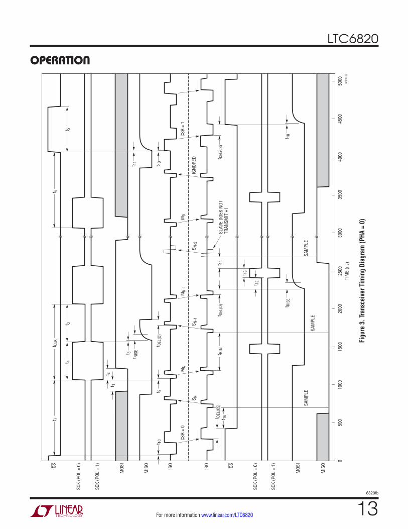
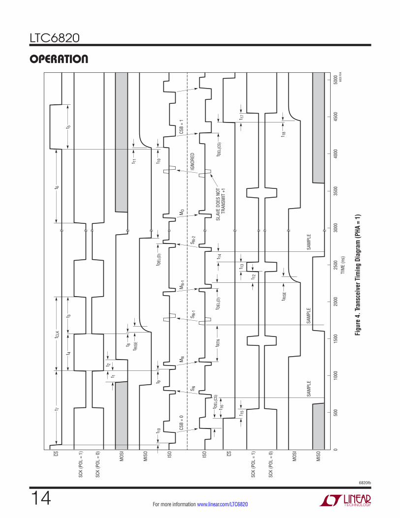
The timing diagrams in Figures 3 and 4 show how an iso-SPI in master mode (connected to a SPI master) interacts with an isoSPI in slave mode (connected to a SPI slave). Figure 3 details operation with PHA = 0 (and shows SCK signals for POL = 0 or 1). Figure 4 provides the timing diagram for PHA = 1. Although not shown, it is acceptable to use different SPI modes (PHA and POL settings) on the master and slave devices.
A master SPI device initiates communication by lowering CS. The LTC6820 converts this transition into a Long –1 pulse on its IP/IM pins. The pulse traverses the isolation barrier (with an associated cable delay) and arrives at the IP/IM pins of the slave LTC6820. Once validated, the Long –1 pulse is converted back into a falling CS transition, this time supplied to the slave SPI device. If slave PHA = 1, SCK will also leave the idle state at this time.
Before the master SPI device supplies the first latching clock edge (usually a rising edge, but see Table 4 for exceptions), the slave LTC6820 must transmit the initial slave data bit SN, which it determines by sampling the state of MISO after a suitable delay.
If MISO = 0, the slave will transmit a Short –1 pulse to the master. The master LTC6820 will receive and decode the pulse and set the master MISO = 0 (matching the slave). However, if the slave MISO=1, the slave does not transmit a pulse. The master will interpret this null response as a 1 and set the master MISO = 1. This makes it possible to connect multiple slave LTC6820’s to a single cable with no conflicting signals (see Multidrop section).
After the falling CS sequence, every latching clock edge on the master converts the state of the MOSI pin into an
isoSPI data pulse (MN, MN–1, … M0) while simultaneously latching the slave’s data bit. As the slave LTC6820 receives each data bit it will set the slave MOSI pin to the proper state and then generate an SCK pulse before returning the slave’s MISO data (either as a Short –1 pulse, or as a null).
At the end of communication, the final data bit sent by the slave (either as a pulse or null) will be ignored by the master controller. (The slave LTC6820 must return a data bit since it cannot predict when communications will cease.) The master SPI device can then raise CS, which is transmitted to the slave in the form of a Long +1 pulse. The process ends with the slave LTC6820 transitioning CS high, and returning SCK to the idle state if PHA = 1.
Rise Time
MOSI and MISO outputs have open-drain drivers. The rise time tRISE for the data output is determined by the pull-up resistance and load capacitance. RPU must be small enough to provide adequate setup and hold times.
Slow Mode
When configured for slave operation, the LTC6820 provides two operating modes to ensure compatibility with a wide range of SPI timing scenarios. These modes are referred to as fast and slow mode, and are set using the SLOW pin. When configured for master operation, the SLOW pin setting has no effect on the LTC6820 operation. In this case, it is recommended to tie the SLOW pin to GND.
In fast mode (SLOW pin tied to GND), the LTC6820 can operate at clock rates up to 1MHz (tCLK = 1µs). However, some SPI slave devices can’t respond quickly enough to support this data rate. Fast mode requires a slave to operate with setup and response times of 100ns, as well as 100ns clock widths. In addition, allowances must be made for the RC rise time of MOSI and MISO’s open-drain outputs. In slow mode (SLOW pin tied to V+), the timing requirement are relaxed at the expense of maximum data rate. As indi-cated in the Electrical Characteristics, the clock pulses and required setup and response times are increased to 0.9µs minimum. Accordingly, the minimum tCLK (controlled by the master) must be limited to 5µs. The SLOW pin setting has no effect on the master LTC6820 (with MSTR = 1).
LTC6820
136820fb
For more information www.linear.com/LTC6820
OPERATION
SCK
(POL
= 0
)
ISO
ISO
MIS
O
MOS
I
SCK
(POL
= 1
)
SCK
(POL
= 0
)
t 7
t 4
t 1
CS CS
SCK
(POL
= 1
)
MOS
I
MIS
O
500
010
0015
0020
0025
00TI
ME
(ns)
3000
SAM
PLE
SAM
PLE
3500
4000
4500
5000
6820
F03
t CLK
t 6
t 3t 5
t 2
t 8t 1
1
t 10
t 9t D
EL(D
)
t RIS
E
t RIS
E
t 10
t 16
t 14
t 13
t 18
t DEL
(CS)
SAM
PLE
t RTN
t DEL
(CS)
CSB
= 0
MN
MN-
1M
0CS
B =
1
S NS N
-1S N
-2IG
NORE
D
SLAV
E DO
ES N
OTTR
ANSM
IT +
1
t 12
t DEL
(D)
Figu
re 3
. Tra
nsce
iver
Tim
ing
Diag
ram
(PHA
= 0
)
LTC6820
146820fb
For more information www.linear.com/LTC6820
OPERATION
Figu
re 4
. Tra
nsce
iver
Tim
ing
Diag
ram
(PHA
= 1
)
t 7CS
SCK
(POL
= 1
)
t CLK
t 4t 3
t 6
t 5
t 1
t 8
t 9t D
EL(D
)
t DEL
(CS)
t 10
t 11
t 10
t 2
t 16
t 15
t DEL
(CS)
t 13
t 14
t 17
t 18
SAM
PLE
SAM
PLE
500
1000
1500
2000
2500
TIM
E (n
s)
3000
3500
4000
4500
5000
0
SCK
(POL
= 0
)
MOS
I
MIS
O
ISO
ISO CS
SCK
(POL
= 1
)
SCK
(POL
= 0
)
MOS
I
MIS
O
CSB
= 0
MN
MN-
1M
OCS
B =
1
S NS N
-1S N
-2IG
NORE
D
6820
F04
t RIS
E
t 12
t DEL
(D)
SLAV
E DO
ES N
OTTR
ANSM
IT +
1
SAM
PLE
t RTN
t RIS
E
LTC6820
156820fb
For more information www.linear.com/LTC6820
OPERATIONFigure 6 demonstrates slow mode, as compared to fast mode in Figure 5.
Figure 5. Fast Mode (SLOW = 0)
Figure 6. Slow Mode (SLOW = 1)
IP-IM2V/DIV
SCK5V/DIV
MOSI5V/DIV
MISO5V/DIV
200ns/DIV 6820 F05VDD = 5VVDDS = 5V
IP-IM2V/DIV
SCK5V/DIV
MOSI5V/DIV
MISO5V/DIV
1µs/DIV 6820 F06VDD = 5VVDDS = 5V
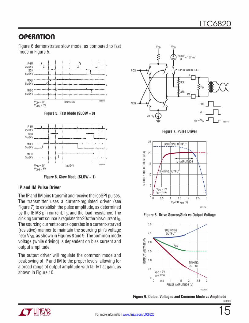
IP and IM Pulse Driver
The IP and IM pins transmit and receive the isoSPI pulses. The transmitter uses a current-regulated driver (see Figure 7) to establish the pulse amplitude, as determined by the IBIAS pin current, IB, and the load resistance. The sinking current source is regulated to 20x the bias current IB. The sourcing current source operates in a current-starved (resistive) manner to maintain the sourcing pin’s voltage near VDD, as shown in Figures 8 and 9. The common mode voltage (while driving) is dependent on bias current and output amplitude.
The output driver will regulate the common mode and peak swing of IP and IM to the proper levels, allowing for a broad range of output amplitude with fairly flat gain, as shown in Figure 10.
+–
RM
35k
OPEN WHEN IDLE
+ 167mV
VDD VDD
35k
6820 F07
POS
NEG
20 • IB
POS
NEG
VIP – VIM
IP
VICMP3
IM
Figure 7. Pulse Driver
VIP OR VIM (V)0
0
SOUR
CE/S
INK
CURR
ENT
(mA)
5
10
15
20
25
0.5 1 1.5 2
6820 F08
2.5 3
SOURCING OUTPUT
1V AMPLITUDE
SINKING OUTPUT
VDD = 3VIB = 1mA
Figure 8. Drive Source/Sink vs Output Voltage
PULSE AMPLITUDE (V)0
0
OUTP
UT V
OLTA
GE (V
)
0.5
1.0
1.5
2.0
3.0
VCM
0.5 1 1.5 2
6820 F09
2.5 3
2.5SOURCING
OUTPUT
SINKINGOUTPUT
VDD = 3VIB = 1mA
Figure 9. Output Voltages and Common Mode vs Amplitude
LTC6820
166820fb
For more information www.linear.com/LTC6820
OPERATION
Figure 10. AIB Current Gain vs Amplitude
PULSE AMPLITUDE (V)0
0
CURR
ENT
GAIN
(mA/
mA)
5
10
15
20
25
0.5 1 1.5 2
6820 F10
2.5 3
VDD = 3VIS = 1mA
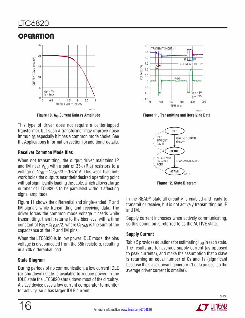
This type of driver does not require a center-tapped transformer, but such a transformer may improve noise immunity, especially if it has a common mode choke. See the Applications Information section for additional details.
Receiver Common Mode Bias
When not transmitting, the output driver maintains IP and IM near VDD with a pair of 35k (RIN) resistors to a voltage of VDD – VICMP/3 – 167mV. This weak bias net-work holds the outputs near their desired operating point without significantly loading the cable, which allows a large number of LTC6820’s to be paralleled without affecting signal amplitude.
Figure 11 shows the differential and single-ended IP and IM signals while transmitting and receiving data. The driver forces the common mode voltage it needs while transmitting, then it returns to the bias level with a time constant of RIN • CLOAD/2, where CLOAD is the sum of the capacitance at the IP and IM pins.
When the LTC6820 is in low power IDLE mode, the bias voltage is disconnected from the 35k resistors, resulting in a 70k differential load.
State Diagram
During periods of no communication, a low current IDLE (or shutdown) state is available to reduce power. In the IDLE state the LTC6820 shuts down most of the circuitry. A slave device uses a low current comparator to monitor for activity, so it has larger IDLE current.
Figure 11. Transmitting and Receiving Data
Figure 12. State Diagram
TIME (ns)0
–1.5
VOLT
AGE
(V)
–1.0
0
0.5
1.0
400 800 1000
3.0
IP IM
IP-IM
6820 F11
–0.5
200 600
1.5
2.0
2.5TRANSMIT SHORT +1
RECEIVE SHORT –1
VDD = 3VIB = 1mA
IDLE
READY
WAKE-UP SIGNAL(tREADY)
IDLETIMEOUT(tIDLE)
NO ACTIVITYON isoSPIPORT
TRANSMIT/RECEIVE
6820 F12ACTIVE
In the READY state all circuitry is enabled and ready to transmit or receive, but is not actively transmitting on IP and IM.
Supply current increases when actively communicating, so this condition is referred to as the ACTIVE state.
Supply Current
Table 5 provides equations for estimating IDD in each state. The results are for average supply current (as opposed to peak currents), and make the assumption that a slave is returning an equal number of 0s and 1s (significant because the slave doesn’t generate +1 data pulses, so the average driver current is smaller).
LTC6820
176820fb
For more information www.linear.com/LTC6820
OPERATIONTable 5. IDD Equations
STATE MSTR ESTIMATED IDD
IDLE 0 (slave) 2µA
1 (master) 1µA
READY 0 or 1 1.7mA + 3 • IBACTIVE 0 (slave)
2mA + 3 + 20 •
100ns • 0.5tCLK
• IB
1 (master)
2mA + 3 + 20 •
100nstCLK
• IB
IDLE Mode and Wake-Up Detection
To conserve power, an LTC6820 in slave mode (MSTR = 0) will enter an IDLE state after 5.7ms (tIDLE) of inactivity on the IP/IM pins. In this condition IDD is reduced to less than 6µA and the SPI pins are idled (CS = 1, MOSI = 1 and SCK = POL).
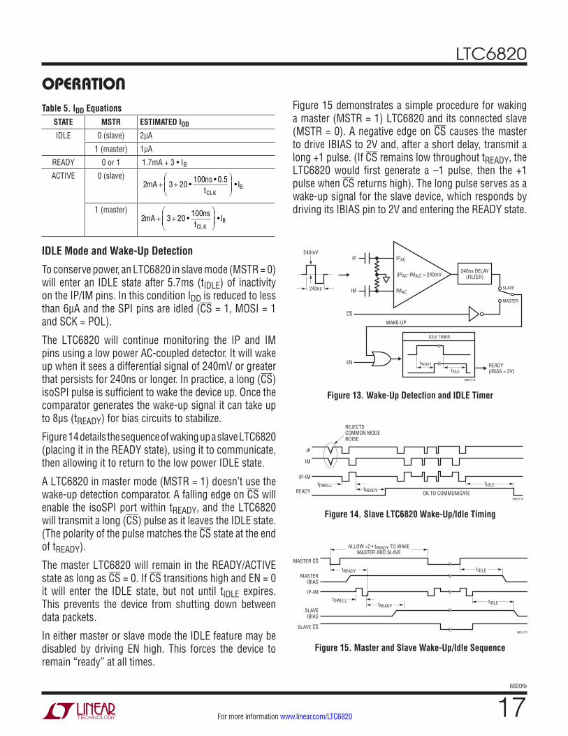
The LTC6820 will continue monitoring the IP and IM pins using a low power AC-coupled detector. It will wake up when it sees a differential signal of 240mV or greater that persists for 240ns or longer. In practice, a long (CS) isoSPI pulse is sufficient to wake the device up. Once the comparator generates the wake-up signal it can take up to 8µs (tREADY) for bias circuits to stabilize.
Figure 14 details the sequence of waking up a slave LTC6820 (placing it in the READY state), using it to communicate, then allowing it to return to the low power IDLE state.
A LTC6820 in master mode (MSTR = 1) doesn’t use the wake-up detection comparator. A falling edge on CS will enable the isoSPI port within tREADY, and the LTC6820 will transmit a long (CS) pulse as it leaves the IDLE state. (The polarity of the pulse matches the CS state at the end of tREADY).
The master LTC6820 will remain in the READY/ACTIVE state as long as CS = 0. If CS transitions high and EN = 0 it will enter the IDLE state, but not until tIDLE expires. This prevents the device from shutting down between data packets.
In either master or slave mode the IDLE feature may be disabled by driving EN high. This forces the device to remain “ready” at all times.
Figure 15 demonstrates a simple procedure for waking a master (MSTR = 1) LTC6820 and its connected slave (MSTR = 0). A negative edge on CS causes the master to drive IBIAS to 2V and, after a short delay, transmit a long +1 pulse. (If CS remains low throughout tREADY, the LTC6820 would first generate a –1 pulse, then the +1 pulse when CS returns high). The long pulse serves as a wake-up signal for the slave device, which responds by driving its IBIAS pin to 2V and entering the READY state.
|IPAC–IMAC| > 240mV
IPAC
IMAC
WAKE-UP
IP240mV
IM
EN
CS
240ns
240ns DELAY(FILTER)
SLAVE
MASTER
tREADY
tIDLE
IDLE TIMER
READY(IBIAS = 2V)
6820 F13
Figure 13. Wake-Up Detection and IDLE Timer
Figure 14. Slave LTC6820 Wake-Up/Idle Timing
Figure 15. Master and Slave Wake-Up/Idle Sequence
REJECTSCOMMON MODENOISE
IP
IM
IP-IM
READYtDWELL
tREADYtIDLE
6820 F14
OK TO COMMUNICATE
SLAVE CS
SLAVEIBIAS
IP-IM
MASTERIBIAS
MASTER CS
tDWELL
ALLOW >2 • tREADY TO WAKEMASTER AND SLAVE
tREADY
6820 F15
tIDLE
tIDLEtREADY
LTC6820
186820fb
For more information www.linear.com/LTC6820
IP
RM
LTC6820
MSTRMOSIMISOSCKCS
IM
MASTER
SDOSDISCK
CS
1
1 1
2 2
3 3
2
3
IPMSTR
MOSIMISO
SCKCS
IM
SLAVE 1LTC6820
SDISDOSCKCS
IPMSTR
MOSIMISO
SCKCS
IM
SLAVE 2LTC6820
SDISDOSCKCS
RM
IPMSTR
MOSIMISO
SCKCS
IM
SLAVE 3
6820 F16
LTC6820
SDISDOSCKCS
Figure 16. Multidropping Multiple Slaves on a Single Cable
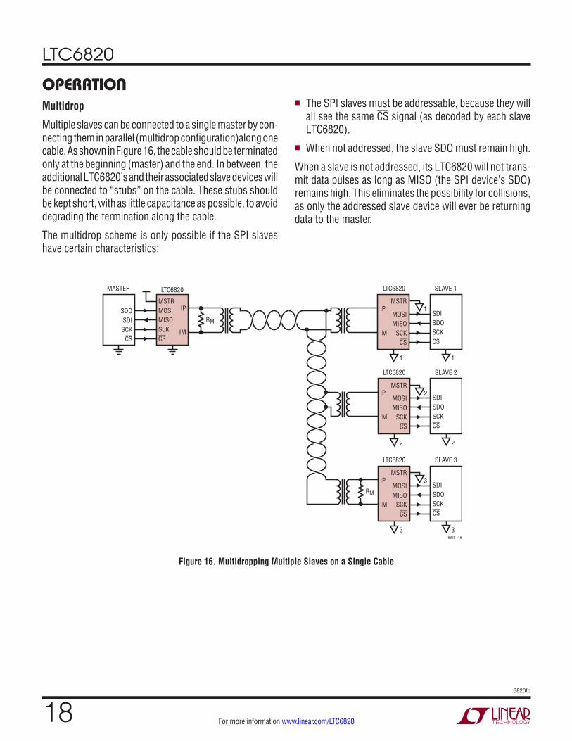
OPERATIONMultidrop
Multiple slaves can be connected to a single master by con-necting them in parallel (multidrop configuration)along one cable. As shown in Figure 16, the cable should be terminated only at the beginning (master) and the end. In between, the additional LTC6820’s and their associated slave devices will be connected to “stubs” on the cable. These stubs should be kept short, with as little capacitance as possible, to avoid degrading the termination along the cable.
The multidrop scheme is only possible if the SPI slaves have certain characteristics:
n The SPI slaves must be addressable, because they will all see the same CS signal (as decoded by each slave LTC6820).
n When not addressed, the slave SDO must remain high.
When a slave is not addressed, its LTC6820 will not trans-mit data pulses as long as MISO (the SPI device’s SDO) remains high. This eliminates the possibility for collisions, as only the addressed slave device will ever be returning data to the master.
LTC6820
196820fb
For more information www.linear.com/LTC6820
APPLICATIONS INFORMATIONisoSPI Setup
The LTC6820 allows each application to be optimized for power consumption or for noise immunity. The power and noise immunity of an isoSPI system is determined by the programmed IB current. The IB current can range from 0.1mA to 1mA. A low IB reduces the isoSPI power consumption in the READY and ACTIVE states, while a high IB increases the amplitude of the differential signal voltage VA across the matching termination resistor, RM.
IB is programmed by the sum of the RB1 and RB2 resis-tors connected between the IBIAS pin and GND. For most applications setting IB to 0.5mA is a good compromise between power consumption and noise immunity. Using this IB setting with a 1:1 transformer and RM = 120Ω, RB1 should be set to 2.8k and RB2 set to 1.2k. In a typical CAT5 twisted pair these settings will allow for communication up to 50m.
For applications that require cables longer than 50m it is recommended to increase the amplitude VA by increasing IB to 1mA. This compensates for the increased insertion loss in the cable and maintains high noise immunity. So when using cables over 50m and, again, using a trans-former with a 1:1 turns ratio and RM = 120Ω, RB1 would be 1.4k and RB2 would be 600Ω.
Other IB settings can be used to reduce power consumption or increase the noise immunity as required by the applica-tion. In these cases when setting VICMP and choosing RB1 and RB2 resistor values the following rules should be used:
For cables 50 meters or less:
IB = 0.5mA
VA = (20 • IB) • (RM/2)
VTCMP = 1/2 • VA
VICMP = 2 • VTCMP
RB2 = VICMP/IB
RB1 =
2VIB
– RB2
For cables over 50 meters:
IB = 1mA
VA = (20 • IB) • (RM/2)
VTCMP = 1/4 • VA
VICMP = 2 • VTCMP
RB2 = VICMP/IB
RB1 =
2VIB
– RB2
The maximum data rate of an isoSPI link is determined by the length of the cable used. For cables 10 meters or less the maximum 1MHz SPI clock frequency is possible. As the length of the cable increases the maximum possible SPI clock rate decreases. This is a result of the increased propagation delays through the cable creating possible timing violations.
Cable delay affects three timing specifications, tCLK, t6, and t7. In the Electrical Characteristics table, each is derated by 100ns to allow for 50ns of cable delay. For longer cables, the minimum timing parameters may be calculated as shown below:
tCLK, t6, and t7 > 0.9µs + 2 • tCABLE
Pull-Up Resistance Considerations
The data output (MOSI if MSTR = 0, MISO if MSTR = 1) requires a pull-up resistor, RPU. The rise time tRISE is determined by RPU and the capacitance on the pin. RPU must be small enough to provide adequate setup and hold times. For a slave device, the time constant must be less than t12 and t14. In fast mode, 50ns is recommended.
RPU < 50ns/CLOAD
Larger pull-up resistances, up to 5k, can be used in slow mode.
LTC6820
206820fb
For more information www.linear.com/LTC6820
APPLICATIONS INFORMATION
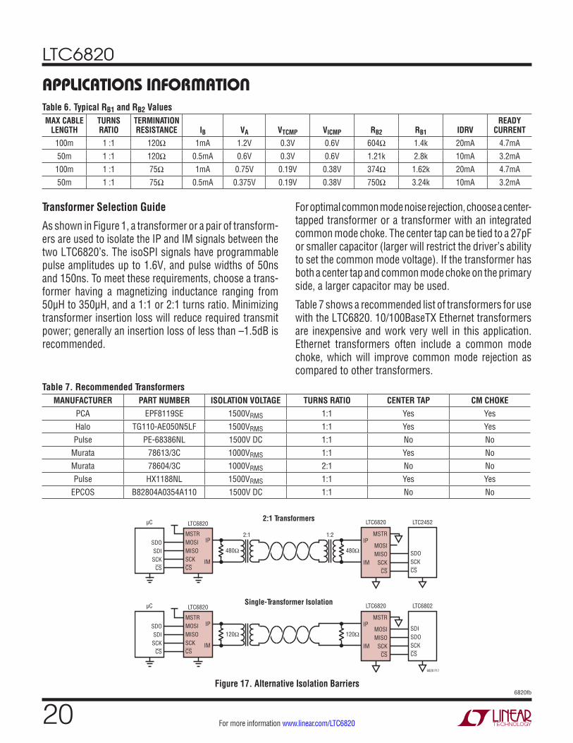
Transformer Selection Guide
As shown in Figure 1, a transformer or a pair of transform-ers are used to isolate the IP and IM signals between the two LTC6820’s. The isoSPI signals have programmable pulse amplitudes up to 1.6V, and pulse widths of 50ns and 150ns. To meet these requirements, choose a trans-former having a magnetizing inductance ranging from 50µH to 350µH, and a 1:1 or 2:1 turns ratio. Minimizing transformer insertion loss will reduce required transmit power; generally an insertion loss of less than –1.5dB is recommended.
For optimal common mode noise rejection, choose a center-tapped transformer or a transformer with an integrated common mode choke. The center tap can be tied to a 27pF or smaller capacitor (larger will restrict the driver’s ability to set the common mode voltage). If the transformer has both a center tap and common mode choke on the primary side, a larger capacitor may be used.
Table 7 shows a recommended list of transformers for use with the LTC6820. 10/100BaseTX Ethernet transformers are inexpensive and work very well in this application. Ethernet transformers often include a common mode choke, which will improve common mode rejection as compared to other transformers.
Table 6. Typical RB1 and RB2 ValuesMAX CABLE
LENGTHTURNS RATIO
TERMINATION RESISTANCE IB VA VTCMP VICMP RB2 RB1 IDRV
READY CURRENT
100m 1 :1 120Ω 1mA 1.2V 0.3V 0.6V 604Ω 1.4k 20mA 4.7mA
50m 1 :1 120Ω 0.5mA 0.6V 0.3V 0.6V 1.21k 2.8k 10mA 3.2mA
100m 1 :1 75Ω 1mA 0.75V 0.19V 0.38V 374Ω 1.62k 20mA 4.7mA
50m 1 :1 75Ω 0.5mA 0.375V 0.19V 0.38V 750Ω 3.24k 10mA 3.2mA
Table 7. Recommended TransformersMANUFACTURER PART NUMBER ISOLATION VOLTAGE TURNS RATIO CENTER TAP CM CHOKE
PCA EPF8119SE 1500VRMS 1:1 Yes Yes
Halo TG110-AE050N5LF 1500VRMS 1:1 Yes Yes
Pulse PE-68386NL 1500V DC 1:1 No No
Murata 78613/3C 1000VRMS 1:1 Yes No
Murata 78604/3C 1000VRMS 2:1 No No
Pulse HX1188NL 1500VRMS 1:1 Yes Yes
EPCOS B82804A0354A110 1500V DC 1:1 No No
IP
480Ω
LTC6820
2:1 1:2MSTRMOSIMISOSCKCS
IM
µC
SDOSDISCK
CS
480Ω
IPMSTR
MOSIMISO
SCKCS
IM
LTC2452LTC68202:1 Transformers
SDOSCKCS
IP
120Ω
LTC6820
MSTRMOSIMISOSCKCS
IM
µC
SDOSDISCK
CS
120Ω
6820 F17
IPMSTR
MOSIMISO
SCKCS
IM
LTC6802LTC6820Single-Transformer Isolation
SDISDOSCKCS
Figure 17. Alternative Isolation Barriers
LTC6820
216820fb
For more information www.linear.com/LTC6820
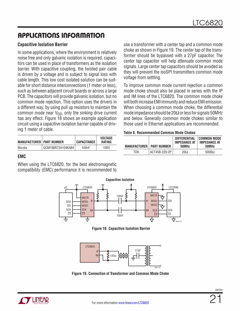
APPLICATIONS INFORMATIONCapacitive Isolation Barrier
In some applications, where the environment is relatively noise free and only galvanic isolation is required, capaci-tors can be used in place of transformers as the isolation barrier. With capacitive coupling, the twisted pair cable is driven by a voltage and is subject to signal loss with cable length. This low cost isolated solution can be suit-able for short distance interconnections (1 meter or less), such as between adjacent circuit boards or across a large PCB. The capacitors will provide galvanic isolation, but no common mode rejection. This option uses the drivers in a different way, by using pull up resistors to maintain the common mode near VDD, only the sinking drive current has any effect. Figure 18 shows an example application circuit using a capacitive isolation barrier capable of driv-ing 1 meter of cable.
MANUFACTURER PART NUMBER CAPACITANCEVOLTAGE RATING
Murata GCM188R72A104KA64 100nF 100V
EMC
When using the LTC6820, for the best electromagnetic compatibility (EMC) performance it is recommended to
use a transformer with a center tap and a common mode choke as shown in Figure 19. The center tap of the trans-former should be bypassed with a 27pF capacitor. The center tap capacitor will help attenuate common mode signals. Large center tap capacitors should be avoided as they will prevent the isoSPI transmitters common mode voltage from settling.
To improve common mode current rejection a common mode choke should also be placed in series with the IP and IM lines of the LTC6820. The common mode choke will both increase EMI immunity and reduce EMI emission. When choosing a common mode choke, the differential mode impedance should be 20Ω or less for signals 50MHz and below. Generally common mode chokes similar to those used in Ethernet applications are recommended.
Table 8. Recommended Common Mode Chokes
MANUFACTURER PART NUMBER
DIFFERENTIAL IMPEDANCE AT
50MHz
COMMON MODE IMPEDANCE AT
50MHz
TDK ACT45B-220-2P 20Ω 5000Ω
LTC6820µC
MSTR
MOSIMISO
SCKCS
LTC2640LTC6820
SDIIP
100nF
Capacitive Isolation
IM
MSTRMOSIMISOSCKCS
IP
IM SCKCS100nF
6820 F18
SDOSDISCK
CS
Figure 18. Capacitive Isolation Barrier
120Ω
IPIM
LTC6820
6820 F19
27pF
Figure 19. Connection of Transformer and Common Mode Choke
LTC6820
226820fb
For more information www.linear.com/LTC6820
APPLICATIONS INFORMATION
Figure 20. Example Layout
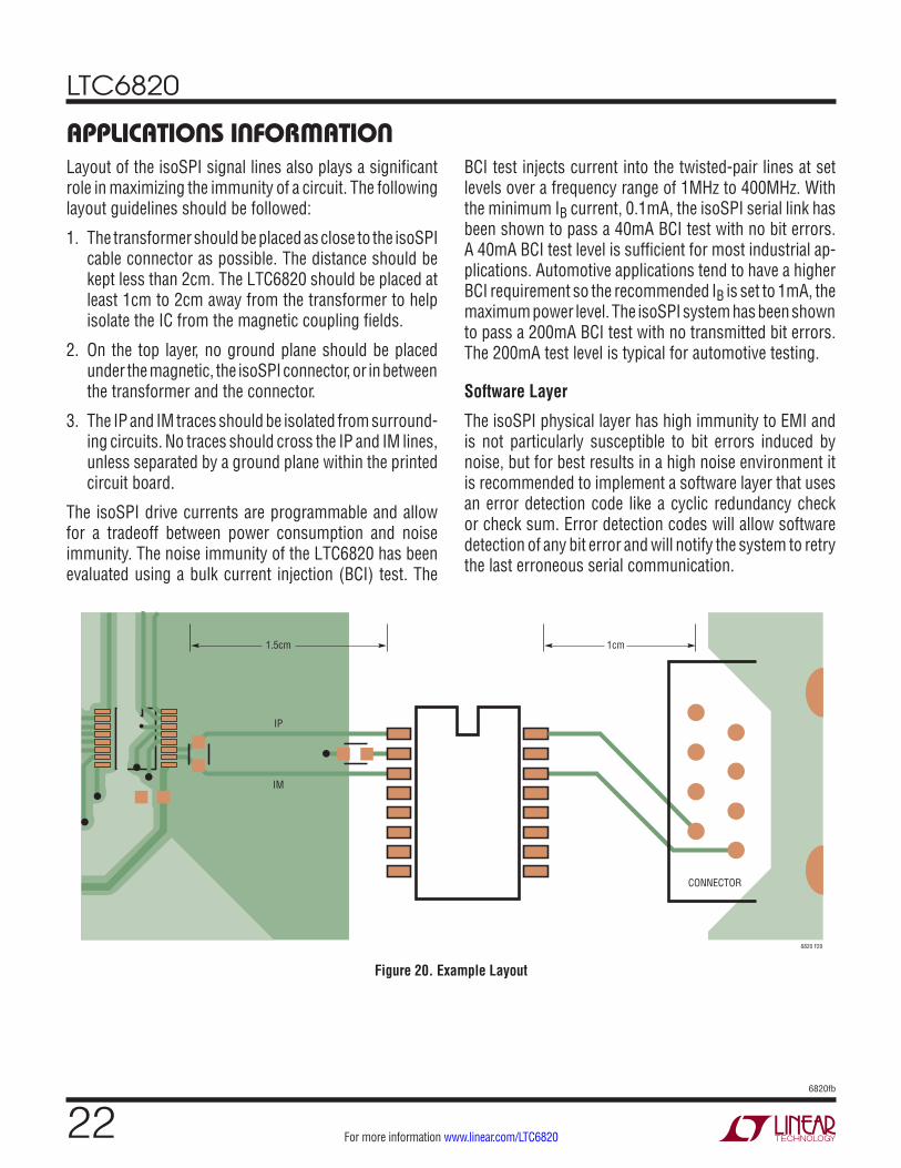
Layout of the isoSPI signal lines also plays a significant role in maximizing the immunity of a circuit. The following layout guidelines should be followed:
1. The transformer should be placed as close to the isoSPI cable connector as possible. The distance should be kept less than 2cm. The LTC6820 should be placed at least 1cm to 2cm away from the transformer to help isolate the IC from the magnetic coupling fields.
2. On the top layer, no ground plane should be placed under the magnetic, the isoSPI connector, or in between the transformer and the connector.
3. The IP and IM traces should be isolated from surround-ing circuits. No traces should cross the IP and IM lines, unless separated by a ground plane within the printed circuit board.
The isoSPI drive currents are programmable and allow for a tradeoff between power consumption and noise immunity. The noise immunity of the LTC6820 has been evaluated using a bulk current injection (BCI) test. The
BCI test injects current into the twisted-pair lines at set levels over a frequency range of 1MHz to 400MHz. With the minimum IB current, 0.1mA, the isoSPI serial link has been shown to pass a 40mA BCI test with no bit errors. A 40mA BCI test level is sufficient for most industrial ap-plications. Automotive applications tend to have a higher BCI requirement so the recommended IB is set to 1mA, the maximum power level. The isoSPI system has been shown to pass a 200mA BCI test with no transmitted bit errors. The 200mA test level is typical for automotive testing.
Software Layer
The isoSPI physical layer has high immunity to EMI and is not particularly susceptible to bit errors induced by noise, but for best results in a high noise environment it is recommended to implement a software layer that uses an error detection code like a cyclic redundancy check or check sum. Error detection codes will allow software detection of any bit error and will notify the system to retry the last erroneous serial communication.
1.5cm
IP
IM
1cm
CONNECTOR
6820 F20
LTC6820
236820fb
For more information www.linear.com/LTC6820
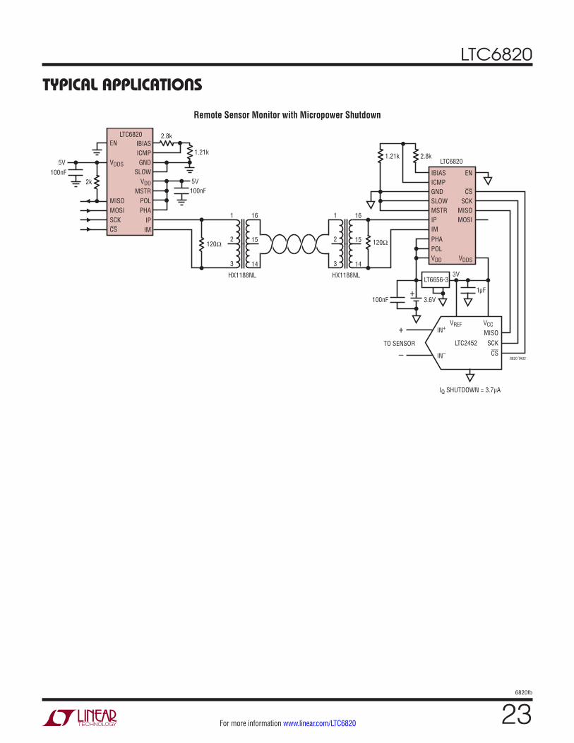
TYPICAL APPLICATIONS
15
HX1188NL HX1188NL
120Ω
1.21k 2.8k
100nF
2
1
3
2
1
314
16
15
14
16
100nF IBIASICMPGNDSLOWMSTRIPIM
EN
CSSCK
MISOMOSI
PHA
VDDS
POLVDD
1µF
3V
100nF
+
–TO SENSOR SCK
MISOIN+
IN– CS6820 TA02
3.6V
LTC6820
+LT6656-3
VCCVREF
LTC2452
2.8k
1.21k
5V
LTC6820
IQ SHUTDOWN = 3.7µA
120Ω
2k
IBIASICMPGND
SLOWVDD
IPIM
POLMSTR
PHA
EN
MISOMOSISCKCS
VDDS5V
Remote Sensor Monitor with Micropower Shutdown
LTC6820
246820fb
For more information www.linear.com/LTC6820
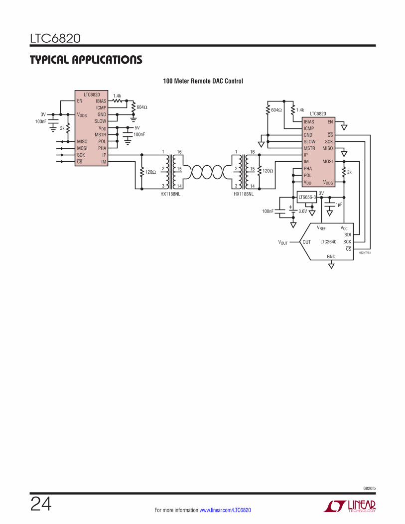
100 Meter Remote DAC Control
15
HX1188NL HX1188NL
120Ω
604Ω 1.4k
100nF
2
1
3
2
1
314
16
15
14
16
100nF IBIASICMPGNDSLOWMSTRIPIM
EN
CSSCK
MISO
PHA
VDDS
MOSI
POLVDD
1µF
3V
100nF
VOUT SCKSDI
CS6820 TA03
3.6V
LTC6820
+LT6656-3
VCC
GND
VREF
LTC2640
1.4k
604Ω
5V
LTC6820
120Ω
2k
IBIASICMPGND
SLOWVDD
IPIM
POLMSTR
PHA
EN
MISOMOSISCKCS
VDDS3V
OUT
2k
TYPICAL APPLICATIONS
LTC6820
256820fb
For more information www.linear.com/LTC6820
806Ω
1.21k
IPA
IBIAS
IMA
ICMP
VM
6820 TA05
LTC6804-2
120Ω
VREGISOMDA3A2A1A0
VREGISOMDA3A2A1A0
806Ω
1.21k
IPA
IBIAS
IMA
ICMP
VM
LTC6804-2
1
2
0
806Ω
1.21k
IPA
IBIAS
IMA
ICMP
VM
LTC6804-2VREGISOMDA3A2A1A0
1
2
0
100nF
100nF
806Ω
1.21k
5V
LTC6820
120Ω
2k
IBIASICMPGND
SLOWVDD
IPIM
POLMSTR
PHA
EN
MISOMOSISCKCS
VDDS5V
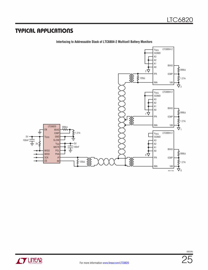
Interfacing to Addressable Stack of LTC6804-2 Multicell Battery Monitors
TYPICAL APPLICATIONS
LTC6820
266820fb
For more information www.linear.com/LTC6820
TYPICAL APPLICATIONS
120Ω 2k
100Ω806Ω1.21k
IBIASICMPGNDSLOWMSTR
LTC6820 GND3
GND3
LTC6803-2 VSTACK3
VREG CZT3055MOSIMISOSCKCS
A3A2A1A0
2k
100Ω
806Ω1.21k
806Ω1.21k
VDD2
VDD2
VDD1
VDD1
IBIASICMPGNDSLOWMSTR
ENMOSIMISO
SCKCS
LTC6820
LTC6803-2
GND2
GND2
GND1
GND1
GND1
GND2
GND3
VSTACK2
VREG CZT3055MOSIMISOSCKCS
A3A2A1A0
2k
100ΩIBIASICMPGNDSLOWMSTR
ENMOSIMISO
SCKCS
LTC6820
LTC6803-2 VSTACK1
VREG CZT3055
6820 TA04
MOSIMISOSCKCS
A3A2A1A0
VDD3
VDD3
100nF
100nF
806Ω
1.21k
5V
LTC6820
120Ω
2k
IBIASICMPGND
SLOWVDD
IPIM
POLMSTR
PHA
EN
MISOMOSISCKCS
VDDS5V
ENMOSIMISO
SCKCS
VDDSPOLPHA
VDDSPOLPHA
VDDSPOLPHA
IPIMVDD
IPIMVDD
IPIMVDD
2k
2k
2k
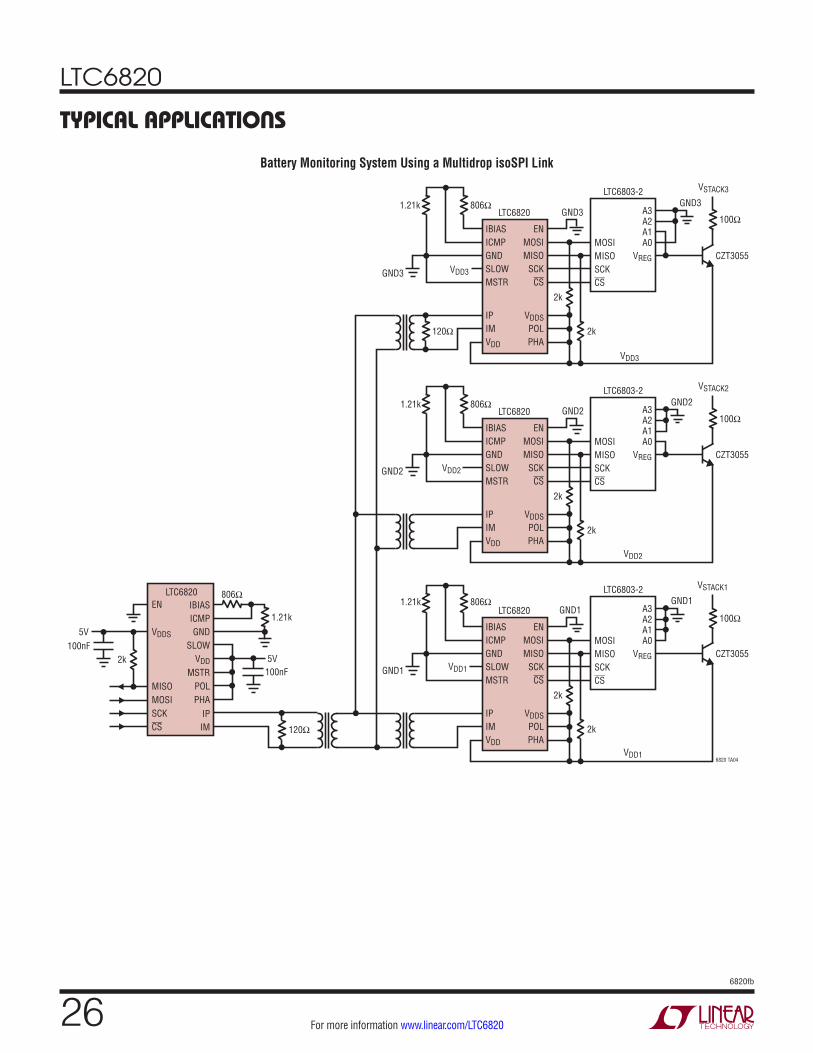
Battery Monitoring System Using a Multidrop isoSPI Link
LTC6820
276820fb
For more information www.linear.com/LTC6820
PACKAGE DESCRIPTION
3.00 ±0.10(4 SIDES)
RECOMMENDED SOLDER PAD PITCH AND DIMENSIONS
1.65 ±0.05(4 SIDES)
NOTE:1. DRAWING CONFORMS TO JEDEC PACKAGE OUTLINE MO-220 VARIATION (WEED-4)2. DRAWING NOT TO SCALE3. ALL DIMENSIONS ARE IN MILLIMETERS4. DIMENSIONS OF EXPOSED PAD ON BOTTOM OF PACKAGE DO NOT INCLUDE MOLD FLASH. MOLD FLASH, IF PRESENT, SHALL NOT EXCEED 0.15mm ON ANY SIDE5. EXPOSED PAD SHALL BE SOLDER PLATED6. SHADED AREA IS ONLY A REFERENCE FOR PIN 1 LOCATION ON THE TOP AND BOTTOM OF PACKAGE
PIN 1TOP MARK(NOTE 6)
0.40 ±0.10
BOTTOM VIEW—EXPOSED PAD
1.65 ±0.10(4-SIDES)
0.75 ±0.05 R = 0.115TYP
0.25 ±0.05
1
PIN 1 NOTCH R = 0.20 TYPOR 0.25 × 45° CHAMFER
15 16
2
0.50 BSC
0.200 REF
2.10 ±0.053.50 ±0.05
0.70 ±0.05
0.00 – 0.05
(UD16 VAR A) QFN 1207 REV A
0.25 ±0.050.50 BSC
PACKAGE OUTLINE
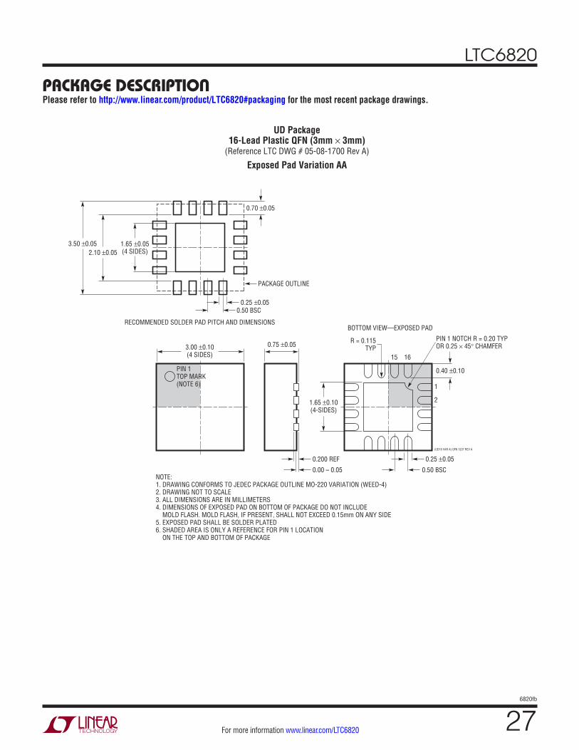
UD Package16-Lead Plastic QFN (3mm × 3mm)
(Reference LTC DWG # 05-08-1700 Rev A)
Exposed Pad Variation AA
Please refer to http://www.linear.com/product/LTC6820#packaging for the most recent package drawings.
LTC6820
286820fb
For more information www.linear.com/LTC6820
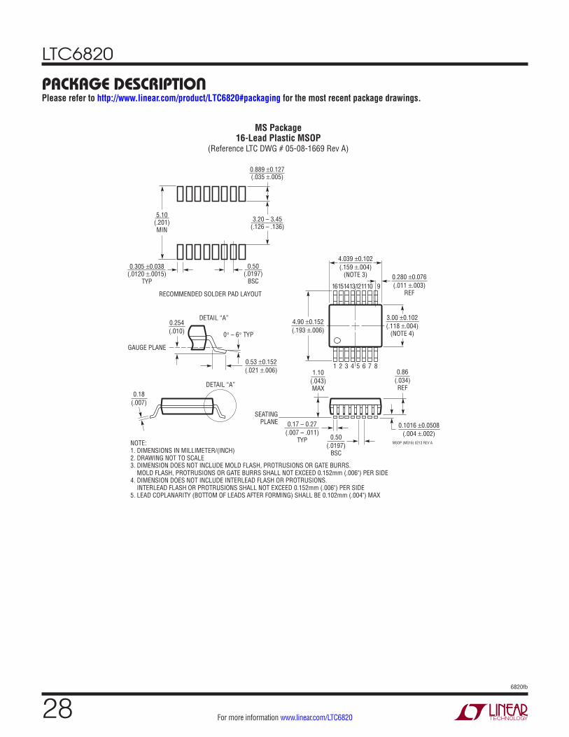
PACKAGE DESCRIPTION
MSOP (MS16) 0213 REV A
0.53 ±0.152(.021 ±.006)
SEATINGPLANE
0.18(.007)
1.10(.043)MAX
0.17 – 0.27(.007 – .011)
TYP
0.86(.034)REF
0.50(.0197)
BSC
16151413121110
1 2 3 4 5 6 7 8
9
NOTE:1. DIMENSIONS IN MILLIMETER/(INCH)2. DRAWING NOT TO SCALE3. DIMENSION DOES NOT INCLUDE MOLD FLASH, PROTRUSIONS OR GATE BURRS. MOLD FLASH, PROTRUSIONS OR GATE BURRS SHALL NOT EXCEED 0.152mm (.006") PER SIDE4. DIMENSION DOES NOT INCLUDE INTERLEAD FLASH OR PROTRUSIONS. INTERLEAD FLASH OR PROTRUSIONS SHALL NOT EXCEED 0.152mm (.006") PER SIDE5. LEAD COPLANARITY (BOTTOM OF LEADS AFTER FORMING) SHALL BE 0.102mm (.004") MAX
0.254(.010) 0° – 6° TYP
DETAIL “A”
DETAIL “A”
GAUGE PLANE
5.10(.201)MIN
3.20 – 3.45(.126 – .136)
0.889 ±0.127(.035 ±.005)
RECOMMENDED SOLDER PAD LAYOUT
0.305 ±0.038(.0120 ±.0015)
TYP
0.50(.0197)
BSC
4.039 ±0.102(.159 ±.004)
(NOTE 3)
0.1016 ±0.0508(.004 ±.002)
3.00 ±0.102(.118 ±.004)
(NOTE 4)
0.280 ±0.076(.011 ±.003)
REF
4.90 ±0.152(.193 ±.006)
MS Package16-Lead Plastic MSOP
(Reference LTC DWG # 05-08-1669 Rev A)
Please refer to http://www.linear.com/product/LTC6820#packaging for the most recent package drawings.
LTC6820
296820fb
For more information www.linear.com/LTC6820
Information furnished by Linear Technology Corporation is believed to be accurate and reliable. However, no responsibility is assumed for its use. Linear Technology Corporation makes no representa-tion that the interconnection of its circuits as described herein will not infringe on existing patent rights.
REVISION HISTORYREV DATE DESCRIPTION PAGE NUMBER
A 06/13 Web hyperlinks added.Note 8 added to Electrical Characteristics section.
1 to 305
B 01/17 Patent Information added. Web Links updated.
1 All
LTC6820
306820fb
For more information www.linear.com/LTC6820 LINEAR TECHNOLOGY CORPORATION 2012
LT 0117 REV B• PRINTED IN USALinear Technology Corporation1630 McCarthy Blvd., Milpitas, CA 95035-7417(408) 432-1900 ● FAX: (408) 434-0507 ● www.linear.com/LTC6820
TYPICAL APPLICATION
RELATED PARTSPART NUMBER DESCRIPTION COMMENTS
LTC6803-2/LTC6803-4
Multicell Battery Stack Monitor with an Individually Addressable SPI Interface
Functionality Equivalent to LTC6803-1/LTC6803-3, Allows for Parallel Communication Battery Stack Topologies
LTC6803-1/LTC6803-3
Multicell Battery Stack Monitor with Daisy-Chained SPI Interface
Functionality Equivalent to LTC6803-2/LTC6803-4, Allows for Multiple Devices to Be Daisy Chained
LTC6903 1kHz to 68MHz Programmable Silicon Oscillator with SPI Interface
Frequency Resolution of 0.01%. No External Components Required. Operates on 2.7V to 5.5V.
LTC6804-1/LTC6804-2
Multicell Battery Stack Monitor with Built-In isoSPI Interface
Includes isoSPI Interfaces for Communication with Master LTC6820 and to other LTC6804 Devices
806Ω
1.21k
IPA
IBIAS
IMA
ICMP
VM
6820 TA06
LTC6804-1
120Ω
120Ω
120Ω
VREGISOMD
806Ω
1.21k
IPA
IBIAS
IMA
ICMP
VM
GND3
GND2
IPB
IMB
IPB
IMB
LTC6804-1
120Ω
120Ω
VREGISOMD
806Ω
1.21k
IPA
IBIAS
IMA
ICMP
VM
GND4
IPB
IMB
LTC6804-1 VREGISOMD
100nF
100nF
806Ω
1.21k
5V
LTC6820
120Ω
2k
IBIASICMPGND
SLOWVDD
IPIM
POLMSTR
PHA
EN
MISOMOSISCKCS
VDDS5V
Interfacing to Daisy-Chained Stack of LTC6804-1 Multicell Battery Monitors