Embed Size (px)
Citation preview

LTC6810-1/LTC6810-2
1Rev 0
For more information www.analog.comDocument Feedback
TYPICAL APPLICATION
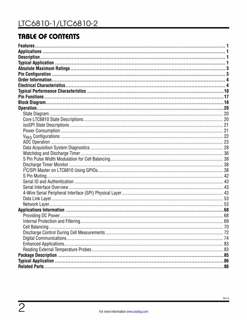
FEATURES DESCRIPTION
6-Channel Battery Stack Monitors
The LTC®6810 is a multicell battery stack monitor. The LTC6810 measures up to 6 series-connected battery cells with a total measurement error of less than 1.8mV. The cell measurement range of 0V to 5V makes the LTC6810 suitable for most battery chemistries. All 6 cells can be measured in 290µs, and lower data acquisition rates can be selected for high noise reduction.
Multiple LTC6810-1 devices can be connected in series, permitting simultaneous cell monitoring of long, high voltage battery strings. Each LTC6810 has an isoSPI interface for high speed, RF-immune, long distance com-munications. Using the LTC6810-1, multiple devices are connected in a daisy chain with one host processor con-nection for all devices. The LTC6810-1 supports bidi-rectional operation, allowing communication even with a broken wire. Using the LTC6810-2, multiple devices are connected in parallel to the host processor, with each device individually addressed.
The LTC6810 can be powered directly from the battery stack or from an isolated supply. The LTC6810 includes passive balancing for each cell, with PWM duty cycle control for each cell and the ability to perform redundant cell measurements. Other features include an onboard 5V regulator, 4 general purpose I/O lines and a sleep mode in which current consumption is reduced to 4µA.
APPLICATIONS
n Measures Up to 6 Battery Cells in Series n 1.8mV Maximum Total Measurement Error n Stackable Architecture Supports 100s of Cells n Built-in isoSPI™ Interface n 290µs to Measure All Cells in a System.
n 1Mb Isolated Serial Communications n Uses Single Twisted Pair, Up to 100 Meters n Low EMI Susceptibility and Emissions n Bidirectional for Broken Wire Protection
n Guaranteed Performance Down to 5V n Performs Redundant Cell Measurements. n Engineered for ISO 26262 Compliant Systems n Passive Cell Balancing with Programmable Pulse
Width Modulation n 4 General Purpose Digital I/O or Analog Inputs
n Temperature or Other Sensor Inputs n Configurable as an I2C or SPI master
n 4μA Sleep Mode Supply Current n 44-Lead SSOP Package
n Electric and Hybrid Electric Vehicles n Backup Battery Systems n Grid Energy Storage n High Power Portable Equipment
All registered trademarks and trademarks are the property of their respective owners.
LTC6810
68101 TA01a
16-BIT ∆ WITHPROGRAMMABLE
NOISE FILTER
+
MUX
MUX
LOGIC
SERIALPORT B
SERIALPORT A
UNIQUE ID
DIE TEMP
SECONDREFERENCE
FIRSTREFERENCE
OPTIONALEEPROM
CURRENTSENSOR
REVERSIBLE
4-WIRESPI
isoSPI
isoSPI
10kNTC
–
4 GENERAL PURPOSEANALOG IN ANDDIGITAL IN/OUT
MEASUREMENT ERROR OFCELL1 WITH 3.3V INPUT,VREG INTERNALLY GENERATED,FIGURE 2
V+ (V)
5 10 15 20 25 30–2.0
–1.5
–1.0
–0.5
0
0.5
1.0
1.5
2.0
MEA
SURE
MEN
T ER
ROR
(mV)
125°C25°C–40°C
6810 TA01b
Measurement Error vs V+
LTC6810-1/LTC6810-2
2Rev 0
For more information www.analog.com
TABLE OF CONTENTS Features ............................................................................................................................ 1Applications ....................................................................................................................... 1Description......................................................................................................................... 1Typical Application ............................................................................................................... 1Absolute Maximum Ratings ..................................................................................................... 3Pin Configuration ................................................................................................................. 3Order Information ................................................................................................................. 4Electrical Characteristics ........................................................................................................ 4Typical Performance Characteristics .........................................................................................10Pin Functions .....................................................................................................................17Block Diagram ....................................................................................................................18Operation..........................................................................................................................20
State Diagram ....................................................................................................................................................... 20Core LTC6810 State Descriptions ......................................................................................................................... 20isoSPI State Descriptions ..................................................................................................................................... 21Power Consumption ............................................................................................................................................. 21VREG Configurations ............................................................................................................................................. 22ADC Operation ...................................................................................................................................................... 23Data Acquisition System Diagnostics ................................................................................................................... 28Watchdog and Discharge Timer ............................................................................................................................ 36S Pin Pulse Width Modulation for Cell Balancing .................................................................................................. 38Discharge Timer Monitor ...................................................................................................................................... 38I2C/SPI Master on LTC6810 Using GPIOs............................................................................................................. 38S Pin Muting ......................................................................................................................................................... 42Serial ID and Authentication ................................................................................................................................. 43Serial Interface Overview ...................................................................................................................................... 434-Wire Serial Peripheral Interface (SPI) Physical Layer ........................................................................................ 43Data Link Layer ..................................................................................................................................................... 53Network Layer ....................................................................................................................................................... 53
Applications Information .......................................................................................................68Providing DC Power .............................................................................................................................................. 68Internal Protection and Filtering ............................................................................................................................ 69Cell Balancing ....................................................................................................................................................... 70Discharge Control During Cell Measurements ...................................................................................................... 72Digital Communications ........................................................................................................................................ 74Enhanced Applications .......................................................................................................................................... 83Reading External Temperature Probes .................................................................................................................. 83
Package Description ............................................................................................................85Typical Application ..............................................................................................................86Related Parts .....................................................................................................................86
LTC6810-1/LTC6810-2
3Rev 0
For more information www.analog.com
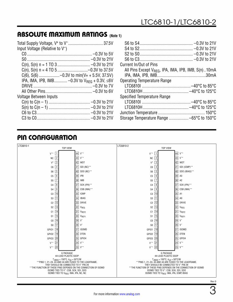
ABSOLUTE MAXIMUM RATINGS (Note 1)
Total Supply Voltage, V+ to V– ................................ 37.5VInput Voltage (Relative to V–)
C0 ............................................................ –0.3V to 5VS0 .......................................................... –0.3V to 21VC(n), S(n) n = 1 TO 3 .............................. –0.3V to 21VC(n), S(n) n = 4 TO 5 ............................–0.3V to 37.5V C(6), S(6) ...................–0.3V to min(V+ + 5.5V, 37.5V)IPA, IMA, IPB, IMB ............ –0.3V to VREG + 0.3V, ≤6VDRIVE ...................................................... –0.3V to 7VAll Other Pins ........................................... –0.3V to 6V
Voltage Between Inputs C(n) to C(n – 1) ...................................... –0.3V to 21VS(n) to C(n – 1) ...................................... –0.3V to 21VC6 to C3 ................................................. –0.3V to 21VC3 to C0 ................................................. –0.3V to 21V
PIN CONFIGURATIONLTC6810-1 LTC6810-2
1
2
3
4
5
6
7
8
9
10
11
12
13
14
15
16
17
18
19
20
21
22
TOP VIEW
G PACKAGE44-LEAD PLASTIC SSOP
TJMAX = 150°C, JA = 50°C/W**PINS 1, 21–24, 43 AND 44 ARE FUSED TO THE LEADFRAME.
THEY SHOULD BE CONNECTED TO V– PIN 29**THE FUNCTION OF THESE PINS DEPENDS ON THE CONNECTION OF ISOMD
ISOMD TIED TO V–: CSB, SCK, SDI, SDOISOMD TIED TO VREG: IMA, IPA, NC, NC
44
43
42
41
40
39
38
37
36
35
34
33
32
31
30
29
28
27
26
25
24
23
V–*
NC
V+
C6
S6
C5
S5
C4
S4
C3
S3
C2
S2
C1
S1
C0
S0
GPIO1
GPIO2
GPIO3
V–*
V–*
V–*
V–*
WDT
SDI (NC)**
SDO (NC)**
IPB
IMB
SCK (IPA)**
CSB (IMA)**
ICMP
IBIAS
DRIVE
VREG
VREF2
VREF1
V–
V–
ISOMD
DTEN
GPIO4
V–*
V–*
1
2
3
4
5
6
7
8
9
10
11
12
13
14
15
16
17
18
19
20
21
22
TOP VIEW
G PACKAGE44-LEAD PLASTIC SSOP
TJMAX = 150°C, JA = 50°C/W**PINS 1, 21–24, 43 AND 44 ARE FUSED TO THE LEADFRAME.
THEY SHOULD BE CONNECTED TO V– PIN 29**THE FUNCTION OF THESE PINS DEPENDS ON THE CONNECTION OF ISOMD
ISOMD TIED TO V–: CSB, SCK, SDI, SDOISOMD TIED TO VREG: IMA, IPA, ICMP, IBIAS
44
43
42
41
40
39
38
37
36
35
34
33
32
31
30
29
28
27
26
25
24
23
V–*
NC
V+
C6
S6
C5
S5
C4
S4
C3
S3
C2
S2
C1
S1
C0
S0
GPIO1
GPIO2
GPIO3
V–*
V–*
V–*
V–*
WDT
SDI (ICMP)**
SDO (IBIAS)**
A3
A2
SCK (IPA)**
CSB (IMA)**
A1
A0
DRIVE
VREG
VREF2
VREF1
V–
V–
ISOMD
DTEN
GPIO4
V–*
V–*
S6 to S4 ................................................. –0.3V to 21VS4 to S2 ................................................. –0.3V to 21VS2 to S0 ................................................. –0.3V to 21VS6 to C3 ................................................. –0.3V to 21V
Current In/Out of Pins All Pins Except VREG, IPA, IMA, IPB, IMB, S(n) ..10mAIPA, IMA, IPB, IMB .............................................30mA
Operating Temperature Range LTC6810I .............................................–40°C to 85°CLTC6810H .......................................... –40°C to 125°C
Specified Temperature Range LTC6810I .............................................–40°C to 85°CLTC6810H .......................................... –40°C to 125°C
Junction Temperature ........................................... 150°CStorage Temperature Range .................. –65°C to 150°C
LTC6810-1/LTC6810-2
4Rev 0
For more information www.analog.com
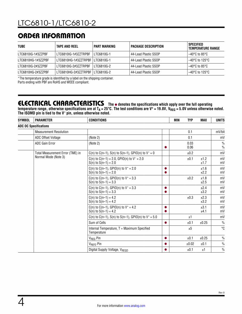
ORDER INFORMATIONTUBE TAPE AND REEL PART MARKING PACKAGE DESCRIPTION SPECIFIED
TEMPERATURE RANGE
LTC6810IG-1#3ZZPBF LTC6810IG-1#3ZZTRPBF LTC6810G-1 44-Lead Plastic SSOP –40°C to 85°C
LTC6810HG-1#3ZZPBF LTC6810HG-1#3ZZTRPBF LTC6810G-1 44-Lead Plastic SSOP –40°C to 125°C
LTC6810IG-2#3ZZPBF LTC6810IG-2#3ZZTRPBF LTC6810G-2 44-Lead Plastic SSOP –40°C to 85°C
LTC6810HG-2#3ZZPBF LTC6810HG-2#3ZZTRPBF LTC6810G-2 44-Lead Plastic SSOP –40°C to 125°C
*The temperature grade is identified by a label on the shipping container. Parts ending with PBF are RoHS and WEEE compliant.
ELECTRICAL CHARACTERISTICS
SYMBOL PARAMETER CONDITIONS MIN TYP MAX UNITS
ADC DC Specifications
Measurement Resolution 0.1 mV/bit
ADC Offset Voltage (Note 2) 0.1 mV
ADC Gain Error (Note 2)
l
0.03 0.06
% %
Total Measurement Error (TME) in Normal Mode (Note 3)
C(n) to C(n–1), S(n) to S(n–1), GPIO(n) to V– = 0 ±0.2 mV
C(n) to C(n–1) = 2.0, GPIO(n) to V– = 2.0 S(n) to S(n–1) = 2.0
±0.1 ±1.2 ±1.7
mV mV
C(n) to C(n–1), GPIO(n) to V– = 2.0 S(n) to S(n–1) = 2.0
l
l
±1.6 ±2.2
mV mV
C(n) to C(n–1), GPIO(n) to V– = 3.3 S(n) to S(n–1) = 3.3
±0.2 ±1.8 ±2.5
mV mV
C(n) to C(n–1), GPIO(n) to V– = 3.3 S(n) to S(n–1) = 3.3
l
l
±2.4 ±3.2
mV mV
C(n) to C(n–1) = 4.2 S(n) to S(n–1) = 4.2
±0.3 ±2.3 ±3.2
mV mV
C(n) to C(n–1), GPIO(n) to V– = 4.2 S(n) to S(n–1) = 4.2
l
l
±3.1 ±4.1
mV mV
C(n) to C(n–1), S(n) to S(n–1), GPIO(n) to V– = 5.0 ±1 mV
Sum of Cells l ±0.1 ±0.25 %
Internal Temperature, T = Maximum Specified Temperature
±5 °C
VREG Pin l ±0.1 ±0.25 %
VREF2 Pin l ±0.02 ±0.1 %
Digital Supply Voltage, VREGD l ±0.1 ±1 %
The l denotes the specifications which apply over the full operating temperature range, otherwise specifications are at TA = 25°C. The test conditions are V+ = 19.8V, VREG = 5.0V unless otherwise noted. The ISOMD pin is tied to the V– pin, unless otherwise noted.
LTC6810-1/LTC6810-2
5Rev 0
For more information www.analog.com
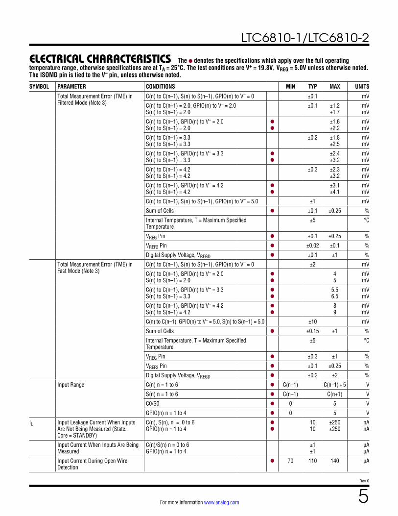
ELECTRICAL CHARACTERISTICS
SYMBOL PARAMETER CONDITIONS MIN TYP MAX UNITS
Total Measurement Error (TME) in Filtered Mode (Note 3)
C(n) to C(n–1), S(n) to S(n–1), GPIO(n) to V– = 0 ±0.1 mV
C(n) to C(n–1) = 2.0, GPIO(n) to V– = 2.0 S(n) to S(n–1) = 2.0
±0.1 ±1.2 ±1.7
mV mV
C(n) to C(n–1), GPIO(n) to V– = 2.0 S(n) to S(n–1) = 2.0
l
l
±1.6 ±2.2
mV mV
C(n) to C(n–1) = 3.3 S(n) to S(n–1) = 3.3
±0.2 ±1.8 ±2.5
mV mV
C(n) to C(n–1), GPIO(n) to V– = 3.3 S(n) to S(n–1) = 3.3
l
l
±2.4 ±3.2
mV mV
C(n) to C(n–1) = 4.2 S(n) to S(n–1) = 4.2
±0.3 ±2.3 ±3.2
mV mV
C(n) to C(n–1), GPIO(n) to V– = 4.2 S(n) to S(n–1) = 4.2
l
l
±3.1 ±4.1
mV mV
C(n) to C(n–1), S(n) to S(n–1), GPIO(n) to V– = 5.0 ±1 mV
Sum of Cells l ±0.1 ±0.25 %
Internal Temperature, T = Maximum Specified Temperature
±5 °C
VREG Pin l ±0.1 ±0.25 %
VREF2 Pin l ±0.02 ±0.1 %
Digital Supply Voltage, VREGD l ±0.1 ±1 %
Total Measurement Error (TME) in Fast Mode (Note 3)
C(n) to C(n–1), S(n) to S(n–1), GPIO(n) to V– = 0 ±2 mV
C(n) to C(n–1), GPIO(n) to V– = 2.0 S(n) to S(n–1) = 2.0
l
l
4 5
mV mV
C(n) to C(n–1), GPIO(n) to V– = 3.3 S(n) to S(n–1) = 3.3
l
l
5.5 6.5
mV mV
C(n) to C(n–1), GPIO(n) to V– = 4.2 S(n) to S(n–1) = 4.2
l
l
8 9
mV mV
C(n) to C(n–1), GPIO(n) to V– = 5.0, S(n) to S(n–1) = 5.0 ±10 mV
Sum of Cells l ±0.15 ±1 %
Internal Temperature, T = Maximum Specified Temperature
±5 °C
VREG Pin l ±0.3 ±1 %
VREF2 Pin l ±0.1 ±0.25 %
Digital Supply Voltage, VREGD l ±0.2 ±2 %
Input Range C(n) n = 1 to 6 l C(n–1) C(n–1) + 5 V
S(n) n = 1 to 6 l C(n–1) C(n+1) V
C0/S0 l 0 5 V
GPIO(n) n = 1 to 4 l 0 5 V
IL Input Leakage Current When Inputs Are Not Being Measured (State: Core = STANDBY)
C(n), S(n), n = 0 to 6 GPIO(n) n = 1 to 4
l
l
10 10
±250 ±250
nA nA
Input Current When Inputs Are Being Measured
C(n)/S(n) n = 0 to 6 GPIO(n) n = 1 to 4
±1 ±1
µA µA
Input Current During Open Wire Detection
l 70 110 140 µA
The l denotes the specifications which apply over the full operating temperature range, otherwise specifications are at TA = 25°C. The test conditions are V+ = 19.8V, VREG = 5.0V unless otherwise noted. The ISOMD pin is tied to the V– pin, unless otherwise noted.

LTC6810-1/LTC6810-2
6Rev 0
For more information www.analog.com
ELECTRICAL CHARACTERISTICS
SYMBOL PARAMETER CONDITIONS MIN TYP MAX UNITS
Voltage Reference Specifications
VREF1 1st Reference Voltage VREF1 Pin, No Load l 3.1 3.2 3.3 V
1st Reference Voltage TC VREF1 Pin, No Load 3 ppm/°C
1st Reference Voltage Hysteresis VREF1 Pin, No Load 20 ppm
1st Reference V. Long Term Drift VREF1 Pin, No Load 25 ppm/√khr
VREF2 2nd Reference Voltage VREF2 Pin, No Load l 2.995 3 3.005 V
VREF2 Pin, 5k Load to V– l 2.994 3 3.006 V
2nd Reference Voltage TC VREF2 Pin, No Load 10 ppm/°C
2nd Reference Voltage Hysteresis VREF2 Pin, No Load 100 ppm
2nd Reference V. Long Term Drift VREF2 Pin, No Load 60 ppm/√khr
General DC Specifications
IVP V+ Supply Current (See Figure 1: Operation State Diagram)
State: Core = SLEEP, isoSPI = IDLE VREG = 0V 5.7 10 µA
VREG = 0V l 5.7 15 µA
VREG = 5V 3.5 5.5 µA
VREG = 5V l 3.5 9 µA
State: Core = STANDBY Internal REG Disabled
l
14 10
22 35 45
µA µA
State: Core = REFUP
l
25 20
35 50 60
µA µA
State: Core = MEASURE
l
30 25
50 50
70 80
µA µA
IVP_INTREG Total V+ Current when Internal REG Enabled = IVP +IREG
State: Core = STANDBY Internal REG Enabled
l
70 60
130 175 200
µA µA
IREG(CORE) VREG Supply Current (See Figure 1: Operation State Diagram)
State: Core = SLEEP, isoSPI = IDLE VREG = 5V 3.5 6.5 µA
VREG = 5V l 3.5 9 µA
State: Core = STANDBY
l
20 18
48 75 85
µA µA
State: Core = REFUP
l
1.2 1.1
1.7 2.2 2.3
mA mA
State: Core = MEASURE
l
5.7 5.5
6.2 6.2
6.6 6.8
mA mA
IREG(isoSPI) Additional VREG Supply Current If isoSPI in READY/ACTIVE States Note: ACTIVE State Current Assumes tCLK = 1µs, (Note 3)
LTC6810-2: ISOMD = 1, RB1 + RB2 = 2k
READY l 3.6 4.5 5.4 mA
ACTIVE l 4.6 5.8 7.0 mA
LTC6810-1: ISOMD = 0, RB1 + RB2 = 2k
READY l 3.6 4.5 5.2 mA
ACTIVE l 5.6 6.8 8.1 mA
LTC6810-1: ISOMD = 1, RB1 + RB2 = 2k
READY l 4.0 5.2 6.5 mA
ACTIVE l 7.0 8.5 10.5 mA
LTC6810-2: ISOMD = 1, RB1 + RB2 = 20k
READY l 1.0 1.8 2.6 mA
ACTIVE l 1.2 2.2 3.2 mA
LTC6810-1: ISOMD = 0, RB1 + RB2 = 20k
READY l 1.0 1.8 2.6 mA
ACTIVE l 1.3 2.3 3.3 mA
LTC6810-1: ISOMD = 1, RB1 + RB2 = 20k
READY l 1.6 2.5 3.5 mA
ACTIVE l 1.8 3.1 4.8 mA
The l denotes the specifications which apply over the full operating temperature range, otherwise specifications are at TA = 25°C. The test conditions are V+ = 19.8V, VREG = 5.0V unless otherwise noted. The ISOMD pin is tied to the V– pin, unless otherwise noted.
LTC6810-1/LTC6810-2
7Rev 0
For more information www.analog.com
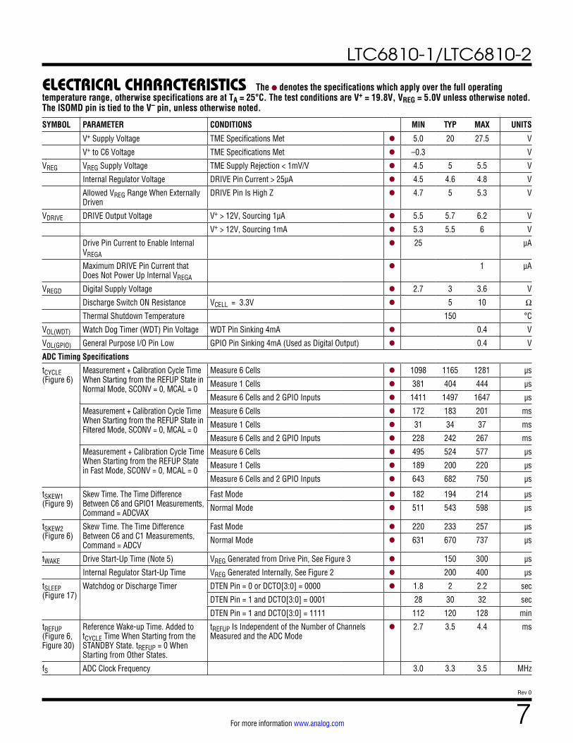
ELECTRICAL CHARACTERISTICS
SYMBOL PARAMETER CONDITIONS MIN TYP MAX UNITS
V+ Supply Voltage TME Specifications Met l 5.0 20 27.5 V
V+ to C6 Voltage TME Specifications Met l –0.3 V
VREG VREG Supply Voltage TME Supply Rejection < 1mV/V l 4.5 5 5.5 V
Internal Regulator Voltage DRIVE Pin Current > 25µA l 4.5 4.6 4.8 V
Allowed VREG Range When Externally Driven
DRIVE Pin Is High Z l 4.7 5 5.3 V
VDRIVE DRIVE Output Voltage V+ > 12V, Sourcing 1µA l 5.5 5.7 6.2 V
V+ > 12V, Sourcing 1mA l 5.3 5.5 6 V
Drive Pin Current to Enable Internal VREGA
l 25 µA
Maximum DRIVE Pin Current that Does Not Power Up Internal VREGA
l 1 µA
VREGD Digital Supply Voltage l 2.7 3 3.6 V
Discharge Switch ON Resistance VCELL = 3.3V l 5 10 Ω
Thermal Shutdown Temperature 150 °C
VOL(WDT) Watch Dog Timer (WDT) Pin Voltage WDT Pin Sinking 4mA l 0.4 V
VOL(GPIO) General Purpose I/O Pin Low GPIO Pin Sinking 4mA (Used as Digital Output) l 0.4 V
ADC Timing Specifications
tCYCLE (Figure 6)
Measurement + Calibration Cycle Time When Starting from the REFUP State in Normal Mode, SCONV = 0, MCAL = 0
Measure 6 Cells l 1098 1165 1281 µs
Measure 1 Cells l 381 404 444 µs
Measure 6 Cells and 2 GPIO Inputs l 1411 1497 1647 µs
Measurement + Calibration Cycle Time When Starting from the REFUP State in Filtered Mode, SCONV = 0, MCAL = 0
Measure 6 Cells l 172 183 201 ms
Measure 1 Cells l 31 34 37 ms
Measure 6 Cells and 2 GPIO Inputs l 228 242 267 ms
Measurement + Calibration Cycle Time When Starting from the REFUP State in Fast Mode, SCONV = 0, MCAL = 0
Measure 6 Cells l 495 524 577 µs
Measure 1 Cells l 189 200 220 µs
Measure 6 Cells and 2 GPIO Inputs l 643 682 750 µs
tSKEW1 (Figure 9)
Skew Time. The Time Difference Between C6 and GPIO1 Measurements, Command = ADCVAX
Fast Mode l 182 194 214 µs
Normal Mode l 511 543 598 µs
tSKEW2 (Figure 6)
Skew Time. The Time Difference Between C6 and C1 Measurements, Command = ADCV
Fast Mode l 220 233 257 µs
Normal Mode l 631 670 737 µs
tWAKE Drive Start-Up Time (Note 5) VREG Generated from Drive Pin, See Figure 3 l 150 300 µs
Internal Regulator Start-Up Time VREG Generated Internally, See Figure 2 l 200 400 µs
tSLEEP (Figure 17)
Watchdog or Discharge Timer DTEN Pin = 0 or DCTO[3:0] = 0000 l 1.8 2 2.2 sec
DTEN Pin = 1 and DCTO[3:0] = 0001 28 30 32 sec
DTEN Pin = 1 and DCTO[3:0] = 1111 112 120 128 min
tREFUP (Figure 6, Figure 30)
Reference Wake-up Time. Added to tCYCLE Time When Starting from the STANDBY State. tREFUP = 0 When Starting from Other States.
tREFUP Is Independent of the Number of Channels Measured and the ADC Mode
l 2.7 3.5 4.4 ms
fS ADC Clock Frequency 3.0 3.3 3.5 MHz
The l denotes the specifications which apply over the full operating temperature range, otherwise specifications are at TA = 25°C. The test conditions are V+ = 19.8V, VREG = 5.0V unless otherwise noted. The ISOMD pin is tied to the V– pin, unless otherwise noted.

LTC6810-1/LTC6810-2
8Rev 0
For more information www.analog.com
ELECTRICAL CHARACTERISTICS
SYMBOL PARAMETER CONDITIONS MIN TYP MAX UNITS
SPI Interface DC Specifications
VIH(SPI) SPI Pin Digital Input Voltage High Pins CSB, SCK, SDI l 2.3 V
VIL(SPI) SPI Pin Digital Input Voltage Low Pins CSB, SCK, SDI l 0.8 V
VIH(ADDR) Address Pin Digital Input Voltage High Pins ISOMD, DTEN, GPIO1 to GPIO4, A0–A3 l 2.7 V
VIL(ADDR) Address Pin Digital Input Voltage Low Pins ISOMD, DTEN, GPIO1 to GPIO4, A0–A3 l 1.2 V
ILEAK(DIG) Digital Input Current Pins CSB, SCK, SDI, ISOMD, DTEN, A0 to A3 l ±1 µA
VOL(SDO) Digital Output Low Pins SDO sinking 1mA l 0.3 V
isoSPI DC Specifications (see Figure 23)
VBIAS Voltage on IBIAS Pin READY/ACTIVE State IDLE State
l 1.9 2 0
2.1 V V
IB Isolated Interface Bias Current IB = VBIAS/(RB1 + RB2) l 0.1 1 mA
AIB Isolated Interface Current Gain VA ≤ 1.6V IB = 1mA l 18 20 22 mA/mA
IB = 0.1mA l 18 20 23 mA/mA
VA Transmitter Pulse Amplitude VA = |VIP – VIM| l 1.6 V
VICMP Threshold-Setting Voltage on ICMP Pin
VTCMP = ATCMP • VICMP l 0.2 1.5 V
ILEAK(ICMP) Input Leakage Current on ICMP Pin l ±1 µA
ILEAK(IP/IM) Leakage Current on IP and IM Pins IDLE State, VIP or VIM, 0V to VREG l ±1 µA
ATCMP Receiver Comparator Threshold Voltage Gain
VCM = 2.5V to VREG – 0.2 l 0.4 0.5 0.6 V/V
VIP/IM Receiver Voltage Range (Single-Ended)
l –0.3 VREG + 0.3 V
VCM Receiver Common-Mode Bias IP/IM Not Driving (VREG – VICMP/3 – 167mV) V
RIN Receiver Input Resistance Single-Ended to IPA, IMA, IPB, IMB l 26 35 45 kΩ
isoSPI Idle/Wake-up Specifications (see Figure 30)
VWAKE Differential Wake-up Voltage VWAKE = |VIPA – VIMA| l 250 mV
tDWELL Dwell Time at VWAKE Before Wake Detection
l 240 ns
tREADY Start-Up Time After Wake Detection l 10 µs
tIDLE Idle Timeout Duration l 4.3 5.5 6.7 ms
isoSPI Pulse Timing Specifications (see Figure 28)
t½PW(CS) Chip-Select Half-Pulse Width Transmitter l 120 150 180 ns
tFILT(CS) Chip-Select Signal Filter Receiver l 70 90 110 ns
tINV(CS) Chip-Select Pulse Inversion Delay Transmitter l 120 155 190 ns
tWNDW(CS) Chip-Select Valid Pulse Window Receiver l 220 270 330 ns
t½PW(D) Data Half-Pulse Width Transmitter l 40 50 60 ns
tFILT(D) Data Signal Filter Receiver l 10 25 35 ns
tINV(D) Data Pulse Inversion Delay Transmitter l 40 55 65 ns
tWNDW(D) Data Valid Pulse Window Receiver l 70 90 110 ns
The l denotes the specifications which apply over the full operating temperature range, otherwise specifications are at TA = 25°C. The test conditions are V+ = 19.8V, VREG = 5.0V unless otherwise noted. The ISOMD pin is tied to the V– pin, unless otherwise noted.

LTC6810-1/LTC6810-2
9Rev 0
For more information www.analog.com
Note 1: Stresses beyond those listed under Absolute Maximum Ratings may cause permanent damage to the device. Exposure to any Absolute Maximum Rating condition for extended periods may affect device reliability and lifetime.Note 2: The ADC specifications are guaranteed by the Total Measurement Error specification.Note 3: S pin TME may differ from C pin TME by several bits due to the quantization noise of the ADC and the different external filtering on the C and S pins.Note 4: The ACTIVE state current is calculated from DC measurements. The ACTIVE state current is the additional average supply current into VREG when there is continuous 1MHz communications on the isoSPI ports with 50% data 1s and 50% data 0s. Slower clock rates reduce the supply current. See Applications Information section for additional details.
ELECTRICAL CHARACTERISTICS
SYMBOL PARAMETER CONDITIONS MIN TYP MAX UNITS
SPI Timing Requirements (see Figure 22 and Figure 29)
tCLK SCK Period (Note 6) l 1 µs
t1 SDI Setup Time Before SCK Rising Edge
l 25 ns
t2 SDI Hold Time After SCK Rising Edge l 25 ns
t3 SCK Low tCLK = t3 + t4 ³ 1µs l 200 ns
t4 SCK High tCLK = t3 + t4 ³ 1µs l 200 ns
t5 CS Rising Edge to CS Falling Edge l 0.6 µs
t6 SCK Rising Edge to CS Rising Edge (Note 6) l 0.8 µs
t7 CS Falling Edge to SCK Rising Edge (Note 6) l 1 µs
isoSPI Timing Specifications (see Figure 29)
t8 SCK Falling Edge to SDO Valid (Note 7) l 60 ns
t9 SCK Rising Edge to Short ±1 Transmit l 50 ns
t10 CS Transition to Long ±1 Transmit l 60 ns
t11 CS Rising Edge to SDO Rising (Note 7) l 200 ns
tRTN Data Return Delay l 325 375 425 ns
tDSY(CS) Chip-Select Daisy-Chain Delay l 120 180 ns
tDSY(D) Data Daisy-Chain Delay l 200 250 300 ns
tLAG Data Daisy-Chain Lag (vs. Chip-Select) = [tDSY(D) + t½PW(D)] – [tDSY(CS) + t½PW(CS)] l 0 55 70 ns
t5(GOV) Chip-Select High-to-Low Pulse Governor
l 0.6 0.82 µs
t6(GOV) Data to Chip-Select Pulse Governor l 0.8 1.05 µs
tBLOCK isoSPI Port Reversal Blocking Window l 2 10 µs
The l denotes the specifications which apply over the full operating temperature range, otherwise specifications are at TA = 25°C. The test conditions are V+ = 19.8V, VREG = 5.0V unless otherwise noted. The ISOMD pin is tied to the V– pin, unless otherwise noted.
Note 5: VREG is generated from the Drive pin and an external NPN transistor, see Figure 3.Note 6: These timing specifications are dependent on the delay through the cable, and include allowances for 50ns of delay each direction. 50ns corresponds to 10m of CAT-5 cable (which has a velocity of propagation of 66% the speed of light). Use of longer cables would require derating these specs by the amount of additional delay.Note 7: These specifications do not include rise or fall time of SDO. While fall time (typically 5ns due to the internal pull-down transistor) is not a concern, rising-edge transition time tRISE is dependent on the pull-up resistance and load capacitance on the SDO pin. The time constant must be chosen such that SDO meets the setup time requirements of the MCU.

LTC6810-1/LTC6810-2
10Rev 0
For more information www.analog.com
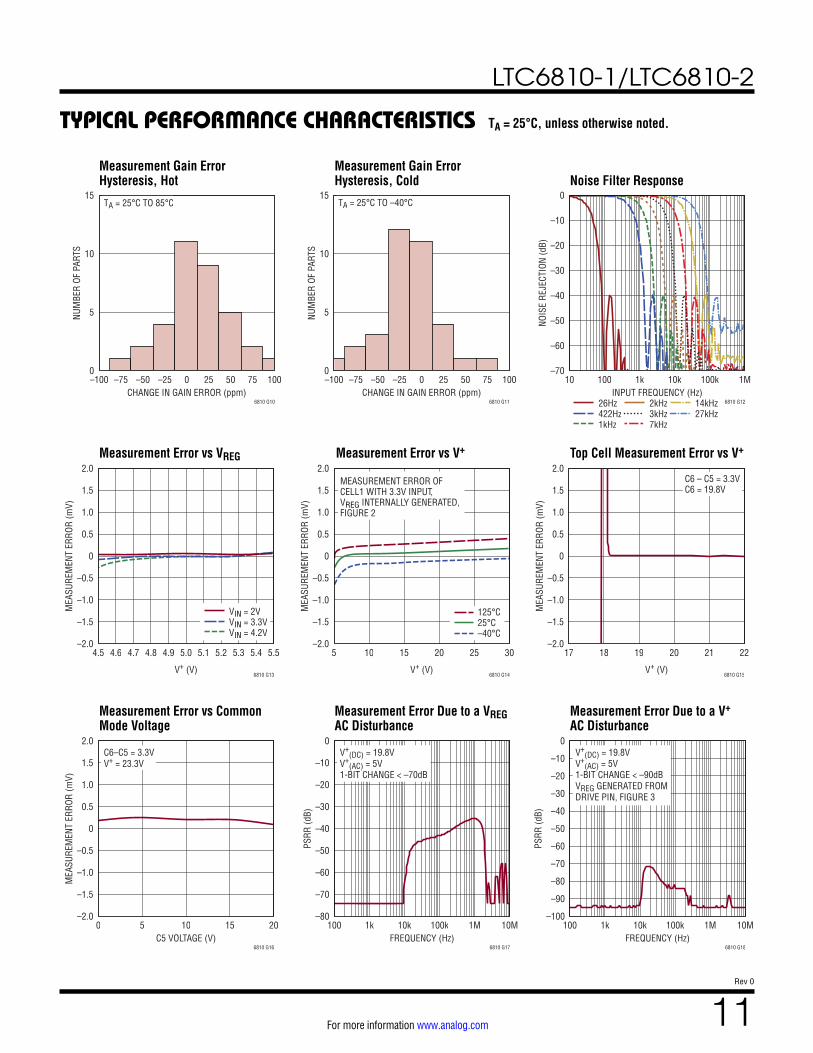
TYPICAL PERFORMANCE CHARACTERISTICS
Measurement Error vs Temperature
Measurement Error Due to IR Reflow
Measurement Error Long Term Drift
Measurement Error vs Input Normal Mode
Measurement Error vs Input Filtered Mode
Measurement Error vs Input Fast Mode
Measurement Noise vs Input Normal Mode
Measurement Noise vs Input Filtered Mode
Measurement Noise vs Input Fast Mode
TA = 25°C, unless otherwise noted.
CELL VOLTAGE = 3.3V5 TYPICAL UNITS
TEMPERATURE (°C)–50 –25 0 25 50 75 100 125
–2.0
–1.5
–1.0
–0.5
0
0.5
1.0
1.5
2.0
MEA
SURE
MEN
T ER
ROR
(mV)
6810 G01CHANGE IN GAIN ERROR (ppm)
–400 –300 –200 –100 0 1000
5
10
15
20
NUM
BER
OF P
ARTS
6810 G02TIME (HOURS)
0 500 1000 1500 2000 2500–30
–25
–20
–15
–10
–5
0
5
10
15
20
MEA
SURE
MEN
T ER
ROR
(ppm
)
6810 G03
10 ADC MEASUREMENTS AVERAGED AT EACH INPUT
INPUT (V)0 1 2 3 4 5
–2.0
–1.5
–1.0
–0.5
0
0.5
1.0
1.5
2.0
MEA
SURE
MEN
T ER
ROR
(mV)
6810 G04
10 ADC MEASUREMENTSAVERAGED AT EACH INPUT
INPUT (V)0 1 2 3 4 5
–2.0
–1.5
–1.0
–0.5
0
0.5
1.0
1.5
2.0
MEA
SURE
MEN
T ER
ROR
(mV)
6810 G05
10 ADC MEASUREMENTSAVERAGED AT EACH INPUT
INPUT (V)0 1 2 3 4 5
–10.0
–8.0
–6.0
–4.0
–2.0
0
2.0
4.0
6.0
8.0
10.0
MEA
SURE
MEN
T ER
ROR
(mV)
6810 G06
INPUT (V)0 1 2 3 4 5
0
0.1
0.2
0.3
0.4
0.5
0.6
0.7
0.8
0.9
1.0
PEAK
NOI
SE (m
V)
6810 G07INPUT (V)
0 1 2 3 4 50
0.1
0.2
0.3
0.4
0.5
0.6
0.7
0.8
0.9
1.0
PEAK
NOI
SE (m
V)
6810 G08INPUT (V)
0 1 2 3 4 50
1.0
2.0
3.0
4.0
5.0
6.0
7.0
8.0
9.0
10.0
PEAK
NOI
SE (m
V)
6810 G09
LTC6810-1/LTC6810-2
11Rev 0
For more information www.analog.com
TYPICAL PERFORMANCE CHARACTERISTICS
Measurement Gain Error Hysteresis, Hot
Measurement Gain Error Hysteresis, Cold Noise Filter Response
Measurement Error vs VREG Measurement Error vs V+ Top Cell Measurement Error vs V+
Measurement Error vs Common Mode Voltage
Measurement Error Due to a VREG AC Disturbance
Measurement Error Due to a V+ AC Disturbance
TA = 25°C, unless otherwise noted.
TA = 25°C TO 85°C
CHANGE IN GAIN ERROR (ppm)–100 –75 –50 –25 0 25 50 75 1000
5
10
15
NUM
BER
OF P
ARTS
6810 G10
TA = 25°C TO –40°C
CHANGE IN GAIN ERROR (ppm)–100 –75 –50 –25 0 25 50 75 1000
5
10
15
NUM
BER
OF P
ARTS
6810 G11 26Hz422Hz1kHz
2kHz3kHz7kHz
14kHz27kHz
INPUT FREQUENCY (Hz)10 100 1k 10k 100k 1M
–70
–60
–50
–40
–30
–20
–10
0
NOIS
E RE
JECT
ION
(dB)
6810 G12
V+ (V)
4.5 4.6 4.7 4.8 4.9 5.0 5.1 5.2 5.3 5.4 5.5–2.0
–1.5
–1.0
–0.5
0
0.5
1.0
1.5
2.0
MEA
SURE
MEN
T ER
ROR
(mV)
6810 G13
VIN = 2VVIN = 3.3VVIN = 4.2V
MEASUREMENT ERROR OFCELL1 WITH 3.3V INPUT,VREG INTERNALLY GENERATED,FIGURE 2
V+ (V)
5 10 15 20 25 30–2.0
–1.5
–1.0
–0.5
0
0.5
1.0
1.5
2.0
MEA
SURE
MEN
T ER
ROR
(mV)
125°C25°C–40°C
6810 G14
C6 – C5 = 3.3VC6 = 19.8V
V+ (V)
17 18 19 20 21 22–2.0
–1.5
–1.0
–0.5
0
0.5
1.0
1.5
2.0
MEA
SURE
MEN
T ER
ROR
(mV)
6810 G15
C5 VOLTAGE (V)0 5 10 15 20
–2.0
–1.5
–1.0
–0.5
0
0.5
1.0
1.5
2.0
MEA
SURE
MEN
T ER
ROR
(mV)
6810 G16
C6–C5 = 3.3VV+ = 23.3V
V+(DC) = 19.8V
V+(AC) = 5V
1-BIT CHANGE < –70dB
FREQUENCY (Hz)100 1k 10k 100k 1M 10M
–80
–70
–60
–50
–40
–30
–20
–10
0
PSRR
(dB)
6810 G17FREQUENCY (Hz)
100 1k 10k 100k 1M 10M–100
–90
–80
–70
–60
–50
–40
–30
–20
–10
0
PSRR
(dB)
6810 G18
V+(DC) = 19.8V
V+(AC) = 5V
1-BIT CHANGE < –90dBVREG GENERATED FROMDRIVE PIN, FIGURE 3
LTC6810-1/LTC6810-2
12Rev 0
For more information www.analog.com
TYPICAL PERFORMANCE CHARACTERISTICS
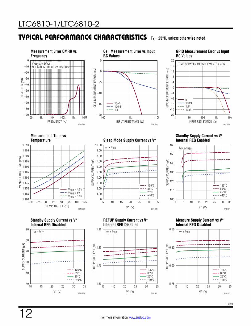
Measurement Error CMRR vs Frequency
Cell Measurement Error vs Input RC Values
GPIO Measurement Error vs Input RC Values
Measurement Time vs Temperature Sleep Mode Supply Current vs V+
Standby Supply Current vs V+ Internal REG Enabled
Standby Supply Current vs V+ Internal REG Disabled
REFUP Supply Current vs V+ Internal REG Disabled
Measure Supply Current vs V+
Internal REG Disabled
TA = 25°C, unless otherwise noted.
VCM(IN) = 5VP-PNORMAL MODE CONVERSIONS
FREQUENCY (Hz)100 1k 10k 100k 1M 10M
–90
–80
–70
–60
–50
–40
–30
–20
–10
0
REJE
CTIO
N (d
B)
6810 G19
10nF100nF1µF
INPUT RESISTANCE (Ω)100 1k 10k
–20
–15
–10
–5
0
5
CELL
MEA
SURM
ENT
ERRO
R (m
V)
6810 G20
TIME BETWEEN MEASUREMENTS > 3RC
0100nF1µF10µF
INPUT RESISTANCE (Ω)1 10 100 1k 10k
–20
–16
–12
–8
–4
0
4
8
12
16
20
GPIO
MEA
SURM
ENT
ERRO
R (m
V)
6810 G21
VREG = 4.5VVREG = 5VVREG = 5.5V
TEMPERATURE (°C)–50 –25 0 25 50 75 100 125
1.160
1.165
1.170
1.175
1.180
1.185
1.190
1.195
1.200
1.205
1.210
MEA
SURE
MEN
T TI
ME
(mS)
6810 G22
IVP + IREG
V+ (V)
5 10 15 20 25 30 350
1.00
2.00
3.00
4.00
5.00
6.00
7.00
8.00
9.00
10.00
SUPP
LY C
URRE
NT (µ
A)
6810 G23
125°C85°C25°C–40°C
IVP_INTREG
V+ (V)
0 5 10 15 20 25 30 35100
110
120
130
140
150
160
SUPP
LY C
URRE
NT (µ
A)
6810 G24
125°C85°C25°C–40°C
IVP + IREG
V+ (V)
10 15 20 25 30 3540
50
60
70
80
90
SUPP
LY C
URRE
NT (µ
A)
6810 G25
125°C85°C25°C–40°C
IVP + IREG
V+ (V)
10 15 20 25 30 351.60
1.70
1.80
1.90
SUPP
LY C
URRE
NT (m
A)
6810 G26
125°C85°C25°C–40°C
IVP + IREG
V+ (V)
10 15 20 25 30 355.75
6.00
6.25
6.50
SUPP
LY C
URRE
NT (m
A)
6810 G27
125°C85°C25°C–40°C
LTC6810-1/LTC6810-2
13Rev 0
For more information www.analog.com
TYPICAL PERFORMANCE CHARACTERISTICS
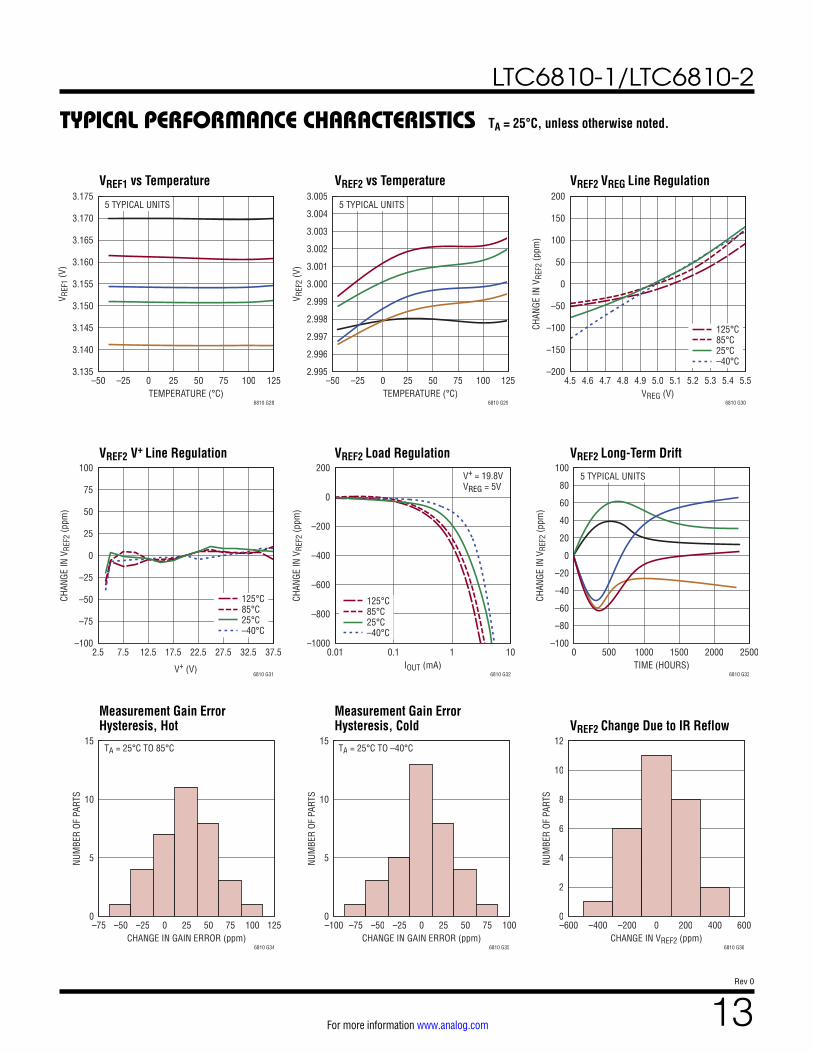
VREF1 vs Temperature VREF2 vs Temperature VREF2 VREG Line Regulation
VREF2 V+ Line Regulation VREF2 Load Regulation VREF2 Long-Term Drift
Measurement Gain Error Hysteresis, Hot
Measurement Gain Error Hysteresis, Cold VREF2 Change Due to IR Reflow
TA = 25°C, unless otherwise noted.
5 TYPICAL UNITS
TEMPERATURE (°C)–50 –25 0 25 50 75 100 125
3.135
3.140
3.145
3.150
3.155
3.160
3.165
3.170
3.175
V REF
1 (V
)
6810 G28
5 TYPICAL UNITS
TEMPERATURE (°C)–50 –25 0 25 50 75 100 125
2.995
2.996
2.997
2.998
2.999
3.000
3.001
3.002
3.003
3.004
3.005
V REF
2 (V
)
6810 G29VREG (V)
4.5 4.6 4.7 4.8 4.9 5.0 5.1 5.2 5.3 5.4 5.5–200
–150
–100
–50
0
50
100
150
200
CHAN
GE IN
VRE
F2 (p
pm)
6810 G30
125°C85°C25°C–40°C
V+ (V)
2.5 7.5 12.5 17.5 22.5 27.5 32.5 37.5–100
–75
–50
–25
0
25
50
75
100
CHAN
GE IN
VRE
F2 (p
pm)
6810 G31
125°C85°C25°C–40°C
IOUT (mA)0.01 0.1 1 10
–1000
–800
–600
–400
–200
0
200
CHAN
GE IN
VRE
F2 (p
pm)
6810 G32
V+ = 19.8VVREG = 5V
125°C85°C25°C–40°C
TIME (HOURS)0 500 1000 1500 2000 2500
–100
–80
–60
–40
–20
0
20
40
60
80
100
CHAN
GE IN
VRE
F2 (p
pm)
6810 G33
5 TYPICAL UNITS
TA = 25°C TO 85°C
CHANGE IN GAIN ERROR (ppm)–75 –50 –25 0 25 50 75 100 125
0
5
10
15
NUM
BER
OF P
ARTS
6810 G34
TA = 25°C TO –40°C
CHANGE IN GAIN ERROR (ppm)–100 –75 –50 –25 0 25 50 75 1000
5
10
15
NUM
BER
OF P
ARTS
6810 G35CHANGE IN VREF2 (ppm)
–600 –400 –200 0 200 400 6000
2
4
6
8
10
12
NUM
BER
OF P
ARTS
6810 G36

LTC6810-1/LTC6810-2
14Rev 0
For more information www.analog.com
TYPICAL PERFORMANCE CHARACTERISTICS
VDRIVE vs Temperature VDRIVE V+ Line Regulation VDRIVE Load Regulation
Internal VREG Load Regulation Internal VREG Load RegulationVREG Pin Voltage vs V+ Pin Voltage
Discharge Switch On-Resistance vs Cell Voltage
Internal Die Temperature Increase vs Discharge Current
Internal Die Temperature Measurement Error vs Temperature
TA = 25°C, unless otherwise noted.
3 PARTS NO LOAD, 1mA LOAD
TEMPERATURE (oC)–50 –25 0 25 50 75 100 125
5.50
5.60
5.70
5.80
5.90
6.00
6.10
V DRI
VE (V
)
6810 G37V+ (V)
5 10 15 20 25 30 35–20
–15
–10
–5
0
5
10
15
20
CHAN
GE IN
VDR
IVE
(mm
V)
6810 G38
125°C85°C25°C–40°C
DRIVE PIN LOAD CURRENT (mA)0.01 0.1 1
–100
–90
–80
–70
–60
–50
–40
–30
–20
–10
0
CHAN
GE IN
VDR
IVE
(mV)
6810 G39
125°C85°C25°C–40°C
IOUT (mA)0 5 10 15 20 25 30
–300
–200
–100
0
CHAN
GE IN
VRE
G (m
V)
6810 G40
V+ = 10VINTERNAL LDO, FIGURE 2
125°C85°C25°C–40°C
NPN DISCONNECTED FROM VREGLOAD CURRENT INCLUDES IVREG OF THE CHIP
V+ below 10VV+=15VV+ above 20V
VREG LOAD CURRENT (mA)0 5 10 15 20 25 30
4.50
4.55
4.60
4.65
4.70
4.75
4.80
4.85
4.90
4.95
5.00
V REG
PIN
VOL
TAGE
(V)
6810 G41
NPN CONNECTED TO VREGVREG LOAD CURRENT = 25mA (INCLUDES IVREG)
TRANSITION BETWEEN INTERNAL LDOAND EXTERNAL NPN POWERED VREG
V+ PIN VOLTAGE (V)
5 10 15 20 25 304.50
4.60
4.70
4.80
4.90
5.00
5.10
5.20
5.30
5.40
5.50
V REG
PIN
VOL
TAGE
(V)
6810 G42
ON–RESISTANCE OF INTERNALDISCHARGE SWITCH MEASUREDBETWEEN S(n) AND S(n–1)
CELL VOLTAGE (V)1 1.5 2 2.5 3 3.5 4 4.5
2.0
3.0
4.0
5.0
6.0
7.0
8.0
9.0
10.0
DISC
HARG
E SW
ITCH
ON-
RESI
STAN
CE (Ω
)
6810 G43
125°C85°C25°C–40°C
1 CELL , 100%3 CELL, 100%6 CELL, 50%
INTERNAL DISCHARGE CURRENT (mA/CELL)0 50 100 150 200
0
5
10
15
20
25
30
35
40
INCR
EASE
IN T
EMPE
RATU
RE (°
C)
6810 G44
5 TYPICAL UNITS
TEMPERATURE (°C)–50 –25 0 25 50 75 100 125
–10
–8
–6
–4
–2
0
2
4
6
8
10
TEM
PERA
TURE
MEA
SURE
MEN
T ER
ROR
(°C)
6810 G46

LTC6810-1/LTC6810-2
15Rev 0
For more information www.analog.com
TYPICAL PERFORMANCE CHARACTERISTICS
VREF1 and VREF2 Power-Up VREG and VDRIVE Power-UpisoSPI Current (READY) vs Temperature
isoSPI Current (ACTIVE) vs isoSPI Clock Frequency IBIAS Voltage vs Temperature IBIAS Voltage Load Regulation
isoSPI Driver Current Gain (Port A/Port B) vs IBIAS Current
isoSPI Driver Current Gain (Port A/Port B) vs Temperature
TA = 25°C, unless otherwise noted.
VREF1
VREF2
500µs/DIV
CS5V/DIV
VREF11A/DIV
VREF21V/DIV
6810 G46
VREF1: CL = 1µFVREF2: CL = 1µF; RL = 5k
VREG GENERATED FROM DRIVE PINVREG: CL = 1µF
VDRIVE
VREG
50µs/DIV
CS5C/DIV
VREG2V/DIV
VDRIVE2A/DIV
6810 G47
IB = 1mA
LTC6813–1, ISOMD = V–
LTC6813–1, ISOMD = VREG
TEMPERATURE (°C)–50 –25 0 25 50 75 100 125
3.5
4.0
4.5
5.0
5.5
6.0
ISOS
PI C
URRE
NT (m
A)
6810 G48
ISOMD = VREGIB = 1mA
ISOSPI CLOCK FREQUENCY (kHz)0 200 400 600 800 1000
2
3
4
5
6
7
8
9
10
ISOS
PI C
URRE
NT
6810 G49
LTC6810-1, WRITELTC6810-1, READLTC6810-2, WRITELTC6810-2, READ
IB = 1mA3 PARTS
TEMPERATURE (°C)–50 –25 0 25 50 75 100 125
1.98
1.99
2.00
2.01
2.02
IBIA
S PI
N VO
LTAG
E (V
)
6810 G50IBIAS CURRENT, IB (µA)
0 200 400 600 800 10001.990
1.995
2.000
2.005
2.010
IBIA
S PI
N VO
LTAG
E (V
)
6810 G51
IBIAS CURRENT, IB (µA)0 200 400 600 800 1000
18
19
20
21
22
23
CURR
ENT
GAIN
, AIB
(m
A)
6810 G52
VA = 0.5VVA = 1VVA = 1.6V
TEMPERATURE (°C)–50 –25 0 25 50 75 100 125
18
19
20
21
22
23
CURR
ENT
GAIN
, AIB
(mA/
mA)
6810 G53
IB = 1mAIB = 100µA
LTC6810-1/LTC6810-2
16Rev 0
For more information www.analog.com
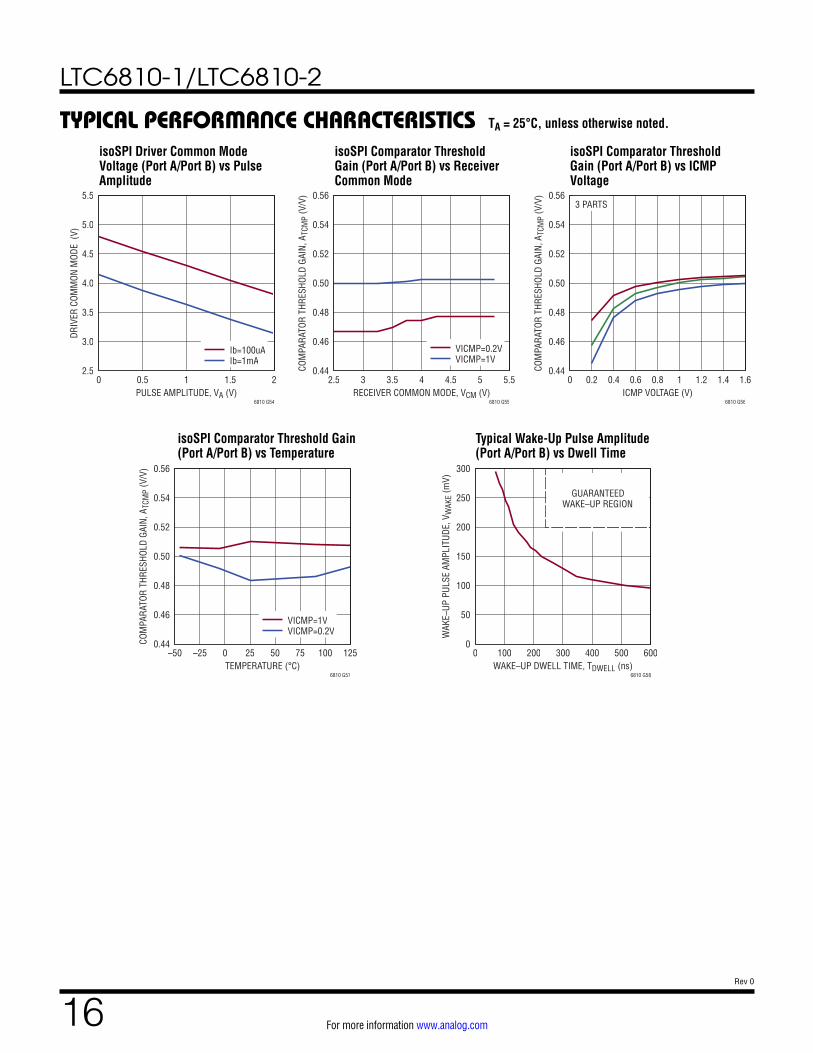
TYPICAL PERFORMANCE CHARACTERISTICSisoSPI Driver Common Mode Voltage (Port A/Port B) vs Pulse Amplitude
isoSPI Comparator Threshold Gain (Port A/Port B) vs Receiver Common Mode
isoSPI Comparator Threshold Gain (Port A/Port B) vs ICMP Voltage
isoSPI Comparator Threshold Gain (Port A/Port B) vs Temperature
Typical Wake-Up Pulse Amplitude (Port A/Port B) vs Dwell Time
TA = 25°C, unless otherwise noted.
Ib=100uAIb=1mA
PULSE AMPLITUDE, VA (V)0 0.5 1 1.5 2
2.5
3.0
3.5
4.0
4.5
5.0
5.5
DRIV
ER C
OMM
ON M
ODE
(V)
6810 G54
VICMP=0.2VVICMP=1V
RECEIVER COMMON MODE, VCM (V)2.5 3 3.5 4 4.5 5 5.5
0.44
0.46
0.48
0.50
0.52
0.54
0.56
COM
PARA
TOR
THRE
SHOL
D GA
IN, A
TCM
P (V
/V)
6810 G55
3 PARTS
ICMP VOLTAGE (V)0 0.2 0.4 0.6 0.8 1 1.2 1.4 1.6
0.44
0.46
0.48
0.50
0.52
0.54
0.56
COM
PARA
TOR
THRE
SHOL
D GA
IN, A
TCM
P (V
/V)
6810 G56
VICMP=1VVICMP=0.2V
TEMPERATURE (°C)–50 –25 0 25 50 75 100 125
0.44
0.46
0.48
0.50
0.52
0.54
0.56
COM
PARA
TOR
THRE
SHOL
D GA
IN, A
TCM
P (V
/V)
6810 G57
GUARANTEED WAKE–UP REGION
WAKE–UP DWELL TIME, TDWELL (ns)0 100 200 300 400 500 600
0
50
100
150
200
250
300
WAK
E–UP
PUL
SE A
MPL
ITUD
E, V
WAK
E (m
V)
6810 G58
LTC6810-1/LTC6810-2
17Rev 0
For more information www.analog.com
PIN FUNCTIONSC0 – C6: Cell Inputs.
S0 – S6: Balance Inputs/Outputs Redundant Cell Measurement. 6 NMOSFETs are connected between S(n) and S(n–1) for discharging cells. Additionally S pins can be used for redundant cell measurement.
V+: Positive Supply Pin.
V–: Negative Supply Pins. The V– pins must be shorted together, external to the IC.
V–*: These pins are fused to the leadframe, connect to V–.
VREF2: Buffered 2nd reference voltage for driving thermis-tors. Bypass with an external 1µF capacitor.
VREF1: ADC Reference Voltage. Bypass with an external 1µF capacitor. No DC loads allowed.
GPIO[1:4]: General Purpose I/O. Can be used as digital inputs or digital outputs, or as analog inputs with a mea-surement range from V– to 5V. GPIO[2:4] can be used as an I2C or SPI port.
DTEN: Discharge Timer Enable. Connect this pin to VREGto enable the Discharge Timer.
DRIVE: Connect the base of an NPN to this pin. Connect the collector to V+ and the emitter to VREG.
VREG: 5V Regulator Input. Bypass with an external 1μF capacitor.
ISOMD: Serial Interface Mode. Connecting ISOMD to VREG configures the LTC6810 for 2-wire isolated interface (isoSPI) mode. Connecting ISOMD to V– configures the LTC6810 for 4-wire SPI mode.
WDT: Watchdog Timer Output Pin. This is an open drain NMOS digital output. It can be left unconnected, or con-nected with a 1M resistor to VREG. If the LTC6810 does not receive a valid command within 2 seconds, the watch-dog timer circuit will reset the LTC6810 and the WDT pin will go high impedance.
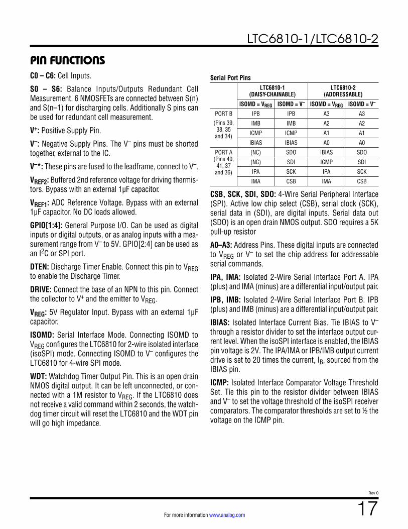
Serial Port PinsLTC6810-1
(DAISY-CHAINABLE)LTC6810-2
(ADDRESSABLE)
ISOMD = VREG ISOMD = V– ISOMD = VREG ISOMD = V–
PORT B(Pins 39,
38, 35 and 34)
IPB IPB A3 A3
IMB IMB A2 A2
ICMP ICMP A1 A1
IBIAS IBIAS A0 A0
PORT A (Pins 40,
41, 37 and 36)
(NC) SDO IBIAS SDO
(NC) SDI ICMP SDI
IPA SCK IPA SCK
IMA CSB IMA CSB
CSB, SCK, SDI, SDO: 4-Wire Serial Peripheral Interface (SPI). Active low chip select (CSB), serial clock (SCK), serial data in (SDI), are digital inputs. Serial data out (SDO) is an open drain NMOS output. SDO requires a 5K pull-up resistor
A0–A3: Address Pins. These digital inputs are connected to VREG or V– to set the chip address for addressable serial commands.
IPA, IMA: Isolated 2-Wire Serial Interface Port A. IPA (plus) and IMA (minus) are a differential input/output pair.
IPB, IMB: Isolated 2-Wire Serial Interface Port B. IPB (plus) and IMB (minus) are a differential input/output pair.
IBIAS: Isolated Interface Current Bias. Tie IBIAS to V– through a resistor divider to set the interface output cur-rent level. When the isoSPI interface is enabled, the IBIAS pin voltage is 2V. The IPA/IMA or IPB/IMB output current drive is set to 20 times the current, IB, sourced from the IBIAS pin.
ICMP: Isolated Interface Comparator Voltage Threshold Set. Tie this pin to the resistor divider between IBIAS and V– to set the voltage threshold of the isoSPI receiver comparators. The comparator thresholds are set to ½ the voltage on the ICMP pin.
LTC6810-1/LTC6810-2
18Rev 0
For more information www.analog.com
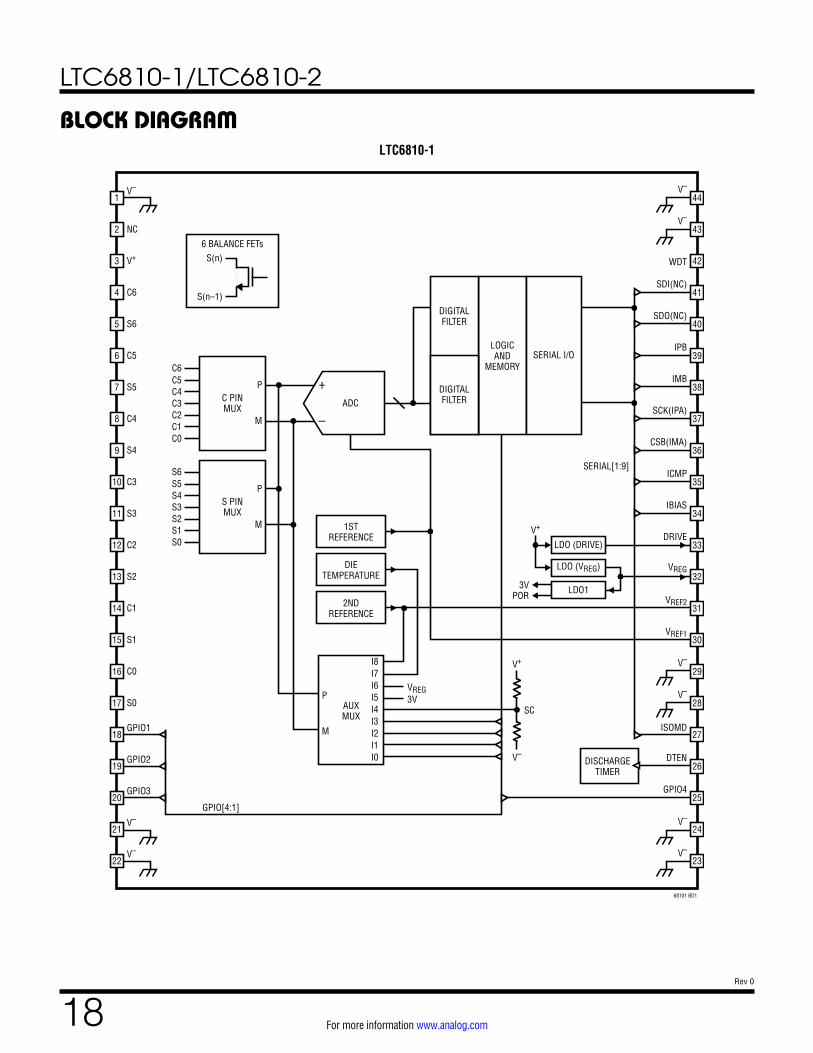
BLOCK DIAGRAM
3VPOR
VREG3V
I8I7I6I5I4I3I2I1I0
C0
C5C6
C4C3C2C1
68101 BD1
V–
V–
WDT
SDI(NC)
SDO(NC)
IPB
IMB
SCK(IPA)
CSB(IMA)
ICMP
IBIAS
DRIVE
VREG
VREF2
VREF1
V–
V–
ISOMD
DTEN
GPIO4
V–
V–
V–
NC
V+
C6
S6
C5
S5
C4
S4
C3
S3
C2
S2
C1
S1
C0
S0
GPIO1
GPIO2
GPIO[4:1]
SERIAL[1:9]
GPIO3
V–
V–
LOGICAND
MEMORY
DIGITALFILTER
DIGITALFILTER
SERIAL I/O
P
M
AUXMUX
6 BALANCE FETsS(n)
S(n–1)
P
M
C PINMUX
DIETEMPERATURE
2NDREFERENCE
1STREFERENCE
–
+ADC
S0
S5S6
S4S3S2S1
P
M
S PINMUX
LDO (DRIVE)
LDO (VREG)
LDO1
44
43
42
41
40
39
38
37
36
35
34
33
32
31
30
29
28
27
26
25
1
2
3
4
5
6
7
8
9
10
11
12
13
14
15
16
17
18
19
20
21
22
24
23
V+
V+
V–
SC
DISCHARGETIMER
LTC6810-1
LTC6810-1/LTC6810-2
19Rev 0
For more information www.analog.com
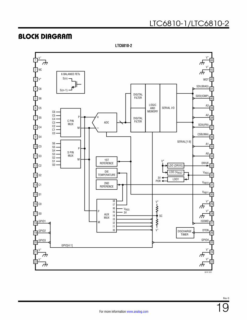
BLOCK DIAGRAM
3VPOR
VREG3V
I8I7I6I5I4I3I2I1I0
C0
C5C6
C4C3C2C1
68101 BD2
V–
V–
WDT
SDI(IBIAS)
SDO(ICMP)
A3
A2
SCK(IPA)
CSB(IMA)
A1
A0
DRIVE
VREG
VREF2
VREF1
V–
V–
ISOMD
DTEN
GPIO4
V–
V–
V–
NC
V+
C6
S6
C5
S5
C4
S4
C3
S3
C2
S2
C1
S1
C0
S0
GPIO1
GPIO2
GPIO[4:1]
SERIAL[1:9]
GPIO3
V–
V–
LOGICAND
MEMORY
DIGITALFILTER
DIGITALFILTER
P
M
AUXMUX
6 BALANCE FETsS(n)
S(n–1)
P
M
DISCHARGETIMER
DIETEMPERATURE
2NDREFERENCE
1STREFERENCE
–
+ADC
S0
S5S6
S4S3S2S1
P
M
LDO (DRIVE)
LDO (VREG)
LDO1
44
43
42
41
40
39
38
37
36
35
34
33
32
31
30
29
28
27
26
25
1
2
3
4
5
6
7
8
9
10
11
12
13
14
15
16
17
18
19
20
21
22
24
23
V+
V+
V–
SC
SERIAL I/O
C PINMUX
S PINMUX
LTC6810-2
LTC6810-1/LTC6810-2
20Rev 0
For more information www.analog.com
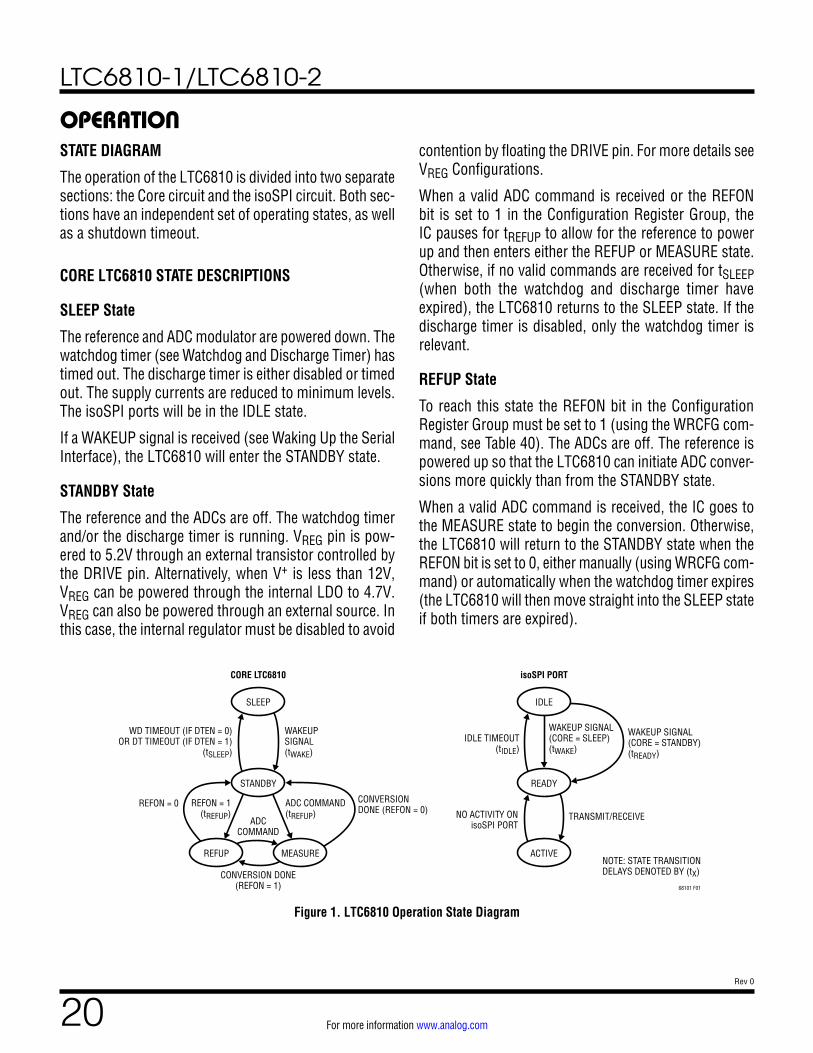
OPERATION
Figure 1. LTC6810 Operation State Diagram
68101 F01
isoSPI PORTCORE LTC6810
CONVERSION DONE(REFON = 1)
WAKEUPSIGNAL(tWAKE)
ADC COMMAND(tREFUP)
ADCCOMMAND
REFON = 1(tREFUP)
WAKEUP SIGNAL(CORE = STANDBY)(tREADY)
WAKEUP SIGNAL(CORE = SLEEP)(tWAKE)
TRANSMIT/RECEIVE
NOTE: STATE TRANSITIONDELAYS DENOTED BY (tX)
NO ACTIVITY ONisoSPI PORT
IDLE TIMEOUT(tIDLE)
CONVERSIONDONE (REFON = 0)
REFON = 0
WD TIMEOUT (IF DTEN = 0)OR DT TIMEOUT (IF DTEN = 1)
(tSLEEP)
MEASUREREFUP
STANDBY
SLEEP
ACTIVE
READY
IDLE
STATE DIAGRAM
The operation of the LTC6810 is divided into two separate sections: the Core circuit and the isoSPI circuit. Both sec-tions have an independent set of operating states, as well as a shutdown timeout.
CORE LTC6810 STATE DESCRIPTIONS
SLEEP State
The reference and ADC modulator are powered down. The watchdog timer (see Watchdog and Discharge Timer) has timed out. The discharge timer is either disabled or timed out. The supply currents are reduced to minimum levels. The isoSPI ports will be in the IDLE state.
If a WAKEUP signal is received (see Waking Up the Serial Interface), the LTC6810 will enter the STANDBY state.
STANDBY State
The reference and the ADCs are off. The watchdog timer and/or the discharge timer is running. VREG pin is pow-ered to 5.2V through an external transistor controlled by the DRIVE pin. Alternatively, when V+ is less than 12V, VREG can be powered through the internal LDO to 4.7V. VREG can also be powered through an external source. In this case, the internal regulator must be disabled to avoid
contention by floating the DRIVE pin. For more details see VREG Configurations.
When a valid ADC command is received or the REFON bit is set to 1 in the Configuration Register Group, the IC pauses for tREFUP to allow for the reference to power up and then enters either the REFUP or MEASURE state. Otherwise, if no valid commands are received for tSLEEP(when both the watchdog and discharge timer have expired), the LTC6810 returns to the SLEEP state. If the discharge timer is disabled, only the watchdog timer is relevant.
REFUP State
To reach this state the REFON bit in the Configuration Register Group must be set to 1 (using the WRCFG com-mand, see Table 40). The ADCs are off. The reference is powered up so that the LTC6810 can initiate ADC conver-sions more quickly than from the STANDBY state.
When a valid ADC command is received, the IC goes to the MEASURE state to begin the conversion. Otherwise, the LTC6810 will return to the STANDBY state when the REFON bit is set to 0, either manually (using WRCFG com-mand) or automatically when the watchdog timer expires (the LTC6810 will then move straight into the SLEEP state if both timers are expired).

LTC6810-1/LTC6810-2
21Rev 0
For more information www.analog.com
OPERATIONMEASURE State
The LTC6810 performs ADC conversions in this state. The reference and ADCs are powered up.
After ADC conversions are complete the LTC6810 will transition to either the REFUP or STANDBY states, depending on the REFON bit. Additional ADC conversions can be initiated more quickly by setting REFON = 1 to take advantage of the REFUP state.
Note: Non-ADC commands do not cause a Core state tran-sition. Only an ADC Conversion or DIAGN command will place the Core in the MEASURE state.
isoSPI STATE DESCRIPTIONS
Note: The LTC6810-1 has two isoSPI ports (A and B), for daisy-chain communication. The LTC6810-2 has only one isoSPI port (A), for parallel-addressable communication.
IDLE State
The isoSPI ports are powered down.
When isoSPI port A or port B (LTC6810-1 only) receives a WAKEUP signal (see Waking up the Serial Interface), the isoSPI enters the READY state. This transition happens quickly (within tREADY) if the Core is in the STANDBY state. If the Core is in the SLEEP state when the isoSPI receives a WAKEUP signal, the it transitions to the READY state within tWAKE.
READY State
The isoSPI port(s) are ready for communication. Port B is enabled only for LTC6810-1, and is not present on the LTC6810-2. The serial interface current in this state depends on if the part is LTC6810-1 or LTC6810-2, the status of the ISOMD pin, and RBIAS = RB1 + RB2 (the external resistors tied to the IBIAS pin).
If there is no activity (i.e. no WAKEUP signal) for greater than tIDLE = 5.5ms, the LTC6810 goes to the IDLE state. When the serial interface is transmitting or receiving data the LTC6810 goes to the ACTIVE state.
ACTIVE State
The LTC6810 is transmitting/receiving data using one or both of the isoSPI ports. The serial interface con-sumes maximum power in this state. The supply current increases with clock frequency as the density of isoSPI pulses increases.
POWER CONSUMPTION
The LTC6810 is powered via two pins: V+ and VREG. The V+ input requires voltage greater than or equal to the top cell voltage minus 0.3V, and it provides power to the high voltage elements of the core circuitry. The VREG input requires 5V and provides power to the remaining core circuitry and the isoSPI circuitry.
The power consumption varies according to the opera-tional states. The VREG input can be powered through an external transistor that is driven by the regulated DRIVE output pin, through the internal LDO, or through an exter-nal supply. The internal LDO is powered from V+, so in this configuration VREG current also comes from V+. Total V+ current when using the internal LDO to power VREG is given by,
IVP_INTREG = IVP + IREG
IVP current depends only on the Core state. However, IREGcurrent depends on both the Core state and isoSPI state, and can therefore be divided into two components. The isoSPI interface draws current only from the VREG pin.
IREG = IREG(Core) + IREG(isoSPI)
Table 1 provides typical values for IVP and IREG(Core) sup-ply currents in each of the Core states. Table 2 provides equations to approximate IREG(isoSPI) supply pin currents in each of the isoSPI states.
Table 1. Core Supply CurrentSTATE IVP IREG(CORE)
SLEEPVREG = 0V 5.7µA 0µA
VREG = 5V 3.5µA 3.3µA
STANDBY, Int Regulator Enabled 75µA 55µA
STANDBY, Int Regulator Disabled 20µA 55µA
REFUP 30µA 1.7mA
MEASURE 50µA 6.1mA

LTC6810-1/LTC6810-2
22Rev 0
For more information www.analog.com
OPERATIONTable 2. isoSPI Supply Current Equations
isoSPI STATE
ISOMD CONNECTION IREG(isoSPI)
IDLE N/A 0mAREADY VREG 2.2mA + 3 • IB
V– 1.5mA + 3 • IBACTIVE VREG
Write: 2.5mA 3 20 •100nstCLK
• IB
Read: 2.5mA 3 20 •100ns • 1.5
tCLK• IB
V–
1.8mA 3 20 •
100nstCLK
• IB
VREG CONFIGURATIONS
This section describes the different configurations that can be used to power VREG on the LTC6810. When V+
pin voltage is less than 12V, the DRIVE pin voltage drops below its nominal value as the regulator on the DRIVE pin does not have sufficient headroom. Under these condi-tions VREG pin cannot be powered through an external transistor. To overcome this problem, LTC6810 has an internal LDO that powers the VREG pin to 4.7V typically. The internal LDO can operate for V+ pin voltage as low as 5V. The internal LDO is enabled by applying a load current greater than 15µA on the DRIVE pin. Figure 2 shows a typical configuration for LTC6810 using the internal LDO when V+ is less than 12V. The suggested 100K resistor on the DRIVE pin draws a minimum of 30µA from the DRIVE pin. This keeps the internal regulator enabled.
Figure 2.
1µF100k
68101 F02
V+
DRIVE
VREG
V–
3V TO 5.8V
4.7V
5V TO 12VLTC6810
VREG Powered by Internal LDO
The power dissipation across the pass transistor in the internal LDO is (V+ – VREG ) • IREG. To limit the power dissipation inside the part it is recommended to power VREG using an external transistor when V+ pin voltage is greater than 12V. The external transistor is driven by the regulated DRIVE pin voltage that sets VREG pin voltage to 5.2V typically. The internal LDO is designed to only source current, so when VREG pin is driven to 5.2V by the external transistor the internal regulator is gracefully shutdown. Figure 3 shows a typical configuration for LTC6810 that uses an external transistor to power VREG. Note that this configuration can still be used if V+ drops below 12V, but when VREG pin voltage set by the external transistor drops below the internal LDO level, the internal LDO will take over and power VREG.
Figure 3.
1µF
68101 F03
5.8V
5.2V
>12V
100k
V+
DRIVE
VREG
V–
LTC6810
VREG Powered by External Transistor
Alternatively, VREG pin can also be powered from an exter-nal source. In this configuration, it is important to ensure that the internal LDO is always shutdown so there is no contention problem. This can be achieved by floating the DRIVE pin. Figure 4 shows a typical configuration for LTC6810 when VREG is powered from an external source.
Figure 4.
68101 F04
5V
V+
DRIVE
VREG
V–
LTC6810
ISOLATEDPOWER SUPPLY
VREG Powered by an Independent Supply
LTC6810-1/LTC6810-2
23Rev 0
For more information www.analog.com
OPERATIONADC OPERATION
There is one ADC inside the LTC6810. The ADC is used to measure the cell voltages via the C or S pins and general purpose inputs.
ADC Modes
The ADCOPT bit (CFGR0[0]) in the Configuration Register Group and the mode selection bits MD[1:0] in the conver-sion command together provide eight modes of operation for the ADC which correspond to different oversampling ratios (OSR). The accuracy and timing of these modes are summarized in Table 3. In each mode, the ADC first measures the inputs, and then performs a calibration. The names of the modes are based on the –3dB bandwidth of the ADC measurement.
Mode 7kHz (Normal Mode): In this mode, the ADC has high resolution and low TME (total measurement error). This is considered the normal operating mode because of the optimum combination of speed and accuracy.
Mode 27kHz (Fast Mode): In this mode, the ADC has maximum throughput but has some increase in TME (total measurement error). So this mode is also referred to as the fast mode. The increase in speed comes from a reduc-tion in the oversampling ratio. This results in an increase in noise and average measurement error.
Mode 26Hz (Filtered Mode): In this mode, the ADC digital filter –3dB frequency is lowered to 26Hz by increasing the OSR. This mode is also referred to as the filtered mode due to its low –3dB frequency. The accuracy is similar to the 7kHz (normal) mode with lower noise.
Modes 14kHz, 3kHz, 2kHz, 1kHz and 422Hz: Modes 14kHz, 3kHz, 2kHz, 1kHz and 422Hz provide additional options to set the ADC digital filter –3dB at 13.5kHz, 3.4kHz, 1.7kHz, 845Hz and 422Hz respectively. The accu-racy of the 14kHz mode is similar to the 27kHz (fast) mode. The accuracy of 3kHz, 2kHz, 1kHz and 422Hz modes is similar to the 7kHz (normal) mode.
The filter bandwidths and the conversion times for these modes are provided in Table 3 and Table 5. If the Core is
in STANDBY state, an additional tREFUP time is required to power up the reference before beginning the ADC conver-sions. The reference can remain powered up between ADC conversions if the REFON bit in Configuration Register Group is set to 1 so the Core is in REFUP state after a delay tREFUP. If REFON is set to 1 the Core will go from STANDBY to the REFUP state after a delay tREFUP. Then, the subsequent ADC commands will not have the tREFUPdelay before beginning ADC conversions.
ADC Range and Resolution
The cell inputs and GPIO inputs have the same range and resolution. The ADC inside the LTC6810 has an approxi-mate range from –0.82V to +5.73V. Negative readings are rounded to 0V. The format of the data is a 16-bit unsigned integer where the LSB represents 100µV. Therefore, a reading of 0x80E8 (33,000 decimal) indicates a measure-ment of 3.3V.
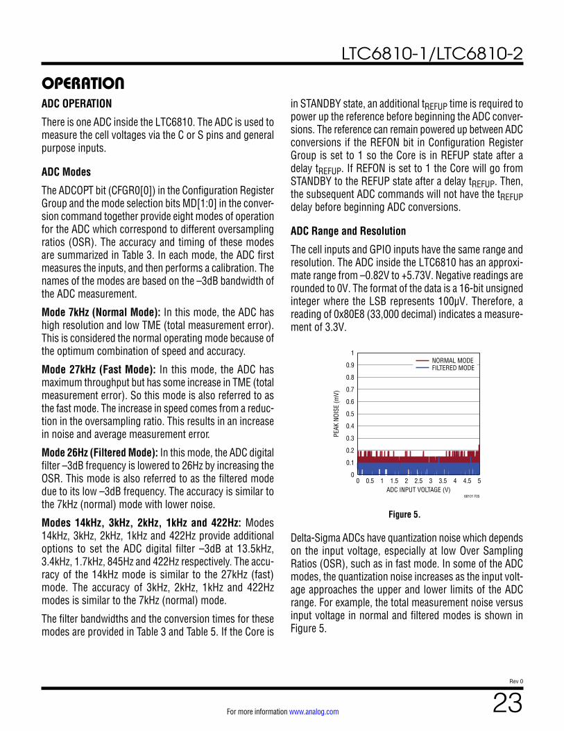
Figure 5.
ADC INPUT VOLTAGE (V)0
PEAK
NOI
SE (m
V)
1
0.1
0.9
0.7
0.5
0.3
0.8
0.6
0.4
0.2
02.5 4.51.5 3.5
68101 F05
52 41 30.5
NORMAL MODEFILTERED MODE
Delta-Sigma ADCs have quantization noise which depends on the input voltage, especially at low Over Sampling Ratios (OSR), such as in fast mode. In some of the ADC modes, the quantization noise increases as the input volt-age approaches the upper and lower limits of the ADC range. For example, the total measurement noise versus input voltage in normal and filtered modes is shown in Figure 5.
LTC6810-1/LTC6810-2
24Rev 0
For more information www.analog.com
OPERATION
The specified range of the ADC is 0V to 5V. In Table 4, the precision range of the ADC is arbitrarily defined as 0.5V to 4.5V. This is the range where the quantization noise is relatively constant even in the lower OSR modes (see Figure 5). Table 4 summarizes the total noise in this range
Table 3. ADC Filter Bandwidth, Accuracy and SpeedMODE –3dB FILTER BW –40dB FILTER BW TME SPEC AT 3.3V, 25°C TME SPEC AT 3.3V, –40°C, 125°C
27kHz (Fast Mode) 27kHz 84kHz ±5.5mV ±5.5mV
14kHz 13.5kHz 42kHz ±5.5mV ±5.5mV
7kHz (Normal Mode) 6.8kHz 21kHz ±1.8mV ±2.4mV
3kHz 3.4kHz 10.5kHz ±1.8mV ±2.4mV
2kHz 1.7kHz 5.3kHz ±1.8mV ±2.4mV
1kHz 845Hz 2.6kHz ±1.8mV ±2.4mV
422Hz 422Hz 1.3kHz ±1.8mV ±2.4mV
26Hz (Filtered Mode) 26Hz 82Hz ±1.8mV ±2.4mV
Note: TME is the total measurement error.
Table 4. ADC Range and Resolution
MODE FULL RANGE1SPECIFIED
RANGEPRECISION
RANGE2 LSB FORMAT MAX NOISENOISE FREE
RESOLUTION3
27kHz (fast)
–0.8192V to 5.7344V 0V to 5V 0.5V to 4.5V 100µV Unsigned 16 Bits
±4mVP-P 10 Bits
14kHz ±1mVP-P 12 Bits
7kHz (normal) ±250µVP-P 14 Bits
3kHz ±150µVP-P 14 Bits
2kHz ±100µVP-P 15 Bits
1kHz ±100µVP-P 15 Bits
422Hz ±100µVP-P 15 Bits
26Hz (filtered) ±50µVP-P 16 Bits
1. Negative readings are rounded to 0V.2. PRECISION RANGE is the range over which the noise is less than MAX NOISE.3. NOISE FREE RESOLUTION is a measure of the noise level within the PRECISION RANGE.
for all eight ADC operating modes. Also shown is the noise free resolution. For example, 14-bit noise free reso-lution in normal mode implies that the top 14 bits will be noise free with a DC input, but that the 15th and 16th least significant bits (LSB) will flicker.
LTC6810-1/LTC6810-2
25Rev 0
For more information www.analog.com
OPERATION
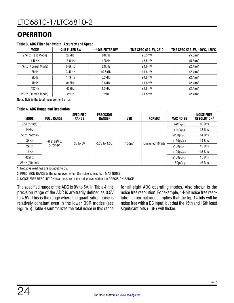
Table 5 shows the conversion times for the ADCV com-mand measuring all six cells. The total conversion time is given by tC which indicates the end of the calibration step.
Figure 7 illustrates the timing of the ADCV command that measures only one cell.
Figure 7.
SERIALINTERFACE
ADCV + PEC
CALIBRATEMEASUREC2 TO C1ADC1
t0 t1M tC68101 F07
tREFUP tCYCLE
Timing for ADCV command measuring 1 cell, SCONV = 0
Figure 6.
SERIALINTERFACE
tCYCLEtSKEW2
ADCV + PEC
MEASUREC5 TO C4
MEASUREC6 TO C5
MEASUREC4 TO C3
MEASUREC3 TO C2
MEASUREC2 TO C1
MEASUREC1 TO C0ADC1
t0 t1M t2M t3M t4M t5M t6M
tREFUP
CALIBRATE
tC68101 F06
Timing for ADCV Command Measuring All 6 Cells, SCONV = 0
Table 5. Conversion and Synchronization Times for ADCV Command Measuring All Six Cells, SCONV = 0CONVERSION TIMES (in µs) SYNCHRONIZATION TIME
(IN µs)
MODE t0 t1M t2M t5M t6M tC,MCAL = 0 tC,MCAL = 1 tSKEW2
27kHz 0 57 104 244 291 524 1,106 233
14kHz 0 87 162 390 465 699 1,281 379
7kHz 0 145 279 681 815 1,165 2,328 670
3kHz 0 261 511 1,262 1,513 1,863 3,026 1,252
2kHz 0 494 977 2,426 2,909 3,259 4,423 2,415
1kHz 0 959 1,908 4,753 5,702 6,052 7,215 4,742
422Hz 0 1,890 3,770 9,408 11,287 11,637 12,801 9,397
26Hz 0 29,818 59,624 149,044 178,851 182,692 201,310 149,033
Table 6 shows the conversion time for ADCV command measuring only 1 cell. tC indicates the total conversion time for this command.Table 6. Conversion Times for ADCV Command Measuring Only One Cell, SCONV = 0
CONVERSION TIMES (in μs)
MODE t0 t1M tC27kHz 0 57 200
14kHz 0 87 229
7kHz 0 145 404
3kHz 0 261 520
2kHz 0 494 753
1kHz 0 959 1,218
422Hz 0 1,890 2,149
26Hz 0 29,817 33,567

LTC6810-1/LTC6810-2
26Rev 0
For more information www.analog.com
OPERATIONUnder/Over Voltage Monitoring
Whenever the C inputs are measured, the results are compared to under voltage and over voltage thresholds stored in memory. If the reading of a cell is above the over voltage limit, a bit in memory is set as a flag. Similarly, measurement results below the under voltage limit cause a flag to be set. The over voltage and under voltage thresh-olds are stored in the Configuration Register Group. The flags are stored in Status Register Group B.
Auxiliary (GPIO) Measurements (ADAX Command)
The ADAX command initiates the measurement of the GPIO inputs. This command has options to select which GPIO input to measure (GPIO1–4) and which ADC mode to use. The ADAX command also measures the S0 pin and the 2nd reference relative to the V– pin voltage. There are options in the ADAX command to measure subsets of S0,
the GPIOs and the 2nd reference separately or to mea-sure S0, all four GPIOs and the 2nd reference in a single command. See the section on Commands for the ADAX command format. All auxiliary measurements are relative to the V– pin voltage. This command can be used to read external temperature by connecting the temperature sen-sors to the GPIOs. These sensors can be powered from the 2nd reference which is also measured by the ADAX command, resulting in precise ratiometric measurements.
Figure 8 illustrates the timing of the ADAX command mea-suring S0, all GPIOs and the 2nd reference. The 2nd refer-ence is measured after GPIO4.
Table 7 shows the conversion time for the ADAX com-mand measuring S0, all the GPIOs and the 2nd reference. tC indicates the total conversion time.
The timing for ADAX measuring a single auxiliary is the same as ADCV measuring a single cell.
Figure 8.
SERIALINTERFACE
tCYCLEtSKEW
ADCV + PEC
MEASUREGPIO4
MEASURE2ND REF
MEASUREGPIO3
MEASUREGPIO2
MEASUREGPIO1
MEASURES0ADC1
t0 t1M t2M t3M t4M t5M t6M
tREFUP
CALIBRATE
tC68101 F08
Timing for ADAX Command Measuring All GPIOs and 2nd Reference
Table 7. Conversion and Synchronization Times for ADAX Command Measuring S0, All GPIOs and 2nd ReferenceCONVERSION TIMES (in µs)
MODE t0 t1M t2M t3M t4M t5M t6M tC,MCAL = 0 tC,MCAL = 1
27kHz 0 57 104 151 197 244 291 521 1,103
14kHz 0 87 162 238 314 390 465 695 1,277
7kHz 0 145 279 413 547 681 815 1,161 2,324
3kHz 0 261 511 762 1,012 1,262 1,513 1,859 3,023
2kHz 0 494 977 1,460 1,943 2,426 2,909 3,255 4,419
1kHz 0 959 1,908 2,856 3,805 4,753 5,702 6,048 7,212
422Hz 0 1,890 3,770 5,649 7,529 9,408 11,287 11,634 12,797
26Hz 0 29,818 59,624 89,431 119,238 149,044 178,851 182,688 201,306
LTC6810-1/LTC6810-2
27Rev 0
For more information www.analog.com
OPERATIONAuxiliary (GPIO) Measurements with Digital Redundancy (ADAXD Command)
The ADAXD command operates similarly to the ADAX command except that an additional diagnostic is per-formed using digital redundancy. See A/D Conversion with Digital Redundancy.
The execution time of ADAX and ADAXD is the same.
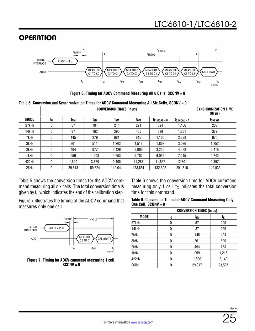
Measuring Cell Voltages and GPIOs (ADCVAX Command)
The ADCVAX command combines six cell measurements with measurements of S0 and GPIO1. This command
simplifies the synchronization of battery cell voltage and current measurements when a current sensor is con-nected to the GPIO1 input. Figure 9 illustrates the timing of ADCVAX command with SCONV set to 0. See the sec-tion on Commands for the ADCVAX command format. The time values in Figure 9 assume the ADC is operating in the 27kHz (fast) mode. The synchronization of the current and voltage measurements, tSKEW1, in fast mode is within 196µs.
Table 8 shows the conversion and synchronization time for the ADCVAX command in different modes with SCONV = 0. The total conversion time for the command is given by tC.
Figure 9.
SERIALINTERFACE
tCYCLEtSKEW1
ADCV + PEC
CALIBRATEMEASUREC6 TO C5
MEASUREC5 TO C4
MEASUREC4 TO C3
MEASUREGPIO1
MEASURES0
MEASUREC3 TO C2
MEASUREC2 TO C1
MEASUREC1 TO C0ADC
t0 t1M t2M t3M t4M t5M t6M t7M t8M tC
tREFUP
68101 F09
Timing of ADCVAX command, SCONV = 0
Table 8. Conversion and Synchronization Times for ADCVAX Command, SCONV = 0
CONVERSION TIMES (in µs)SYNCHRONIZATION
TIME (IN µs)
MODE t0 t1M t2M t3M t4M t5M t6M t7M t8M tC,MCAL = 0 tC,MCAL = 1 tSKEW1
27kHz 0 57 104 151 205 251 305 352 399 682 1,497 194
14kHz 0 87 162 238 321 397 480 556 631 915 1,730 310
7kHz 0 145 279 413 554 688 829 963 1,097 1,497 3,126 543
3kHz 0 261 511 762 1,019 1,270 1,527 1,777 2,028 2,427 4,057 1,008
2kHz 0 494 977 1,460 1,950 2,433 2,923 3,407 3,890 4,289 5,918 1,939
1kHz 0 959 1,908 2,856 3,812 4,760 5,716 6,665 7,613 8,013 9,642 3,801
422Hz 0 1,890 3,770 5,649 7,536 9,415 11,302 13,181 15,060 15,460 17,089 7,525
26Hz 0 29,817 59,624 89,431 119,245 149,051 178,865 208,672 238,479 242,369 268,435 119,234
LTC6810-1/LTC6810-2
28Rev 0
For more information www.analog.com
OPERATIONDATA ACQUISITION SYSTEM DIAGNOSTICS
The battery monitoring data acquisition system is com-prised of a multiplexer, an ADC, 1st reference, digital filters, and memory. To ensure long term reliable perfor-mance there are several diagnostic commands which can be used to verify the proper operation of these circuits.
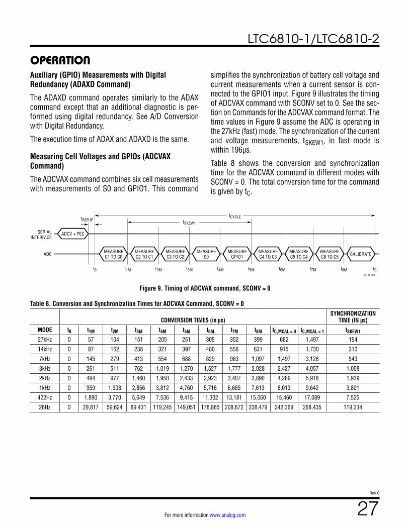
Measuring Internal Device Parameters (ADSTAT Command)
The ADSTAT command is a diagnostic command that measures the following internal device parameters: Sum of All Cells (SC), Internal Die Temperature (ITMP), Analog Power Supply (VA) and Digital Power Supply (VD). These parameters are described in the section below. All the 8 ADC modes described earlier are available for these con-versions. See the section on Commands for the ADSTAT command format.
Figure 10 illustrates the timing of the ADSTAT command measuring all the 4 internal device parameters.
Table 9 shows the conversion time of the ADSTAT com-mand measuring all the 4 internal parameters. tC indicates
Figure 10.
SERIALINTERFACE
tCYCLEtSKEW
ADCV + PEC
MEASUREVD CALIBRATEMEASURE
VAMEASURE
ITMPMEASURE
SCADC
t0 t1M t2M t4Mt3M tC 68101 F10
tREFUP
Timing for ADSTAT command measuring SC, ITMP, VA, VD
Table 9. Conversion and Synchronization Times for ADSTAT Command Measuring SC, ITMP, VA, VD
CONVERSION TIMES (in µs)SYNCHRONIZATION TIME
(in µs)
MODE t0 t1M t2M t3M t4M tC,MCAL = 1 OR 0 tSKEW
27kHz 0 57 104 151 197 741 0 140
14kHz 0 87 162 238 314 858 0 227
7kHz 0 145 279 413 547 1,556 0 402
3kHz 0 261 511 762 1,012 2,021 0 751
2kHz 0 494 977 1,460 1,943 2,952 0 1,449
1kHz 0 959 1,908 2,856 3,805 4,814 0 2,845
422Hz 0 1,890 3,770 5,649 7,528 8,538 0 5,638
26Hz 0 29,817 59,624 89,431 119,237 134,210 0 89,420
the total conversion time for the ADSTAT command. When ADSTAT is performed measuring all 4 internal parameters, the LTC6810 will always perform four calibration cycles, regardless of MCAL.
The timing for ADSTAT measuring a single status param-eter is the same as ADCV measuring a single cell.
Sum of All Cells Measurement: The Sum of All Cells mea-surement is the voltage between V+ and V– with a 10:1 attenuation. The V+ to V– voltage is the same as the total battery voltage when the IC is powered by the battery cells. The 16-bit ADC value of Sum of All Cells measurement (SC) is stored in Status Register Group A. From the SC value, the sum of all cell voltage measurements is given by,
Sum of All Cells = SC • 10 • 100µV
Internal Die Temperature: The ADSTAT command can measure the internal die temperature. The 16 bit ADC value of the die temperature measurement (ITMP) is stored in Status Register Group A. From ITMP, the actual die temperature is calculated using the expression,
Internal Die Temperature (°C) = ITMP •
100µV7.5mV
C – 273 C

LTC6810-1/LTC6810-2
29Rev 0
For more information www.analog.com
OPERATIONPower Supply Measurements: The ADSTAT command is also used to measure the Analog Power Supply (VREG) and Digital Power Supply (VREGD).
The 16 bit ADC value of the analog power supply measure-ment (VA) is stored in Status Register Group A. The 16 bit ADC value of the digital power supply measurement (VD) is stored in Status Register Group B. From VA and VD, the power supply measurements are given by:
Analog Power Supply Measurement (VREG) = VA • 100µV
Digital Power Supply Measurement (VREGD) = VD • 100µV
The value of VREG is determined by external components. VREG should be between 4.5V and 5.5V to maintain accu-racy. The value of VREGD is determined by internal compo-nents. The normal range of VREGD is 2.7V to 3.6V.
Measuring Internal Device Parameters with Digital Redundancy (ADSTATD Command)
The ADSTATD command operates similarly to the ADSTAT command except that an additional diagnostic is performed
using digital redundancy. See the A/D Conversion with Digital Redundancy section.
The execution time of ADSTAT and ADSTATD is the same.
Measuring Cell Voltages and V+ to V– (ADCVSC Command)
The ADCVSC command combines six cell measurements and the measurement of Sum of All Cells. This command simplifies the synchronization of the individual battery cell voltage and the total Sum of All Cells measurement. Figure 11 illustrates the timing of ADCVSC command. See the section on Commands for the ADCVSC com-mand format. The synchronization of the cell voltage and Sum of All Cells measurements, tSKEW, in fast mode is within 147µs.
Table 10 shows the conversion and synchronization time for the ADCVSC command in different modes (with SCONV = 0). The total conversion time for the command is given by tC. When ADCVSC is performed, the LTC6810 will always perform seven calibration cycles, regardless of MCAL.
Figure 11.
SERIALINTERFACE
tCYCLE
tSKEW
ADCV + PEC
CALIBRATEMEASUREC6 TO C5
MEASUREC5 TO C4
MEASUREC4 TO C3
MEASURESC
MEASUREC3 TO C2
MEASUREC2 TO C1
MEASUREC1 TO C0ADC
t0 t1M t2M t3M t4M t5M t6M t7M tC
tREFUP
68101 F11
Timing for ADCVSC Command, SCONV = 0
Table 10. Conversion and Synchronization Times for ADCVSC Command, SCONV = 0
CONVERSION TIMES (in µs)SYNCHRONIZATION TIME
(in µs)
MODE t0 t1M t2M t3M t4M t5M t6M t7M tC,MCAL = 1 OR 0 tSKEW
27kHz 0 57 104 151 205 259 305 352 1,316 147
14kHz 0 87 162 238 321 404 480 556 1,520 235
7kHz 0 145 279 413 554 695 829 963 2,742 409
3kHz 0 261 511 762 1,019 1,277 1,527 1,777 3,556 758
2kHz 0 494 977 1,460 1,950 2,440 2,923 3,407 5,185 1,456
1kHz 0 959 1,908 2,856 3,812 4,768 5,716 6,665 8,443 2,853
422Hz 0 1,890 3,770 5,649 7,536 9,422 11,302 13,181 14,960 5,645
26Hz 0 29,817 59,624 89,431 119,245 149,059 178,865 208,672 234,887 89,427
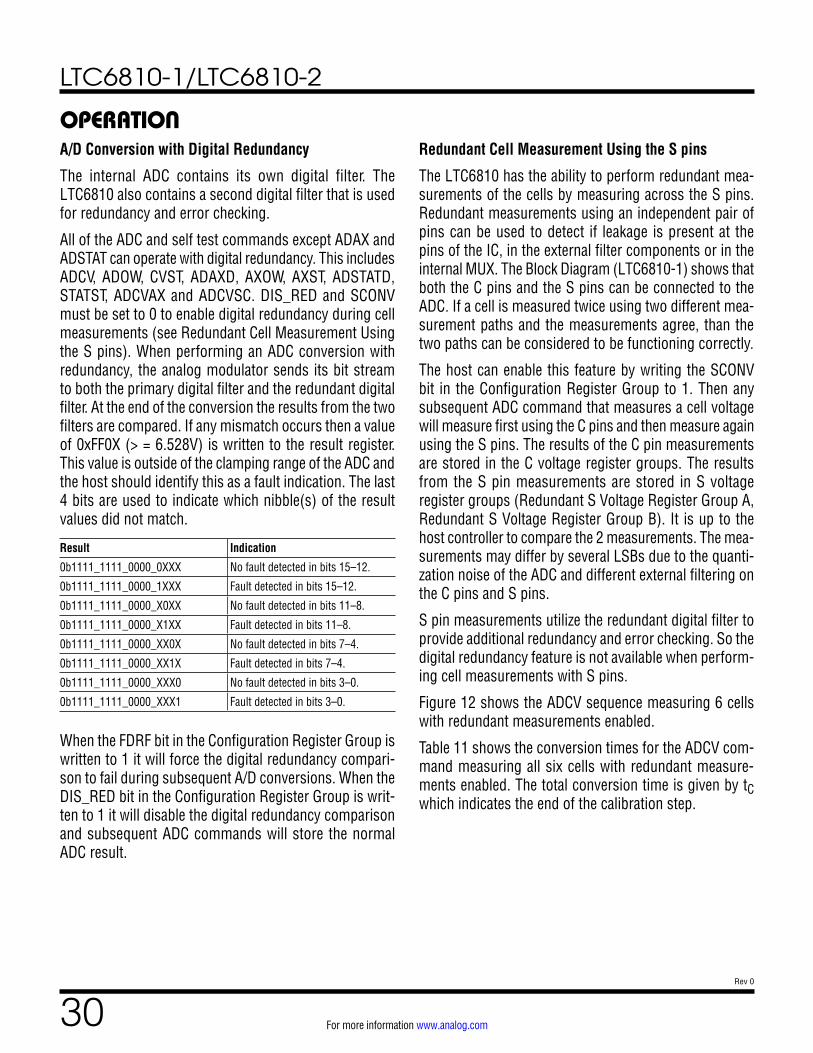
LTC6810-1/LTC6810-2
30Rev 0
For more information www.analog.com
OPERATIONA/D Conversion with Digital Redundancy
The internal ADC contains its own digital filter. The LTC6810 also contains a second digital filter that is used for redundancy and error checking.
All of the ADC and self test commands except ADAX and ADSTAT can operate with digital redundancy. This includes ADCV, ADOW, CVST, ADAXD, AXOW, AXST, ADSTATD, STATST, ADCVAX and ADCVSC. DIS_RED and SCONV must be set to 0 to enable digital redundancy during cell measurements (see Redundant Cell Measurement Using the S pins). When performing an ADC conversion with redundancy, the analog modulator sends its bit stream to both the primary digital filter and the redundant digital filter. At the end of the conversion the results from the two filters are compared. If any mismatch occurs then a value of 0xFF0X (> = 6.528V) is written to the result register. This value is outside of the clamping range of the ADC and the host should identify this as a fault indication. The last 4 bits are used to indicate which nibble(s) of the result values did not match.
Result Indication
0b1111_1111_0000_0XXX No fault detected in bits 15–12.
0b1111_1111_0000_1XXX Fault detected in bits 15–12.
0b1111_1111_0000_X0XX No fault detected in bits 11–8.
0b1111_1111_0000_X1XX Fault detected in bits 11–8.
0b1111_1111_0000_XX0X No fault detected in bits 7–4.
0b1111_1111_0000_XX1X Fault detected in bits 7–4.
0b1111_1111_0000_XXX0 No fault detected in bits 3–0.
0b1111_1111_0000_XXX1 Fault detected in bits 3–0.
When the FDRF bit in the Configuration Register Group is written to 1 it will force the digital redundancy compari-son to fail during subsequent A/D conversions. When the DIS_RED bit in the Configuration Register Group is writ-ten to 1 it will disable the digital redundancy comparison and subsequent ADC commands will store the normal ADC result.
Redundant Cell Measurement Using the S pins
The LTC6810 has the ability to perform redundant mea-surements of the cells by measuring across the S pins. Redundant measurements using an independent pair of pins can be used to detect if leakage is present at the pins of the IC, in the external filter components or in the internal MUX. The Block Diagram (LTC6810-1) shows that both the C pins and the S pins can be connected to the ADC. If a cell is measured twice using two different mea-surement paths and the measurements agree, than the two paths can be considered to be functioning correctly.
The host can enable this feature by writing the SCONV bit in the Configuration Register Group to 1. Then any subsequent ADC command that measures a cell voltage will measure first using the C pins and then measure again using the S pins. The results of the C pin measurements are stored in the C voltage register groups. The results from the S pin measurements are stored in S voltage register groups (Redundant S Voltage Register Group A, Redundant S Voltage Register Group B). It is up to the host controller to compare the 2 measurements. The mea-surements may differ by several LSBs due to the quanti-zation noise of the ADC and different external filtering on the C pins and S pins.
S pin measurements utilize the redundant digital filter to provide additional redundancy and error checking. So the digital redundancy feature is not available when perform-ing cell measurements with S pins.
Figure 12 shows the ADCV sequence measuring 6 cells with redundant measurements enabled.
Table 11 shows the conversion times for the ADCV com-mand measuring all six cells with redundant measure-ments enabled. The total conversion time is given by tCwhich indicates the end of the calibration step.

LTC6810-1/LTC6810-2
31Rev 0
For more information www.analog.com
OPERATION
Figure 13 illustrates the timing of the ADCV command that measures one cell with redundant measurement.
Table 12 shows the conversion time for ADCV command measuring only 1 cell. tC indicates the total conversion time for this command.
Figure 14 illustrates the timing of the ADCVAX command with SCONV set to 1.
Table 13 shows the conversion and synchronization time for the ADCVAX command in different modes with SCONV set to 1. The total conversion time for the command is given by tC.
Figure 15 illustrates the timing of the ADCVSC command with SCONV set to 1.
Table 14 shows the conversion and synchronization time for the ADCVSC command in different modes with SCONV set to 1. The total conversion time for the command is given by tC.
Figure 12.
SERIALINTERFACE
tCYCLE
MEASURES2 TO S1 CALIBRATEMEASURE
S1 TO S0MEASUREC1 TO C0ADC
t0 t1M t2M t4M t10M tC68101 F12
tREFUP
MEASUREC2 TO C21
t3M
MEASUREC6 TO C5
t11M t12M
MEASURES6 TO S5
ADCV + PEC
Timing for ADCV Command Measuring All 6 Cells, SCONV = 1
Table 11. Conversion Times for ADCV Command Measuring All Six Cells, SCONV = 1CONVERSION TIMES (in µs)
MODE t0 t1M t2M t3M t4M t5M t6M t7M t8M t9M t10M t11M t12M tC,MCAL = 0 tC,MCAL = 1
27kHz 0 57 104 151 197 244 291 337 384 431 477 524 571 913 2,194
14kHz 0 87 163 238 314 390 466 541 617 693 769 844 920 1,263 2,543
7kHz 0 145 279 413 547 680 814 948 1,082 1,216 1,350 1,484 1,618 2,077 4,637
3kHz 0 261 511 762 1,012 1,262 1,513 1,763 2,013 2,263 2,514 2,764 3,014 3,473 6,033
2kHz 0 494 977 1,460 1,943 2,426 2,909 3,392 3,875 4,358 4,841 5,324 5,807 6,266 8,827
1kHz 0 959 1,908 2,856 3,805 4,753 5,702 6,650 7,599 8,547 9,496 10,444 11,393 11,852 14,412
422Hz 0 1,890 3,770 5,649 7,528 9,408 11,287 13,167 15,046 16,925 18,805 20,684 22,563 23,023 25,583
26Hz 0 29,818 59,624 89,431 119,238 149,044 178,851 208,658 238,464 268,271 298,078 327,884 357,691 361,641 402,601
Figure 13.
MEASURES2 TO S1
MEASUREC2 TO C1ADC2
SERIALINTERFACE
CALIBRATE
ADCV + PEC
t0 t1M t2M tC68101 F13
tREFUP tCYCLE
Timing for ADCV Command Measuring One Cell, SCONV = 1
Table 12. Conversion Times for ADCV Command Measuring Only One Cell, SCONV = 1
CONVERSION TIMES (in µs)
MODE t0 t1M t2M tC,MCAL = 0 tC,MCAL = 1
27kHz 0 57 104 265 381
14kHz 0 87 162 323 440
7kHz 0 145 279 556 789
3kHz 0 261 512 789 1,021
2kHz 0 494 977 1,254 1,487
1kHz 0 959 1,908 2,185 2,418
422Hz 0 1,890 3,770 4,047 4,280
26Hz 0 29,817 59,624 63,392 67,116
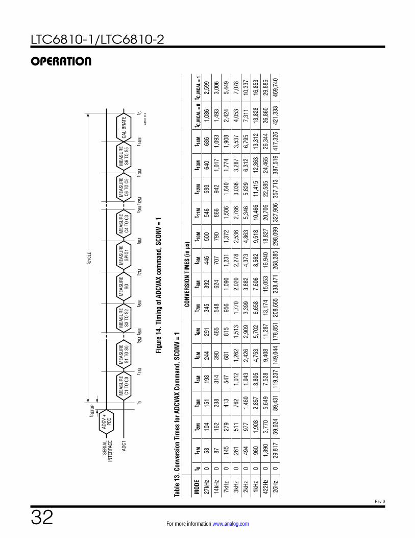
LTC6810-1/LTC6810-2
32Rev 0
For more information www.analog.com
OPERATION
Figu
re 1
4.
SERI
ALIN
TERF
ACE
t CYC
LE
MEA
SURE
C4 T
O C3
CALI
BRAT
EM
EASU
RESO
MEA
SURE
S3 T
O S2
MEA
SURE
S1 T
O S0
MEA
SURE
C1 T
O C0
ADCV
+PE
C
ADC1
t 0t 1
Mt 2
Mt 6
Mt 5
Mt 7
Mt 9
Mt 12
Mt C
6810
1 F1
4
t REF
UP
MEA
SURE
GPIO
1
t 8M
MEA
SURE
C6 T
O C5
t 13M
t 14M
MEA
SURE
S6 T
O S5
Tim
ing
of A
DCVA
X co
mm
and,
SCO
NV =
1
Tabl
e 13
. Con
vers
ion
Tim
es fo
r ADC
VAX
Com
man
d, S
CONV
= 1
CONV
ERSI
ON T
IMES
(in
µs)
MOD
Et 0
t 1M
t 2M
t 3M
t 4M
t 5M
t 6M
t 7M
t 8M
t 9M
t 10M
t 11M
t 12M
t 13M
t 14M
t C,M
CAL
= 0
t C,M
CAL
= 1
27kH
z0
5810
415
119
824
429
134
539
244
650
054
659
364
068
61,
086
2,59
9
14kH
z0
8716
223
831
439
046
554
862
470
779
086
694
21,
017
1,09
31,
493
3,00
6
7kHz
014
527
941
354
768
181
595
61,
090
1,23
11,
372
1,50
61,
640
1,77
41,
908
2,42
45,
449
3kHz
026
151
176
21,
012
1,26
21,
513
1,77
02,
020
2,27
82,
536
2,78
63,
036
3,28
73,
537
4,05
37,
078
2kHz
049
497
71,
460
1,94
32,
426
2,90
93,
399
3,88
24,
373
4,86
35,
346
5,82
96,
312
6,79
57,
311
10,3
37
1kHz
096
01,
908
2,85
73,
805
4,75
35,
702
6,65
87,
606
8,56
29,
518
10,4
6611
,415
12,3
6313
,312
13,8
2816
,853
422H
z0
1,89
03,
770
5,64
97,
528
9,40
811
,287
13,1
7415
,053
16,9
4018
,827
20,7
0622
,585
24,4
6526
,344
26,8
6029
,886
26Hz
029
,817
59,6
2489
,431
119,
237
149,
044
178,
851
208,
665
238,
471
268,
285
298,
099
327,
906
357,
713
387,
519
417,
326
421,
333
469,
740
LTC6810-1/LTC6810-2
33Rev 0
For more information www.analog.com
OPERATION
Figu
re 1
5.
SERI
ALIN
TERF
ACE
t CYC
LE
MEA
SURE
S4 T
O S3
CALI
BRAT
EM
EASU
RESC
MEA
SURE
S3 T
O S2
MEA
SURE
S1 T
O S0
MEA
SURE
C1 T
O C0
ADCV
+PE
C
ADC1
t 0t 1
Mt 2
Mt 6
Mt 5
Mt 7
Mt 9
Mt 11
Mt C
6810
1 F1
5
t REF
UP
MEA
SURE
C4 T
O C3
t 8M
MEA
SURE
C6 T
O C5
t 12M
t 13M
MEA
SURE
S6 T
O S5
Tim
ing
of A
DCVA
X co
mm
and,
SCO
NV =
1
Tabl
e 14
. Con
vers
ion
Tim
es fo
r ADC
VSC
Com
man
d, S
CONV
= 1
CONV
ERSI
ON T
IMES
(in
µs)
MOD
Et 0
t 1M
t 2M
t 3M
t 4M
t 5M
t 6M
t 7M
t 8M
t 9M
t 10M
t 11M
t 12M
t 13M
t C,M
CAL
= 0
t C,M
CAL
= 1
27kH
z0
5810
415
119
824
429
134
539
945
350
054
659
364
02,
418
2,41
8
14kH
z0
8716
223
831
439
046
554
863
171
479
086
694
21,
017
2,79
62,
796
7kHz
014
527
941
354
768
181
595
61,
097
1,23
81,
372
1,50
61,
640
1,77
45,
065
5,06
5
3kHz
026
151
176
21,
012
1,26
21,
513
1,77
02,
028
2,28
52,
536
2,78
63,
036
3,28
76,
578
6,57
8
2kHz
049
497
71,
460
1,94
32,
426
2,90
93,
399
3,89
04,
380
4,86
35,
346
5,82
96,
312
9,60
39,
603
1kHz
096
01,
908
2,85
73,
805
4,75
35,
702
6,65
87,
613
8,56
99,
518
10,4
6611
,415
12,3
6315
,654
15,6
54
422H
z0
1,89
03,
770
5,64
97,
528
9,40
811
,287
13,1
7415
,060
16,9
4718
,827
20,7
0622
,585
24,4
6527
,756
27,7
56
26Hz
029
,817
59,6
2489
,431
119,
237
149,
044
178,
851
208,
665
238,
479
268,
293
298,
099
327,
906
357,
713
387,
519
436,
192
436,
192
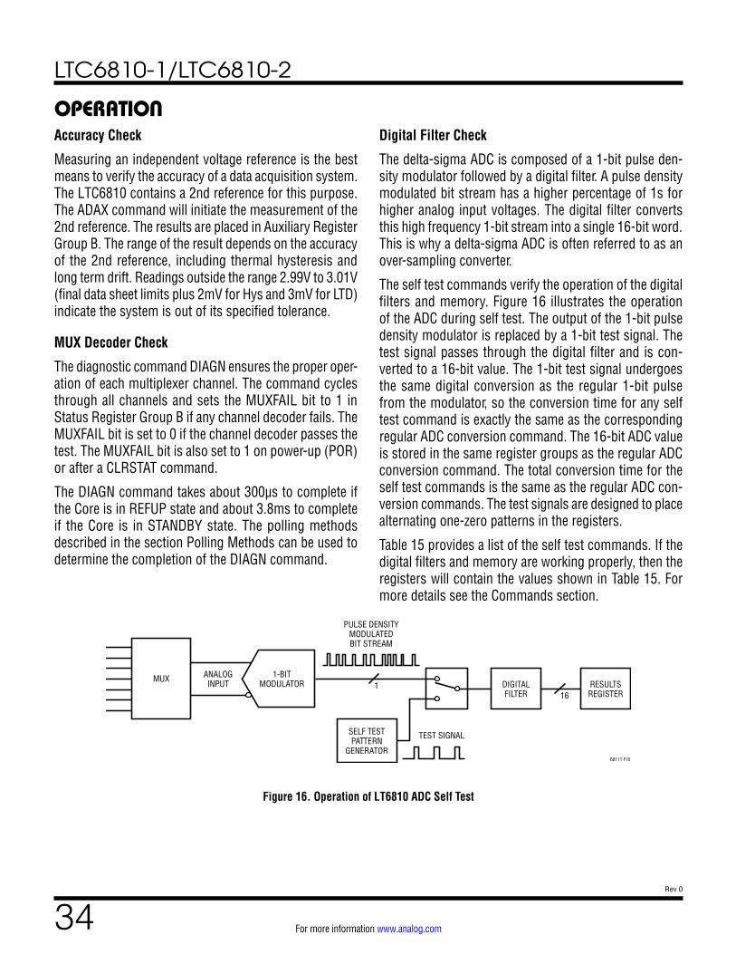
LTC6810-1/LTC6810-2
34Rev 0
For more information www.analog.com
OPERATION
68111 F10
RESULTSREGISTER
DIGITALFILTER
ANALOGINPUTMUX
TEST SIGNAL
PULSE DENSITYMODULATEDBIT STREAM
1
SELF TESTPATTERN
GENERATOR
16
1-BITMODULATOR
Figure 16. Operation of LT6810 ADC Self Test
Accuracy Check
Measuring an independent voltage reference is the best means to verify the accuracy of a data acquisition system. The LTC6810 contains a 2nd reference for this purpose. The ADAX command will initiate the measurement of the 2nd reference. The results are placed in Auxiliary Register Group B. The range of the result depends on the accuracy of the 2nd reference, including thermal hysteresis and long term drift. Readings outside the range 2.99V to 3.01V (final data sheet limits plus 2mV for Hys and 3mV for LTD) indicate the system is out of its specified tolerance.
MUX Decoder Check
The diagnostic command DIAGN ensures the proper oper-ation of each multiplexer channel. The command cycles through all channels and sets the MUXFAIL bit to 1 in Status Register Group B if any channel decoder fails. The MUXFAIL bit is set to 0 if the channel decoder passes the test. The MUXFAIL bit is also set to 1 on power-up (POR) or after a CLRSTAT command.
The DIAGN command takes about 300µs to complete if the Core is in REFUP state and about 3.8ms to complete if the Core is in STANDBY state. The polling methods described in the section Polling Methods can be used to determine the completion of the DIAGN command.
Digital Filter Check
The delta-sigma ADC is composed of a 1-bit pulse den-sity modulator followed by a digital filter. A pulse density modulated bit stream has a higher percentage of 1s for higher analog input voltages. The digital filter converts this high frequency 1-bit stream into a single 16-bit word. This is why a delta-sigma ADC is often referred to as an over-sampling converter.
The self test commands verify the operation of the digital filters and memory. Figure 16 illustrates the operation of the ADC during self test. The output of the 1-bit pulse density modulator is replaced by a 1-bit test signal. The test signal passes through the digital filter and is con-verted to a 16-bit value. The 1-bit test signal undergoes the same digital conversion as the regular 1-bit pulse from the modulator, so the conversion time for any self test command is exactly the same as the corresponding regular ADC conversion command. The 16-bit ADC value is stored in the same register groups as the regular ADC conversion command. The total conversion time for the self test commands is the same as the regular ADC con-version commands. The test signals are designed to place alternating one-zero patterns in the registers.
Table 15 provides a list of the self test commands. If the digital filters and memory are working properly, then the registers will contain the values shown in Table 15. For more details see the Commands section.
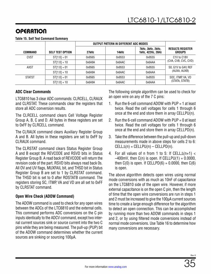
LTC6810-1/LTC6810-2
35Rev 0
For more information www.analog.com
OPERATION
ADC Clear Commands
LTC6810 has 3 clear ADC commands: CLRCELL, CLRAUX and CLRSTAT. These commands clear the registers that store all ADC conversion results.
The CLRCELL command clears Cell Voltage Register Group A, B, C and D. All bytes in these registers are set to 0xFF by CLRCELL command.
The CLRAUX command clears Auxiliary Register Group A and B. All bytes in these registers are set to 0xFF by CLRAUX command.
The CLRSTAT command clears Status Register Group A and B except the REVCODE and RSVD bits in Status Register Group B. A read back of REVCODE will return the revision code of the part. RSVD bits always read back 0s. All OV and UV flags, MUXFAIL bit, and THSD bit in Status Register Group B are set to 1 by CLRSTAT command. The THSD bit is set to 0 after RDSTATB command. The registers storing SC, ITMP, VA and VD are all set to 0xFF by CLRSTAT command.
Open Wire Check (ADOW Command)
The ADOW command is used to check for any open wires between the ADCs of the LTC6810 and the external cells. This command performs ADC conversions on the C pin inputs identically to the ADCV command, except two inter-nal current sources sink or source current into the two C pins while they are being measured. The pull-up (PUP) bit of the ADOW command determines whether the current sources are sinking or sourcing 100µA.
The following simple algorithm can be used to check for an open wire on any of the 7 C pins:
1. Run the 6-cell command ADOW with PUP = 1 at least twice. Read the cell voltages for cells 1 through 6 once at the end and store them in array CELLPU(n).
2. Run the 6-cell command ADOW with PUP = 0 at least twice. Read the cell voltages for cells 1 through 6 once at the end and store them in array CELLPD(n).
3. Take the difference between the pull-up and pull-down measurements made in above steps for cells 2 to 6: CELL∆(n) = CELLPU(n) – CELLPD(n).
4. For all values of n from 1 to 5: If CELL∆(n+1) < –400mV, then C(n) is open. If CELLPU(1) = 0.0000, then C(0) is open. If CELLPD(6) = 0.0000, then C(6) is open.
The above algorithm detects open wires using normal mode conversions with as much as 10nF of capacitance on the LTC6810 side of the open wire. However, if more external capacitance is on the open C pin, then the length of time that the open wire conversions are run in steps 1 and 2 must be increased to give the 100µA current sources time to create a large enough difference for the algorithm to detect an open connection. This can be accomplished by running more than two ADOW commands in steps 1 and 2, or by using filtered mode conversions instead of normal mode conversions. Use Table 16 to determine how many conversions are necessary.
Table 15. Self Test Command Summary
COMMAND SELF TEST OPTION
OUTPUT PATTERN IN DIFFERENT ADC MODES
RESULTS REGISTER GROUPS27kHz 14kHz
7kHz, 3kHz, 2kHz, 1kHz, 422Hz, 26Hz
CVST ST[1:0] = 01 0x9565 0x9553 0x9555 C1V to C18V (CVA, CVB, CVC, CVD)ST[1:0] = 10 0x6A9A 0x6AAC 0x6AAA
AXST ST[1:0] = 01 0x9565 0x9553 0x9555 S0, G1V to G4V, REF (AUXA, AUXB)ST[1:0] = 10 0x6A9A 0x6AAC 0x6AAA
STATST ST[1:0] = 01 0x9565 0x9553 0x9555 SOC, ITMP, VA, VD (STATA, STATB)ST[1:0] = 10 0x6A9A 0x6AAC 0x6AAA
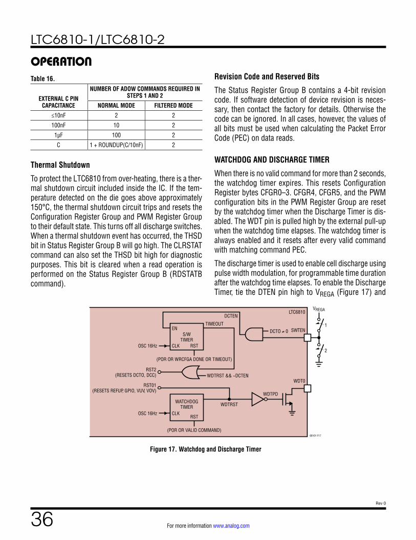
LTC6810-1/LTC6810-2
36Rev 0
For more information www.analog.com
OPERATIONTable 16.
EXTERNAL C PIN CAPACITANCE
NUMBER OF ADOW COMMANDS REQUIRED IN STEPS 1 AND 2
NORMAL MODE FILTERED MODE
≤10nF 2 2
100nF 10 2
1µF 100 2
C 1 + ROUNDUP(C/10nF) 2
Thermal Shutdown
To protect the LTC6810 from over-heating, there is a ther-mal shutdown circuit included inside the IC. If the tem-perature detected on the die goes above approximately 150°C, the thermal shutdown circuit trips and resets the Configuration Register Group and PWM Register Group to their default state. This turns off all discharge switches. When a thermal shutdown event has occurred, the THSD bit in Status Register Group B will go high. The CLRSTAT command can also set the THSD bit high for diagnostic purposes. This bit is cleared when a read operation is performed on the Status Register Group B (RDSTATB command).
Revision Code and Reserved Bits
The Status Register Group B contains a 4-bit revision code. If software detection of device revision is neces-sary, then contact the factory for details. Otherwise the code can be ignored. In all cases, however, the values of all bits must be used when calculating the Packet Error Code (PEC) on data reads.
WATCHDOG AND DISCHARGE TIMER
When there is no valid command for more than 2 seconds, the watchdog timer expires. This resets Configuration Register bytes CFGR0–3. CFGR4, CFGR5, and the PWM configuration bits in the PWM Register Group are reset by the watchdog timer when the Discharge Timer is dis-abled. The WDT pin is pulled high by the external pull-up when the watchdog time elapses. The watchdog timer is always enabled and it resets after every valid command with matching command PEC.
The discharge timer is used to enable cell discharge using pulse width modulation, for programmable time duration after the watchdog time elapses. To enable the Discharge Timer, tie the DTEN pin high to VREGA (Figure 17) and
68101 F17
VREGA
SWTEN
LTC6810
DCTO ≠ 0
2
S/WTIMER
TIMEOUT
DCTEN
EN
RSTCLK
1
RST
(POR OR WRCFGA DONE OR TIMEOUT)
(POR OR VALID COMMAND)
CLK
OSC 16Hz
OSC 16Hz
WDT0
WDTPD
WDTRST && ~DCTENRST2
(RESETS DCTO, DCC)
RST01(RESETS REFUP, GPIO, VUV, VOV)
WDTRSTWATCHDOGTIMER
Figure 17. Watchdog and Discharge Timer

LTC6810-1/LTC6810-2
37Rev 0
For more information www.analog.com
OPERATION
write the DCTO value in the Configuration Register Group to a non-zero value. Once the watchdog time elapses, the discharge switches are now allowed to discharge at a duty cycle specified by the PWM configuration bits in the PWM Register Group for a time duration that is deter-mined by the DCTO value. Table 17 shows the various time settings and the corresponding DCTO value. Table 18 summarizes the status of the Configuration Register Group after a watchdog timer or discharge timer event.
The status of the discharge timer can be determined by reading the configuration register using the RDCFG com-mand. The DCTO value indicates the time left before the Discharge Timer expires as shown in Table 19.
Unlike the watchdog timer, the discharge timer does not reset when there is a valid command. The discharge timer is only reset after a valid WRCFG (Write Configuration Register Group) command. There is a possibility that the Discharge Timer will expire in the middle of some commands.
If Discharge Timer expires in the middle of WRCFG command, the Configuration Register Group and PWM Register Group reset as per Table 18. However, at the end of the valid WRCFG command, the new data is copied to the configuration register. The new data is not lost when the Discharge Timer fired.
If Discharge Timer fires in the middle of RDCFG com-mand, the Configuration Register Group resets as per Table 18. As a result, the read back data from bytes CRFG4 and CRFG5 could be corrupted. If Discharge Timer fires in the middle of WRPWM or RDPWM command, the PWM Register Group resets as per Table 18. As a result, the data could be corrupted.
Table 17. DCTO SettingsDCTO 0 1 2 3 4 5 6 7 8 9 A B C D E FTime (min) Disabled 0.5 1 2 3 4 5 10 15 20 30 40 60 75 90 120
Table 18
WATCHDOG TIMER DISCHARGE TIMER
DTEN = 0, DCTO = XXXX
Resets CFGR0-5 and PWM bits when it fires.
Disabled
DTEN = 1, DCTO = 0000
Resets CFGR0-5 and PWM bits when it fires.
Disabled
DTEN = 1, DCTO != 0000
Resets CFGR0-3 when it fires.
Resets CFGR4-5 and PWM bits when it fires.
Table 19. DCTO (READ VALUE) TIME LEFT (MIN)
0 Disabled (or) Discharge Timer Has Timed Out
1 0 < Timer ≤ 0.5
2 0.5 < Timer ≤ 1
3 1 < Timer ≤ 2
4 2 < Timer ≤ 3
5 3 < Timer ≤ 4
6 4 < Timer ≤ 5
7 5 < Timer ≤ 10
8 10 < Timer ≤ 15
9 15 < Timer ≤ 20
A 20 < Timer ≤ 30
B 30 < Timer ≤ 40
C 40 < Timer ≤ 60
D 60 < Timer ≤ 75
E 75 < Timer ≤ 90
F 90 < Timer ≤ 120

LTC6810-1/LTC6810-2
38Rev 0
For more information www.analog.com
OPERATIONS PIN PULSE WIDTH MODULATION FOR CELL BALANCING
While the watchdog timer is not expired, the DCC bits in the Configuration Register Group control the S pins directly. After the watchdog timer expires, PWM operation begins and continues for the remainder of the selected software discharge time or until a wake-up event occurs (and the watchdog timer is reset).
Once PWM operation begins, the configurations in the PWM Register Group control the S pins to achieve the desired duty cycle as shown in Table 20. Each PWM signal operates on a 30 second period. For each cell, the duty-cycle can be programmed from 0% to 50% duty cycle in increments of 1/30 = 3.33% (1 second). S pins for adja-cent cells are never activated at the same time, hence the maximum 50% duty cycle. There is a non-overlap of at least 1ms between activation of any two adjacent S pins.
Table 20. PWM ConfigurationsDTEN
SETTINGPWMC
SETTINGON TIME
[SECONDS]OFF TIME
[SECONDS]DUTY CYCLE
[%]
1’b0 4’bXXXX 0 Continuously Off 0
1’b1 4’b1111 15 15 50
1’b1 4’b1110 14 16 46.7
1’b1 4’b1101 13 17 43.3
1’b1 4’b1100 12 18 40
1’b1 4’b1011 11 19 36.7
1’b1 4’b1010 10 20 33.3
1’b1 4’b1001 9 21 30
1’b1 4’b1000 8 22 26.7
1’b1 4’b0111 7 23 23.3
1’b1 4’b0110 6 24 20
1’b1 4’b0101 5 25 16.7
1’b1 4’b0100 4 26 13.3
1’b1 4’b0011 3 27 10
1’b1 4’b0010 2 28 6.7
1’b1 4’b0001 1 29 3.3
1’b1 4’b0000 0 Continuously Off 0
The PWM turn on/off times for the S pins are sequenced at different intervals so that no two pins switch on or off
at the same time. The switching interval between chan-nels is 62.5ms, and 375ms are required for all 6 pins to switch (6 • 62.5ms).
The default value of the PWMC settings in the PWM Register Group is all 0s. Upon entry to sleep mode, the PWMC settings will be reset to their default value.
DISCHARGE TIMER MONITOR
The LTC6810 has the ability to periodically monitor cell voltages while the discharge timer is active. The host should write the DTEN bit in the Configuration Register Group to 1 to enable this feature.
When the discharge timer monitor is enabled and the watchdog timer has expired, the LTC6810 will perform a conversion of all cell voltages in 7kHz (Normal) Mode every 30 seconds. The overvoltage and undervoltage comparisons will be performed and flags will be set if cells have crossed a threshold. For any undervoltage cells the discharge timer monitor will automatically clear the associated PWMC bits in the PWM Register Group so that the cell will no longer be discharged. Clearing the Discharge Control bit will also disable PWM discharge. With this feature, the host can write the undervoltage threshold to the desired discharge level and use the dis-charge timer monitor to discharge all, or selected, cells down to that level.
During discharge timer monitoring, digital redundancy checking will be performed on the cell voltage measure-ments. If a digital redundancy failure occurs, all PWMC bits will be cleared and discharge will be terminated.
I2C/SPI MASTER ON LTC6810 USING GPIOS
The I/O ports GPIO2, GPIO3 and GPIO4 on LTC6810 can be used as an I2C or SPI master port to communicate to an I2C or SPI slave. In case of I2C master, GPIO3 and GPIO4 form the SDA and SCL ports of the I2C interface respectively. In case of SPI master, GPIO2, GPIO3 and GPIO4 become the CSB, SDIO and SCK ports of the SPI interface respectively. The SPI master on LTC6810 sup-ports SPI mode 3 (CHPA = 1, CPOL = 1).
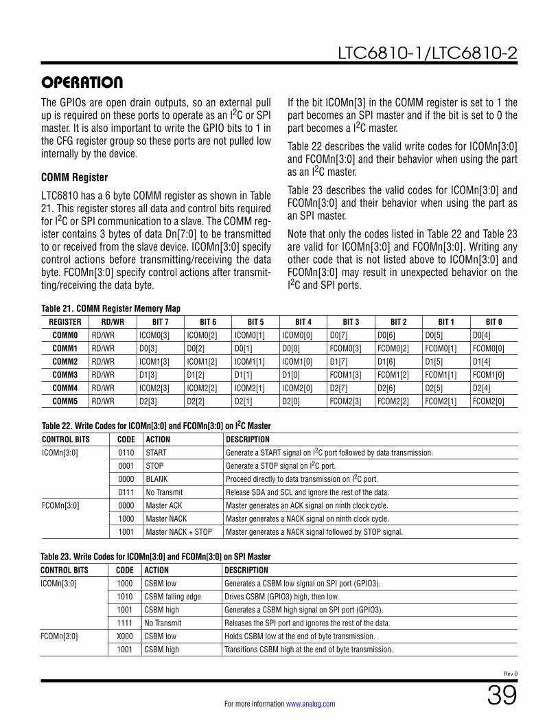
LTC6810-1/LTC6810-2
39Rev 0
For more information www.analog.com
OPERATIONThe GPIOs are open drain outputs, so an external pull up is required on these ports to operate as an I2C or SPI master. It is also important to write the GPIO bits to 1 in the CFG register group so these ports are not pulled low internally by the device.
COMM Register
LTC6810 has a 6 byte COMM register as shown in Table 21. This register stores all data and control bits required for I2C or SPI communication to a slave. The COMM reg-ister contains 3 bytes of data Dn[7:0] to be transmitted to or received from the slave device. ICOMn[3:0] specify control actions before transmitting/receiving the data byte. FCOMn[3:0] specify control actions after transmit-ting/receiving the data byte.
If the bit ICOMn[3] in the COMM register is set to 1 the part becomes an SPI master and if the bit is set to 0 the part becomes a I2C master.
Table 22 describes the valid write codes for ICOMn[3:0] and FCOMn[3:0] and their behavior when using the part as an I2C master.
Table 23 describes the valid codes for ICOMn[3:0] and FCOMn[3:0] and their behavior when using the part as an SPI master.
Note that only the codes listed in Table 22 and Table 23 are valid for ICOMn[3:0] and FCOMn[3:0]. Writing any other code that is not listed above to ICOMn[3:0] and FCOMn[3:0] may result in unexpected behavior on the I2C and SPI ports.
Table 21. COMM Register Memory MapREGISTER RD/WR BIT 7 BIT 6 BIT 5 BIT 4 BIT 3 BIT 2 BIT 1 BIT 0
COMM0 RD/WR ICOM0[3] ICOM0[2] ICOM0[1] ICOM0[0] D0[7] D0[6] D0[5] D0[4]
COMM1 RD/WR D0[3] D0[2] D0[1] D0[0] FCOM0[3] FCOM0[2] FCOM0[1] FCOM0[0]
COMM2 RD/WR ICOM1[3] ICOM1[2] ICOM1[1] ICOM1[0] D1[7] D1[6] D1[5] D1[4]
COMM3 RD/WR D1[3] D1[2] D1[1] D1[0] FCOM1[3] FCOM1[2] FCOM1[1] FCOM1[0]
COMM4 RD/WR ICOM2[3] ICOM2[2] ICOM2[1] ICOM2[0] D2[7] D2[6] D2[5] D2[4]
COMM5 RD/WR D2[3] D2[2] D2[1] D2[0] FCOM2[3] FCOM2[2] FCOM2[1] FCOM2[0]
Table 22. Write Codes for ICOMn[3:0] and FCOMn[3:0] on I2C MasterCONTROL BITS CODE ACTION DESCRIPTION
ICOMn[3:0] 0110 START Generate a START signal on I2C port followed by data transmission.
0001 STOP Generate a STOP signal on I2C port.
0000 BLANK Proceed directly to data transmission on I2C port.
0111 No Transmit Release SDA and SCL and ignore the rest of the data.
FCOMn[3:0] 0000 Master ACK Master generates an ACK signal on ninth clock cycle.
1000 Master NACK Master generates a NACK signal on ninth clock cycle.
1001 Master NACK + STOP Master generates a NACK signal followed by STOP signal.
Table 23. Write Codes for ICOMn[3:0] and FCOMn[3:0] on SPI MasterCONTROL BITS CODE ACTION DESCRIPTION
ICOMn[3:0] 1000 CSBM low Generates a CSBM low signal on SPI port (GPIO3).
1010 CSBM falling edge Drives CSBM (GPIO3) high, then low.
1001 CSBM high Generates a CSBM high signal on SPI port (GPIO3).
1111 No Transmit Releases the SPI port and ignores the rest of the data.
FCOMn[3:0] X000 CSBM low Holds CSBM low at the end of byte transmission.
1001 CSBM high Transitions CSBM high at the end of byte transmission.
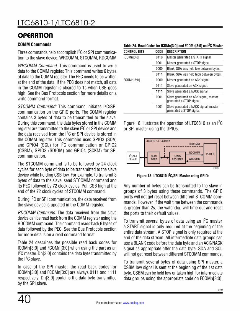
LTC6810-1/LTC6810-2
40Rev 0
For more information www.analog.com
OPERATIONCOMM Commands
Three commands help accomplish I2C or SPI communica-tion to the slave device: WRCOMM, STCOMM, RDCOMM
WRCOMM Command: This command is used to write data to the COMM register. This command writes 6 bytes of data to the COMM register. The PEC needs to be written at the end of the data. If the PEC does not match, all data in the COMM register is cleared to 1s when CSB goes high. See the Bus Protocols section for more details on a write command format.
STCOMM Command: This command initiates I2C/SPI communication on the GPIO ports. The COMM register contains 3 bytes of data to be transmitted to the slave. During this command, the data bytes stored in the COMM register are transmitted to the slave I2C or SPI device and the data received from the I2C or SPI device is stored in the COMM register. This command uses GPIO3 (SDA) and GPIO4 (SCL) for I2C communication or GPIO2 (CSBM), GPIO3 (SDIOM) and GPIO4 (SCKM) for SPI communication.
The STCOMM command is to be followed by 24 clock cycles for each byte of data to be transmitted to the slave device while holding CSB low. For example, to transmit 3 bytes of data to the slave, send STCOMM command and its PEC followed by 72 clock cycles. Pull CSB high at the end of the 72 clock cycles of STCOMM command.
During I2C or SPI communication, the data received from the slave device is updated in the COMM register.
RDCOMM Command: The data received from the slave device can be read back from the COMM register using the RDCOMM command. The command reads back 6 bytes of data followed by the PEC. See the Bus Protocols section for more details on a read command format.
Table 24 describes the possible read back codes for ICOMn[3:0] and FCOMn[3:0] when using the part as an I2C master. Dn[3:0] contains the data byte transmitted by the I2C slave.
In case of the SPI master, the read back codes for ICOMn[3:0] and FCOMn[3:0] are always 0111 and 1111 respectively. Dn[3:0] contains the data byte transmitted by the SPI slave.
Table 24. Read Codes for ICOMn[3:0] and FCOMn[3:0] on I2C MasterCONTROL BITS CODE DESCRIPTION
ICOMn[3:0] 0110 Master generated a START signal.
0001 Master generated a STOP signal.
0000 Blank, SDA was held low between bytes.
0111 Blank, SDA was held high between bytes.
FCOMn[3:0] 0000 Master generated an ACK signal.
0111 Slave generated an ACK signal.
1111 Slave generated a NACK signal.
0001 Slave generated an ACK signal, master generated a STOP signal.
1001 Slave generated a NACK signal, master generated a STOP signal.
Figure 18 illustrates the operation of LTC6810 as an I2C or SPI master using the GPIOs.
Figure 18.
68101 F18
COMMREGISTER
GPIOPORT
I2C/SPISLAVE
PORT ARDCOMM
WRCOMM
STCOMMLTC6810-1/LTC6810-2
LTC6810 I2C/SPI Master using GPIOs
Any number of bytes can be transmitted to the slave in groups of 3 bytes using these commands. The GPIO ports will not get reset between different STCOMM com-mands. However, if the wait time between the commands is greater than 2s, the watchdog will time out and reset the ports to their default values.
To transmit several bytes of data using an I2C master, a START signal is only required at the beginning of the entire data stream. A STOP signal is only required at the end of the data stream. All intermediate data groups can use a BLANK code before the data byte and an ACK/NACK signal as appropriate after the data byte. SDA and SCL will not get reset between different STCOMM commands.
To transmit several bytes of data using SPI master, a CSBM low signal is sent at the beginning of the 1st data byte. CSBM can be held low or taken high for intermediate data groups using the appropriate code on FCOMn[3:0].
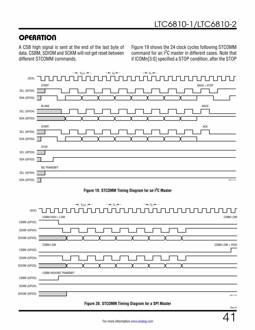
LTC6810-1/LTC6810-2
41Rev 0
For more information www.analog.com
OPERATIONA CSB high signal is sent at the end of the last byte of data. CSBM, SDIOM and SCKM will not get reset between different STCOMM commands.
Figure 19 shows the 24 clock cycles following STCOMM command for an I2C master in different cases. Note that if ICOMn[3:0] specified a STOP condition, after the STOP
SDA (GPIO3) 68111 F13
SCL (GPIO4)
NO TRANSMIT
SDA (GPIO3)
SCL (GPIO4)
STOP
SDA (GPIO3)
SCL (GPIO4)
START ACK
SDA (GPIO3)
SCL (GPIO4)
START NACK + STOP
SDA (GPIO3)
SCL (GPIO4)
BLANK NACK
(SCK)
tCLK t4 t3
Figure 19. STCOMM Timing Diagram for an I2C Master
Figure 20.
SDIOM (GPIO3)68111 F14
SCKM (GPIO4)
CSBM HIGH/NO TRANSMIT
CSBM (GPIO2)
SDIOM (GPIO3)
SCKM (GPIO4)
CSBM (GPIO2)
CSBM LOW CSBM LOW ≥ HIGH
SDIOM (GPIO3)
SCKM (GPIO4)
CSBM (GPIO2)
CSBM HIGH ≥ LOW CSBM LOW
(SCK)
tCLK t4 t3
STCOMM Timing Diagram for a SPI Master
LTC6810-1/LTC6810-2
42Rev 0
For more information www.analog.com
OPERATIONsignal is sent, the SDA and SCL lines are held high and all data in the rest of the word is ignored. If ICOMn[3:0] is a NO TRANSMIT, both SDA and SCL lines are released, and rest of the data in the word is ignored. This is used when a particular device in the stack does not have to communicate to a slave.
Figure 20 shows the 24 clock cycles following STCOMM command for a SPI master. Similar to the I2C master, if ICOMn[3:0] specified a CSBM HIGH or a NO TRANSMIT condition, the CSBM, SCKM and SDIOM lines of the SPI master are released and the rest of the data in the word is ignored.
Timing Specifications of I2C and SPI master
The timing of the LTC6810 I2C or SPI master will be controlled by the timing of the communication at the LTC6810’s primary SPI interface. Table 25 shows the I2C master timing relationship to the primary SPI clock. Table 26 shows the SPI master timing specifications.
Table 25. I2C MASTER TIMING
I2C MASTER PARAMETER
TIMING RELATIONSHIP TO PRIMARY SPI
INTERFACE
TIMING SPECIFICATIONS AT
tCLK = 1μs
SCL Clock Frequency 1/(2 • tCLK) Max 500kHz
tHD;STA t3 Min 200ns
tLOW tCLK Min 1μs
tHIGH tCLK Min 1μs
tSU;STA tCLK + t4* Min 1.03μs
tHD;DAT t4* Min 30ns
tSU;DAT t3 Min 200ns
tSU;STO tCLK + t4* Min 1.03μs
tBUF 3 • tCLK Min 3μs
*Note: When using isoSPI, t4 is generated internally and is a minimum of 30ns. Also, t3 = tCLK – t4. When using SPI, t3 and t4 are the low and high times of the SCK input, each with a specified minimum of 200ns.
Table 26. SPI Master Timing
SPI MASTER PARAMETER
TIMING RELATIONSHIP TO PRIMARY SPI
INTERFACE
TIMING SPECIFICATIONS
AT tCLK = 1μs
SDIOM Valid to SCKM Rising Setup
t3 Min 200ns
SDIO Valid from SCKM Rising Hold
tCLK + t4* Min 1.03μs
SCKM Low tCLK Min 1μs
SCKM High tCLK Min 1μs
SCKM Period (SCKM_Low + SCKM_High)
2 • tCLK Min 2μs
CSBM Pulse Width 3 • tCLK Min 3μs
SCKM Rising to CSBM Rising 5 • tCLK + t4* Min 5.03μs
CSBM Falling to SCKM Falling t3 Min 200ns
CSBM Falling to SCKM Rising tCLK + t3 Min 1.2μs
SCKM Falling to SDIOM Valid Master requires < tCLK
*Note: When using isoSPI, t4 is generated internally and is a minimum of 30ns. Also, t3 = tCLK – t4. When using SPI, t3 and t4 are the low and high times of the SCK input, each with a specified minimum of 200ns.
S PIN MUTING
The S pins may be disabled by sending the MUTE com-mand and re-enabled by sending the UNMUTE command. The MUTE and UNMUTE commands do not require any subsequent data and thus the commands will propagate quickly through a stack of LTC6810-1 devices. Likewise, they can be sent as broadcast commands to a network of LTC6810-2 devices. This allows the host to quickly dis-able and re-enable discharging without disturbing register contents. This can be useful, for instance, to allow specific settling time before taking cell measurements. The mute status is reported in the read-only MUTE bit in Status Register Group B.

LTC6810-1/LTC6810-2
43Rev 0
For more information www.analog.com
OPERATIONSERIAL ID AND AUTHENTICATION
Each LTC6810 is programmed at the factory with a unique 48-bit serial identification code (SID) which is stored in the Serial ID Register Group. The host can read the unique SID code for each device using the RDSID command.
The LTC6810 also contains a feature that can be used to authenticate devices. Contact the factory for details about the authentication feature.
SERIAL INTERFACE OVERVIEW
There are two types of serial ports on the LTC6810: a stan-dard 4-wire serial peripheral interface (SPI) and a 2-wire isolated interface (isoSPI). The state of the ISOMD pin determines whether pins 36, 37, 40 and 41 are a 2-wire or 4-wire serial port.
There are two versions of the IC: the LTC6810-1 and the LTC6810-2. The LTC6810-1 is used in a daisy chain con-figuration and the LTC6810-2 is used in an addressable bus configuration. The LTC6810-1 provides a second iso-SPI interface using pins 34, 35, 38, and 39. LTC6810-2 uses pins 34, 35, 38 and 39 to set the address of the device, by tying these pins to V– or VREG.
4-WIRE SERIAL PERIPHERAL INTERFACE (SPI) PHYSICAL LAYER
External Connections
Connecting ISOMD to V– configures serial port A for 4-wire SPI. The SDO pin is an open drain output which requires a pull-up resistor tied to the appropriate supply voltage (Figure 21).
DAISY-CHAIN SUPPORT
68101 F21
V+
C12
S12
C11
S11
C10
S10
C9
S9
C8
S8
C7
S7
C6
S6
C5
S5
C4
S4
C3
S3
C2
S2
C1
MISO
MOSI
CLK
CS
VDD
MPU
IPB
IMB
ICMP
IBIAS
SDO (NC)
SDI (NC)
SCK (IPA)
CSB (IMA)
ISOMD
WDT
DRIVE
VREG
DTEN
VREF1
VREF2
GPIO4
V–
V–
GPIO3
GPIO2
GPIO1
C0
S1
LTC6810-1 ADDRESS PINS
5k 5k
V+
C12
S12
C11
S11
C10
S10
C9
S9
C8
S8
C7
S7
C6
S6
C5
S5
C4
S4
C3
S3
C2
S2
C1
MISO
MOSI
CLK
CS
VDD
MPU
A3
A2
A1
A0
SDO (IBIAS)
SDI (ICMP)
SCK (IPA)
CSB (IMA)
ISOMD
WDT
DRIVE
VREG
DTEN
VREF1
VREF2
GPIO4
V–
V–
GPIO3
GPIO2
GPIO1
C0
S1
LTC6810-2
Figure 21. 4-Wire SPI Configuration
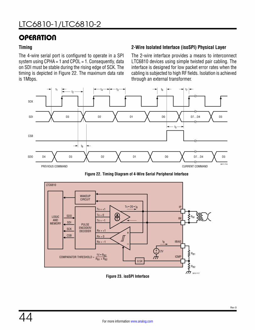
LTC6810-1/LTC6810-2
44Rev 0
For more information www.analog.com
OPERATIONTiming
The 4-wire serial port is configured to operate in a SPI system using CPHA = 1 and CPOL = 1. Consequently, data on SDI must be stable during the rising edge of SCK. The timing is depicted in Figure 22. The maximum data rate is 1Mbps.
2-Wire Isolated Interface (isoSPI) Physical Layer
The 2-wire interface provides a means to interconnect LTC6810 devices using simple twisted pair cabling. The interface is designed for low packet error rates when the cabling is subjected to high RF fields. Isolation is achieved through an external transformer.
68111 F16
SDI
SCK
D3 D2 D1 D0 D7…D4 D3
CURRENT COMMANDPREVIOUS COMMAND
t7
t8
t6
t5
SDO
CSB
D3D4 D2 D1 D0 D7…D4 D3
t1 t2t3t4
68101 F17
IMRM
IBIASIB
RB1ICMP
2V
IP
LOGICAND
MEMORY
Tx = +1Tx • 20 • IB
Tx = –1
SDO Tx = 0
PULSEENCODER/DECODER
SDI
SCK
CSB
WAKEUPCIRCUIT
LTC6810
+–
–
+
••
Rx = +1
Rx = –1
Rx = 0
RB2
COMPARATOR THRESHOLD = RB1 + RB2
1V • RB2
0.5X
Figure 22. Timing Diagram of 4-Wire Serial Peripheral Interface
Figure 23. isoSPI Interface
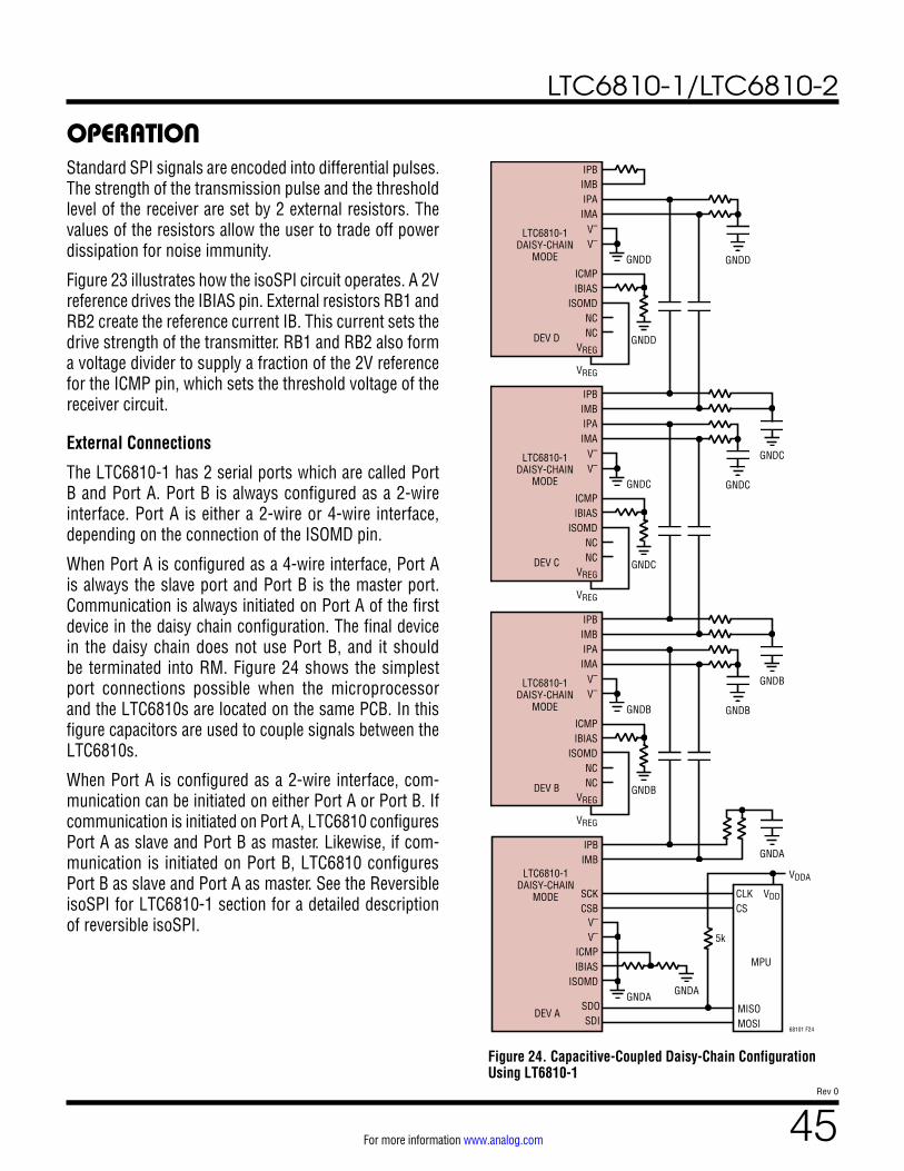
LTC6810-1/LTC6810-2
45Rev 0
For more information www.analog.com
OPERATIONStandard SPI signals are encoded into differential pulses. The strength of the transmission pulse and the threshold level of the receiver are set by 2 external resistors. The values of the resistors allow the user to trade off power dissipation for noise immunity.
Figure 23 illustrates how the isoSPI circuit operates. A 2V reference drives the IBIAS pin. External resistors RB1 and RB2 create the reference current IB. This current sets the drive strength of the transmitter. RB1 and RB2 also form a voltage divider to supply a fraction of the 2V reference for the ICMP pin, which sets the threshold voltage of the receiver circuit.
External Connections
The LTC6810-1 has 2 serial ports which are called Port B and Port A. Port B is always configured as a 2-wire interface. Port A is either a 2-wire or 4-wire interface, depending on the connection of the ISOMD pin.
When Port A is configured as a 4-wire interface, Port A is always the slave port and Port B is the master port. Communication is always initiated on Port A of the first device in the daisy chain configuration. The final device in the daisy chain does not use Port B, and it should be terminated into RM. Figure 24 shows the simplest port connections possible when the microprocessor and the LTC6810s are located on the same PCB. In this figure capacitors are used to couple signals between the LTC6810s.
When Port A is configured as a 2-wire interface, com-munication can be initiated on either Port A or Port B. If communication is initiated on Port A, LTC6810 configures Port A as slave and Port B as master. Likewise, if com-munication is initiated on Port B, LTC6810 configures Port B as slave and Port A as master. See the Reversible isoSPI for LTC6810-1 section for a detailed description of reversible isoSPI.
VREG
VREG
V–
V–
ICMPIBIAS
ISOMDNCNC
LTC6810-1DAISY-CHAIN
MODE
GNDD
GNDD
VREG
VREG
V–
V–
ICMPIBIAS
ISOMDNCNC
LTC6810-1DAISY-CHAIN
MODE
GNDB
GNDB
V–
V–
ICMPIBIAS
ISOMD
LTC6810-1DAISY-CHAIN
MODE
GNDA GNDA
GNDB
VREG
VREG
V–
V–
ICMPIBIAS
ISOMDNCNC
LTC6810-1DAISY-CHAIN
MODE
GNDC
GNDC
GNDA
MPU
68101 F24
GNDB
GNDC
GNDC
GNDD
IPBIMBIPAIMA
IPBIMB
SCKCSB
IPBIMBIPAIMA
VDDA
IPBIMBIPAIMA
CLKCS
MISOMOSI
VDD
5k
DEV D
DEV B
DEV C
DEV ASDOSDI
Figure 24. Capacitive-Coupled Daisy-Chain Configuration Using LT6810-1
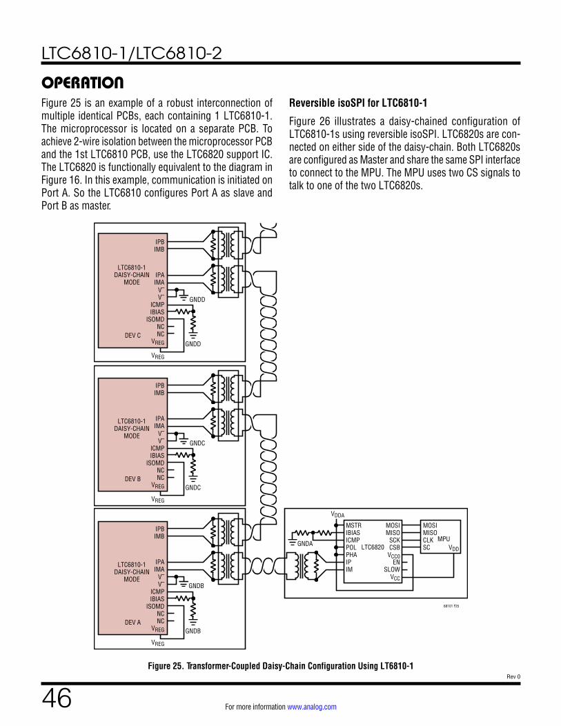
LTC6810-1/LTC6810-2
46Rev 0
For more information www.analog.com
OPERATIONFigure 25 is an example of a robust interconnection of multiple identical PCBs, each containing 1 LTC6810-1. The microprocessor is located on a separate PCB. To achieve 2-wire isolation between the microprocessor PCB and the 1st LTC6810 PCB, use the LTC6820 support IC. The LTC6820 is functionally equivalent to the diagram in Figure 16. In this example, communication is initiated on Port A. So the LTC6810 configures Port A as slave and Port B as master.
Reversible isoSPI for LTC6810-1
Figure 26 illustrates a daisy-chained configuration of LTC6810-1s using reversible isoSPI. LTC6820s are con-nected on either side of the daisy-chain. Both LTC6820s are configured as Master and share the same SPI interface to connect to the MPU. The MPU uses two CS signals to talk to one of the two LTC6820s.
LTC6820MPU
GNDA
IPBIMB
IPAIMA
VREG
VREG
ICMPIBIAS
ISOMDNCNC
GNDD
GNDD
68101 F25
LTC6810-1DAISY-CHAIN
MODE
DEV C
V–
V–
IPBIMB
IPAIMA
VREG
VREG
ICMPIBIAS
ISOMDNCNC
GNDC
GNDC
LTC6810-1DAISY-CHAIN
MODE
DEV B
V–
V–
IPBIMB
IPAIMA
VREG
VREG
ICMPIBIAS
ISOMDNCNC
GNDB
GNDB
LTC6810-1DAISY-CHAIN
MODE
DEV A
V–
V–
MSTRIBIASICMPPOLPHAIPIM
MOSIMISO
SCKCSB
VCC0EN
SLOWVCC
MOSIMISOCLKSC VDD
VDDA
Figure 25. Transformer-Coupled Daisy-Chain Configuration Using LT6810-1
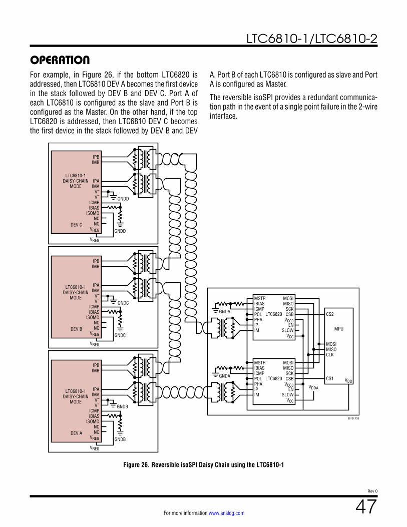
LTC6810-1/LTC6810-2
47Rev 0
For more information www.analog.com
OPERATIONFor example, in Figure 26, if the bottom LTC6820 is addressed, then LTC6810 DEV A becomes the first device in the stack followed by DEV B and DEV C. Port A of each LTC6810 is configured as the slave and Port B is configured as the Master. On the other hand, if the top LTC6820 is addressed, then LTC6810 DEV C becomes the first device in the stack followed by DEV B and DEV
A. Port B of each LTC6810 is configured as slave and Port A is configured as Master.
The reversible isoSPI provides a redundant communica-tion path in the event of a single point failure in the 2-wire interface.
GNDA LTC6820
GNDA LTC6820
MPU
IPBIMB
IPAIMA
VREG
VREG
ICMPIBIAS
ISOMDNCNC
GNDD
GNDD
68101 F26
LTC6810-1DAISY-CHAIN
MODE
DEV C
V–
V–
IPBIMB
IPAIMA
VREG
VREG
ICMPIBIAS
ISOMDNCNC
GNDC
GNDC
LTC6810-1DAISY-CHAIN
MODE
DEV B
V–
V–
IPBIMB
IPAIMA
VREG
VREG
ICMPIBIAS
ISOMDNCNC
GNDB
GNDB
LTC6810-1DAISY-CHAIN
MODE
DEV A
V–
V–
MSTRIBIASICMPPOLPHAIPIM
MOSIMISO
SCKCSB
VCC0EN
SLOWVCC
MSTRIBIASICMPPOLPHAIPIM
MOSIMISO
SCKCSB
VCC0EN
SLOWVCC
MOSIMISOCLK
VDDVDDA
CS1
CS2
Figure 26. Reversible isoSPI Daisy Chain using the LTC6810-1
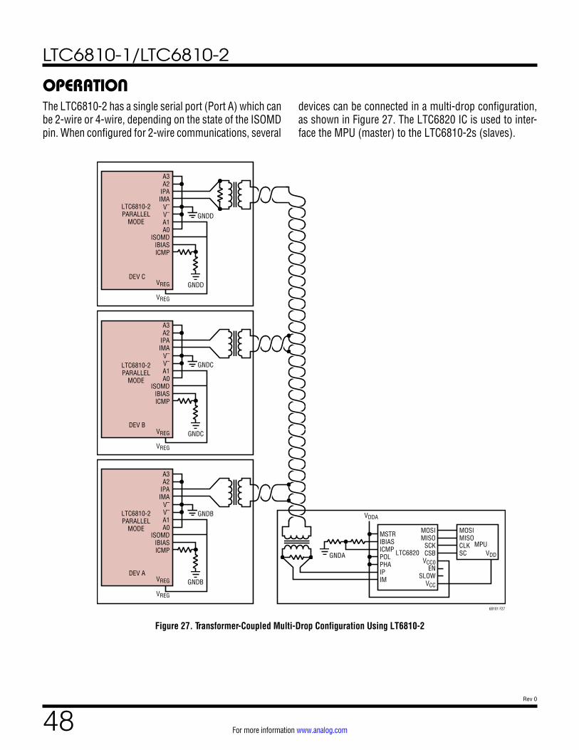
LTC6810-1/LTC6810-2
48Rev 0
For more information www.analog.com
OPERATIONThe LTC6810-2 has a single serial port (Port A) which can be 2-wire or 4-wire, depending on the state of the ISOMD pin. When configured for 2-wire communications, several
devices can be connected in a multi-drop configuration, as shown in Figure 27. The LTC6820 IC is used to inter-face the MPU (master) to the LTC6810-2s (slaves).
LTC6820MPU
GNDA
A3A2
IPAIMA
VREG
VREG
A1A0
ISOMDIBIASICMP
GNDD
GNDD
68101 F27
LTC6810-2PARALLEL
MODE
DEV C
V–
V–
LTC6810-2PARALLEL
MODE
DEV B
VREG
VREG
GNDB
LTC6810-2PARALLEL
MODE
DEV A
MSTRIBIASICMPPOLPHAIPIM
MOSIMISO
SCKCSB
VCC0EN
SLOWVCC
MOSIMISOCLKSC VDD
VDDA
A3A2
IPAIMA
VREG
VREG
A1A0
ISOMDIBIASICMP
GNDC
GNDCV–
V–
A3A2
IPAIMA
A1A0
ISOMDIBIASICMP
GNDBV–
V–
Figure 27. Transformer-Coupled Multi-Drop Configuration Using LT6810-2
LTC6810-1/LTC6810-2
49Rev 0
For more information www.analog.com
OPERATIONSelecting Bias Resistors
The isoSPI transmitter drive current and comparator volt-age threshold are set by a resistor divider (RBIAS = RB1 + RB2) between the IBIAS and V– pins. The divided voltage is connected to the ICMP pin, which sets the comparator threshold to ½ of this voltage (VICMP). When either isoSPI interface is enabled (not IDLE) IBIAS is held at 2V, causing a current IB to flow out of the IBIAS pin. The IP and IM pin drive currents are 20 • IB.
As an example, if divider resistor RB1 is 1.78kΩ and resis-tor RB2 is 200Ω (so that RBIAS = 2kΩ), then:
IB2V
RB1 RB21mA
IDRV = IIP = IIM = 20 • IB = 20mA
VICMP 2V •
RB2RB1 RB2
IB • RB2 422mV
VTCMP = 0.5 • VICMP = 211mV
In this example, the pulse drive current IDRV will be 20mA, and the receiver comparators will detect pulses with IP–IM amplitudes greater than ±211mV.
If the isolation barrier uses 1:1 transformers connected by a twisted pair and terminated with 100Ω resistors on each end, then the transmitted differential signal amplitude (±) will be:
VA IDRV •
RM2
1V
(This result ignores transformer and cable losses, which may reduce the amplitude.)
The adjustable signal amplitude allows the system to trade power consumption for communication robustness, and the adjustable comparator threshold allows the system to account for signal losses.
isoSPI Pulse Detail
Two LTC6810 devices can communicate by transmitting and receiving differential pulses back and forth through an isolation barrier. The transmitter can output three voltage levels: +VA, 0V, and –VA. A positive output results from IP sourcing current and IM sinking current across load resistor RM. A negative voltage is developed by IP sink-ing and IM sourcing. When both outputs are off, the load resistance forces the differential output to 0V.
To eliminate the DC signal component and enhance reli-ability, isoSPI pulses are defined as symmetric pulse pairs. A +1 pulse will be transmitted as a positive pulse followed by a negative pulse. A –1 pulse will be transmitted as a negative pulse followed by a positive pulse. The duration of each pulse is defined as t½PW, since each is half of the required symmetric pair (the total isoSPI pulse duration is 2 • t½PW).
Table 27. isoSPI Pulse Types
PULSE TYPEFIRST LEVEL
(t½PW)SECOND LEVEL
(t½PW) ENDING LEVEL
Long +1 +VA (150ns) –VA (150ns) 0V
Long –1 –VA (150ns) +VA (150ns) 0V
Short +1 +VA (50ns) –VA (50ns) 0V
Short –1 –VA (50ns) +VA (50ns) 0V
A host microcontroller does not have to generate isoSPI pulses to use this 2-wire interface. The first LTC6810 in the system can communicate to the microcontroller using the 4-wire SPI interface on its Port A, then daisy-chain to other LTC6810s using the 2-wire isoSPI interface on its Port B. Alternatively, the LTC6820 can be used to translate the SPI signals into isoSPI pulses.
When the LTC6810-1 is operation with Port A as a SPI (ISOMD = V–), the SPI detects one of four communication events: CSB falling, CSB rising, SCK rising with SDI = 0, and SCK rising with SDI = 1. Each event is converted into one of four pulse types for transmission to another daisy-chained LTC6810. Long pulses are used to transmit CSB changes and short pulses transmit data as explained in Table 28.

LTC6810-1/LTC6810-2
50Rev 0
For more information www.analog.com
OPERATIONTable 28. Port B (Master) isoSPI Port Function
COMMUNICATION EVENT (Port A SPI)
TRANSMITTED PULSE (Port B isoSPI)
CS Rising Long +1
CS Falling Long –1
SCK Rising Edge, SDI = 1 Short +1
SCK Rising Edge, SDI = 0 Short –1
On the other side of the isolation barrier (i.e. at the other end of the cable), the 2nd LTC6810 will have ISOMD = VREG. Its Port A operates as a slave isoSPI interface. It receives each transmitted pulse and reconstructs the SPI signals internally, as shown in Table 29. In addition, during a READ command this port may transmit return data pulses.
Table 29. Port A (Slave) isoSPI Port FunctionRECEIVED PULSE
(Port A isoSPI)INTERNAL SPI PORT
ACTIONRETURN PULSE
Long +1 Drive CS High None
Long –1 Drive CS Low Short –1 Pulse if Reading a 0 bit
(No Return Pulse if Not in READ Mode or if Reading a 1 bit)
Short +1 1. Set SDI = 1 2. Pulse SCK
Short –1 1. Set SDI = 0 2. Pulse SCK
The lower isoSPI port (slave) never transmits long (CSB) pulses. Furthermore, a slave isoSPI port will only trans-mit short –1 pulses, never a +1 pulse. The master port recognizes a null response as a logic 1. This allows for multiple slave devices on a single cable without risk of collisions (Multi-drop).
Figure 28. isoSPI Pulse Detail
+VA
–VA
+VA
–VA
+VTCMP
–VTCMP
VIP – VIM
+1 PULSE
tINV t1/2PW
+VTCMP
–VTCMP
VIP – VIM
t1/2PW
tINV t1/2PW
68101 F28
–1 PULSE
t1/2PW
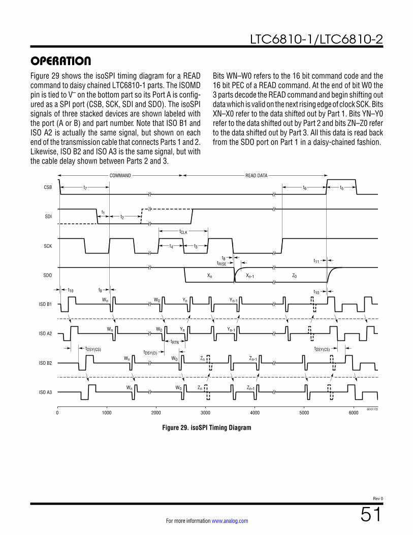
LTC6810-1/LTC6810-2
51Rev 0
For more information www.analog.com
OPERATIONFigure 29 shows the isoSPI timing diagram for a READ command to daisy chained LTC6810-1 parts. The ISOMD pin is tied to V– on the bottom part so its Port A is config-ured as a SPI port (CSB, SCK, SDI and SDO). The isoSPI signals of three stacked devices are shown labeled with the port (A or B) and part number. Note that ISO B1 and ISO A2 is actually the same signal, but shown on each end of the transmission cable that connects Parts 1 and 2. Likewise, ISO B2 and ISO A3 is the same signal, but with the cable delay shown between Parts 2 and 3.
Bits WN–W0 refers to the 16 bit command code and the 16 bit PEC of a READ command. At the end of bit W0 the 3 parts decode the READ command and begin shifting out data which is valid on the next rising edge of clock SCK. Bits XN–X0 refer to the data shifted out by Part 1. Bits YN–Y0 refer to the data shifted out by Part 2 and bits ZN–Z0 refer to the data shifted out by Part 3. All this data is read back from the SDO port on Part 1 in a daisy-chained fashion.
Figure 29. isoSPI Timing Diagram
68101 F29
SDI
SCK
SDO
CSB
ISO A2
ISO B2
ISO A3
ISO B1
READ DATACOMMAND
6000500040003000200010000
t7 t6 t5
tRTN
t11
t10
t2t1
tCLK
t4 t3
tRISE
tDSY(CS)
t8
t9
tDSY(CS)
Zn-1
Zn-1
Zn
Zn
W0
W0
Wn
Wn
Yn-1
Yn-1
Yn
Yn
W0
W0
Xn-1Xn Z0
Wn
Wn
tDSY(D)
t10
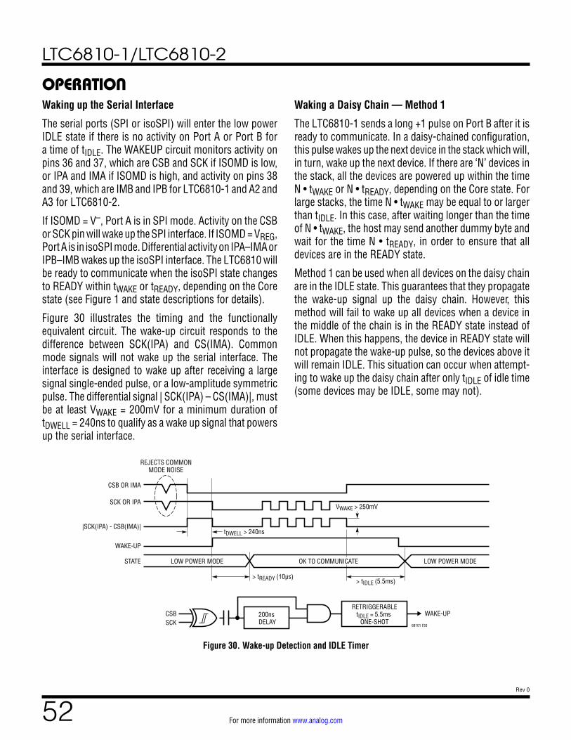
LTC6810-1/LTC6810-2
52Rev 0
For more information www.analog.com
OPERATIONWaking up the Serial Interface
The serial ports (SPI or isoSPI) will enter the low power IDLE state if there is no activity on Port A or Port B for a time of tIDLE. The WAKEUP circuit monitors activity on pins 36 and 37, which are CSB and SCK if ISOMD is low, or IPA and IMA if ISOMD is high, and activity on pins 38 and 39, which are IMB and IPB for LTC6810-1 and A2 and A3 for LTC6810-2.
If ISOMD = V–, Port A is in SPI mode. Activity on the CSB or SCK pin will wake up the SPI interface. If ISOMD = VREG, Port A is in isoSPI mode. Differential activity on IPA–IMA or IPB–IMB wakes up the isoSPI interface. The LTC6810 will be ready to communicate when the isoSPI state changes to READY within tWAKE or tREADY, depending on the Core state (see Figure 1 and state descriptions for details).
Figure 30 illustrates the timing and the functionally equivalent circuit. The wake-up circuit responds to the difference between SCK(IPA) and CS(IMA). Common mode signals will not wake up the serial interface. The interface is designed to wake up after receiving a large signal single-ended pulse, or a low-amplitude symmetric pulse. The differential signal | SCK(IPA) – CS(IMA)|, must be at least VWAKE = 200mV for a minimum duration of tDWELL = 240ns to qualify as a wake up signal that powers up the serial interface.
Waking a Daisy Chain — Method 1
The LTC6810-1 sends a long +1 pulse on Port B after it is ready to communicate. In a daisy-chained configuration, this pulse wakes up the next device in the stack which will, in turn, wake up the next device. If there are ‘N’ devices in the stack, all the devices are powered up within the time N • tWAKE or N • tREADY, depending on the Core state. For large stacks, the time N • tWAKE may be equal to or larger than tIDLE. In this case, after waiting longer than the time of N • tWAKE, the host may send another dummy byte and wait for the time N • tREADY, in order to ensure that all devices are in the READY state.
Method 1 can be used when all devices on the daisy chain are in the IDLE state. This guarantees that they propagate the wake-up signal up the daisy chain. However, this method will fail to wake up all devices when a device in the middle of the chain is in the READY state instead of IDLE. When this happens, the device in READY state will not propagate the wake-up pulse, so the devices above it will remain IDLE. This situation can occur when attempt-ing to wake up the daisy chain after only tIDLE of idle time (some devices may be IDLE, some may not).
Figure 30. Wake-up Detection and IDLE Timer
68101 F30
CSB OR IMA
SCK OR IPA
|SCK(IPA) - CSB(IMA)|
WAKE-UP
STATE
REJECTS COMMONMODE NOISE
WAKE-UPCSBSCK
LOW POWER MODE
> tIDLE (5.5ms)> tREADY (10µs)
tDWELL > 240ns
VWAKE > 250mV
LOW POWER MODE OK TO COMMUNICATE
200ns DELAY
RETRIGGERABLEtIDLE = 5.5ms
ONE-SHOT
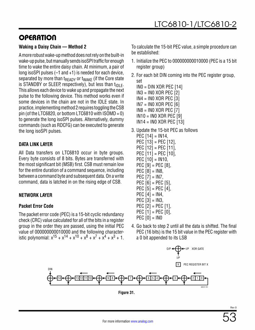
LTC6810-1/LTC6810-2
53Rev 0
For more information www.analog.com
OPERATIONWaking a Daisy Chain — Method 2
A more robust wake-up method does not rely on the built-in wake-up pulse, but manually sends isoSPI traffic for enough time to wake the entire daisy chain. At minimum, a pair of long isoSPI pulses (–1 and +1) is needed for each device, separated by more than tREADY or tWAKE (if the Core state is STANDBY or SLEEP, respectively), but less than tIDLE. This allows each device to wake up and propagate the next pulse to the following device. This method works even if some devices in the chain are not in the IDLE state. In practice, implementing method 2 requires toggling the CSB pin (of the LTC6820, or bottom LTC6810 with ISOMD = 0) to generate the long isoSPI pulses. Alternatively, dummy commands (such as RDCFG) can be executed to generate the long isoSPI pulses.
DATA LINK LAYER
All Data transfers on LTC6810 occur in byte groups. Every byte consists of 8 bits. Bytes are transferred with the most significant bit (MSB) first. CSB must remain low for the entire duration of a command sequence, including between a command byte and subsequent data. On a write command, data is latched in on the rising edge of CSB.
NETWORK LAYER
Packet Error Code
The packet error code (PEC) is a 15-bit cyclic redundancy check (CRC) value calculated for all of the bits in a register group in the order they are passed, using the initial PEC value of 000000000010000 and the following character-istic polynomial: x15 + x14 + x10 + x8 + x7 + x4 + x3 + 1.
To calculate the 15-bit PEC value, a simple procedure can be established:
1. Initialize the PEC to 000000000010000 (PEC is a 15 bit register group)
2. For each bit DIN coming into the PEC register group, set IN0 = DIN XOR PEC [14] IN3 = IN0 XOR PEC [2] IN4 = IN0 XOR PEC [3] IN7 = IN0 XOR PEC [6] IN8 = IN0 XOR PEC [7] IN10 = IN0 XOR PEC [9] IN14 = IN0 XOR PEC [13]
3. Update the 15-bit PEC as follows PEC [14] = IN14, PEC [13] = PEC [12], PEC [12] = PEC [11], PEC [11] = PEC [10], PEC [10] = IN10, PEC [9] = PEC [8], PEC [8] = IN8, PEC [7] = IN7, PEC [6] = PEC [5], PEC [5] = PEC [4], PEC [4] = IN4, PEC [3] = IN3, PEC [2] = PEC [1], PEC [1] = PEC [0], PEC [0] = IN0
4. Go back to step 2 until all the data is shifted. The final PEC (16 bits) is the 15 bit value in the PEC register with a 0 bit appended to its LSB
Figure 31. 68101 F31
DIN
I/P
O/P I/P
PEC REGISTER BIT X
XOR GATE
X
012345678914 10111213
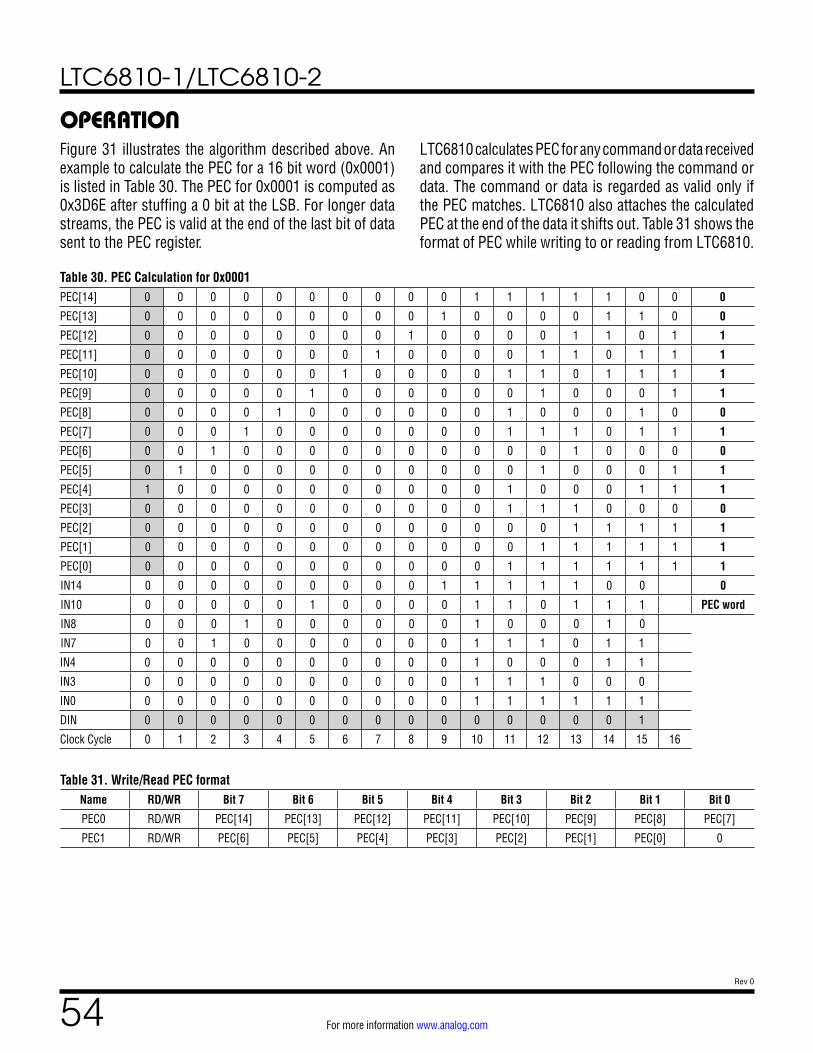
LTC6810-1/LTC6810-2
54Rev 0
For more information www.analog.com
OPERATION
Table 30. PEC Calculation for 0x0001PEC[14] 0 0 0 0 0 0 0 0 0 0 1 1 1 1 1 0 0 0
PEC[13] 0 0 0 0 0 0 0 0 0 1 0 0 0 0 1 1 0 0
PEC[12] 0 0 0 0 0 0 0 0 1 0 0 0 0 1 1 0 1 1
PEC[11] 0 0 0 0 0 0 0 1 0 0 0 0 1 1 0 1 1 1
PEC[10] 0 0 0 0 0 0 1 0 0 0 0 1 1 0 1 1 1 1
PEC[9] 0 0 0 0 0 1 0 0 0 0 0 0 1 0 0 0 1 1
PEC[8] 0 0 0 0 1 0 0 0 0 0 0 1 0 0 0 1 0 0
PEC[7] 0 0 0 1 0 0 0 0 0 0 0 1 1 1 0 1 1 1
PEC[6] 0 0 1 0 0 0 0 0 0 0 0 0 0 1 0 0 0 0
PEC[5] 0 1 0 0 0 0 0 0 0 0 0 0 1 0 0 0 1 1
PEC[4] 1 0 0 0 0 0 0 0 0 0 0 1 0 0 0 1 1 1
PEC[3] 0 0 0 0 0 0 0 0 0 0 0 1 1 1 0 0 0 0
PEC[2] 0 0 0 0 0 0 0 0 0 0 0 0 0 1 1 1 1 1
PEC[1] 0 0 0 0 0 0 0 0 0 0 0 0 1 1 1 1 1 1
PEC[0] 0 0 0 0 0 0 0 0 0 0 0 1 1 1 1 1 1 1
IN14 0 0 0 0 0 0 0 0 0 1 1 1 1 1 0 0 0
IN10 0 0 0 0 0 1 0 0 0 0 1 1 0 1 1 1 PEC word
IN8 0 0 0 1 0 0 0 0 0 0 1 0 0 0 1 0
IN7 0 0 1 0 0 0 0 0 0 0 1 1 1 0 1 1
IN4 0 0 0 0 0 0 0 0 0 0 1 0 0 0 1 1
IN3 0 0 0 0 0 0 0 0 0 0 1 1 1 0 0 0
IN0 0 0 0 0 0 0 0 0 0 0 1 1 1 1 1 1
DIN 0 0 0 0 0 0 0 0 0 0 0 0 0 0 0 1
Clock Cycle 0 1 2 3 4 5 6 7 8 9 10 11 12 13 14 15 16
Table 31. Write/Read PEC formatName RD/WR Bit 7 Bit 6 Bit 5 Bit 4 Bit 3 Bit 2 Bit 1 Bit 0
PEC0 RD/WR PEC[14] PEC[13] PEC[12] PEC[11] PEC[10] PEC[9] PEC[8] PEC[7]
PEC1 RD/WR PEC[6] PEC[5] PEC[4] PEC[3] PEC[2] PEC[1] PEC[0] 0
Figure 31 illustrates the algorithm described above. An example to calculate the PEC for a 16 bit word (0x0001) is listed in Table 30. The PEC for 0x0001 is computed as 0x3D6E after stuffing a 0 bit at the LSB. For longer data streams, the PEC is valid at the end of the last bit of data sent to the PEC register.
LTC6810 calculates PEC for any command or data received and compares it with the PEC following the command or data. The command or data is regarded as valid only if the PEC matches. LTC6810 also attaches the calculated PEC at the end of the data it shifts out. Table 31 shows the format of PEC while writing to or reading from LTC6810.
LTC6810-1/LTC6810-2
55Rev 0
For more information www.analog.com
OPERATIONWhile writing any command to LTC6810, the command bytes CMD0 and CMD1 (see Table 38 and Table 39) and the PEC bytes PEC0 and PEC1 are sent on Port A in the following order:
CMD0, CMD1, PEC0, PEC1
After a broadcast write command to daisy chained LTC6810-1 devices, data is sent to each device followed by the PEC. For example, when writing the Configuration Register Group to two daisy-chained devices (primary device P, stacked device S), the data will be sent to the primary device on its slave port in the following order:
CFGR0(S), …, CFGR5(S), PEC0(S), PEC1(S), CFGR0(P), …, CFGR5(P), PEC0(P), PEC1(P)
After a read command for daisy chained devices, each device shifts out its data and the PEC that it computed for its data on its slave port followed by the data received on its master port. For example, when reading Status Register Group B from two daisy-chained devices (primary device P, stacked device S), the primary device sends out data on its slave port in the following order:
STBR0(P), …, STBR5(P), PEC0(P), PEC1(P), STBR0(S), …, STBR5(S), PEC0(S), PEC1(S)
Address Commands (LTC6810-2 Only)
An address command is one in which only the addressed device on the bus responds. Address commands are used only with LTC6810-2 parts. All commands are compatible with addressing. See the Bus Protocols section for Address command format.
Broadcast Commands (LTC6810-1 or LTC6810-2)
A broadcast command is one to which all devices on the bus will respond, regardless of device address. This command can be used with LTC6810-1 and LTC6810-2 parts. See the Bus Protocols section for Broadcast com-mand format. With broadcast commands all devices can be sent commands simultaneously.
In parallel (LTC6810-2) configurations, broadcast com-mands are useful for initiating ADC conversions or for sending write commands when all parts are being written with the same data. The polling function (automatic at the end of ADC commands, or manual using the PLADC com-mand) can also be used with broadcast commands, but not with parallel isoSPI devices. Likewise, broadcast read commands should not be used in the parallel configuration (either SPI or isoSPI).
Daisy-chained (LTC6810-1) configurations support broad-cast commands only, because they have no addressing. All devices in the chain receive the command bytes simul-taneously. For example, to initiate ADC conversions in a stack of devices, a single ADCV command is sent, and all devices will start conversions at the same time. For read and write commands, a single command is sent, and then the stacked devices effectively turn into a cascaded shift register, in which data is shifted through each device to the next higher (on a write) or the next lower (on a read) device in the stack. See the Serial Interface Overview section.
Polling Methods
The simplest method to determine ADC completion is for the controller to start an ADC conversion and wait for the specified conversion time to pass before reading the results. Both LTC6810-1 and LTC6810-2 also allow polling to determine ADC completion.
In parallel configurations that communicate in SPI mode (ISOMD pin tied low), there are two methods of polling. The first method is to hold CSBI low after an ADC con-version command is sent. After entering a conversion command, the SDO line is driven low when the device is busy performing conversions. SDO is pulled high when the device completes conversions. However, the SDO will also go back high when CSBI goes high even if the device has not completed the conversion (Figure 32). An addressed device drives the SDO line based on its status alone. A problem with this method is that the controller is not free to do other serial communication while waiting for ADC conversions to complete.
LTC6810-1/LTC6810-2
56Rev 0
For more information www.analog.com
OPERATIONThe next method overcomes this limitation. The controller can send an ADC start command, perform other tasks, and then send a poll ADC converter status (PLADC) command to determine the status of the ADC conversions (Figure 33). After entering the PLADC command, SDO will go low if the device is busy performing conversions. SDO is pulled high at the end of conversions. However, the SDO will also go high when CSBI goes high even if the device has not completed the conversion.
In parallel configurations that communicate in isoSPI mode, the low side port transmits a data pulse only in response to a master isoSPI pulse received by it. So, after enter-ing the command in either method of polling described above, isoSPI data pulses are sent to the part to update the conversion status. These pulses can be sent using LTC6820 by simply clocking its SCK pin. In response to this pulse, the device sends back a low isoSPI pulse if it is still busy performing conversions or a high data pulse if it has completed the conversions. If a CSB high isoSPI pulse is sent to the device, it exits the polling command.
Figure 32. SDO Polling After an ADC Conversion Command (Parallel Configuration)
Figure 33. SDO Polling Using PLADC Command (Parallel Configuration)
68101 F32
SDI
SCK
tCYCLE
SDO
CSB
MSB(CMD) LSB(PEC)BIT 14(CMD)
68101 F33
SDI
SCK
SDO
CSB
MSB(CMD) LSB(PEC)
CONVERSION DONE
BIT 14(CMD)

LTC6810-1/LTC6810-2
57Rev 0
For more information www.analog.com
OPERATIONIn a daisy-chained configuration of N stacked devices, the same two polling methods can be used. If the bottom device communicates in SPI mode, the SDO of the bot-tom device indicates the conversion status of the entire stack (i.e. SDO will remain low until all the devices in the stack have completed conversions). In the first method of polling, after an ADC conversion command is sent, clock pulses are sent on SCK while keeping CSB low. The SDO status becomes valid only at the end of N clock pulses on SCK and gets updated for every clock pulse that follows (Figure 34). In the second method, the PLADC command is sent followed by clock pulses on SCK while keeping
CSBI low. Similar to the first method, the SDO status is valid only after N clock cycles on SCKI and gets updated after every clock cycle that follows (Figure 35).
If the bottom device communicates in isoSPI mode, isoSPI data pulses are sent to the device to update the conversion status. Using LTC6820, this can be achieved by just clock-ing its SCK pin. The conversion status is valid only after the bottom LTC6810 device receives N isoSPI data pulses and the status gets updated for every isoSPI data pulse that follows. The device returns a low data pulse if any of the devices in the stack is busy performing conversions and returns a high data pulse if all the devices are free.
Figure 34.
Figure 35.
68101 F34
SDI
SCK
tCYCLE (ALL DEVICES)
SDO
CSB
MSB(CMD) LSB(PEC)
1 2 N
68101 F35
SDI
SCK
SDO
CSB
MSB(CMD) LSB(PEC)
1 2 N
CONVERSION DONE

LTC6810-1/LTC6810-2
58Rev 0
For more information www.analog.com
OPERATIONCommand Format: The formats for the broadcast and address commands are shown in Table 38 and Table 39 respectively. The 11 bit command code CC[10:0] is the same for a broadcast or an address command. A list of all the command codes is shown in Table 40. A broadcast command has a value 0 for CMD0[7] through CMD0[3]. An address command has a value 1 for CMD0[7] fol-lowed by the 4 bit address of the device (a3, a2, a1, a0) in bits CMD0[6:3]. An addressed device will respond to an address command only if the physical address of the device on pins A3 to A0 match the address specified in the address command. The PEC for broadcast and address commands must be computed on the entire 16 bit command (CMD0 and CMD1).
Bus Protocols
Protocol Format: The protocol formats for both broadcast and address commands are depicted in Table 33 through Table 37. Table 32 is the key for reading the protocol diagrams.
Table 32. Protocol KeyCMD0 Command Byte 0 (See Table 38 and Table 39)
CMD1 Command Byte 1 (See Table 38 and Table 39)
PEC0 Packet Error Code Byte 0 (See Table 31)
PEC1 Packet Error Code Byte 1 (See Table 31)
N Number of Bytes
… Continuation of Protocol
Master to Slave
Slave to Master
Table 33. Broadcast/Address Poll Command8 8 8 8
CMD0 CMD1 PEC0 PEC1 Poll Data
Table 34. Broadcast Write Command8 8 8 8 8 8 8 8 8 8
CMD0 CMD1 PEC0 PEC1 Data Byte Low … Data Byte High PEC0 PEC1 Shift Byte 1 … Shift Byte n
Table 35. Address Write Command8 8 8 8 8 8 8 8
CMD0 CMD1 PEC0 PEC1 Data Byte Low … Data Byte High PEC0 PEC1
Table 36. Broadcast Read Command8 8 8 8 8 8 8 8 8 8
CMD0 CMD1 PEC0 PEC1 Data Byte Low … Data Byte High PEC0 PEC1 Shift Byte 1 … Shift Byte n
Table 37. Address Read Command8 8 8 8 8 8 8 8
CMD0 CMD1 PEC0 PEC1 Data Byte Low … Data Byte High PEC0 PEC1
Table 38. Broadcast Command FormatNAME RD/WR BIT 7 BIT 6 BIT 5 BIT 4 BIT 3 BIT 2 BIT 1 BIT 0
CMD0 WR 0 0 0 0 0 CC[10] CC[9] CC[8]
CMD1 WR CC[7] CC[6] CC[5] CC[4] CC[3] CC[2] CC[1] CC[0]
Table 39. Address Command FormatNAME RD/WR BIT 7 BIT 6 BIT 5 BIT 4 BIT 3 BIT 2 BIT 1 BIT 0
CMD0 WR 1 a3* a2* a1* a0* CC[10] CC[9] CC[8]
CMD1 WR CC[7] CC[6] CC[5] CC[4] CC[3] CC[2] CC[1] CC[0]
*ax is Address Bit x
LTC6810-1/LTC6810-2
59Rev 0
For more information www.analog.com
OPERATION
Table 40. Command CodesCOMMAND DESCRIPTION NAME CC[10:0] — COMMAND CODE
10 9 8 7 6 5 4 3 2 1 0
Write Configuration Register Group
WRCFG 0 0 0 0 0 0 0 0 0 0 1
Read Configuration Register Group
RDCFG 0 0 0 0 0 0 0 0 0 1 0
Write Control Register Group (PWM and S)
WRSCTRL* 0 0 0 0 0 0 1 0 1 0 0
Read Control Register Group (PWM and S)
RDSCTRL* 0 0 0 0 0 0 1 0 1 1 0
Write PWM Register Group (PWM and S)
WRPWM* 0 0 0 0 0 1 0 0 0 0 0
Read PWM Register Group (PWM and S)
RDPWM* 0 0 0 0 0 1 0 0 0 1 0
Read Cell Voltage Register Group A
RDCVA 0 0 0 0 0 0 0 0 1 0 0
Read Cell Voltage Register Group B
RDCVB 0 0 0 0 0 0 0 0 1 1 0
Read S Voltage Register Group A
RDSA 0 0 0 0 0 0 0 1 0 0 0
Read S Voltage Register Group B
RDSB 0 0 0 0 0 0 0 1 0 1 0
Read Auxiliary Register Group A
RDAUXA 0 0 0 0 0 0 0 1 1 0 0
Read Auxiliary Register Group B
RDAUXB 0 0 0 0 0 0 0 1 1 1 0
Read Status Register Group A
RDSTATA 0 0 0 0 0 0 1 0 0 0 0
Read Status Register Group B
RDSTATB 0 0 0 0 0 0 1 0 0 1 0
Read Serial ID Register Group
RDSID 0 0 0 0 0 1 0 1 1 0 0
Start Cell Voltage ADC Conversion and Poll Status
ADCV 0 1 MD[1] MD[0] 1 1 DCP 0 CH[2] CH[1] CH[0]
Start Open Wire ADC Conversion and Poll Status
ADOW 0 1 MD[1] MD[0] PUP 1 DCP 1 CH[2] CH[1] CH[0]
Start Self-Test Cell Voltage Conversion and Poll Status
CVST 0 1 MD[1] MD[0] ST[1] ST[0] 0 0 1 1 1
Start GPIOs/Cell 0/REF2 ADC Conversion and Poll Status
ADAX 1 0 MD[1] MD[0] 1 1 0 0 CHG[2] CHG[1] CHG[0]
Start GPIOs/Cell 0/REF2 ADC Conversion with Digital Redundancy and Poll Status
ADAXD 1 0 MD[1] MD[0] 0 0 0 0 CHG[2] CHG[1] CHG[0]
Commands
Table 40 lists all the commands and its options for both LTC6810-1 and LTC6810-2.
LTC6810-1/LTC6810-2
60Rev 0
For more information www.analog.com
OPERATIONCOMMAND DESCRIPTION NAME CC[10:0] — COMMAND CODE
10 9 8 7 6 5 4 3 2 1 0
Start GPIOs/Cell 0/REF2 ADC Open Wire Conversion
AXOW 1 0 MD[1] MD[0] PUP 0 1 0 CHG[2] CHG[1] CHG[0]
Start Self-Test GPIOs/Cell 0/REF2 Conversion and Poll Status
AXST 1 0 MD[1] MD[0] ST[1] ST[0] 0 0 1 1 1
Start Status Group ADC Conversion and Poll Status
ADSTAT 1 0 MD[1] MD[0] 1 1 0 1 CHST[2] CHST[1] CHST[0]
Start Status Group ADC Conversion with Digital Redundancy and Poll Status
ADSTATD 1 0 MD[1] MD[0] 0 0 0 1 CHST[2] CHST[1] CHST[0]
Start Self-Test Status Group Conversion and Poll Status
STATST 1 0 MD[1] MD[0] ST[1] ST[0] 0 1 1 1 1
Start Combined Cell Voltage and Cell 0, GPIO1 Conversion and Poll Status
ADCVAX 1 0 MD[1] MD[0] 1 1 DCP 1 1 1 1
Start Combined Cell Voltage and SC Conversion and Poll Status
ADCVSOC 1 0 MD[1] MD[0] 1 1 DCP 0 1 1 1
Clear Cell Voltage Register Group
CLRCELL 1 1 1 0 0 0 1 0 0 0 1
Clear Auxiliary Register Group
CLRAUX 1 1 1 0 0 0 1 0 0 1 0
Clear Status Register Group CLRSTAT 1 1 1 0 0 0 1 0 0 1 1
Poll ADC Conversion Status PLADC 1 1 1 0 0 0 1 0 1 0 0
Diagnose MUX and Poll Status
DIAGN 1 1 1 0 0 0 1 0 1 0 1
Write COMM Register Group
WRCOMM 1 1 1 0 0 1 0 0 0 0 1
Read COMM Register Group
RDCOMM 1 1 1 0 0 1 0 0 0 1 0
Start I2C/SPI Communication STCOMM 1 1 1 0 0 1 0 0 0 1 1
Mute Discharge MUTE 0 0 0 0 0 1 0 1 0 0 0
Unmute Discharge UNMUTE 0 0 0 0 0 1 0 1 0 0 1
*The WRSCTRL and WRPWM and RDSCTRL and RDPWM commands all access the same PWM Register Group. The WRSCTRL and RDSCTRL commands are provided for compatibility with other LTC681x devices in a daisy-chain.
Table 41. Command Bit DescriptionsNAME DESCRIPTION VALUES
MD[1:0] ADC Mode
MD ADCOPT(CFGR0[0]) = 0 ADCOPT (CFGR0[0]) = 1
00 422Hz Mode 1kHz Mode
01 27 kHz Mode (Fast) 14 kHz Mode
10 7 kHz Mode (Normal) 3 kHz Mode
11 26 Hz Mode (Filtered) 2 kHz Mode
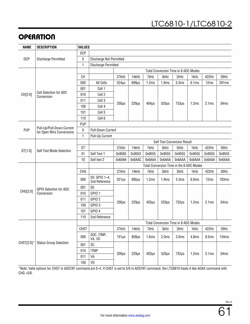
LTC6810-1/LTC6810-2
61Rev 0
For more information www.analog.com
OPERATIONNAME DESCRIPTION VALUES
DCP Discharge Permitted
DCP
0 Discharge Not Permitted
1 Discharge Permitted
CH[2:0] Cell Selection for ADC Conversion
Total Conversion Time in 8 ADC Modes
CH 27kHz 14kHz 7kHz 3kHz 2kHz 1kHz 422Hz 26Hz
000 All Cells 524µs 699µs 1.2ms 1.9ms 3.3ms 6.1ms 12ms 201ms
001 Cell 1
200µs 229µs 404µs 520µs 753µs 1.2ms 2.1ms 34ms
010 Cell 2
011 Cell 3
100 Cell 4
101 Cell 5
110 Cell 6
PUP Pull-Up/Pull-Down Current for Open Wire Conversions
PUP
0 Pull-Down Current
1 Pull-Up Current
ST[1:0] Self Test Mode Selection
Self Test Conversion Result
ST 27kHz 14kHz 7kHz 3kHz 2kHz 1kHz 422Hz 26Hz
01 Self Test 1 0x9565 0x9553 0x9555 0x9555 0x9555 0x9555 0x9555 0x9555
10 Self test 2 0x6A9A 0x6AAC 0x6AAA 0x6AAA 0x6AAA 0x6AAA 0x6AAA 0x6AAA
CHG[2:0] GPIO Selection for ADC Conversion
Total Conversion Time in the 8 ADC Modes
CHG 27kHz 14kHz 7kHz 3kHz 2kHz 1kHz 422Hz 26Hz
000 S0, GPIO 1–4, 2nd Reference 521µs 695µs 1.2ms 1.9ms 3.3ms 6.0ms 12ms 183ms
001 S0
200µs 229µs 403µs 520µs 752µs 1.2ms 2.1ms 34ms
010 GPIO 1
011 GPIO 2
100 GPIO 3
101 GPIO 4
110 2nd Reference
CHST[2:0]* Status Group Selection
Total Conversion Time in 8 ADC Modes
CHST 27kHz 14kHz 7kHz 3kHz 2kHz 1kHz 422Hz 26Hz
000 SOC, ITMP, VA, VD 741µs 858µs 1.6ms 2.0ms 3.0ms 4.8ms 8.5ms 134ms
001 SC
200µs 229µs 403µs 520µs 752µs 1.2ms 2.1ms 34ms010 ITMP
011 VA
100 VD
*Note: Valid options for CHST in ADSTAT command are 0–4. If CHST is set to 5/6 in ADSTAT command, the LTC6810 treats it like ADAX command with CHG =5/6.
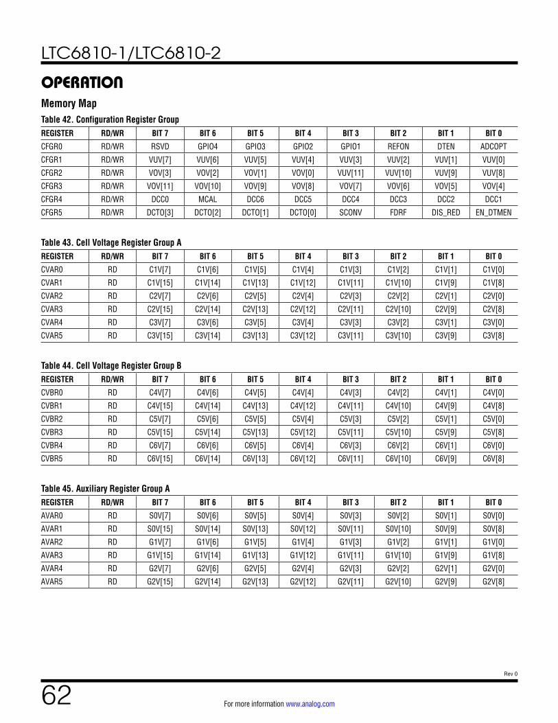
LTC6810-1/LTC6810-2
62Rev 0
For more information www.analog.com
OPERATIONMemory MapTable 42. Configuration Register GroupREGISTER RD/WR BIT 7 BIT 6 BIT 5 BIT 4 BIT 3 BIT 2 BIT 1 BIT 0
CFGR0 RD/WR RSVD GPIO4 GPIO3 GPIO2 GPIO1 REFON DTEN ADCOPT
CFGR1 RD/WR VUV[7] VUV[6] VUV[5] VUV[4] VUV[3] VUV[2] VUV[1] VUV[0]
CFGR2 RD/WR VOV[3] VOV[2] VOV[1] VOV[0] VUV[11] VUV[10] VUV[9] VUV[8]
CFGR3 RD/WR VOV[11] VOV[10] VOV[9] VOV[8] VOV[7] VOV[6] VOV[5] VOV[4]
CFGR4 RD/WR DCC0 MCAL DCC6 DCC5 DCC4 DCC3 DCC2 DCC1
CFGR5 RD/WR DCTO[3] DCTO[2] DCTO[1] DCTO[0] SCONV FDRF DIS_RED EN_DTMEN
Table 43. Cell Voltage Register Group AREGISTER RD/WR BIT 7 BIT 6 BIT 5 BIT 4 BIT 3 BIT 2 BIT 1 BIT 0
CVAR0 RD C1V[7] C1V[6] C1V[5] C1V[4] C1V[3] C1V[2] C1V[1] C1V[0]
CVAR1 RD C1V[15] C1V[14] C1V[13] C1V[12] C1V[11] C1V[10] C1V[9] C1V[8]
CVAR2 RD C2V[7] C2V[6] C2V[5] C2V[4] C2V[3] C2V[2] C2V[1] C2V[0]
CVAR3 RD C2V[15] C2V[14] C2V[13] C2V[12] C2V[11] C2V[10] C2V[9] C2V[8]
CVAR4 RD C3V[7] C3V[6] C3V[5] C3V[4] C3V[3] C3V[2] C3V[1] C3V[0]
CVAR5 RD C3V[15] C3V[14] C3V[13] C3V[12] C3V[11] C3V[10] C3V[9] C3V[8]
Table 44. Cell Voltage Register Group BREGISTER RD/WR BIT 7 BIT 6 BIT 5 BIT 4 BIT 3 BIT 2 BIT 1 BIT 0
CVBR0 RD C4V[7] C4V[6] C4V[5] C4V[4] C4V[3] C4V[2] C4V[1] C4V[0]
CVBR1 RD C4V[15] C4V[14] C4V[13] C4V[12] C4V[11] C4V[10] C4V[9] C4V[8]
CVBR2 RD C5V[7] C5V[6] C5V[5] C5V[4] C5V[3] C5V[2] C5V[1] C5V[0]
CVBR3 RD C5V[15] C5V[14] C5V[13] C5V[12] C5V[11] C5V[10] C5V[9] C5V[8]
CVBR4 RD C6V[7] C6V[6] C6V[5] C6V[4] C6V[3] C6V[2] C6V[1] C6V[0]
CVBR5 RD C6V[15] C6V[14] C6V[13] C6V[12] C6V[11] C6V[10] C6V[9] C6V[8]
Table 45. Auxiliary Register Group AREGISTER RD/WR BIT 7 BIT 6 BIT 5 BIT 4 BIT 3 BIT 2 BIT 1 BIT 0
AVAR0 RD S0V[7] S0V[6] S0V[5] S0V[4] S0V[3] S0V[2] S0V[1] S0V[0]
AVAR1 RD S0V[15] S0V[14] S0V[13] S0V[12] S0V[11] S0V[10] S0V[9] S0V[8]
AVAR2 RD G1V[7] G1V[6] G1V[5] G1V[4] G1V[3] G1V[2] G1V[1] G1V[0]
AVAR3 RD G1V[15] G1V[14] G1V[13] G1V[12] G1V[11] G1V[10] G1V[9] G1V[8]
AVAR4 RD G2V[7] G2V[6] G2V[5] G2V[4] G2V[3] G2V[2] G2V[1] G2V[0]
AVAR5 RD G2V[15] G2V[14] G2V[13] G2V[12] G2V[11] G2V[10] G2V[9] G2V[8]
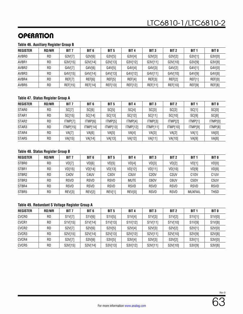
LTC6810-1/LTC6810-2
63Rev 0
For more information www.analog.com
OPERATIONTable 46. Auxiliary Register Group BREGISTER RD/WR BIT 7 BIT 6 BIT 5 BIT 4 BIT 3 BIT 2 BIT 1 BIT 0
AVBR0 RD G3V[7] G3V[6] G3V[5] G3V[4] G3V[3] G3V[2] G3V[1] G3V[0]
AVBR1 RD G3V[15] G3V[14] G3V[13] G3V[12] G3V[11] G3V[10] G3V[9] G3V[8]
AVBR2 RD G4V[7] G4V[6] G4V[5] G4V[4] G4V[3] G4V[2] G4V[1] G4V[0]
AVBR3 RD G4V[15] G4V[14] G4V[13] G4V[12] G4V[11] G4V[10] G4V[9] G4V[8]
AVBR4 RD REF[7] REF[6] REF[5] REF[4] REF[3] REF[2] REF[1] REF[0]
AVBR5 RD REF[15] REF[14] REF[13] REF[12] REF[11] REF[10] REF[9] REF[8]
Table 47. Status Register Group AREGISTER RD/WR BIT 7 BIT 6 BIT 5 BIT 4 BIT 3 BIT 2 BIT 1 BIT 0
STAR0 RD SC[7] SC[6] SC[5] SC[4] SC[3] SC[2] SC[1] SC[0]
STAR1 RD SC[15] SC[14] SC[13] SC[12] SC[11] SC[10] SC[9] SC[8]
STAR2 RD ITMP[7] ITMP[6] ITMP[5] ITMP[4] ITMP[3] ITMP[2] ITMP[1] ITMP[0]
STAR3 RD ITMP[15] ITMP[14] ITMP[13] ITMP[12] ITMP[11] ITMP[10] ITMP[9] ITMP[8]
STAR4 RD VA[7] VA[6] VA[5] VA[4] VA[3] VA[2] VA[1] VA[0]
STAR5 RD VA[15] VA[14] VA[13] VA[12] VA[11] VA[10] VA[9] VA[8]
Table 48. Status Register Group BREGISTER RD/WR BIT 7 BIT 6 BIT 5 BIT 4 BIT 3 BIT 2 BIT 1 BIT 0
STBR0 RD VD[7] VD[6] VD[5] VD[4] VD[3] VD[2] VD[1] VD[0]
STBR1 RD VD[15] VD[14] VD[13] VD[12] VD[11] VD[10] VD[9] VD[8]
STBR2 RD C4OV C4UV C3OV C3UV C2OV C2UV C1OV C1UV
STBR3 RD RSVD RSVD RSVD MUTE C6OV C6UV C5OV C5UV
STBR4 RD RSVD RSVD RSVD RSVD RSVD RSVD RSVD RSVD
STBR5 RD REV[3] REV[2] REV[1] REV[0] RSVD RSVD MUXFAIL THSD
Table 49. Redundant S Voltage Register Group AREGISTER RD/WR BIT 7 BIT 6 BIT 5 BIT 4 BIT 3 BIT 2 BIT 1 BIT 0
CVCR0 RD S1V[7] S1V[6] S1V[5] S1V[4] S1V[3] S1V[2] S1V[1] S1V[0]
CVCR1 RD S1V[15] S1V[14] S1V[13] S1V[12] S1V[11] S1V[10] S1V[9] S1V[8]
CVCR2 RD S2V[7] S2V[6] S2V[5] S2V[4] S2V[3] S2V[2] S2V[1] S2V[0]
CVCR3 RD S2V[15] S2V[14] S2V[13] S2V[12] S2V[11] S2V[10] S2V[9] S2V[8]
CVCR4 RD S3V[7] S3V[6] S3V[5] S3V[4] S3V[3] S3V[2] S3V[1] S3V[0]
CVCR5 RD S3V[15] S3V[14] S3V[13] S3V[12] S3V[11] S3V[10] S3V[9] S3V[8]

LTC6810-1/LTC6810-2
64Rev 0
For more information www.analog.com
OPERATIONTable 50. Redundant S Voltage Register Group BREGISTER RD/WR BIT 7 BIT 6 BIT 5 BIT 4 BIT 3 BIT 2 BIT 1 BIT 0
CVDR0 RD S4V[7] S4V[6] S4V[5] S4V[4] S4V[3] S4V[2] S4V[1] S4V[0]
CVDR1 RD S4V[15] S4V[14] S4V[13] S4V[12] S4V[11] S4V[10] S4V[9] S4V[8]
CVDR2 RD S5V[7] S5V[6] S5V[5] S5V[4] S5V[3] S5V[2] S5V[1] S5V[0]
CVDR3 RD S5V[15] S5V[14] S5V[13] S5V[12] S5V[11] S5V[10] S5V[9] S5V[8]
CVDR4 RD S6V[7] S6V[6] S6V[5] S6V[4] S6V[3] S6V[2] S6V[1] S6V[0]
CVDR5 RD S6V[15] S6V[14] S6V[13] S6V[12] S6V[11] S6V[10] S6V[9] S6V[8]
Table 51. COMM Register GroupREGISTER RD/WR BIT 7 BIT 6 BIT 5 BIT 4 BIT 3 BIT 2 BIT 1 BIT 0
COMM0 RD/WR ICOM0[3] ICOM0[2] ICOM0[1] ICOM0[0] D0[7] D0[6] D0[5] D0[4]
COMM1 RD/WR D0[3] D0[2] D0[1] D0[0] FCOM0[3] FCOM0[2] FCOM0[1] FCOM0[0]
COMM2 RD/WR ICOM1[3] ICOM1[2] ICOM1[1] ICOM1[0] D1[7] D1[6] D1[5] D1[4]
COMM3 RD/WR D1[3] D1[2] D1[1] D1[0] FCOM1[3] FCOM1[2] FCOM1[1] FCOM1[0]
COMM4 RD/WR ICOM2[3] ICOM2[2] ICOM2[1] ICOM2[0] D2[7] D2[6] D2[5] D2[4]
COMM5 RD/WR D2[3] D2[2] D2[1] D2[0] FCOM2[3] FCOM2[2] FCOM2[1] FCOM2[0]
Table 52. PWM Register GroupREGISTER RD/WR BIT 7 BIT 6 BIT 5 BIT 4 BIT 3 BIT 2 BIT 1 BIT 0
SCTL0 RD/WR PWM2[3] PWM2[2] PWM2 [1] PWM2[0] PWM1[3] PWM1[2] PWM1[1] PWM1[0]
SCTL1 RD/WR PWM4[3] PWM4[2] PWM4[1] PWM4[0] PWM3[3] PWM3[2] PWM3[1] PWM3[0]
SCTL2 RD/WR PWM6[3] PWM6[2] PWM6[1] PWM6[0] PWM5[3] PWM5[2] PWM5[1] PWM5[0]
SCTL3 RD/WR RSVD RSVD RSVD RSVD RSVD RSVD RSVD RSVD
SCTL4 RD/WR RSVD RSVD RSVD RSVD RSVD RSVD RSVD RSVD
SCTL5 RD/WR RSVD RSVD RSVD RSVD RSVD RSVD RSVD RSVD
Table 53. Serial ID Register GroupREGISTER RD/WR BIT 7 BIT 6 BIT 5 BIT 4 BIT 3 BIT 2 BIT 1 BIT 0
SIDR0 RD SID[7] SID[6] SID[5] SID[4] SID[3] SID[2] SID[1] SID[0]
SIDR1 RD SID[15] SID[14] SID[13] SID[12] SID[11] SID[10] SID[9] SID[8]
SIDR2 RD SID[23] SID[22] SID[21] SID[20] SID[19] SID[18] SID[17] SID[16]
SIDR3 RD SID[31] SID[30] SID[29] SID[28] SID[27] SID[26] SID[25] SID[24]
SIDR4 RD SID[39] SID[38] SID[37] SID[36] SID[35] SID[34] SID[33] SID[32]
SIDR5 RD SID[47] SID[46] SID[45] SID[44] SID[43] SID[42] SID[41] SID[40]
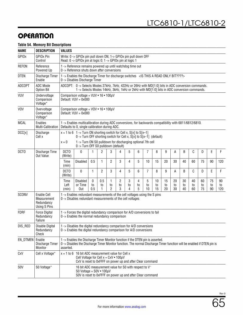
LTC6810-1/LTC6810-2
65Rev 0
For more information www.analog.com
OPERATIONTable 54. Memory Bit DescriptionsNAME DESCRIPTION VALUES
GPIOx GPIOx Pin Control
Write: 0 -> GPIOx pin pull down ON; 1-> GPIOx pin pull down OFF Read: 0 -> GPIOx pin at logic 0; 1 -> GPIOx pin at logic 1
REFON Reference Powered Up
1 -> Reference remains powered up until watchdog time out 0 -> Reference shuts down after conversions
DTEN Discharge Timer Enable
1 -> Enables the Discharge Timer for discharge switches <IS THIS A READ ONLY BIT????> 0 -> Disables Discharge Timer
ADCOPT ADC Mode Option Bit
ADCOPT: 0 -> Selects Modes 27kHz, 7kHz, 422Hz or 26Hz with MD[1:0] bits in ADC conversion commands. 1 -> Selects Modes 14kHz, 3kHz, 1kHz or 2kHz with MD[1:0] bits in ADC conversion commands.
VUV Undervoltage Comparison Voltage*
Comparison voltage = VUV • 16 • 100µV Default: VUV = 0x000
VOV Overvoltage Comparison Voltage*
Comparison voltage = VOV • 16 • 100µV Default: VUV = 0x000
MCAL Enables Multi-Calibration
1 -> Enables multicalibration during ADC conversions, for backwards compatibility with 6811/6812/6810. Defaults to 0, single calibration during ADC.
DCC[x] Discharge Cell x
x = 1 to 6 1 -> Turn ON shorting switch for Cell x, S[x] to S[x–1] 0 -> Turn OFF shorting switch for Cell x, S[x] to S[x–1] (default)
x = 0 1 -> Turn ON S0 pulldown for discharging optional 7th cell 0 -> Turn OFF S0 pulldown (default)
DCTO Discharge Time Out Value
DCTO (Write)
0 1 2 3 4 5 6 7 8 9 A B C D E F
Time (min)
Disabled 0.5 1 2 3 4 5 10 15 20 30 40 60 75 90 120
DCTO (Write)
0 1 2 3 4 5 6 7 8 9 A B C D E F
Time Left
(min)
Disabled or Time
Out
0 to 0.5
0.5 to 1
1 to 2
2 to 3
3 to 4
4 to 5
5 to 10
10 to 15
15 to 20
20 to 30
30 to 40
40 to 60
60 to 75
75 to 90
90 to
120
SCONV Enable Cell Measurement Redundancy Using S Pins
1 -> Enables redundant measurements of the cell voltages using the S pins 0 -> Disables redundant measurements of the cell voltages
FDRF Force Digital Redundancy Failure
1 -> Forces the digital redundancy comparison for A/D conversions to fail 0 -> Enables the normal redundancy comparison
DIS_RED Disable Digital Redundancy Check
1 -> Disables the digital redundancy comparison for A/D conversions 0 -> Enables the digital redundancy comparison for A/D conversions
EN_DTMEN Enable Discharge Timer Monitor
1 -> Enables the Discharge Timer Monitor function if the DTEN pin is asserted. 0 -> Disables the Discharge Timer Monitor function. The normal Discharge Timer function will be enabled if DTEN pin is asserted.
CxV Cell x Voltage* x = 1 to 6 16 bit ADC measurement value for Cell x Cell Voltage for Cell x = CxV • 100µV CxV is reset to 0xFFFF on power up and after Clear command
S0V S0 Voltage* 16 bit ADC measurement value for S0 with respect to V– S0 Voltage = S0V • 100µV S0V is reset to 0xFFFF on power up and after Clear command
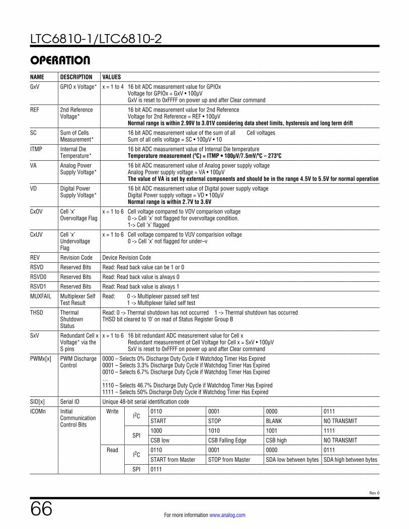
LTC6810-1/LTC6810-2
66Rev 0
For more information www.analog.com
OPERATIONNAME DESCRIPTION VALUES
GxV GPIO x Voltage* x = 1 to 4 16 bit ADC measurement value for GPIOx Voltage for GPIOx = GxV • 100µV GxV is reset to 0xFFFF on power up and after Clear command
REF 2nd Reference Voltage*
16 bit ADC measurement value for 2nd Reference Voltage for 2nd Reference = REF • 100µV Normal range is within 2.99V to 3.01V considering data sheet limits, hysteresis and long term drift
SC Sum of Cells Measurement*
16 bit ADC measurement value of the sum of all Cell voltages Sum of all cells voltage = SC • 100µV • 10
ITMP Internal Die Temperature*
16 bit ADC measurement value of Internal Die temperature Temperature measurement (ºC) = ITMP • 100µV/7.5mV/ºC – 273ºC
VA Analog Power Supply Voltage*
16 bit ADC measurement value of Analog power supply voltage Analog Power supply voltage = VA • 100µV The value of VA is set by external components and should be in the range 4.5V to 5.5V for normal operation
VD Digital Power Supply Voltage*
16 bit ADC measurement value of Digital power supply voltage Digital Power supply voltage = VD • 100µV Normal range is within 2.7V to 3.6V
CxOV Cell ‘x’ Overvoltage Flag
x = 1 to 6 Cell voltage compared to VOV comparison voltage 0 -> Cell ‘x’ not flagged for overvoltage condition. 1-> Cell ‘x’ flagged
CxUV Cell ‘x’ Undervoltage Flag
x = 1 to 6 Cell voltage compared to VUV comparision voltage 0 -> Cell ‘x’ not flagged for under–v
REV Revision Code Device Revision Code
RSVD Reserved Bits Read: Read back value can be 1 or 0
RSVD0 Reserved Bits Read: Read back value is always 0
RSVD1 Reserved Bits Read: Read back value is always 1
MUXFAIL Multiplexer Self Test Result
Read: 0 -> Multiplexer passed self test 1 -> Multiplexer failed self test
THSD Thermal Shutdown Status
Read: 0 -> Thermal shutdown has not occurred 1 -> Thermal shutdown has occurred THSD bit cleared to ‘0’ on read of Status Register Group B
SxV Redundant Cell x Voltage* via the S pins
x = 1 to 6 16 bit redundant ADC measurement value for Cell x Redundant measurement of Cell Voltage for Cell x = SxV • 100µV SxV is reset to 0xFFFF on power up and after Clear command
PWMx[x] PWM Discharge Control
0000 – Selects 0% Discharge Duty Cycle if Watchdog Timer Has Expired 0001 – Selects 3.3% Discharge Duty Cycle if Watchdog Timer Has Expired 0010 – Selects 6.7% Discharge Duty Cycle if Watchdog Timer Has Expired … 1110 – Selects 46.7% Discharge Duty Cycle if Watchdog Timer Has Expired 1111 – Selects 50% Discharge Duty Cycle if Watchdog Timer Has Expired
SID[x] Serial ID Unique 48-bit serial identification code
ICOMn Initial Communication Control Bits
WriteI2C
0110 0001 0000 0111
START STOP BLANK NO TRANSMIT
SPI1000 1010 1001 1111
CSB low CSB Falling Edge CSB high NO TRANSMIT
ReadI2C
0110 0001 0000 0111
START from Master STOP from Master SDA low between bytes SDA high between bytes
SPI 0111
LTC6810-1/LTC6810-2
67Rev 0
For more information www.analog.com
OPERATIONNAME DESCRIPTION VALUES
Dn I2C/SPI Communication Data Byte
Data transmitted(received) to(from) I2C/SPI slave device
FCOMn Final Communication Control Bits
Write I2C 0000 1000 1001
Master ACK Master NACK Master NACK + STOP
SPI X000 1001
CSB low CSB high
Read I2C 0001 0111 1111 0001 1001
ACK from Master ACK from Slave NACK from Slave ACK from Slave + STOP from Master
NACK from Slave + STOP from Master
SPI 1111
*Voltage equations use the decimal value of registers, 0 to 4095 for 12 bits and 0 to 65535 for 16 bits.
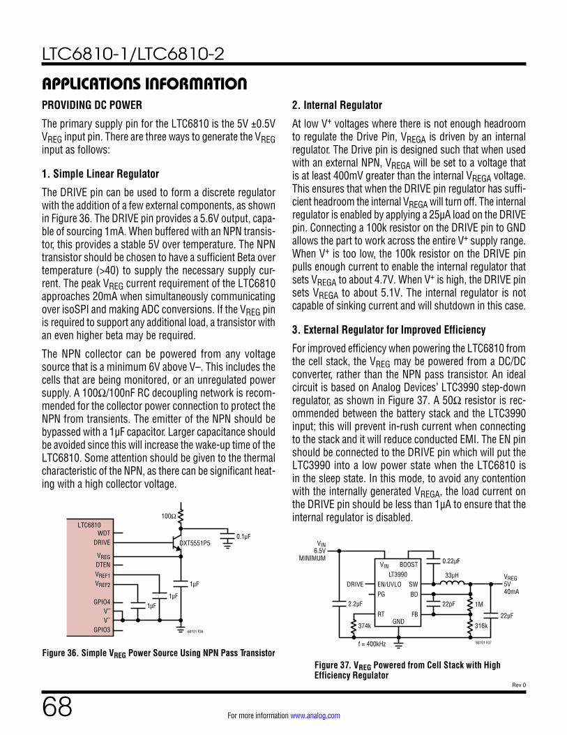
LTC6810-1/LTC6810-2
68Rev 0
For more information www.analog.com
APPLICATIONS INFORMATIONPROVIDING DC POWER
The primary supply pin for the LTC6810 is the 5V ±0.5V VREG input pin. There are three ways to generate the VREG input as follows:
1. Simple Linear Regulator
The DRIVE pin can be used to form a discrete regulator with the addition of a few external components, as shown in Figure 36. The DRIVE pin provides a 5.6V output, capa-ble of sourcing 1mA. When buffered with an NPN transis-tor, this provides a stable 5V over temperature. The NPN transistor should be chosen to have a sufficient Beta over temperature (>40) to supply the necessary supply cur-rent. The peak VREG current requirement of the LTC6810 approaches 20mA when simultaneously communicating over isoSPI and making ADC conversions. If the VREG pin is required to support any additional load, a transistor with an even higher beta may be required.
The NPN collector can be powered from any voltage source that is a minimum 6V above V–. This includes the cells that are being monitored, or an unregulated power supply. A 100Ω/100nF RC decoupling network is recom-mended for the collector power connection to protect the NPN from transients. The emitter of the NPN should be bypassed with a 1µF capacitor. Larger capacitance should be avoided since this will increase the wake-up time of the LTC6810. Some attention should be given to the thermal characteristic of the NPN, as there can be significant heat-ing with a high collector voltage.
2. Internal Regulator
At low V+ voltages where there is not enough headroom to regulate the Drive Pin, VREGA is driven by an internal regulator. The Drive pin is designed such that when used with an external NPN, VREGA will be set to a voltage that is at least 400mV greater than the internal VREGA voltage. This ensures that when the DRIVE pin regulator has suffi-cient headroom the internal VREGA will turn off. The internal regulator is enabled by applying a 25µA load on the DRIVE pin. Connecting a 100k resistor on the DRIVE pin to GND allows the part to work across the entire V+ supply range. When V+ is too low, the 100k resistor on the DRIVE pin pulls enough current to enable the internal regulator that sets VREGA to about 4.7V. When V+ is high, the DRIVE pin sets VREGA to about 5.1V. The internal regulator is not capable of sinking current and will shutdown in this case.
3. External Regulator for Improved Efficiency
For improved efficiency when powering the LTC6810 from the cell stack, the VREG may be powered from a DC/DC converter, rather than the NPN pass transistor. An ideal circuit is based on Analog Devices’ LTC3990 step-down regulator, as shown in Figure 37. A 50Ω resistor is rec-ommended between the battery stack and the LTC3990 input; this will prevent in-rush current when connecting to the stack and it will reduce conducted EMI. The EN pin should be connected to the DRIVE pin which will put the LTC3990 into a low power state when the LTC6810 is in the sleep state. In this mode, to avoid any contention with the internally generated VREGA, the load current on the DRIVE pin should be less than 1µA to ensure that the internal regulator is disabled.
Figure 37.
VIN BOOSTLT3990
SWEN/UVLOPG
RT
0.22µF
22pF
374k
f = 400kHz
22µF
2.2µF
VIN6.5V
MINIMUM
VREG5V40mA
1M
316k
33µH
BD
FBGND
DRIVE
68101 F37
VREG Powered from Cell Stack with High Efficiency Regulator
Figure 36.
1µF
0.1µF
100Ω
68101 F36
WDTDRIVE
VREGDTENVREF1VREF2
GPIO4V–
V–
GPIO3
1µF
1µF
LTC6810
DXT5551P5
Simple VREG Power Source Using NPN Pass Transistor
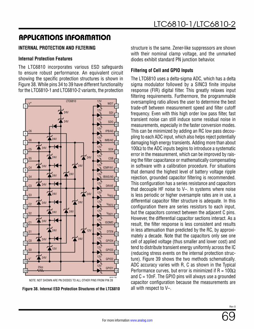
LTC6810-1/LTC6810-2
69Rev 0
For more information www.analog.com
APPLICATIONS INFORMATIONINTERNAL PROTECTION AND FILTERING
Internal Protection Features
The LTC6810 incorporates various ESD safeguards to ensure robust performance. An equivalent circuit showing the specific protection structures is shown in Figure 38. While pins 34 to 39 have different functionality for the LTC6810-1 and LTC6810-2 variants, the protection
structure is the same. Zener-like suppressors are shown with their nominal clamp voltage, and the unmarked diodes exhibit standard PN junction behavior.
Filtering of Cell and GPIO Inputs
The LTC6810 uses a delta-sigma ADC, which has a delta sigma modulator followed by a SINC3 finite impulse response (FIR) digital filter. This greatly relaxes input filtering requirements. Furthermore, the programmable oversampling ratio allows the user to determine the best trade-off between measurement speed and filter cutoff frequency. Even with this high order low pass filter, fast transient noise can still induce some residual noise in measurements, especially in the faster conversion modes. This can be minimized by adding an RC low pass decou-pling to each ADC input, which also helps reject potentially damaging high energy transients. Adding more than about 100Ω to the ADC inputs begins to introduce a systematic error in the measurement, which can be improved by rais-ing the filter capacitance or mathematically compensating in software with a calibration procedure. For situations that demand the highest level of battery voltage ripple rejection, grounded capacitor filtering is recommended. This configuration has a series resistance and capacitors that decouple HF noise to V–. In systems where noise is less periodic or higher oversample rates are in use, a differential capacitor filter structure is adequate. In this configuration there are series resistors to each input, but the capacitors connect between the adjacent C pins. However, the differential capacitor sections interact. As a result, the filter response is less consistent and results in less attenuation than predicted by the RC, by approxi-mately a decade. Note that the capacitors only see one cell of applied voltage (thus smaller and lower cost) and tend to distribute transient energy uniformly across the IC (reducing stress events on the internal protection struc-ture). Figure 39 shows the two methods schematically. ADC accuracy varies with R, C as shown in the Typical Performance curves, but error is minimized if R = 100Ω and C = 10nF. The GPIO pins will always use a grounded capacitor configuration because the measurements are all with respect to V–.Figure 38.
68101 F39
LTC6810 12V
12V
12V
12V
12V
12V
12V
12V
12V
12V
12V
12V
12V
12V
12V
12V
12V
12V
12V
NOTE: NOT SHOWN ARE PN DIODES TO ALL OTHER PINS FROM PIN 28
V+
C6
S6
C5
S5
C4
S4
C3
S3
C2
S2
C1
S1
C0
S0
V–
42
41
40
39
38
37
36
35
34
33
32
31
30
27
26
25
20
19
18
WDT
SDI
SDO
IPB/A3
IMB/A2
SCK
CSB
ICMP/A1
IBIAS/A0
DRIVE
VREG
VREF2
VREF1
ISOMD
DTEN
GPIO4
GPIO3
GPIO2
GPIO1
3
4
5
6
7
8
9
10
11
12
13
14
15
16
17
28
29
24V
24V
25Ω
24V
24V
24V
24V
24V
24V
24V
24V
24V
24V
24V
24V
24V
12V
24V
24V
24V
24V
24V
12V
24V
24V
Internal ESD Protection Structures of the LTC6810

LTC6810-1/LTC6810-2
70Rev 0
For more information www.analog.com
APPLICATIONS INFORMATION
CELL BALANCING
The LTC6810 includes signals (pins S0 through S6) that can be used to balance cells with internal or external discharge. Cells can be discharged using the internal N-channel NMOS at the S pins, or the S pins can act as digital outputs to drive external transistors. Figure 40 shows an example of internal cell balancing using the LTC6810.
Choosing a Discharge Resistor
When sizing the balancing resistor it is important to know the typical battery imbalance and the allowable time for cell balancing. In most small battery applications it is rea-sonable for the balancing circuitry to be able to correct for a 5% SOC (State Of Charge) error with 5 hours of balancing. For example a 5AHr battery with a 5% SOC imbalance will have approximately 250mAHrs of imbal-ance. Using a 50mA balancing current this could be cor-rected in 5 hours. With a 100mA balancing current, the error would be corrected in 2.5Hrs. In systems with very large batteries it becomes difficult to use passive balanc-ing to correct large SOC imbalances in short periods of time. The excessive heat created during balancing gener-ally limits the balancing current. In large capacity battery
applications if short balancing times are required an active balancing solution should be considered. When choosing a balance resistor the following equations can be used to help determine a resistor value:
Balance Current%SOC_Imbalance • Battery Capacity
Number of Hours to Balance
Balance ResistorNominal Cell Voltage
Balance Current
Figure 39.
LTC6810LTC6810
GROUNDED CAPACITOR FILTER DIFFERENTIAL CAPACITOR FILTER
68101 F39
C2
S2
C1
S1
C0
S0
100Ω
RDIS10nF
100Ω
RDIS10nF
100Ω
RDIS10nF
V–
C2
S2
C1
S1
C0
S0
100Ω
RDIS10nF
100Ω
RDIS10nF
100Ω
RDIS10nF
V–
Input Filter Structure Configurations
a)
LTC6810
68101 F41a
C(N+1)
S(N+1)
C(N)
S(N)
C(N–1)
S(N–1)
RFILTER
CFILTER
CFILTER
RFILTER
RFILTER
RDISCHARGE
RDISCHARGE
RDISCHARGE
b)
LTC6810LTC6810
68101 F41b
C(N+1)
S(N+1)
C(N)
S(N)
C(N–1)
S(N–1)
RDISCHARGE
RDISCHARGE
RDISCHARGE
C(N+1)
S(N+1)
C(N)
S(N)
C(N–1)
S(N–1)
RDISCHARGE
RDISCHARGE
RDISCHARGE
Figure 40. Internal Discharge Circuits
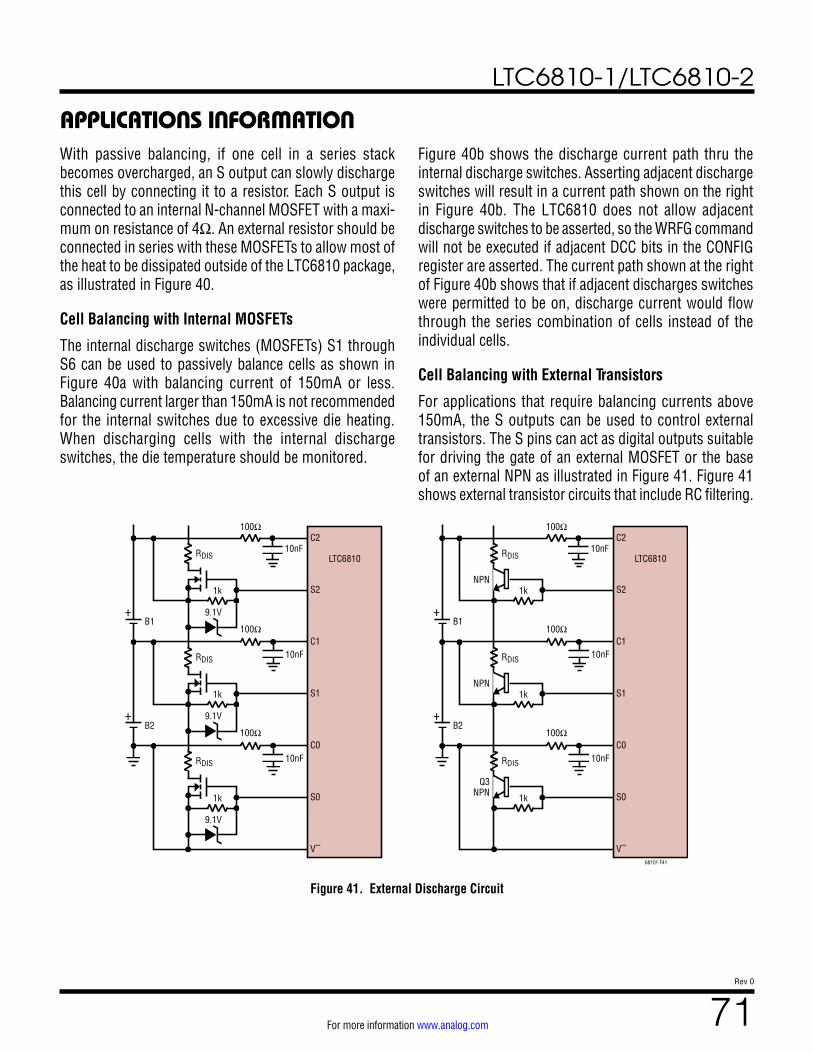
LTC6810-1/LTC6810-2
71Rev 0
For more information www.analog.com
APPLICATIONS INFORMATIONWith passive balancing, if one cell in a series stack becomes overcharged, an S output can slowly discharge this cell by connecting it to a resistor. Each S output is connected to an internal N-channel MOSFET with a maxi-mum on resistance of 4Ω. An external resistor should be connected in series with these MOSFETs to allow most of the heat to be dissipated outside of the LTC6810 package, as illustrated in Figure 40.
Cell Balancing with Internal MOSFETs
The internal discharge switches (MOSFETs) S1 through S6 can be used to passively balance cells as shown in Figure 40a with balancing current of 150mA or less. Balancing current larger than 150mA is not recommended for the internal switches due to excessive die heating. When discharging cells with the internal discharge switches, the die temperature should be monitored.
Figure 40b shows the discharge current path thru the internal discharge switches. Asserting adjacent discharge switches will result in a current path shown on the right in Figure 40b. The LTC6810 does not allow adjacent discharge switches to be asserted, so the WRFG command will not be executed if adjacent DCC bits in the CONFIG register are asserted. The current path shown at the right of Figure 40b shows that if adjacent discharges switches were permitted to be on, discharge current would flow through the series combination of cells instead of the individual cells.
Cell Balancing with External Transistors
For applications that require balancing currents above 150mA, the S outputs can be used to control external transistors. The S pins can act as digital outputs suitable for driving the gate of an external MOSFET or the base of an external NPN as illustrated in Figure 41. Figure 41 shows external transistor circuits that include RC filtering.
Figure 41.
LTC6810LTC6810
68101 F41
C2
S2
C1
S1
C0
S0
V–
100Ω
RDIS10nF
10nF
1k
100Ω
NPN
RDIS
1k
100Ω
NPN
RDIS
1k
Q3NPN
C2
S2
C1
S1
C0
S0
V–
100Ω
RDIS10nF
10nF
10nF10nF
1k
9.1V
100Ω
RDIS
1k
9.1V
100Ω
RDIS
1k
9.1V
B1
B2
B1
B2
External Discharge Circuit
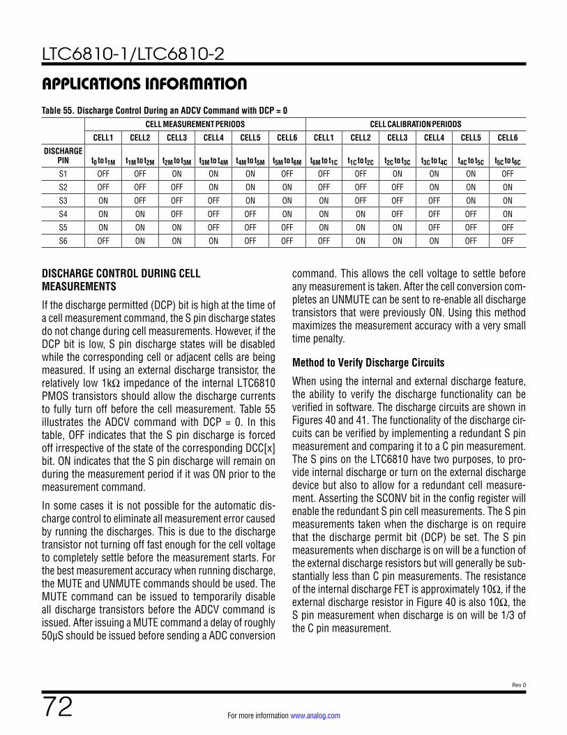
LTC6810-1/LTC6810-2
72Rev 0
For more information www.analog.com
APPLICATIONS INFORMATION
DISCHARGE CONTROL DURING CELL MEASUREMENTS
If the discharge permitted (DCP) bit is high at the time of a cell measurement command, the S pin discharge states do not change during cell measurements. However, if the DCP bit is low, S pin discharge states will be disabled while the corresponding cell or adjacent cells are being measured. If using an external discharge transistor, the relatively low 1kΩ impedance of the internal LTC6810 PMOS transistors should allow the discharge currents to fully turn off before the cell measurement. Table 55 illustrates the ADCV command with DCP = 0. In this table, OFF indicates that the S pin discharge is forced off irrespective of the state of the corresponding DCC[x] bit. ON indicates that the S pin discharge will remain on during the measurement period if it was ON prior to the measurement command.
In some cases it is not possible for the automatic dis-charge control to eliminate all measurement error caused by running the discharges. This is due to the discharge transistor not turning off fast enough for the cell voltage to completely settle before the measurement starts. For the best measurement accuracy when running discharge, the MUTE and UNMUTE commands should be used. The MUTE command can be issued to temporarily disable all discharge transistors before the ADCV command is issued. After issuing a MUTE command a delay of roughly 50µS should be issued before sending a ADC conversion
command. This allows the cell voltage to settle before any measurement is taken. After the cell conversion com-pletes an UNMUTE can be sent to re-enable all discharge transistors that were previously ON. Using this method maximizes the measurement accuracy with a very small time penalty.
Method to Verify Discharge Circuits
When using the internal and external discharge feature, the ability to verify the discharge functionality can be verified in software. The discharge circuits are shown in Figures 40 and 41. The functionality of the discharge cir-cuits can be verified by implementing a redundant S pin measurement and comparing it to a C pin measurement. The S pins on the LTC6810 have two purposes, to pro-vide internal discharge or turn on the external discharge device but also to allow for a redundant cell measure-ment. Asserting the SCONV bit in the config register will enable the redundant S pin cell measurements. The S pin measurements taken when the discharge is on require that the discharge permit bit (DCP) be set. The S pin measurements when discharge is on will be a function of the external discharge resistors but will generally be sub-stantially less than C pin measurements. The resistance of the internal discharge FET is approximately 10Ω, if the external discharge resistor in Figure 40 is also 10Ω, the S pin measurement when discharge is on will be 1/3 of the C pin measurement.
Table 55. Discharge Control During an ADCV Command with DCP = 0CELL MEASUREMENT PERIODS CELL CALIBRATION PERIODS
CELL1 CELL2 CELL3 CELL4 CELL5 CELL6 CELL1 CELL2 CELL3 CELL4 CELL5 CELL6
DISCHARGE PIN t0 to t1M t1M to t2M t2M to t3M t3M to t4M t4M to t5M t5M to t6M t6M to t1C t1C to t2C t2C to t3C t3C to t4C t4C to t5C t5C to t6C
S1 OFF OFF ON ON ON OFF OFF OFF ON ON ON OFF
S2 OFF OFF OFF ON ON ON OFF OFF OFF ON ON ON
S3 ON OFF OFF OFF ON ON ON OFF OFF OFF ON ON
S4 ON ON OFF OFF OFF ON ON ON OFF OFF OFF ON
S5 ON ON ON OFF OFF OFF ON ON ON OFF OFF OFF
S6 OFF ON ON ON OFF OFF OFF ON ON ON OFF OFF
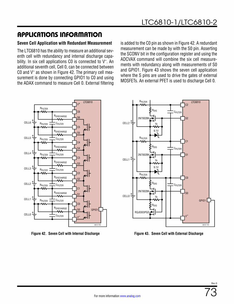
LTC6810-1/LTC6810-2
73Rev 0
For more information www.analog.com
APPLICATIONS INFORMATIONSeven Cell Application with Redundant Measurement
The LTC6810 has the ability to measure an additional sev-enth cell with redundancy and internal discharge capa-bility. In six cell applications C0 is connected to V–. An additional seventh cell, Cell 0, can be connected between C0 and V– as shown in Figure 42. The primary cell mea-surement is done by connecting GPIO1 to C0 and using the ADAX command to measure Cell 0. External filtering
is added to the C0 pin as shown in Figure 42. A redundant measurement can be made by with the S0 pin. Asserting the SCONV bit in the configuration register and using the ADCVAX command will combine the six cell measure-ments with redundancy along with measurements of S0 and GPIO1. Figure 43 shows the seven cell application where the S pins are used to drive the gates of external MOSFETs. An external PFET is used to discharge Cell 0.
Figure 42.
LTC6810
68101 F43
C6
S6
C5
S5
C4
S4
C3
S3
C2
S2
C1
S1
C0
S0
V–
RFILTER
CFILTER
CFILTER
RFILTER
RFILTER
CFILTER
RDISCHARGE
RDISCHARGE
RDISCHARGE
V+
RFILTER
CFILTER
CFILTER
RFILTER
RFILTER
CFILTER
RDISCHARGE
RDISCHARGE
RDISCHARGE
RFILTER
CFILTER
RDISCHARGE GPIO1
CELL0
CELL1
CELL2
CELL3
CELL4
CELL5
CELL6
Seven Cell with Internal Discharge Figure 43.
LTC6810
68101 F44
C2
S2
C1
S1
C0
S0
V–
RFILTER
CFILTER
2N7002BK
1k
9.1V
RDIS
GPIO1
CELL2
RFILTER
CFILTER
2N7002BK
1k
9.1V
RDIS
CELL1
RFILTER
CFILTER
2N7002BK
RQJ0303PGD
1k
RDIS
RDIS
CELL0
Seven Cell with External Discharge
LTC6810-1/LTC6810-2
74Rev 0
For more information www.analog.com
APPLICATIONS INFORMATIONDIGITAL COMMUNICATIONS
PEC Calculation
The Packet Error Code (PEC) can be used to ensure that the serial data read from the LTC6810 is valid and has not been corrupted. This is a critical feature for reliable com-munication, particularly in environments of high noise. The LTC6810 requires that a PEC be calculated for all data being read from and written to the LTC6810. For this reason it is important to have an efficient method for calculating the PEC.
The C code below provides a simple implementation of a lookup table derived PEC calculation method. There are two functions. The first function init_PEC15_Table() should only be called once when the microcontroller starts and will initialize a PEC15 table array called pec15Table[]. This table will be used in all future PEC calculations. The PEC15 table can also be hard coded into the microcon-troller rather than running the init_PEC15_Table() func-tion at startup. The pec15() function calculates the PEC and will return the correct 15 bit PEC for byte arrays of any given length.
/************************************Copyright 2012 Analog Devices, Inc.Permission to freely use, copy, modify, and distribute this software for anypurpose with or without fee is hereby granted, provided that the abovecopyright notice and this permission notice appear in all copies:THIS SOFTWARE IS PROVIDED “AS IS” AND LTC DISCLAIMS ALL WARRANTIESINCLUDING ALL IMPLIED WARRANTIES OF MERCHANTABILITY AND FITNESS. IN NOEVENT SHALL LTC BE LIABLE FOR ANY SPECIAL, DIRECT, INDIRECT, OR CONSEQUENTIALDAMAGES OR ANY DAMAGES WHATSOEVER RESULTING FROM ANY USE OF SAME, INCLUDINGANY LOSS OF USE OR DATA OR PROFITS, WHETHER IN AN ACTION OF CONTRACT, NEGLIGENCEOR OTHER TORTUOUS ACTION, ARISING OUT OF OR IN CONNECTION WITH THE USE ORPERFORMANCE OF THIS SOFTWARE.***********************************************************/int16 pec15Table[256];int16 CRC15_POLY = 0x4599;void init_PEC15_Table()for (int i = 0; i < 256; i++)remainder = i << 7;for (int bit = 8; bit > 0; --bit)if (remainder & 0x4000)remainder = ((remainder << 1));remainder = (remainder ^ CRC15_POLY)elseremainder = ((remainder << 1));pec15Table[i] = remainder&0xFFFF;unsigned int16 pec15 (char *data , int len)int16 remainder,address;remainder = 16;//PEC seedfor (int i = 0; i < len; i++)address = ((remainder >> 7) ^ data[i]) & 0xff;//calculate PEC table addressremainder = (remainder << 8 ) ^ pec15Table[address];return (remainder*2);//The CRC15 has a 0 in the LSB so the final value must be multiplied by 2

LTC6810-1/LTC6810-2
75Rev 0
For more information www.analog.com
isoSPI IBIAS and ICMP Setup
The LTC6810 allows the isoSPI links of each application to be optimized for power consumption or for noise immu-nity. The power and noise immunity of an isoSPI system is determined by the programmed IB current, which controls the isoSPI signaling currents. Bias current IB can range from 100μA to 1mA. Internal circuitry scales up this bias current to create the isoSPI signal currents equal to be 20 • IB. A low IB reduces the isoSPI power consump-tion in the READY and ACTIVE states, while a high IBincreases the amplitude of the differential signal voltage VA across the matching termination resistor, RM. The IBcurrent is programmed by the sum of the RB1 and RB2resistors connected between the 2V IBIAS pin and GND as shown in Figure 44. The receiver input threshold is set by the ICMP voltage that is programmed with the resistor divider created by the RB1 and RB2 resistors. The receiver differential threshold will be half of the voltage present on the ICMP pin.
The following guidelines should be used when setting the bias current (100µA to 1mA) IB and the receiver compara-tor threshold voltage VICMP/2:
RM = Transmission Line Characteristic Impedance Z0
Signal Amplitude VA = (20 • IB) • (RM/2)
VTCMP (Receiver Comparator Threshold) = K • VA
VICMP (Voltage on ICMP pin) = 2 • VTCMP
RB2 = VICMP/IB = 20 • K • RM
RB1 = (2/IB) – RB2
APPLICATIONS INFORMATIONSelect IB and K (Signal Amplitude VA to Receiver input threshold ratio) according to the application:
For lower power links: IB = 0.5mA and K = 0.5
For full power links: IB = 1mA and K = 0.5
For long links (>50m): IB = 1mA and K = 0.25
For addressable multidrop: IB = 1mA and K = 0.4
For applications with little system noise, setting IB to 0.5mA is a good compromise between power consump-tion and noise immunity. Using this IB setting with a 1:1 transformer and RM = 100Ω, RB1 should be set to 3.01k and RB2 set to 1k. With typical CAT5 twisted pair, these settings will allow for communication up to 50m. Applications in very noisy environments or with cables longer than 50m should increase the IB to 1mA. Higher drive current compensates for the increased insertion loss in the cable and provides high noise immunity. When using cables over 50m and a transformer with a 1:1 turns ratio and RM = 100Ω, RB1 would be 1.5k and RB2 would be 499Ω.
The length of the cable determines the maximum clock rate of an isoSPI link. For cables 10 meters or less, the maximum 1MHz SPI clock frequency is possible. As the length of the cable increases, the maximum possible SPI clock rate decreases. This dependence is a result of the increased propagation delays that can create possible tim-ing violations. Figure 45 shows how the maximum data rate reduces as the cable length increases when using a CAT 5 twisted pair.
Figure 44.
RM
IPA ISOMD VREG
IMA
+
–
+
–
IBIAS
ICMP
68101 F45
LTC6810RM
RB1
RB2
RB1
RB2
IPBISOMD
IMB
IBIAS
ICMP
MOSIMISOSCKCS
SDOSDISCKCS
LTC6810
TWISTED-PAIR CABLEWITH CHARACTERISTIC IMPEDANCE RM
ISOLATION BARRIER(MAY USE ONE OR TWO TRANFORMERS)
MASTER•• ••
2V
VA
2V
VA
isoSPI Circuit
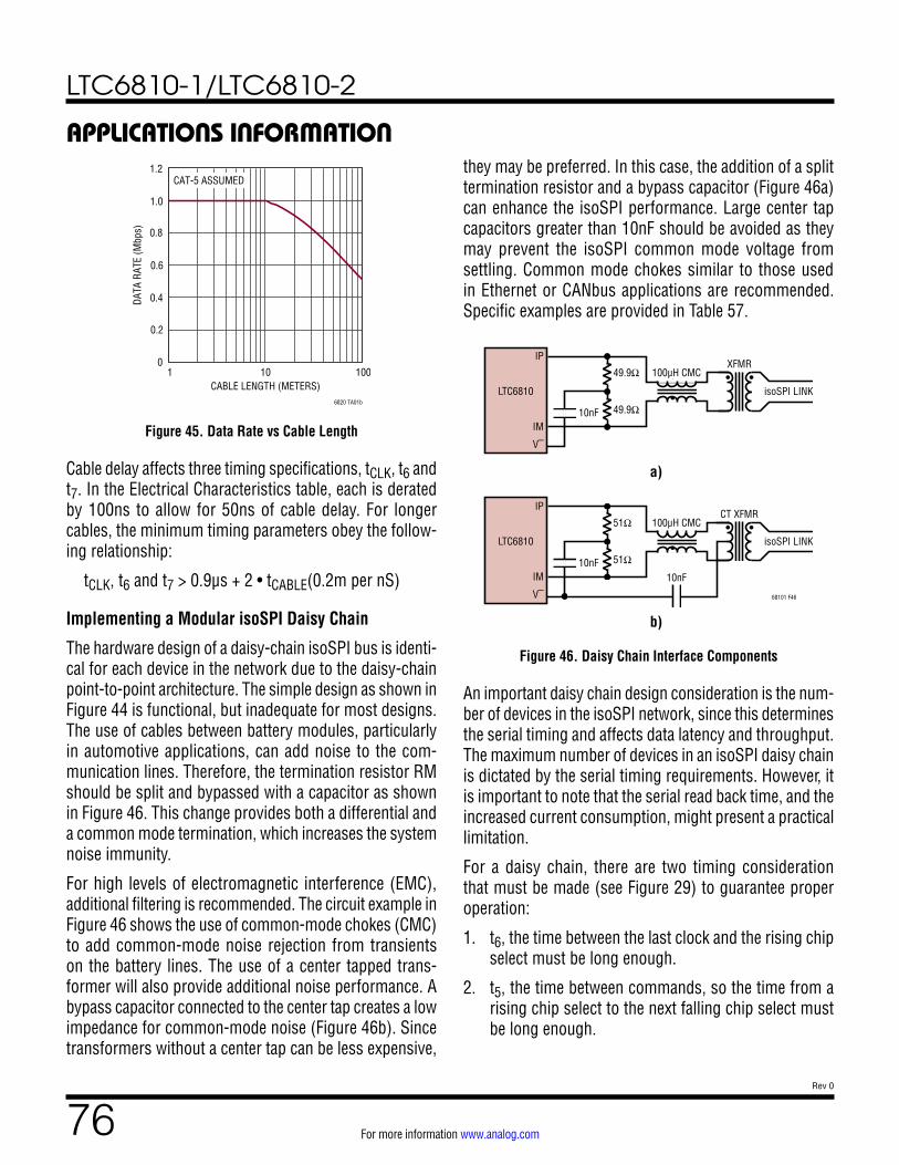
LTC6810-1/LTC6810-2
76Rev 0
For more information www.analog.com
Figure 45.
CABLE LENGTH (METERS)1
0
DATA
RAT
E (M
bps)
0.2
0.4
0.6
0.8
1.2
10 100
6820 TA01b
1.0
CAT-5 ASSUMED
Data Rate vs Cable Length
Cable delay affects three timing specifications, tCLK, t6 and t7. In the Electrical Characteristics table, each is derated by 100ns to allow for 50ns of cable delay. For longer cables, the minimum timing parameters obey the follow-ing relationship:
tCLK, t6 and t7 > 0.9μs + 2 • tCABLE(0.2m per nS)
Implementing a Modular isoSPI Daisy Chain
The hardware design of a daisy-chain isoSPI bus is identi-cal for each device in the network due to the daisy-chain point-to-point architecture. The simple design as shown in Figure 44 is functional, but inadequate for most designs. The use of cables between battery modules, particularly in automotive applications, can add noise to the com-munication lines. Therefore, the termination resistor RM should be split and bypassed with a capacitor as shown in Figure 46. This change provides both a differential and a common mode termination, which increases the system noise immunity.
For high levels of electromagnetic interference (EMC), additional filtering is recommended. The circuit example in Figure 46 shows the use of common-mode chokes (CMC)to add common-mode noise rejection from transients on the battery lines. The use of a center tapped trans-former will also provide additional noise performance. A bypass capacitor connected to the center tap creates a low impedance for common-mode noise (Figure 46b). Since transformers without a center tap can be less expensive,
APPLICATIONS INFORMATIONthey may be preferred. In this case, the addition of a split termination resistor and a bypass capacitor (Figure 46a) can enhance the isoSPI performance. Large center tap capacitors greater than 10nF should be avoided as they may prevent the isoSPI common mode voltage from settling. Common mode chokes similar to those used in Ethernet or CANbus applications are recommended. Specific examples are provided in Table 57.
Figure 46.
isoSPI LINK
XFMR
isoSPI LINK
CT XFMR
LTC6810
LTC6810
IP
IM
V–
10nF
100µH CMC
•
•49.9Ω
49.9Ω
••
a)
IP
IM
V–
10nF
100µH CMC
10nF
•
•51Ω
51Ω
••
b)
68101 F46
Daisy Chain Interface Components
An important daisy chain design consideration is the num-ber of devices in the isoSPI network, since this determines the serial timing and affects data latency and throughput. The maximum number of devices in an isoSPI daisy chain is dictated by the serial timing requirements. However, it is important to note that the serial read back time, and the increased current consumption, might present a practical limitation.
For a daisy chain, there are two timing consideration that must be made (see Figure 29) to guarantee proper operation:
1. t6, the time between the last clock and the rising chip select must be long enough.
2. t5, the time between commands, so the time from a rising chip select to the next falling chip select must be long enough.
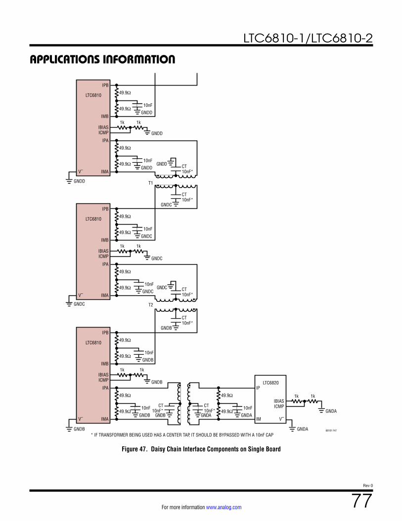
LTC6810-1/LTC6810-2
77Rev 0
For more information www.analog.com
APPLICATIONS INFORMATION
Figure 47.
10nF
GNDD
10nF
GNDD
GNDD
GNDD
10nF
GNDC
10nF
GNDC
GNDC
GNDC
10nF
GNDB
10nF
GNDB
GNDB
10nF
GNDA
GNDB
GNDACT10nF*
CT10nF*
1k 1k
••
GNDC
1k 1k
•
•
GNDB
1k 1k
1k 1k
••
GNDA
GNDD
GNDB GNDA
CT10nF*
GNDC CT10nF*
CT10nF*
CT10nF*
49.9Ω
49.9Ω
IPA
IBIASICMP
LTC6810
IMA
49.9Ω
49.9Ω
IPB
IMB
49.9Ω
49.9Ω
IPA
IBIASICMP
LTC6810
IMA
49.9Ω
49.9Ω
IPB
IMB
49.9Ω
49.9Ω
IPA
IBIASICMP
IBIASICMP
LTC6810
V–
V–
V–
IMA
49.9Ω
49.9Ω
IP
IM V–
49.9Ω
49.9Ω
IPB
IMB
* IF TRANSFORMER BEING USED HAS A CENTER TAP, IT SHOULD BE BYPASSED WITH A 10nF CAP68101 F47
LTC6820
T1
T2
Daisy Chain Interface Components on Single Board
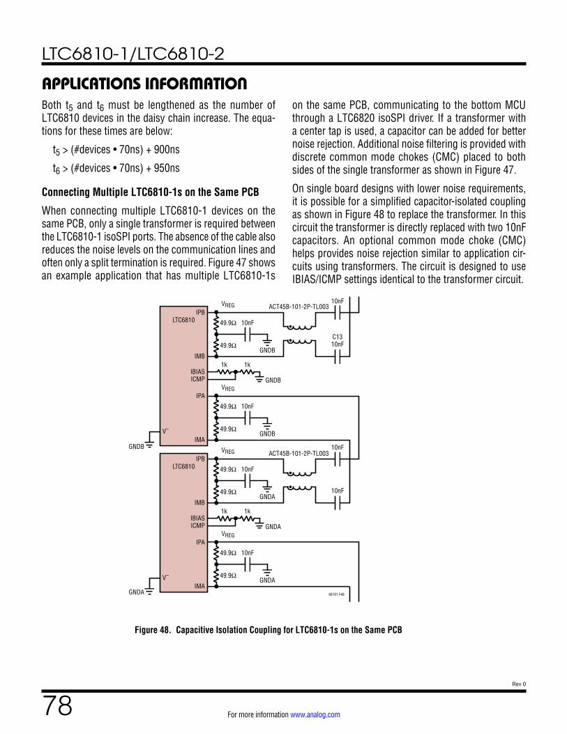
LTC6810-1/LTC6810-2
78Rev 0
For more information www.analog.com
APPLICATIONS INFORMATIONBoth t5 and t6 must be lengthened as the number of LTC6810 devices in the daisy chain increase. The equa-tions for these times are below:
t5 > (#devices • 70ns) + 900ns
t6 > (#devices • 70ns) + 950ns
Connecting Multiple LTC6810-1s on the Same PCB
When connecting multiple LTC6810-1 devices on the same PCB, only a single transformer is required between the LTC6810-1 isoSPI ports. The absence of the cable also reduces the noise levels on the communication lines and often only a split termination is required. Figure 47 shows an example application that has multiple LTC6810-1s
on the same PCB, communicating to the bottom MCU through a LTC6820 isoSPI driver. If a transformer with a center tap is used, a capacitor can be added for better noise rejection. Additional noise filtering is provided with discrete common mode chokes (CMC) placed to both sides of the single transformer as shown in Figure 47.
On single board designs with lower noise requirements, it is possible for a simplified capacitor-isolated coupling as shown in Figure 48 to replace the transformer. In this circuit the transformer is directly replaced with two 10nF capacitors. An optional common mode choke (CMC) helps provides noise rejection similar to application cir-cuits using transformers. The circuit is designed to use IBIAS/ICMP settings identical to the transformer circuit.
Figure 48.
10nF
GNDB
GNDB
GNDB
VREG
10nF
GNDB
VREG
10nF
GNDA
GNDA
GNDA
VREG
10nF
GNDA
VREG
68101 F48
10nF
C1310nF
10nF
10nF
1k 1k
1k 1k
••
••
IPA
IBIASICMP
LTC6810
IMA
49.9Ω
49.9Ω
49.9Ω
49.9Ω
IPB
IMB
V–
IPA
IBIASICMP
LTC6810
IMA
49.9Ω
49.9Ω
49.9Ω
49.9Ω
IPB
IMB
V–
ACT45B-101-2P-TL003
ACT45B-101-2P-TL003
Capacitive Isolation Coupling for LTC6810-1s on the Same PCB
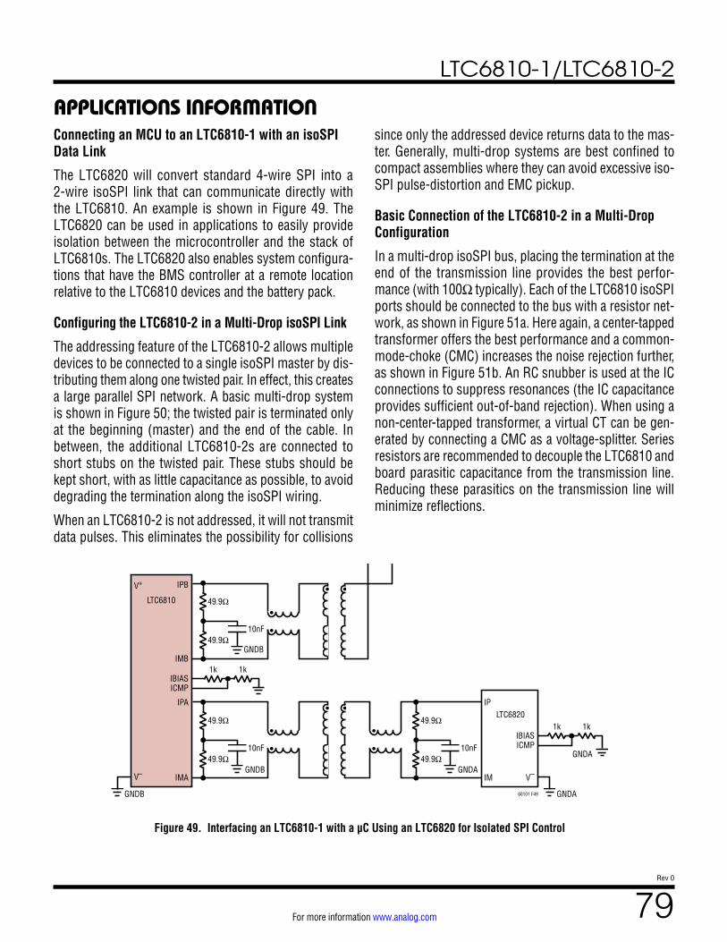
LTC6810-1/LTC6810-2
79Rev 0
For more information www.analog.com
APPLICATIONS INFORMATIONConnecting an MCU to an LTC6810-1 with an isoSPI Data Link
The LTC6820 will convert standard 4-wire SPI into a 2-wire isoSPI link that can communicate directly with the LTC6810. An example is shown in Figure 49. The LTC6820 can be used in applications to easily provide isolation between the microcontroller and the stack of LTC6810s. The LTC6820 also enables system configura-tions that have the BMS controller at a remote location relative to the LTC6810 devices and the battery pack.
Configuring the LTC6810-2 in a Multi-Drop isoSPI Link
The addressing feature of the LTC6810-2 allows multiple devices to be connected to a single isoSPI master by dis-tributing them along one twisted pair. In effect, this creates a large parallel SPI network. A basic multi-drop system is shown in Figure 50; the twisted pair is terminated only at the beginning (master) and the end of the cable. In between, the additional LTC6810-2s are connected to short stubs on the twisted pair. These stubs should be kept short, with as little capacitance as possible, to avoid degrading the termination along the isoSPI wiring.
When an LTC6810-2 is not addressed, it will not transmit data pulses. This eliminates the possibility for collisions
since only the addressed device returns data to the mas-ter. Generally, multi-drop systems are best confined to compact assemblies where they can avoid excessive iso-SPI pulse-distortion and EMC pickup.
Basic Connection of the LTC6810-2 in a Multi-Drop Configuration
In a multi-drop isoSPI bus, placing the termination at the end of the transmission line provides the best perfor-mance (with 100Ω typically). Each of the LTC6810 isoSPI ports should be connected to the bus with a resistor net-work, as shown in Figure 51a. Here again, a center-tapped transformer offers the best performance and a common-mode-choke (CMC) increases the noise rejection further, as shown in Figure 51b. An RC snubber is used at the IC connections to suppress resonances (the IC capacitance provides sufficient out-of-band rejection). When using a non-center-tapped transformer, a virtual CT can be gen-erated by connecting a CMC as a voltage-splitter. Series resistors are recommended to decouple the LTC6810 and board parasitic capacitance from the transmission line. Reducing these parasitics on the transmission line will minimize reflections.
Figure 49.
10nF
GNDB
GNDB
10nF
GNDA
GNDA
10nF
GNDB
1k 1k
1k 1k
•
GNDA
•
••
••
••
•
•
49.9Ω
49.9Ω
49.9Ω
49.9Ω
IPA
IBIASICMP
IBIASICMP
LTC6810
IMA
49.9Ω
49.9Ω
IP
IM V–
IPB
IMB
68101 F49
LTC6820
V–
V+
Interfacing an LTC6810-1 with a µC Using an LTC6820 for Isolated SPI Control
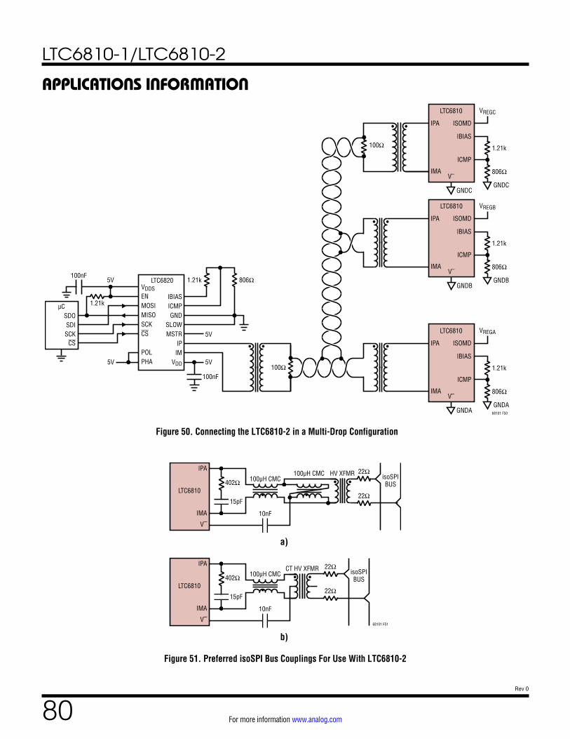
LTC6810-1/LTC6810-2
80Rev 0
For more information www.analog.com
APPLICATIONS INFORMATION
Figure 50.
1.21k
806Ω
IPA
IBIAS
ISOMD
IMAV–
VREGB
ICMP
LTC6810
1.21k
806Ω
IPA
IBIAS
ISOMD
IMAV–
VREGA
ICMP
68101 F50
LTC6810
1.21k
806Ω
GNDB
GNDA
GNDC
GNDB
GNDA
GNDC
IPA
IBIAS
ISOMD
IMAV–
VREGC
ICMP
LTC6810
••
••
••••
100Ω
1.21k 806Ω
1.21k
100nF
IBIASICMPGND
SLOWMSTR
IPIM
VDD
VDDSENMOSIMISOSCKCS
POLPHA 5V5V
5V
5V
LTC6820100nF
µCSDO
CS
SDISCK
100Ω
Connecting the LTC6810-2 in a Multi-Drop Configuration
Figure 51.
isoSPIBUS
HV XFMR
CT HV XFMR
22Ω
22Ω
22Ω
22Ω
isoSPIBUS
LTC6810
LTC6810
IPA
IMA
V–
15pF
100µH CMC
10nF
•
•100µH CMC
•
•402Ω
15pF
402Ω
••
a)
IPA
IMA
V–
100µH CMC
10nF
•
• ••
b)
68101 F51
Preferred isoSPI Bus Couplings For Use With LTC6810-2
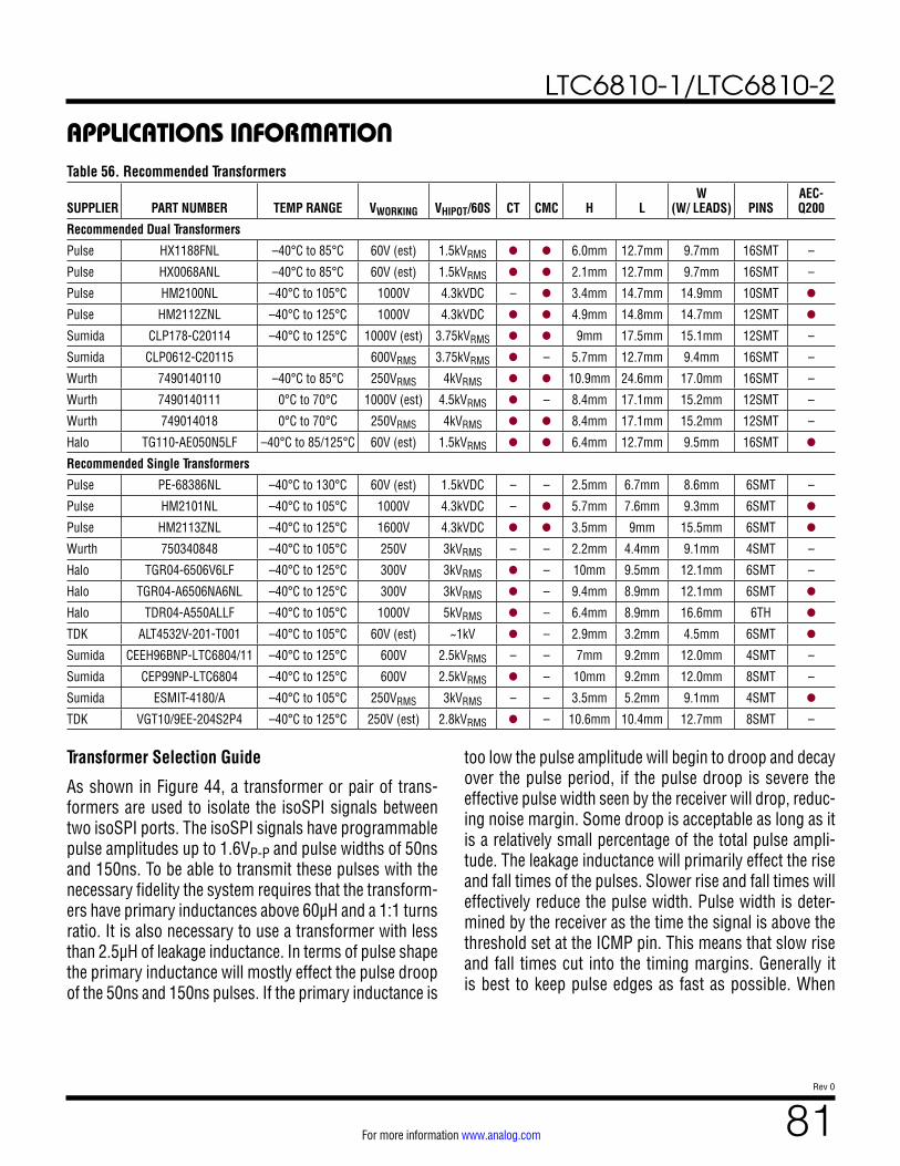
LTC6810-1/LTC6810-2
81Rev 0
For more information www.analog.com
APPLICATIONS INFORMATION
Transformer Selection Guide
As shown in Figure 44, a transformer or pair of trans-formers are used to isolate the isoSPI signals between two isoSPI ports. The isoSPI signals have programmable pulse amplitudes up to 1.6VP-P and pulse widths of 50ns and 150ns. To be able to transmit these pulses with the necessary fidelity the system requires that the transform-ers have primary inductances above 60µH and a 1:1 turns ratio. It is also necessary to use a transformer with less than 2.5µH of leakage inductance. In terms of pulse shape the primary inductance will mostly effect the pulse droop of the 50ns and 150ns pulses. If the primary inductance is
too low the pulse amplitude will begin to droop and decay over the pulse period, if the pulse droop is severe the effective pulse width seen by the receiver will drop, reduc-ing noise margin. Some droop is acceptable as long as it is a relatively small percentage of the total pulse ampli-tude. The leakage inductance will primarily effect the rise and fall times of the pulses. Slower rise and fall times will effectively reduce the pulse width. Pulse width is deter-mined by the receiver as the time the signal is above the threshold set at the ICMP pin. This means that slow rise and fall times cut into the timing margins. Generally it is best to keep pulse edges as fast as possible. When
Table 56. Recommended Transformers
SUPPLIER PART NUMBER TEMP RANGE VWORKING VHIPOT/60S CT CMC H LW
(W/ LEADS) PINSAEC- Q200
Recommended Dual Transformers
Pulse HX1188FNL –40°C to 85°C 60V (est) 1.5kVRMS l l 6.0mm 12.7mm 9.7mm 16SMT –
Pulse HX0068ANL –40°C to 85°C 60V (est) 1.5kVRMS l l 2.1mm 12.7mm 9.7mm 16SMT –
Pulse HM2100NL –40°C to 105°C 1000V 4.3kVDC – l 3.4mm 14.7mm 14.9mm 10SMT l
Pulse HM2112ZNL –40°C to 125°C 1000V 4.3kVDC l l 4.9mm 14.8mm 14.7mm 12SMT l
Sumida CLP178-C20114 –40°C to 125°C 1000V (est) 3.75kVRMS l l 9mm 17.5mm 15.1mm 12SMT –
Sumida CLP0612-C20115 600VRMS 3.75kVRMS l – 5.7mm 12.7mm 9.4mm 16SMT –
Wurth 7490140110 –40°C to 85°C 250VRMS 4kVRMS l l 10.9mm 24.6mm 17.0mm 16SMT –
Wurth 7490140111 0°C to 70°C 1000V (est) 4.5kVRMS l – 8.4mm 17.1mm 15.2mm 12SMT –
Wurth 749014018 0°C to 70°C 250VRMS 4kVRMS l l 8.4mm 17.1mm 15.2mm 12SMT –
Halo TG110-AE050N5LF –40°C to 85/125°C 60V (est) 1.5kVRMS l l 6.4mm 12.7mm 9.5mm 16SMT l
Recommended Single Transformers
Pulse PE-68386NL –40°C to 130°C 60V (est) 1.5kVDC – – 2.5mm 6.7mm 8.6mm 6SMT –
Pulse HM2101NL –40°C to 105°C 1000V 4.3kVDC – l 5.7mm 7.6mm 9.3mm 6SMT l
Pulse HM2113ZNL –40°C to 125°C 1600V 4.3kVDC l l 3.5mm 9mm 15.5mm 6SMT l
Wurth 750340848 –40°C to 105°C 250V 3kVRMS – – 2.2mm 4.4mm 9.1mm 4SMT –
Halo TGR04-6506V6LF –40°C to 125°C 300V 3kVRMS l – 10mm 9.5mm 12.1mm 6SMT –
Halo TGR04-A6506NA6NL –40°C to 125°C 300V 3kVRMS l – 9.4mm 8.9mm 12.1mm 6SMT l
Halo TDR04-A550ALLF –40°C to 105°C 1000V 5kVRMS l – 6.4mm 8.9mm 16.6mm 6TH l
TDK ALT4532V-201-T001 –40°C to 105°C 60V (est) ~1kV l – 2.9mm 3.2mm 4.5mm 6SMT l
Sumida CEEH96BNP-LTC6804/11 –40°C to 125°C 600V 2.5kVRMS – – 7mm 9.2mm 12.0mm 4SMT –
Sumida CEP99NP-LTC6804 –40°C to 125°C 600V 2.5kVRMS l – 10mm 9.2mm 12.0mm 8SMT –
Sumida ESMIT-4180/A –40°C to 105°C 250VRMS 3kVRMS – – 3.5mm 5.2mm 9.1mm 4SMT l
TDK VGT10/9EE-204S2P4 –40°C to 125°C 250V (est) 2.8kVRMS l – 10.6mm 10.4mm 12.7mm 8SMT –
LTC6810-1/LTC6810-2
82Rev 0
For more information www.analog.com
APPLICATIONS INFORMATIONevaluating transformers it is also worth noting is the par-allel winding capacitance. While transformers have very good CMRR at low frequency, this rejection will degrade at higher frequencies and this is largely due to the winding to winding capacitance. So when choosing a transformer it is best to pick one with less parallel winding capacitance when possible.
When choosing a transformer it is equally important to pick a part that has an adequate isolation rating for the application. The working voltage rating of a transformer is a key spec when selecting a part for an applications. Interconnecting daisy chain links between LTC6810-1 devices will typically see <60V stress, so ordinary pulse and LAN type transformers will suffice. Multi-drop con-nections and connections to the LTC6820 in general may need much higher working voltage ratings for good long-term reliability. Usually matching the working voltage to the voltage of the entire battery stack is conservative. Unfortunately, transformer vendors will often only spec-ify one-second HV testing, and this is not equal to the long-term (‘permanent’) rating of the part. For example, according to most safety standards a 1.5kV rated trans-former is expected to handle 230V continuously, and a 3kV device is capable of 1100V long-term, though manu-facturers may not always certify to those levels (refer to actual vendor data for specifics). Usually the higher volt-age transformers are called ‘high-isolation’ or ‘reinforced insulation’ types by the suppliers. Table 56 shows a list of transformers that have been evaluated in isoSPI links.
In most applications a common mode choke is also nec-essary for noise rejection. Table 57 includes a list of suit-able CMCs if the CMC is not already integrated into the transformer being used.
Table 57. Recommended Common Mode ChokesMANUFACTURER PART NUMBER
TDK ACT45B-101-2P
Murata DLW43SH101XK2
isoSPI Layout Guidelines
Layout of the isoSPI signal lines also plays a significant role in maximizing the noise immunity of a data link. The following layout guidelines are recommended:
1. The transformer should be placed as close to the isoSPI cable connector as possible. The distance should be kept less than 2cm. The LTC6810 should be placed close to but at least 1cm to 2cm away from the transformer to help isolate the IC from magnetic field coupling.
2. A V– ground plane should not extend under the trans-former, the isoSPI connector, or in between the trans-former and the connector.
3. The isoSPI signal traces should be as direct as pos-sible while isolated from adjacent circuitry by ground metal or space. No traces should cross the isoSPI signal lines, unless separated by a ground plane on an inner layer.
System Supply Current
The LTC6810 has various supply current specifications for the different states of operation. The average sup-ply current dependents on the control loop in the sys-tem. It is necessary to know which commands are being executed each control loop cycle, and the duration of the control loop cycle. From this information it is possible to determine the percentage of time the LTC6810 is in the measure state versus the low power sleep state. The amount of isoSPI or SPI communication will also affect the average supply current.
Calculating Serial Throughput
For any given LTC6810 the calculation to determine com-munication time is simple, it is the number of bits in the transmission multiplied by the SPI clock period being used. The control protocol of the LTC6810 is very uni-form so almost all commands can be categorized as a write, read or an operation. The tables below can be used to determine the number of bits in a given LTC6810 com-mand. Table 58 can be used for daisy-chains and Table 59 for multi-drop networks.
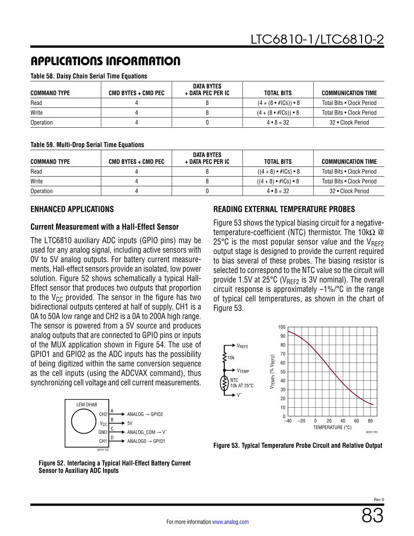
LTC6810-1/LTC6810-2
83Rev 0
For more information www.analog.com
Table 58. Daisy Chain Serial Time Equations
COMMAND TYPE CMD BYTES + CMD PECDATA BYTES
+ DATA PEC PER IC TOTAL BITS COMMUNICATION TIME
Read 4 8 (4 + (8 • #ICs)) • 8 Total Bits • Clock Period
Write 4 8 (4 + (8 • #ICs)) • 8 Total Bits • Clock Period
Operation 4 0 4 • 8 = 32 32 • Clock Period
Table 59. Multi-Drop Serial Time Equations
COMMAND TYPE CMD BYTES + CMD PECDATA BYTES
+ DATA PEC PER IC TOTAL BITS COMMUNICATION TIME
Read 4 8 ((4 + 8) • #ICs) • 8 Total Bits • Clock Period
Write 4 8 ((4 + 8) • #ICs) • 8 Total Bits • Clock Period
Operation 4 0 4 • 8 = 32 32 • Clock Period
APPLICATIONS INFORMATION
ENHANCED APPLICATIONS
Current Measurement with a Hall-Effect Sensor
The LTC6810 auxiliary ADC inputs (GPIO pins) may be used for any analog signal, including active sensors with 0V to 5V analog outputs. For battery current measure-ments, Hall-effect sensors provide an isolated, low power solution. Figure 52 shows schematically a typical Hall-Effect sensor that produces two outputs that proportion to the VCC provided. The sensor in the figure has two bidirectional outputs centered at half of supply, CH1 is a 0A to 50A low range and CH2 is a 0A to 200A high range. The sensor is powered from a 5V source and produces analog outputs that are connected to GPIO pins or inputs of the MUX application shown in Figure 54. The use of GPIO1 and GPIO2 as the ADC inputs has the possibility of being digitized within the same conversion sequence as the cell inputs (using the ADCVAX command), thus synchronizing cell voltage and cell current measurements.
Figure 52.
68101 F52
LEM DHAB
CH2 ANALOG → GPIO2
VCC 5V
GND ANALOG_COM → V–
CH1 ANALOG0 → GPIO1
A
B
C
D
Interfacing a Typical Hall-Effect Battery Current Sensor to Auxiliary ADC Inputs
READING EXTERNAL TEMPERATURE PROBES
Figure 53 shows the typical biasing circuit for a negative-temperature-coefficient (NTC) thermistor. The 10kΩ @ 25°C is the most popular sensor value and the VREF2output stage is designed to provide the current required to bias several of these probes. The biasing resistor is selected to correspond to the NTC value so the circuit will provide 1.5V at 25°C (VREF2 is 3V nominal). The overall circuit response is approximately –1%/°C in the range of typical cell temperatures, as shown in the chart of Figure 53.
Figure 53.
TEMPERATURE (°C)–40 0
V TEM
Px (%
VRE
F2)
100
80
60
40
20
90
70
50
30
10
0–20 20 6040 80
68101 F53
10k
NTC10k AT 25°C
V–
VREF2
VTEMP
Typical Temperature Probe Circuit and Relative Output
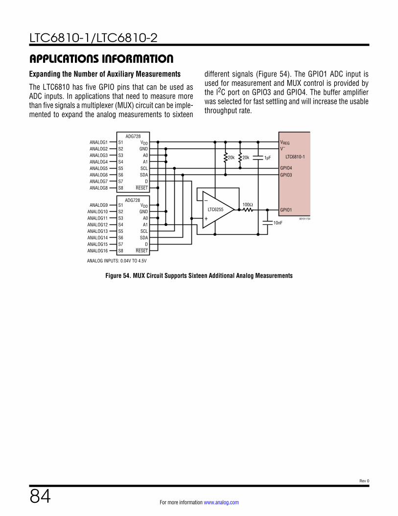
LTC6810-1/LTC6810-2
84Rev 0
For more information www.analog.com
Expanding the Number of Auxiliary Measurements
The LTC6810 has five GPIO pins that can be used as ADC inputs. In applications that need to measure more than five signals a multiplexer (MUX) circuit can be imple-mented to expand the analog measurements to sixteen
APPLICATIONS INFORMATIONdifferent signals (Figure 54). The GPIO1 ADC input is used for measurement and MUX control is provided by the I2C port on GPIO3 and GPIO4. The buffer amplifier was selected for fast settling and will increase the usable throughput rate.
Figure 54.
S1S2S3S4S5S6S7S8
VDDGND
A0A1
SCLSDA
DRESET
ANALOG1ANALOG2ANALOG3ANALOG4ANALOG5ANALOG6ANALOG7ANALOG8
ADG728
S1S2S3S4S5S6S7S8
VDDGND
A0A1
SCLSDA
DRESET
ANALOG9ANALOG10ANALOG11ANALOG12ANALOG13ANALOG14ANALOG15ANALOG16
ADG728
1µF
10nF68101 F54
VREG
GPIO4GPIO3
V–
GPIO1
LTC6810-120k20k
–
+LTC6255
100Ω
ANALOG INPUTS: 0.04V TO 4.5V
MUX Circuit Supports Sixteen Additional Analog Measurements
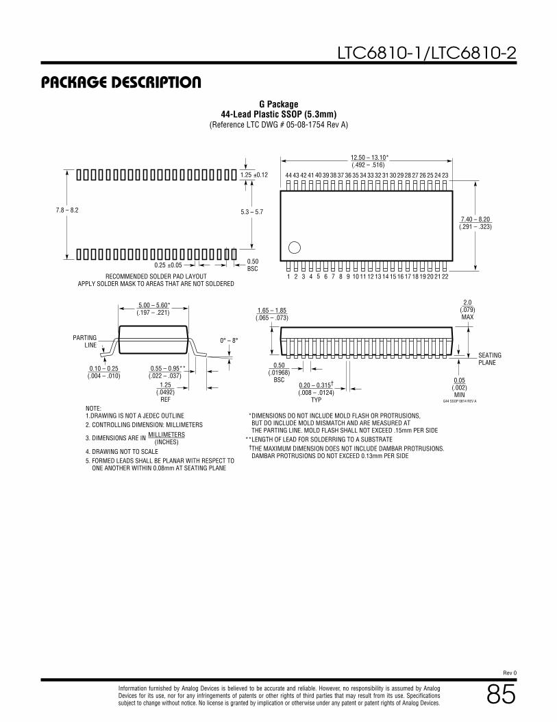
LTC6810-1/LTC6810-2
85Rev 0
For more information www.analog.com
Information furnished by Analog Devices is believed to be accurate and reliable. However, no responsibility is assumed by Analog Devices for its use, nor for any infringements of patents or other rights of third parties that may result from its use. Specifications subject to change without notice. No license is granted by implication or otherwise under any patent or patent rights of Analog Devices.
PACKAGE DESCRIPTION
G44 SSOP 0814 REV A
0.10 – 0.25(.004 – .010)
0° – 8°
SEATINGPLANE
0.55 – 0.95**(.022 – .037)
1.25(.0492)
REF
5.00 – 5.60*(.197 – .221)
7.40 – 8.20(.291 – .323)
1 2 3 4 5 6 7 8 9 10 11 12 14 15 16 17 18 19 20 21 2213
44 43 42 41 40 39 38 37 36 35 34 33 31 30 29 28 27 26 25 24 2332
12.50 – 13.10*(.492 – .516)
2.0(.079)MAX
1.65 – 1.85(.065 – .073)
0.05(.002)MIN
0.50(.01968)
BSC0.20 – 0.315†
(.008 – .0124)TYP
MILLIMETERS(INCHES)
DIMENSIONS DO NOT INCLUDE MOLD FLASH OR PROTRUSIONS,BUT DO INCLUDE MOLD MISMATCH AND ARE MEASURED ATTHE PARTING LINE. MOLD FLASH SHALL NOT EXCEED .15mm PER SIDELENGTH OF LEAD FOR SOLDERRING TO A SUBSTRATETHE MAXIMUM DIMENSION DOES NOT INCLUDE DAMBAR PROTRUSIONS.DAMBAR PROTRUSIONS DO NOT EXCEED 0.13mm PER SIDE
*
**†
NOTE:1.DRAWING IS NOT A JEDEC OUTLINE2. CONTROLLING DIMENSION: MILLIMETERS
3. DIMENSIONS ARE IN
4. DRAWING NOT TO SCALE5. FORMED LEADS SHALL BE PLANAR WITH RESPECT TO ONE ANOTHER WITHIN 0.08mm AT SEATING PLANE
0.25 ±0.05
PARTINGLINE
0.50BSC
5.3 – 5.77.8 – 8.2
RECOMMENDED SOLDER PAD LAYOUTAPPLY SOLDER MASK TO AREAS THAT ARE NOT SOLDERED
1.25 ±0.12
G Package44-Lead Plastic SSOP (5.3mm)
(Reference LTC DWG # 05-08-1754 Rev A)
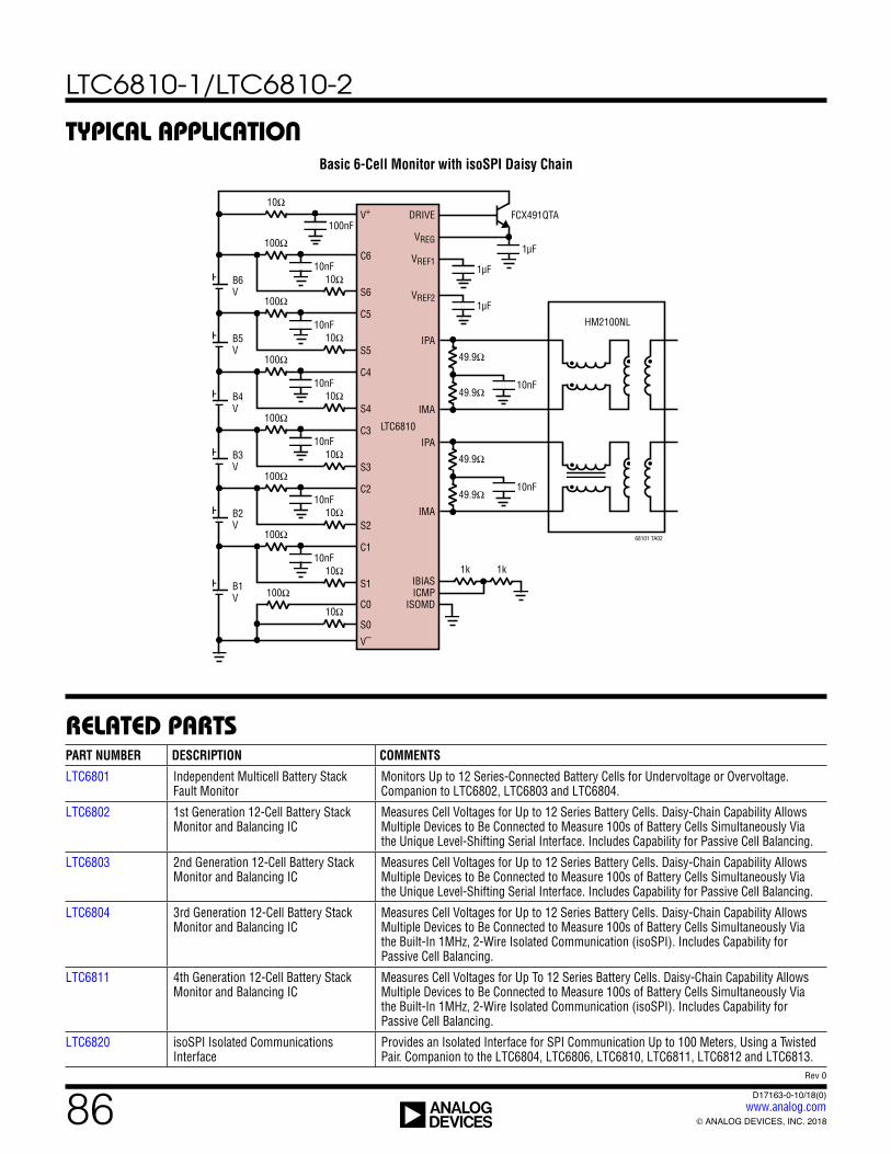
LTC6810-1/LTC6810-2
86Rev 0
For more information www.analog.com ANALOG DEVICES, INC. 2018
D17163-0-10/18(0)www.analog.com
RELATED PARTS
TYPICAL APPLICATION
PART NUMBER DESCRIPTION COMMENTS
LTC6801 Independent Multicell Battery Stack Fault Monitor
Monitors Up to 12 Series-Connected Battery Cells for Undervoltage or Overvoltage. Companion to LTC6802, LTC6803 and LTC6804.
LTC6802 1st Generation 12-Cell Battery Stack Monitor and Balancing IC
Measures Cell Voltages for Up to 12 Series Battery Cells. Daisy-Chain Capability Allows Multiple Devices to Be Connected to Measure 100s of Battery Cells Simultaneously Via the Unique Level-Shifting Serial Interface. Includes Capability for Passive Cell Balancing.
LTC6803 2nd Generation 12-Cell Battery Stack Monitor and Balancing IC
Measures Cell Voltages for Up to 12 Series Battery Cells. Daisy-Chain Capability Allows Multiple Devices to Be Connected to Measure 100s of Battery Cells Simultaneously Via the Unique Level-Shifting Serial Interface. Includes Capability for Passive Cell Balancing.
LTC6804 3rd Generation 12-Cell Battery Stack Monitor and Balancing IC
Measures Cell Voltages for Up to 12 Series Battery Cells. Daisy-Chain Capability Allows Multiple Devices to Be Connected to Measure 100s of Battery Cells Simultaneously Via the Built-In 1MHz, 2-Wire Isolated Communication (isoSPI). Includes Capability for Passive Cell Balancing.
LTC6811 4th Generation 12-Cell Battery Stack Monitor and Balancing IC
Measures Cell Voltages for Up To 12 Series Battery Cells. Daisy-Chain Capability Allows Multiple Devices to Be Connected to Measure 100s of Battery Cells Simultaneously Via the Built-In 1MHz, 2-Wire Isolated Communication (isoSPI). Includes Capability for Passive Cell Balancing.
LTC6820 isoSPI Isolated Communications Interface
Provides an Isolated Interface for SPI Communication Up to 100 Meters, Using a Twisted Pair. Companion to the LTC6804, LTC6806, LTC6810, LTC6811, LTC6812 and LTC6813.
Basic 6-Cell Monitor with isoSPI Daisy Chain
10nF
10nF
1k 1k
C1
S110Ω
100Ω
100Ω
100Ω
100Ω
100Ω
100Ω
10nF
100Ω
10Ω
V–
B1V
C2
S210Ω
10nFB2V
C3
S310Ω
10nFB3V
C4
S410Ω
10nFB4V
C5
S510Ω
10nFB5V
C6
S610Ω
10nF
DRIVE
VREG
VREF1
VREF2
1µF
1µF
10ΩV+
100nF
B6V
1µF
FCX491QTA
68101 TA02
49.9Ω
49.9Ω
IPA
IBIASICMP
ISOMD
LTC6810
IMA
HM2100NL
49.9Ω
49.9Ω
IPA
IMA
C0
S0


![DODGE CHALLENGER AUTHENTIC ACCESSORIESor 6.4L ®HEMI engines. [ 05038041A A ] F. BATTERY CHARGER. Continuously monitors your vehicle’s battery charge [ level. 82213378AB ] G. PORTED](https://img.pdfslide.us/doc/110x75/5e9b68f9267ebb7ed22c783b/dodge-challenger-authentic-or-64l-hemi-engines-05038041a-a-f-battery-charger.jpg)