Embed Size (px)
Citation preview
LTC6405
16405fb
For more information www.linear.com/6405
L, LT, LTC, LTM, Linear Technology and the Linear logo are registered trademarks of Linear Technology Corporation. All other trademarks are the property of their respective owners.
Features
applications
Description
2.7GHz, 5V, Low Noise, Rail-to-Rail Input Differential
Amplifier/Driver
The LTC®6405 is a very low noise, low distortion, fully differential input/output amplifier optimized for 5V, single supply operation. The LTC6405 input common mode range is rail-to-rail, while the output common mode voltage is independently adjustable by applying a voltage on the VOCM pin. This makes the LTC6405 ideal for level shifting signals with a wide common mode range for driving 12-bit to 16-bit single supply, differential input ADCs.
A 2.7GHz gain-bandwidth product results in 65dB linearity for 50MHz input signals. The LTC6405 is unity gain stable and the closed-loop bandwidth extends from DC to 800MHz. The output voltage swing extends from near-ground to 4V, to be compatible with a wide range of ADC converter input requirements. The LTC6405 draws only 18mA, and has a hardware shutdown feature which reduces current consumption to 400µA.
The LTC6405 is available in a compact 3mm × 3mm 16-pin leadless QFN package, as well as an 8-lead MSOP package, and operates over a –40°C to 85°C temperature range.
Single-Ended Input to Differential Output with Common Mode Level Shifting
n Low Noise: 1.6nV/√Hz RTIn Low Power: 18mA at 5Vn Low Distortion (HD2/HD3):
–82dBc/–65dBc at 50MHz, 2VP-P –97dBc/–91dBc at 25MHz, 2VP-P
n Rail-to-Rail Differential Inputn 4.5V to 5.25V Supply Voltage Rangen Fully Differential Input and Outputn Adjustable Output Common Mode Voltagen 800MHz –3dB Bandwidth with AV = 1n Gain-Bandwidth Product: 2.7GHzn Low Power Shutdownn Available in 8-Lead MSOP and 16-Lead
3mm × 3mm × 0.75mm QFN Packages
n Differential Input ADC Drivern Single-Ended to Differential Conversionn Level-Shifting Ground-Referenced Signalsn Level-Shifting VCC-Referenced Signalsn High-Linearity Direct Conversion Receivers
Input Noise Density vs Input Common Mode Voltage
typical application
–
+
200Ω
5V
VOCM2.5V
0V
6405 TA01
VS
1VP-P
200Ω
0.1µF
196Ω
LTC6405UD0.01µF
1.8pF
50Ω
SIGNALGENERATOR
61.9Ω
221Ω
2.5V
1VP-P
2VP-P1.8pF
6405 TA01b
2 3.530.5 1 1.5 2.50 4.54 5
4
3
2
1
0
4
3
2
1
0
VS = 5VNOISE MEASURED AT f = 1MHz
in
en
INPU
T VO
LTAG
E NO
ISE
DENS
ITY
(nV/
Hz)
INPUT CURRENT NOISE DENSITY (pA/ Hz)
INPUT COMMON MODE VOLTAGE (V)

LTC6405
26405fb
For more information www.linear.com/6405
absolute MaxiMuM ratingsTotal Supply Voltage (V+ to V–) ................................5.5VInput Current
(+IN, –IN, VOCM, SHDN, VTIP) (Note 2) ............ ±10mAOutput Short-Circuit Duration (Note 3) ............ IndefiniteOperating Temperature Range
(Note 4) ...............................................–40°C to 85°C
(Note 1)
LEAD FREE FINISH TAPE AND REEL PART MARKING* PACKAGE DESCRIPTION SPECIFIED TEMPERATURE RANGE
LTC6405CMS8E#PBF LTC6405CMS8E#TRPBF LTDKN 8-Lead Plastic MSOP 0°C to 70°C
LTC6405IMS8E#PBF LTC6405IMS8E#TRPBF LTDKN 8-Lead Plastic MSOP –40°C to 85°C
LTC6405CUD#PBF LTC6405CUD#TRPBF LDKP 16-Lead (3mm × 3mm) Plastic QFN 0°C to 70°C
LTC6405IUD#PBF LTC6405IUD#TRPBF LDKP 16-Lead (3mm × 3mm) Plastic QFN –40°C to 85°C
Consult LTC Marketing for parts specified with wider operating temperature ranges. *The temperature grade is identified by a label on the shipping container.For more information on lead free part marking, go to: http://www.linear.com/leadfree/ This product is only offered in trays. For more information go to: http://www.linear.com/packaging/
orDer inForMation
1234
TOP VIEW
MS8E PACKAGE8-LEAD PLASTIC MSOP
1234
–INVOCM
V+
+OUT
8765
+INSHDNV–
–OUT
9
TJMAX = 150°C, θJA = 40°C/W, θJC = 10°C/W
EXPOSED PAD (PIN 9) IS V–, MUST BE SOLDERED TO PCB
16
17
15 14 13
5 6 7 8
TOP VIEW
UD PACKAGE16-LEAD (3mm × 3mm) PLASTIC QFN
9
10
11
12
4
3
2
1SHDN
V+
V–
VOCM
V–
V+
V+
V–
NC +IN
–OUT
–OUT
F
V TIP
–IN
+OUT
+OUT
F
TJMAX = 150°C, θJA = 68°C/W, θJC = 4.2°C/W
EXPOSED PAD (PIN 17) IS V–, MUST BE SOLDERED TO PCB
pin conFiguration
Specified Temperature Range (Note 5) LTC6405I .............................................–40°C to 85°C
LTC6405C ................................................ 0°C to 70°CJunction Temperature ........................................... 150°CStorage Temperature Range .................. –65°C to 150°C
LTC6405
36405fb
For more information www.linear.com/6405
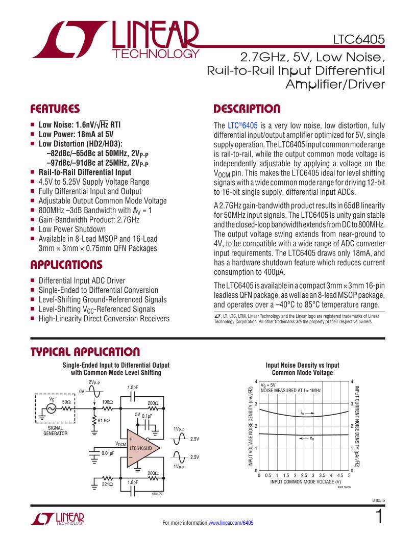
SYMBOL PARAMETER CONDITIONS MIN TYP MAX UNITS
VOSDIFF Differential Offset Voltage (Input Referred) VICM = 5V (Note 12) VICM = 2.5V VICM = 0V (Note 12)
l
l
l
±1 ±0.5 ±1
±7 ±3.5 ±7
mV mV mV
∆VOSDIFF/∆T Differential Offset Voltage Drift (Input Referred) VICM = 5V (Note 12) VICM = 2.5V VICM = 0V (Note 12)
l
l
l
1.5 1 3
µV/°C µV/°C µV/°C
IB Input Bias Current (Note 6) VICM = 5V VICM = 2.5V VICM = 0V
l
–24
8 –7
–14
µA µA µA
IOS Input Offset Current (Note 6) VICM = 5V VICM = 2.5V VICM = 0V
l
±0.5 ±0.5 ±0.5
±4
µA µA µA
RIN Input Resistance Common Mode Differential Mode
230 3.5
kΩ kΩ
CIN Input Capacitance Differential 1 pF
en Differential Input Referred Noise Voltage Density f = 1MHz, Not Including RI/RF Noise
1.6 nV/√Hz
in Input Noise Current Density f = 1MHz, Not Including RI/RF Noise
2.4 pA/√Hz
enVOCM Input Referred Common Mode Output Noise Voltage Density
f = 1MHz 9.5 nV/√Hz
VICMR (Note 7) Input Signal Common Mode Range Op-Amp Inputs l V– V+ V
CMRRI (Note 8)
Input Common Mode Rejection Ratio (Input Referred) ∆VICM/∆VOSDIFF
VICM from 0V to 5V l 50 75 dB
CMRRIO (Note 8)
Output Common Mode Rejection Ratio (Input Referred) ∆VOCM/∆VOSDIFF
VOCM from 0.5V to 3.9V l 50 75 dB
PSRR (Note 9)
Differential Power Supply Rejection (∆VS/∆VOSDIFF)
VS = 4.5V to 5.25V l 50 75 dB
PSRRCM (Note 9)
Output Common Mode Power Supply Rejection (∆VS/∆VOSCM)
VS = 4.5V to 5.25V l 55 70 dB
GCM Common Mode Gain (∆VOUTCM/∆VOCM) VOCM from 0.5V to 3.9V l 1 V/V
∆GCM Common Mode Gain Error 100 • (GCM – 1) VOCM from 0.5V to 3.9V l ±0.25 ±0.8 %
BAL Output Balance (∆VOUTCM/∆VOUTDIFF) ∆VOUTDIFF = 2V Single-Ended Input Differential Input
l
l
–60 –65
–40 –40
dB dB
VOSCM Common Mode Offset Voltage (VOUTCM – VOCM) l ±6 ±15 mV
∆VOSCM/∆T Common Mode Offset Voltage Drift l 20 µV/°C
VOUTCMR (Note 7)
Output Signal Common Mode Range (Voltage Range for the VOCM Pin)
l 0.5 3.9 V
RINVOCM Input Resistance, VOCM Pin l 13 19 25 kΩ
VOCM Self-Biased Voltage at the VOCM Pin VOCM = Open l 2.35 2.5 2.65 V
VOUT Output Voltage, High, +OUT/–OUT Pins IL = 0 IL = –5mA
l
l
3.9 3.85
4 3.95
V V
Output Voltage, Low, +OUT/–OUT Pins IL = 0 IL = 5mA
l
l
0.3 0.42
0.45 0.54
V V
ISC Output Short-Circuit Current, +OUT/–OUT Pins (Note 10)
l ±40 ±60 mA
Dc electrical characteristics The l denotes the specifications which apply over the full operating temperature range, otherwise specifications are at TA = 25°C. V+ = 5V, V– = 0V, VCM = VOCM = VICM = 2.5V, VSHDN = open, circuit component values in Figure 1 used, unless otherwise noted. VS is defined as (V+ – V–). VOUTCM is defined as (V+OUT + V–OUT)/2. VICM is defined as (V+IN + V–IN)/2. VOUTDIFF is defined as (V+OUT – V–OUT).

LTC6405
46405fb
For more information www.linear.com/6405
SYMBOL PARAMETER CONDITIONS MIN TYP MAX UNITS
AVOL Large-Signal Open Loop Voltage Gain 90 dB
VS Supply Voltage Range l 4.5 5.25 V
IS Supply Current l 18 23 mA
ISHDN Supply Current in Shutdown VSHDN = 0V l 0.4 1 mA
RSHDN SHDN Pull-Up Resistor VSHDN = 0V to 0.5V l 30 50 70 kΩ
VIL SHDN Input Logic Low l 1.25 1.8 V
VIH SHDN Input Logic High l 2 2.55 V
tON Turn-On Time 200 ns
tOFF Turn-Off Time 50 ns
ac electrical characteristics The l denotes the specifications which apply over the full operating temperature range, otherwise specifications are at TA = 25°C. V+ = 5V, V– = 0V, VCM = VOCM = VICM = 2.5V, VSHDN = open, RLOAD = 400Ω, circuit component values in Figure 2 used, unless otherwise noted. VS is defined as (V+ – V–). VICM is defined as (V+IN + V–IN)/2. VOUTDIFF is defined as (V+OUT – V–OUT).
SYMBOL PARAMETER CONDITIONS MIN TYP MAX UNITS
SR Slew Rate Differential Output 690 V/µS
GBW Gain-Bandwidth Product fTEST = 27MHz 2.7 GHz
f–3dB –3dB Frequency (See Figure 2) QFN Package MSOP Package
500 400
800 750
MHz MHz
50MHz Distortion Differential Input, VOUTDIFF = 2VP-P (Note 13)
VOCM = 2.5V, VS = 5V 2nd Harmonic 3rd Harmonic
l
–80 –64
–53
dBc dBc
VOCM = 2.5V, VS = 5V, RLOAD = 800Ω 2nd Harmonic 3rd Harmonic
–82 –66
dBc dBc
VOCM = 2.5V, VS = 5V, RLOAD = 800Ω, RI = RF = 499Ω 2nd Harmonic 3rd Harmonic
–82 –64
dBc dBc
50MHz Distortion Single-Ended Input, VOUTDIFF = 2VP-P (Note 13)
VOCM = 2.5V, VS = 5V, RLOAD = 800Ω, RI = RF = 499Ω 2nd Harmonic 3rd Harmonic
–72 –77
dBc dBc
3rd-Order IMD at 49.5MHz, 50.5MHz VOUTDIFF = 2VP-P Envelope, RLOAD = 800Ω
–63 dBc
Equivalent OIP3 at 50MHz (Note 11) RLOAD = 800Ω 35.5 dBm
tS Settling Time VOUTDIFF = 2V Step 1% Settling 0.1% Settling
6
11
ns ns
NF Noise Figure at 50MHz Shunt-Terminated to 50Ω, RS = 50Ω ZIN = 200Ω (RI = 100Ω, RF = 300Ω)
14.4 7.5
dB dB
Dc electrical characteristics The l denotes the specifications which apply over the full operating temperature range, otherwise specifications are at TA = 25°C. V+ = 5V, V– = 0V, VCM = VOCM = VICM = 2.5V, VSHDN = open, circuit component values in Figure 1 used, unless otherwise noted. VS is defined as (V+ – V–). VOUTCM is defined as (V+OUT + V–OUT)/2. VICM is defined as (V+IN + V–IN)/2. VOUTDIFF is defined as (V+OUT – V–OUT).

LTC6405
56405fb
For more information www.linear.com/6405
Note 1: Stresses beyond those listed under Absolute Maximum Ratings may cause permanent damage to the device. Exposure to any Absolute Maximum Rating condition for extended periods may affect device reliability and lifetime.Note 2: Input pins (+IN, –IN, VOCM, SHDN and VTIP) are protected by steering diodes to either supply. If the inputs should exceed either supply voltage, the input current should be limited to less than 10mA. In addition, the inputs +IN, –IN are protected by a pair of back-to-back diodes. If the differential input voltage exceeds 1.4V, the input current should be limited to less than 10mA. Note 3: A heat sink may be required to keep the junction temperature below the Absolute Maximum Rating when the output is shorted indefinitely. Note 4: The LTC6405C/LTC6405I are guaranteed functional over the operating temperature range –40°C to 85°C.Note 5: The LTC6405C is guaranteed to meet specified performance from 0°C to 70°C. The LTC6405C is designed, characterized, and expected to meet specified performance from –40°C to 85°C but is not tested or QA sampled at these temperatures. The LTC6405I is guaranteed to meet specified performance from –40°C to 85°C.Note 6: Input bias current is defined as the average of the input currents flowing into the inputs (–IN, and +IN). Input Offset current is defined as the difference between the input currents (IOS = IB+ – IB–).Note 7: Input common mode range is tested using the test circuit of Figure 1 by taking 3 measurements of differential gain with a ±1VDC differential output with VICM = 0V; VICM = 2.5V; VICM = 5V, verifying that the differential gain has not deviated from the VICM = 2.5V case by more than 0.5%, and that the common mode offset (VOSCM) has not deviated from the common mode offset at VICM = 2.5V by more than ±35mV.The voltage range for the output common mode range is tested using the test circuit of Figure 1 by applying a voltage on the VOCM pin and testing at both VOCM = 2.5V and at the Electrical Characteristics table limits to verify that the common mode offset (VOSCM) has not deviated by more than ±20mV from the VOCM = 2.5V case.
Note 8: Input CMRR is defined as the ratio of the change in the input common mode voltage at the pins +IN or –IN to the change in differential input referred voltage offset. Output CMRR is defined as the ratio of the change in the voltage at the VOCM pin to the change in differential input referred voltage offset. This specification is strongly dependent on feedback ratio matching between the two outputs and their respective inputs, and it is difficult to measure actual amplifier performance. (See the “Effects of Resistor Pair Mismatch” in the Applications Information section of this data sheet.) For a better indicator of actual amplifier performance independent of feedback component matching, refer to the PSRR specification.Note 9: Differential Power Supply Rejection (PSRR) is defined as the ratio of the change in supply voltage to the change in differential input referred voltage offset. Common mode power supply rejection (PSRRCM) is defined as the ratio of the change in supply voltage to the change in the common mode offset, VOUTCM – VOCM.Note 10: Extended operation with the output shorted may cause the junction temperature to exceed the 150°C limit.Note 11: Because the LTC6405 is a feedback amplifier with low output impedance, a resistive load is not required when driving an ADC. Therefore, typical output power can be very small in many applications. In order to compare the LTC6405 with “RF style” amplifiers that require 50Ω load, the output voltage swing is converted to dBm as if the outputs were driving a 50Ω load. For example, 2VP-P output swing is equal to 10dBm using this convention.Note 12: Includes offset/drift induced by feedback resistors mismatch. See the Applications Information section for more details.Note 13: QFN package only—refer to datasheet curves for MSOP package numbers.
electrical characteristics

LTC6405
66405fb
For more information www.linear.com/6405
typical perForMance characteristics
Supply Current vs Supply Voltage
Supply Current vs SHDN Voltage
Shutdown Supply Current vs Supply Voltage
Differential Input Referred Offset Voltage vs Temperature
Differential Input Referred Offset Voltage vs Input Common Mode Voltage
Common Mode Offset Voltage vs Temperature
TEMPERATURE (°C)–50
–1.0
DIFF
EREN
TIAL
VOS
(mV)
–0.6
–0.2
0.2
–25 0 25 50 75
0.6
1.0
–0.8
–0.4
0
0.4
0.8
100
6405 G01
VS = 5VVOCM = 2.5VVICM = 2.5VRI = RF = 200ΩFIVE REPRESENTATIVE UNITS
INPUT COMMON MODE VOLTAGE (V)
–1.0
DIFF
EREN
TIAL
VOS
(V)
–0.6
–0.2
0.2
0.6
1.0
–0.8
–0.4
0
0.4
0.8
6405 G02
VS = 5VVOCM = 2.5VRI = RF = 200Ω
0.1% FEEDBACK NETWORKRESISTORS REPRESENT-ATIVE UNIT
0 3.51 20.5 4.51.5 2.5 43 5
TA = –40°CTA = 0°CTA = 25°CTA = 70°CTA = 85°C
TEMPERATURE (°C)–50
2
COM
MON
MOD
E OF
FSET
VOL
TAGE
(mV)
4
6
8
–25 0 25 50 75
9
3
5
7
100
6405 G03
VS = 5VVOCM = 2.5VVICM = 2.5VFIVE REPRESENTATIVE UNITS
SUPPLY VOLTAGE (V)6405 G04
TOTA
L SU
PPLY
CUR
RENT
(mA)
20
15
10
5
02 3.530.5 1 1.5 2.50 4.54 5 5.5
VSHDN = OPEN
TA = –40°CTA = 0°CTA = 25°CTA = 70°CTA = 85°C
SHDN VOLTAGE (V)6405 G05
TOTA
L SU
PPLY
CUR
RENT
(mA)
20
15
10
5
02 3.530.5 1 1.5 2.50 4.54 5
VS = 5V
TA = –40°CTA = 0°CTA = 25°CTA = 70°CTA = 85°C
SUPPLY VOLTAGE (V)6405 G06
SHUT
DOW
N SU
PPLY
CUR
RENT
(µA)
600
500
300
100
400
200
02 3.530.5 1 1.5 2.50 4.54 5 5.5
VSHDN = V–
TA = –40°CTA = 0°CTA = 25°CTA = 70°CTA = 85°C

LTC6405
76405fb
For more information www.linear.com/6405
typical perForMance characteristics
Input Noise Density vs Frequency
Input Noise Density vs Input Common Mode Voltage
Differential Slew Rate vs Temperature
Differential Output Impedance vs Frequency
CMRR vs Frequency
Differential PSRR vs Frequency
TEMPERATURE (°C)–50
600
SLEW
RAT
E (V
/µs)
640
680
–25 0 25 50 75
720
620
660
700
100
6405 G09
VS = 5V
FREQUENCY (MHz)6405 G11
CMRR
(dB)
VS = 5VVOCM = 2.5VRI = RF = 200Ω, CF = 1.8pF0.1% FEEDBACK NETWORK RESISTORS
90
80
20
30
40
50
60
70
1 10010 1000 2000FREQUENCY (MHz)
6405 G10
OUTP
UT IM
PEDA
NCE
(Ω)
VS = 5VRI = RF = 200Ω
1000
0.01
0.1
1
10
100
1 10010 1000 2000FREQUENCY (MHz)
6405 G12
PSRR
(dB)
VS = 5V80
70
10
20
30
40
50
60
1 10010 1000 2000
FREQUENCY (Hz)1k 100k 10M1M100 10k
6405 G07
1
10
100
1
10
100VS = 5VVICM = 2.5V
in
enINPU
T VO
LTAG
E NO
ISE
DENS
ITY
(nV/
Hz)
INPUT CURRENT NOISE DENSITY (pA/ Hz)
6405 G08
2 3.530.5 1 1.5 2.50 4.54 5
4
3
2
1
0
4
3
2
1
0
VS = 5VNOISE MEASURED AT f = 1MHz
in
enIN
PUT
VOLT
AGE
NOIS
E DE
NSIT
Y (n
V/ H
z)
INPUT CURRENT NOISE DENSITY (pA/ Hz)
INPUT COMMON MODE VOLTAGE (V)
LTC6405
86405fb
For more information www.linear.com/6405
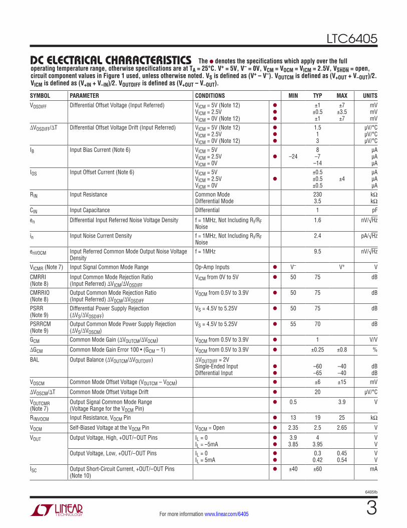
Frequency Response vs Closed Loop Gain
Frequency Response vs Load Capacitance
Frequency Response vs Input Common Mode Voltage
typical perForMance characteristics
AV = 10AV = 5
AV = 20
AV = 100
AV = 2AV = 1
FREQUENCY (MHz)
6405 G16
GAIN
(dB)
VS = 5VVOCM = VICM = 2.5VRLOAD = 400Ω
50
40
30
20
10
0
–50
–40
–30
–20
–10
1 10010 1000 2000
AV (V/V) CF (pF)RI (Ω) RF (Ω)
1251020100
200200200200200200
2004001k2k4k20k
1.81.50.60.200
FREQUENCY (MHz)6405 G17
GAIN
(dB)
VS = 5VVOCM = VICM = 2.5VRLOAD = 400ΩRI = RF = 200Ω, CF = 1.8pFCAPACITOR VALUES ARE FROM EACHOUTPUT TO GROUND.NO SERIES RESISTORS ARE USED.
30
20
10
0
–60
–50
–40
–30
–20
–10
CL = 0pFCL = 2pFCL = 3pFCL= 4.7pFCL = 10pF
1 10010 1000 2000FREQUENCY (MHz)
6405 G18
GAIN
(dB)
VS = 5VVOCM = 2.5VRLOAD = 400ΩRI = RF = 200Ω, CF = 1.8pF
10
5
0
–5
–40
–35
–30
–20
–10
–25
–15
VICM = 0VVICM = 0.5VVICM = 1.25VVICM = 2.5VVICM = 4VVICM = 5V
1 10010 1000 2000
Small Signal Step Response
Large Signal Step Response
Overdriven Output Transient Response
6405 G1310ns/DIV
20m
V/DI
V
+OUT
–OUT
VS = 5VVOCM = VICM = 2.5VRLOAD = 400Ω
RI = RF = 200ΩCF = 1.8pFCL = 0pF
6405 G1410ns/DIVVS = 5VRLOAD = 400ΩVIN = 2VP-P, DIFFERENTIAL
+OUT
–OUT0.
2V/D
IV
100ns/DIV
VOLT
AGE
(V) 3.0
3.5
4.0
2.5
2.0
0.5
0
1.5
4.5
1.0
6405 G15
VS = 5VVOCM = 2.5VRLOAD = 400Ω TO GROUND PER OUTPUT
–OUT
+OUT
(QFN Package)

LTC6405
96405fb
For more information www.linear.com/6405
Harmonic Distortion vs Frequency
Harmonic Distortion vs Input Common Mode Voltage
Harmonic Distortion vs Input Amplitude
FREQUENCY (MHz)1
–120
DIST
ORTI
ON (d
Bc)
–110
–100
–80
–60
10 100
–30
–40
–90
–70
–50
6405 G19
VS = 5VVOCM = VICM = 2.5VVTIP = OPEN (2.8V)RLOAD = 800Ω, VOUTDIFF = 2VP-PDIFFERENTIAL INPUTS
HD3 RI = RF = 200Ω
HD3 RI = RF = 499Ω
HD2 RI = RF = 499Ω
HD2 RI = RF = 200Ω
INPUT COMMON MODE VOLTAGE (V)6405 G20
DIST
ORTI
ON (d
Bc)
VS = 5VVOCM = 2.5VVTIP = OPEN (2.8V)fIN = 50MHz
RLOAD = 800ΩVOUTDIFF = 2VP-P DIFFERENTIAL INPUTS
–40
–50
–60
–70
–80
–90
–100 0 32.521.5 54.543.510.5
HD2
HD3 RI = RF = 200Ω
RI = RF = 499Ω
RI = RF = 200Ω
RI = RF = 499Ω
INPUT AMPLITUDE (dBm)6405 G21
DIST
ORTI
ON (d
Bc)
VS = 5VVOCM = VICM = 2.5VVTIP = OPEN (2.8V)fIN = 50MHzRLOAD = 800ΩRI = RF = 200ΩDIFFERENTIAL INPUTS
HD3
HD2
–40
–50
–60
–70
–80
–90
–100–2 86420–4
(0.4VP-P)10
(2VP-P)
typical perForMance characteristics
Harmonic Distortion vs Frequency
Harmonic Distortion vs Input Common Mode Voltage
Harmonic Distortion vs Input Amplitude
Intermodulation Distortion vs Frequency
Intermodulation Distortion vs Input Common Mode Voltage
Intermodulation Distortion vs Input Amplitude
INPUT COMMON MODE VOLTAGE (V)6405 G23
DIST
ORTI
ON (d
Bc)
VS = 5VVOCM = 2.5VVTIP = 2.35VfIN = 50MHz
RLOAD = 800ΩRI = RF = 499ΩVOUTDIFF = 2VP-PSINGLE-ENDED INPUT
–40
–50
–60
–70
–80
–90
–100 0 32.521.5 54.543.510.5
HD2
HD3
FREQUENCY (MHz)6405 G22
DIST
ORTI
ON (d
Bc)
VS = 5VVOCM = VICM = 2.5VVTIP = 2.35V
RLOAD = 800ΩVOUTDIFF = 2VP-PSINGLE-ENDED INPUT
–30
–40
–50
–60
–70
–80
–90
–110
–100
HD2, RI = RF = 200ΩHD2, RI = RF = 499ΩHD3, RI = RF = 200ΩHD3, RI = RF = 499Ω
1 10010
INPUT COMMON MODE VOLTAGE (V)6405 G26
THIR
D OR
DER
IMD
(dBc
)
VS = 5VVOCM = 2.5VVTIP = OPEN (2.8V)fIN = 50MHzRLOAD = 800ΩRI = RF = 200Ω2 TONES, 1MHz TONE SPACING, 2VP-P COMPOSITE DIFFERENTIAL INPUTS
–40
–50
–60
–70
–80
–90
–100 0 32.521.5 54.543.510.5
INPUT AMPLITUDE (dBm)6405 G24
DIST
ORTI
ON (d
Bc)
VS = 5VVOCM = VICM = 2.5VVTIP = 2.35VfIN = 50MHzRLOAD = 800ΩRI = RF = 499ΩSINGLE-ENDED INPUT
HD2
HD3
–40
–50
–60
–70
–80
–90
–100–2 86420–4
(0.4VP-P)10
(2VP-P)
INPUT AMPLITUDE (dBm)6405 G27
THIR
D OR
DER
IMD
(dBc
)
VS = 5VVOCM = VICM = 2.5VVTIP = OPEN (2.8V)fIN = 50MHzRLOAD = 800ΩRI = RF = 200Ω2 TONES, 1MHz TONE SPACINGDIFFERENTIAL INPUTS
–40
–50
–60
–70
–80
–90
–100–2 86420–4
(0.4VP-P)10
(2VP-P)FREQUENCY (MHz)6405 G25
THIR
D OR
DER
IMD
(dBc
)
VS = 5VVOCM = VICM = 2.5VVTIP = OPEN (2.8V)RLOAD = 800ΩRI = RF = 200Ω2 TONES, 1MHz TONE SPACING, 2VP-P COMPOSITEDIFFERENTIAL INPUTS
–30
–40
–50
–60
–70
–80
–90
–110
–100
1 10010
(QFN Package)

LTC6405
106405fb
For more information www.linear.com/6405
typical perForMance characteristics
Harmonic Distortion vs FrequencyHarmonic Distortion vs Input Amplitude
Frequency Response vs Load Capacitance Harmonic Distortion vs Frequency
Harmonic Distortion vs Input Amplitude
FREQUENCY (MHz)6405 G28
GAIN
(dB)
VS = 5VVOCM = VICM = 2.5VRLOAD = 400ΩRI = RF = 300Ω, CF = 1pFCAPACITOR VALUES ARE FROM EACHOUTPUT TO GROUND.NO SERIES RESISTORS ARE USED.
30
20
10
0
–50
–40
–30
–20
–10
CL = 10pF
1 10010 1000 2000
CL = 0pF
FREQUENCY (MHz)6405 G29
DIST
ORTI
ON (d
Bc)
VS = 5VVOCM = VICM = 2.5VVTIP = OPEN (2.8V)RLOAD = 800ΩRI = RF = 300ΩVOUTDIFF = 2VP-PDIFFERENTIAL INPUTS
–30
–40
–50
–60
–70
–80
–90
–110
–100
HD3
HD2
1 10010INPUT AMPLITUDE (dBm)
6405 G30
DIST
ORTI
ON (d
Bc)
VS = 5VVOCM = VICM = 2.5VVTIP = OPEN (2.8V)fIN = 50MHzRLOAD = 800ΩRI = RF = 300ΩDIFFERENTIAL INPUTS HD2
HD3
–40
–50
–60
–70
–80
–90
–100–2 86420–4
(0.4VP-P)10
(2VP-P)
FREQUENCY (MHz)6405 G31
DIST
ORTI
ON (d
Bc)
VS = 5VVOCM = VICM = 2.5VVTIP = OPEN (2.8V)RLOAD = 800ΩRI = RF = 300ΩVOUTDIFF = 2VP-PSINGLE-ENDED INPUT
–30
–40
–50
–60
–70
–80
–90
–110
–100HD3
HD2
1 10010INPUT AMPLITUDE (dBm)
6405 G32
DIST
ORTI
ON (d
Bc) HD2
HD3
–40
–50
–60
–70
–80
–90
–100–2 86420–4
(0.4VP-P)10
(2VP-P)
VS = 5VVOCM = VICM = 2.5VVTIP = OPEN (2.8V)fIN = 50MHzRLOAD = 800Ω
RI = RF = 300ΩSINGLE-ENDED INPUT
(MSOP Package)

LTC6405
116405fb
For more information www.linear.com/6405
pin FunctionsVOCM (Pin 2/Pin 4): Output Common Mode Reference Voltage. The voltage on VOCM sets the output common mode voltage level (which is defined as the average of the voltages on the +OUT and –OUT pins). The VOCM voltage is internally set by a resistive divider between the supplies, developing a default voltage potential of 2.5V with a 5V supply. The VOCM pin can be over-driven by an external voltage capable of driving the 19kΩ Thevenin equivalent impedance presented by the pin. The VOCM pin should be bypassed with a high quality ceramic bypass capacitor of at least 0.01µF, to minimize common mode noise from being converted to differential noise by impedance mismatches both externally and internally to the IC.
V+ (Pin 3/Pins 2, 10, 11):
V– (Pin 6/Pins 3, 9, 12):
Power Supply Pins. It is critical that close attention be paid to supply bypassing. For single supply applications, it is recommended that a high quality 0.1µF surface mount ceramic bypass capacitor be placed between V+ and V– with direct short connections. In addition, V– should be tied directly to a low impedance ground plane with minimal routing. For dual (split) power supplies, it is recommended that additional high quality, 0.1µF ceramic capacitors are used to bypass V+ to ground and V– to ground, again with minimal routing. For driving large loads (<200Ω), additional bypass capacitance may be needed for optimal performance. Keep in mind that small geometry (e.g., 0603 or smaller) surface mount ceramic capacitors have a much higher self resonant frequency than do leaded capacitors, and perform best in high speed applications.
+OUT, –OUT (Pins 4, 5/Pins 7, 14): Unfiltered Output Pins. Besides driving the feedback network, each pin can drive an additional 50Ω to ground with typical short
circuit current limiting of ±60mA. Each amplifier output is designed to drive a load capacitance of 5pF. Larger capacitive loads should be decoupled with at least 15Ω resistors from each output.
VTIP (Pin 5) QFN Only: This pin can normally be left float-ing. It determines which pair of input transistors (NPN or PNP or both) is sensing the input signal. The VTIP pin is set by an internal resistive divider between the supplies, developing a default 2.8V voltage with a 5V supply. VTIP has a Thevenin equivalent resistance of approximately 17k and can be over-driven by an external voltage. The VTIP pin should be bypassed with a high quality ceramic bypass capacitor of at least 0.01µF. See the Applications Information section for more details.
SHDN (Pin 7/Pin 1): When SHDN is floating or directly tied to V+, the LTC6405 is in the normal (active) operating mode. When the SHDN pin is connected to V–, the LTC6405 enters into a low power shutdown state with Hi-Z outputs.
+IN, –IN (Pins 8, 1/Pins 15, 6): Noninverting and Inverting Input Pins of the Amplifier, Respectively. For best perfor-mance, it is highly recommended that stray capacitance be kept to an absolute minimum by keeping printed circuit connections as short as possible.
+OUTF, –OUTF (Pins 8, 13) QFN Only: Filtered Output Pins. These pins have a series RC network (R = 50Ω, C = 3.75pF) connected between the filtered and unfiltered outputs. See the Applications Information section for more details.
NC (Pin 16) QFN Only: No Connection. This pin is not connected internally.
Exposed Pad (Pin 9/Pin 17): Tie the bottom pad to V–. If split supplies are used, DO NOT tie the pad to ground.
(MSOP/QFN)

LTC6405
126405fb
For more information www.linear.com/6405
V+50Ω
1.25pF
1.25pF
1.25pF
50Ω
V–
V+
V–
–
+
1
5VTIP
6–IN
7+OUT
8+OUTF
16NC
15+IN
14–OUT
13–OUTF
2V+
3V–
V+ V+
V+V–
4VOCM
12V–
6405 BD02
11V+
10V+
9
V–
V+
V–
V–
V–
SHDN
37k
37k30k
38k
block DiagraMsLTC6405 Block Diagram/Pinout in MSOP Package
LTC6405 Block Diagram/Pinout in QFN Package
V+
V–
V+
V–
–
+
1–IN
2VOCM
3V+
V+
4+OUT
8+IN
7 6V–
V–
5–OUT
37k
37k
6405 BD01
SHDN

LTC6405
136405fb
For more information www.linear.com/6405
applications inForMation
Figure 1. DC Test Circuit
–
+
1SHDN
5 6–IN
7+OUT
8+OUTF
16 15+IN
VTIP
NC14
–OUT13
–OUTF
V–OUTFRF
CF
V+OUTF
V–OUT
V+OUT
2V+
3V– V+
V–
V+
V–
4VOCM
VSHDN
VVOCM
VOCM
12V–
11V+
10V+
9
V–
V–
V–
V–
CF
V–
V–
6405 F01
LTC6405SHDN
0.1µF
0.01µF
VCM
RF
RI
RI
RBAL100k
RBAL100k
+
–VINP
–
+VINM
V–IN
V+IN
VOUTCMV+
0.1µFV–
0.1µF
0.1µF
0.1µF
1.25pF
1.25pF
1.25pF
0.1µF
0.01µF
50Ω
50Ω
(RI, RF : 0.1% RESISTORS)
*TO OPTIMIZE THE HIGH FREQUENCY PERFORMANCE FOR THE PIN CONFIGURATION OF THE LTC6405 IN THE SMALL MSOP PACKAGE, A FEEDBACK RESISTANCE OF AT LEAST 300Ω IS RECOMMENDED.
PACKAGE
MSOP*
QFN
DEFAULT VALUES
CF
1.0pF
1.8pF
RI
300Ω
200Ω
RF
300Ω
200Ω
Functional Description
The LTC6405 is a small outline, wideband, low noise, and low distortion fully-differential amplifier with accurate output phase balancing. The LTC6405 is optimized to drive low voltage, single-supply, differential input analog-to-digital converters (ADCs). The LTC6405 input common mode range is rail-to-rail, while the output common mode voltage is independently adjustable by applying a voltage on the VOCM pin. The output voltage swing extends from near-ground to 4V, to be compatible with a wide range of ADC converter input requirements. This makes the LTC6405 ideal for level shifting signals with a wide common mode range for driving 12-bit to 16-bit single supply, differential input ADCs. The differential output allows for twice the signal swing in low voltage systems when compared to single-ended output amplifiers. The balanced differential nature of the amplifier also provides even-order harmonic distortion cancellation, and less susceptibility to common
mode noise (like power supply noise). The LTC6405 can be used as a single ended input to differential output amplifier, or as a differential input to differential output amplifier.
The LTC6405 output common mode voltage, defined as the average of the two output voltages, is independent of the input common mode voltage, and is adjusted by apply-ing a voltage on the VOCM pin. If the pin is left open, there is an internal resistive voltage divider, which develops a potential of 2.5V (if the supply is 5V). It is recommended that a high quality ceramic cap is used to bypass the VOCM pin to a low impedance ground plane. The LTC6405’s internal common mode feedback path forces accurate output phase balancing to reduce even order harmonics, and centers each individual output about the potential set by the VOCM pin.
VOUTCM = VOCM =
V+OUT + V–OUT2

LTC6405
146405fb
For more information www.linear.com/6405
applications inForMation
Figure 2. AC Test Circuit (–3dB BW Testing)
0.01µF
–
+
1SHDN
5 6 7 8
16 15NC
14 13
2V+
3V– V+
V–
V+
V–
4VOCM
VSHDN
VVOCM
VOCM
12V–
11V+
10V+
9
V–
V–
V–
V–
V–
V–
V–
6405 F02
LTC6405SHDN
0.1µF
0.01µFRT CHOSEN SO THAT RT||RI = 100Ω
0.1µF
0.1µF
0.1µF
0.1µF
RI
RI
100Ω
100ΩRT
50ΩMINI-CIRCUITS
TCM4-19MINI-CIRCUITS
TCM4-19
V+OUT
V–OUT
V+
0.1µF
0.1µF
0.1µF
0.1µF
0.1µF
+
–VIN
• •
50Ω
••
VTIP
RT
–IN +OUT +OUTF
+IN –OUT –OUTF
V–OUTFRF
CF
V+OUTF
CF
RF
1.25pF
1.25pF
1.25pF
50Ω
50Ω
V–IN
V+IN
(RI, RF : 0.1% RESISTORS)
*TO OPTIMIZE THE HIGH FREQUENCY PERFORMANCE FOR THE PIN CONFIGURATION OF THE LTC6405 IN THE SMALL MSOP PACKAGE, A FEEDBACK RESISTANCE OF AT LEAST 300Ω IS RECOMMENDED.
PACKAGE
MSOP*
QFN
DEFAULT VALUES
CF
1.0pF
1.8pF
RI
300Ω
200Ω
RF
300Ω
200Ω
The outputs (+OUT and –OUT) of the LTC6405 are capable of swinging from close-to-ground to typically 1V below V+. They can source or sink up to approximately 60mA of current. Each output is designed to directly drive up to 5pF to ground. Higher load capacitances should be decoupled with at least 15Ω of series resistance from each output.
Input Pin Protection
The LTC6405 input stage is protected against differential input voltages which exceed 1.4V by two pairs of series diodes connected back to back between +IN and –IN. In addition, the input pins have clamping diodes to either power supply. If the input pins are over-driven, the current should be limited to under 10mA to prevent damage to the
IC. The LTC6405 also has clamping diodes to either power supply on the VOCM, VTIP and SHDN pins and if driven to voltages which exceed either supply, they too, should be current limited to under 10mA.
SHDN Pin
The SHDN pin is a CMOS logic input with a 50k internal pull-up resistor. If the pin is driven low, the LTC6405 pow-ers down with Hi-Z outputs. If the pin is left unconnected or driven high, the part is in normal active operation. Some care should be taken to control leakage currents at this pin to prevent inadvertently putting the LTC6405 into shutdown. The turn-on and turn-off time between the shutdown and active states are typically less than 1µs.

LTC6405
156405fb
For more information www.linear.com/6405
applications inForMationGeneral Amplifier Applications
As levels of integration have increased and correspond-ingly, system supply voltages decreased, there has been a need for ADCs to process signals differentially in order to maintain good signal to noise ratios. These ADCs are typically supplied from a single supply voltage which can be as low as 3V, and will have an optimal common mode input range of 1.25V or 1.5V. The LTC6405 makes interfacing to these ADCs easy, by providing both single-ended to differential conversion as well as common mode level shifting. The gain to VOUTDIFF from VINM and VINP is:
VOUTDIFF = V+OUT – V–OUT ≈
RFRI
• VINP – VINM( )
Note from the above equation, the differential output volt-age (V+OUT – V–OUT) is completely independent of input and output common mode voltages, or the voltage at the common mode pin. This makes the LTC6405 ideally suited for pre-amplification, level shifting and conversion of single ended signals to differential output signals in preparation for driving differential input ADCs.∆
Effects of Resistor Pair Mismatch
Figure 3 shows a circuit diagram which takes into consid-eration that real world resistors will not match perfectly. Assuming infinite open loop gain, the differential output relationship is given by the equation:
VOUTDIFF = V+OUT – V–OUT ≅ RFRI
• VINDIFF +
∆bbAVG
• VICM –∆b
bAVG• VOCM
where:
RF is the average of RF1, and RF2, and RI is the average of RI1, and RI2.
bAVG is defined as the average feedback factor from the outputs to their respective inputs:
bAVG = 1
2•
RI1RI1 + RF1
+RI2
RI2 + RF2
∆b is defined as the difference in feedback factors:
∆b = RI2
RI2 +RF2–
RI1RI1 +RF1
VICM is defined as the average of the two input voltages VINP and VINM (also called the input common mode voltage):
VICM = 1
2• VINP + VINM( )
and VINDIFF is defined as the difference of the input voltages:
VINDIFF = VINP – VINM
VOCM is defined as the average of the two output voltages V+OUT and V–OUT:
VOCM =
V+OUT + V−OUT2
When the feedback ratios mismatch (∆b), common mode to differential conversion occurs.
Setting the differential input to zero (VINDIFF = 0), the de-gree of common mode to differential conversion is given by the equation:
VOUTDIFF = V+OUT – V–OUT ≈ VICM – VOCM( ) •
∆bbAVG
Figure 3. Real-World Application with Feedback Resistor Pair Mismatch
–
+
RF2V–OUT
V+OUT
VVOCM VOCM
6405 F03
RF1
RI2
RI1
+
–VINP
–
+VINM
V–IN
V+IN
LTC6405
166405fb
For more information www.linear.com/6405
applications inForMationIn general, the degree of feedback pair mismatch is a source of common mode to differential conversion of both signals and noise. Using 1% resistors or better will mitigate most problems, and will provide about 34dB worst case of common mode rejection. Using 0.1% resistors will provide about 54dB of common mode rejection. A low impedance ground plane should be used as a reference for both the input signal source and the VOCM pin. Bypassing the VOCM with a high quality 0.1µF ceramic capacitor to this ground plane will further help prevent common mode signals from being converted to differential signals.
There may be concern on how feedback factor mismatch affects distortion. Feedback factor mismatch from using 1% resistors or better, has a negligible effect on distortion. However, in single supply level shifting applications where there is a voltage difference between the input common mode voltage and the output common mode voltage, resistor mismatch can make the apparent voltage offset of the amplifier appear worse than specified.
The apparent input referred offset induced by feedback factor mismatch is derived from the above equation:
VOSDIFF(APPARENT) ≈ (VICM – VOCM) • ∆b
Using the LTC6405 in a single supply application on a single 5V supply with 1% resistors, and the input common mode grounded, with the VOCM pin biased at 2.5V, the worst case DC offset can induce 25mV of apparent offset voltage. With 0.1% resistors, the worst case apparent offset reduces to 2.5mV.
Input Impedance and Loading Effects
The input impedance looking into the VINP or VINM input of Figure 1 depends on whether or not the sources VINP and VINM are fully differential or not. For balanced input sources (VINP = –VINM), the input impedance seen at either input is simply:
RINP = RINM = RI
For single ended inputs, because of the signal imbalance at the input, the input impedance actually increases over
the balanced differential case. The input impedance looking into either input is:
RINP = RINM =RI
1–12
•RF
RI + RF
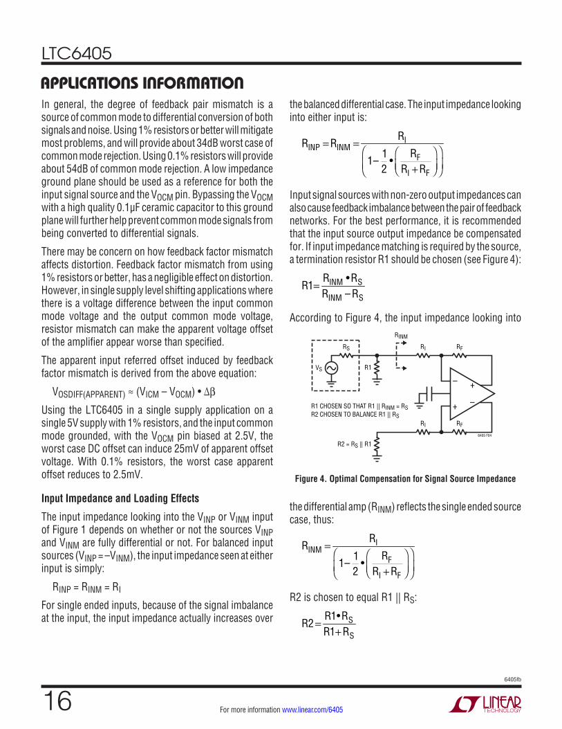
Input signal sources with non-zero output impedances can also cause feedback imbalance between the pair of feedback networks. For the best performance, it is recommended that the input source output impedance be compensated for. If input impedance matching is required by the source, a termination resistor R1 should be chosen (see Figure 4):
R1=
RINM •RSRINM –RS
According to Figure 4, the input impedance looking into
Figure 4. Optimal Compensation for Signal Source Impedance
VS
+
–
–
+
RF
RF
RI
RINM
RS
RI
R2 = RS || R1
R1 CHOSEN SO THAT R1 || RINM = RSR2 CHOSEN TO BALANCE R1 || RS
R1
6405 F04
the differential amp (RINM) reflects the single ended source case, thus:
RINM =RI
1–12
•RF
RI + RF
R2 is chosen to equal R1 || RS:
R2 =
R1•RSR1+ RS

LTC6405
176405fb
For more information www.linear.com/6405
–
+
RFV–OUT
V+OUT
VVOCM VOCM
6405 F05
RF
RI
RI
+
–VINP
+
–VCM –
+VINM
V–IN
V+IN
applications inForMationInput Common Mode Voltage Range
The LTC6405’s input common mode voltage (VICM) is defined as the average of the two input voltages, V+IN, and V–IN. At the inputs to the actual op amp, the range extends from V– to V+. This makes it easy to interface to a wide range of common mode signals, from ground referenced to VCC referenced signals. Moreover, due to external resistive divider action of the gain and feedback resistors, the effective range of signals that can be processed is even wider. The input common mode range at the op amp inputs depends on the circuit configuration (gain), VOCM and VCM (refer to Figure 5). For fully differential input applications, where VINP = –VINM, the common mode input is approximately:
VICM =V+IN + V–IN
2≈ VOCM •
RIRI + RF
+
VCM •RF
RF + RI
Figure 5. Circuit for Common Mode Range
Manipulating the Rail-to-Rail Input Stage with VTIP
To achieve rail-to-rail input operation, the LTC6405 features an NPN input stage in parallel with a PNP input stage. When the input common mode voltage is near V+, the NPNs are active while the PNPs are off. When the input common mode is near V–, the PNPs are active while the NPNs are off. At some range in the middle, both input stages are active. This ‘hand-off’ operation happens automatically.
In the QFN package, a special pin, VTIP, is made available that can be used to manipulate the ‘hand-off’ operation between the NPN and PNP input stages. By default, the VTIP pin is internally biased by an internal resistive divider between the supplies, developing a default 2.8V voltage with a 5V supply. If desired, VTIP can be over-driven by an external voltage (the Thevenin equivalent resistance is approximately 17k).
If VTIP is pulled closer to V–, the range over which the NPN input pair remains active is increased, while the range over which the PNP input pair is active is reduced. In applica-tions where the input common mode does not come close to V– , this mode can be used to further improve linearity beyond the specified performance (see Figure 6).
If VTIP is pulled closer to V+, the range over which the PNP input pair remains active is increased, while the range over which the NPN input pair is active is reduced. In applica-tions where the input common mode does not come close to V+, this mode can be used to further improve linearity beyond the specified performance.
With single ended inputs, there is an input signal compo-nent to the input common mode voltage. Applying only VINP (setting VINM to zero), the input common voltage is approximately:
VICM =V+IN + V–IN
2≈ VOCM •
RIRI + RF
+
VCM •RF
RF + RI
+VINP
2•
RFRF + RI
Use the equations above to check that the VICM at the op amp inputs is within range (V– to V+).
Figure 6. Manipulating VTIP to Improve Harmonic Distortion
HD2 VTIP = OPEN
HD3 VTIP = OPEN
FREQUENCY (MHz)6405 F06
DIST
ORTI
ON (d
Bc)
VS = 5VVOCM = VICM = 2.5VRLOAD = 800Ω
RI = RF = 499ΩVOUTDIFF = 2VP-P SINGLE-ENDED INPUTQFN PACKAGE
–30
–40
–50
–60
–70
–80
–90
–110
–100
1 10010
HD3 VTIP = 1V
HD2 VTIP = 1V

LTC6405
186405fb
For more information www.linear.com/6405
Output Common Mode Voltage Range
The output common mode voltage is defined as the aver-age of the two outputs:
VOUTCM = VOCM =
V+OUT + V–OUT2
The VOCM pin sets this average by an internal common mode feedback loop which internally forces VOUTCM = VOCM. The output common mode range extends from 0.5V above V– to typically 1V below V+. The VOCM voltage is internally set by a resistive divider between the supplies, developing a default voltage potential of 2.5V with a 5V supply.
In single supply applications, where the LTC6405 is used to interface to an ADC, the optimal common mode input range to the ADC is often determined by the ADC’s refer-ence. If the ADC makes a reference available for setting the input common mode voltage, it can be directly tied to the VOCM pin (as long as it is able to drive the 19kΩ Thevenin equivalent input impedance presented by the VOCM pin).
The VOCM pin should be bypassed with a high quality ceramic bypass capacitor of at least 0.01µF to filter any common mode noise rather than being converted to dif-ferential noise and to prevent common mode signals on this pin from being inadvertently converted to differential signals by impedance mismatches both externally and internally to the IC.
applications inForMationOutput Filter Considerations and Use
Filtering at the output of the LTC6405 is often desired to provide anti-aliasing or to improve signal to noise ratio. To simplify this filtering, the LTC6405 in the QFN package includes an additional pair of differential outputs (+OUTF and –OUTF) which incorporate an internal lowpass RC network with a –3dB bandwidth of 850MHz (Figure 7).
These pins each have an output resistance of 50Ω (toler-ance ±12%). Internal capacitances are 1.25pF (tolerance ±15%) to V– on each filtered output, plus an additional 1.25pF (tolerance ±15%) capacitor connected between the two filtered outputs. This resistor/capacitor combination creates filtered outputs that look like a series 50Ω resistor with a 3.75pF capacitor shunting each filtered output to AC ground, providing a –3dB bandwidth of 850MHz, and a noise bandwidth of 1335MHz. The filter cutoff frequency is easily modified with just a few external components. To increase the cutoff frequency, simply add two equal value resistors, one between +OUT and +OUTF and the other between –OUT and –OUTF (Figure 8). These resistors, in parallel with the internal 50Ω resistors, lower the overall resistance and therefore increase filter bandwidth. For example, to double the filter bandwidth, add two external 50Ω resistors to lower the series filter resistance to 25Ω. The 3.75pF of capacitance remains unchanged, so filter bandwidth doubles. Keep in mind, the series resistance also serves to decouple the outputs from load capaci-
Figure 7. LTC6405 Internal Filter Topology
–
+
7+OUT
8+OUTF
14–OUT
13–OUTF
+OUTF
–OUTF
1.25pF
1.25pF
50Ω
50Ω
1.25pF
12V–
9
V–V–
V–
6405 F07
LTC6405
FILTERED OUTPUT
Figure 8. LTC6405 Filter Topology Modified for 2x Filter Bandwidth (Two External Resistors)
–
+
7 8
14 13
12V–
9
V–V–
V–
6405 F08
LTC6405
FILTERED OUTPUT(1.7GHz)
+OUTF
–OUTF
49.9Ω
49.9Ω
1.25pF
1.25pF
50Ω
50Ω
1.25pF
+OUT +OUTF
–OUT –OUTF

LTC6405
196405fb
For more information www.linear.com/6405
applications inForMationtance. The outputs of the LTC6405 are designed to drive 5pF to ground, so care should be taken to not lower the effective impedance between +OUT and +OUTF or –OUT and –OUTF below 15Ω.
To decrease filter bandwidth, add two external capacitors, one from +OUTF to ground, and the other from –OUTF to ground. A single differential capacitor connected between +OUTF and –OUTF can also be used, but since it is being driven differentially it will appear at each filtered output as a single-ended capacitance of twice the value. To halve the filter bandwidth, for example, two 3.9pF capacitors could be added (one from each filtered output to ground). Alternatively, one 1.8pF capacitor could be added between the filtered outputs, which also halves the filter bandwidth. Combinations of capacitors could be used as well; a three capacitor solution of 1.2pF from each filtered output to ground plus a 1.2pF capacitor between the filtered outputs would also halve the filter bandwidth (Figure 9).
Noise Considerations
The LTC6405’s input referred voltage noise is 1.6nV/√Hz. Its input referred current noise is 2.4pA/√Hz. In addition to the noise generated by the amplifier, the surrounding feedback resistors also contribute noise. A noise model is shown in Figure 10. The output noise generated by both
the amplifier and the feedback components is governed by the equation:
eno =
eni • 1+RFRI
2
+ 2 • In •RF( )2 +
2 • enRI •RFRI
2
+ 2 • enRF2
A plot of this equation, and a plot of the noise generated by the feedback components for the LTC6405 is shown in Figure 11.
Figure 9. LTC6405 Filter Topology Modified for 1/2x Filter Bandwidth (Three External Capacitors)
–
+
7 8
14 13
12V–
9
V–V–
V–
6405 F09
LTC6405
FILTERED OUTPUT(425MHz)
1.25pF
1.25pF
50Ω
50Ω
1.25pF
1.2pF
1.2pF
1.2pF
+OUTF
–OUTF
+OUT +OUTF
–OUT –OUTF
Figure 10. Noise Model of the LTC6405
Figure 11. LTC6405 Output Spot Noise vs Spot Noise Contributed by Feedback Network Alone
–
+eno
2
RF
VOCM
enRI2
RF
RI
RI
enRF2
enRI2
encm2
eni2
enRF2
in+2
in–2
6405 F10
RI = RF (Ω)10
0.1
1
10
100
100 1000 10000
6405 F11
TOTAL (AMPLIFIER ANDFEEDBACK NETWORK)OUTPUT NOISE
FEEDBACK NETWORKNOISE ALONE
nV/
Hz
LTC6405
206405fb
For more information www.linear.com/6405
applications inForMationThe LTC6405’s input referred voltage noise contributes the equivalent noise of a 155Ω resistor. When the feedback network is comprised of resistors whose values are less than this, the LTC6405’s output noise is voltage noise dominant (see Figure 11):
eno ≈ eni • 1+
RFRI
Feedback networks consisting of resistors with values greater than about 200Ω will result in output noise which is resistor noise and amplifier current noise dominant.
eno ≈ 2 • In •RF( )2 + 1+
RFRI
• 4 •k • T •RF
Lower resistor values (<100Ω) always result in lower noise at the penalty of increased distortion due to increased loading of the feedback network on the output. Higher resistor values (but still less than <500Ω) will result in higher output noise, but typically improved distortion due to less loading on the output. The optimal feedback resis-tance for the LTC6405 runs in between 100Ω to 500Ω.
The differential filtered outputs +OUTF and –OUTF will have a little higher noise than the unfiltered outputs (due to the two 50Ω resistors which contribute 0.9nV/√Hz each), but can provide superior signal-to-noise due to the output noise filtering.
Layout Considerations
Because the LTC6405 is a very high speed amplifier, it is sensitive to both stray capacitance and stray inductance. In the QFN package, three pairs of power supply pins are provided to keep the power supply inductance as low as possible to prevent any degradation of amplifier 2nd harmonic performance. It is critical that close attention be paid to supply bypassing. For single supply applications it is recommended that high quality 0.1µF surface mount ceramic bypass capacitor be placed directly between each V+ and V– pin with direct short connections. The V– pins should be tied directly to a low impedance ground plane with minimal routing. For dual (split) power supplies, it is
recommended that additional high quality, 0.1µF ceramic capacitors are used to bypass V+ to ground and V– to ground, again with minimal routing. For driving large loads (<200Ω), additional bypass capacitance may be needed for optimal performance. Keep in mind that small geometry (e.g., 0603) surface mount ceramic capacitors have a much higher self resonant frequency than do leaded capacitors, and perform best in high speed applications.
Any stray parasitic capacitances to ground at the summing junctions, +IN and –IN, should be minimized. This becomes especially true when the feedback resistor network uses resistor values >500Ω in circuits with RF = RI. Always keep in mind the differential nature of the LTC6405, and that it is critical that the load impedances seen by both outputs (stray or intended), should be as balanced and symmetric as possible. This will help preserve the natural balance of the LTC6405, which minimizes the generation of even order harmonics, and improves the rejection of common mode signals and noise.
It is highly recommended that the VOCM pin be bypassed to ground with a high quality ceramic capacitor whose value exceeds 0.01µF. This will help stabilize the common mode feedback loop as well as prevent thermal noise from the internal voltage divider and other external sources of noise from being converted to differential noise due to divider mismatches in the feedback networks. It is also recommended that the resistive feedback networks be comprised of 1% resistors (or better) to enhance the output common mode rejection. This will also prevent VOCM input referred common mode noise of the common mode amplifier path (which cannot be filtered) from being converted to differential noise, degrading the differential noise performance.
Feedback factor mismatch has a weak effect on distortion. Using 1% or better resistors will limit any mismatch from impacting amplifier linearity. However, in single supply level shifting applications where there is a voltage differ-ence between the input common mode voltage and the output common mode voltage, resistor mismatch can make the apparent voltage offset of the amplifier appear worse than specified.
LTC6405
216405fb
For more information www.linear.com/6405
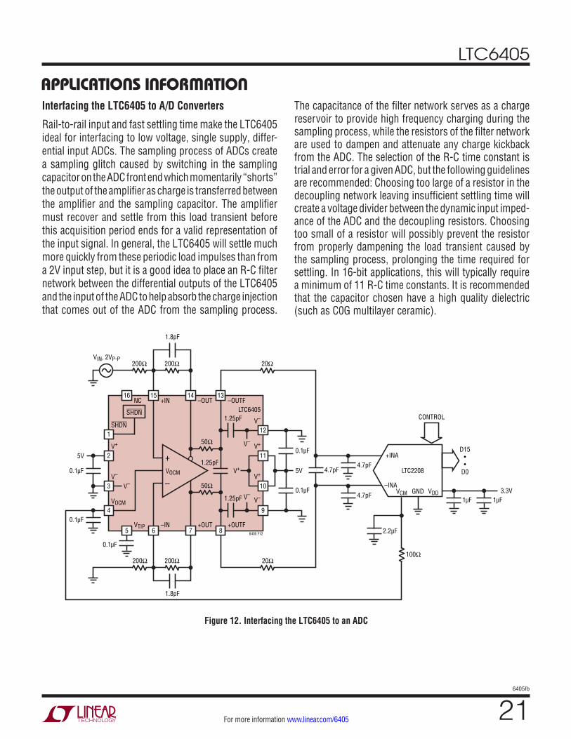
Interfacing the LTC6405 to A/D Converters
Rail-to-rail input and fast settling time make the LTC6405 ideal for interfacing to low voltage, single supply, differ-ential input ADCs. The sampling process of ADCs create a sampling glitch caused by switching in the sampling capacitor on the ADC front end which momentarily “shorts” the output of the amplifier as charge is transferred between the amplifier and the sampling capacitor. The amplifier must recover and settle from this load transient before this acquisition period ends for a valid representation of the input signal. In general, the LTC6405 will settle much more quickly from these periodic load impulses than from a 2V input step, but it is a good idea to place an R-C filter network between the differential outputs of the LTC6405 and the input of the ADC to help absorb the charge injection that comes out of the ADC from the sampling process.
The capacitance of the filter network serves as a charge reservoir to provide high frequency charging during the sampling process, while the resistors of the filter network are used to dampen and attenuate any charge kickback from the ADC. The selection of the R-C time constant is trial and error for a given ADC, but the following guidelines are recommended: Choosing too large of a resistor in the decoupling network leaving insufficient settling time will create a voltage divider between the dynamic input imped-ance of the ADC and the decoupling resistors. Choosing too small of a resistor will possibly prevent the resistor from properly dampening the load transient caused by the sampling process, prolonging the time required for settling. In 16-bit applications, this will typically require a minimum of 11 R-C time constants. It is recommended that the capacitor chosen have a high quality dielectric (such as C0G multilayer ceramic).
applications inForMation
Figure 12. Interfacing the LTC6405 to an ADC
0.1µF
–
+
1SHDN
5 6–IN
7+OUT
8+OUTF
16 15+INNC
14–OUT
13–OUTF
+INA
–INA
200Ω
2V+
3V– V+
V–
5V
VOCM
VOCM
12V–
11V+
10V+
9
V–
V–
V–
6405 F12
LTC6405
LTC2208
VIN, 2VP-P
SHDN
200Ω200Ω100Ω
200Ω
0.1µF
20Ω
20Ω
5V
4
0.1µF
0.1µF
CONTROL
GND VDDVCM
D15••
D0
0.1µF
4.7pF
4.7pF
4.7pF
3.3V1µF 1µF
VTIP
1.8pF
1.8pF
1.25pF
1.25pF
1.25pF
50Ω
50Ω
2.2µF

LTC6405
226405fb
For more information www.linear.com/6405
Attenuating and Level Shifting a Single-Ended ±5V Signal to a Differential 2VP-P Signal at a 1.25V Common Mode
LTC2207
3.3V
6405 TA03
R151.1Ω
±5V SINE WAVE(10VP-P)
CENTERED AT 0V
R251.1Ω
R3, 100Ω
R4, 100Ω
C1, 2.7pF
C2, 2.7pF
2VP-P DIFF OUTPUTLEVEL-SHIFTED TO 1.25V
VIN
R5511Ω
R6511Ω
+
–
–
+
5V
LTC6405
VCM = 1.25V2.2µF
typical application

LTC6405
236405fb
For more information www.linear.com/6405
package DescriptionPlease refer to http://www.linear.com/designtools/packaging/ for the most recent package drawings.
MSOP (MS8E) 0911 REV J
0.53 ±0.152(.021 ±.006)
SEATINGPLANE
NOTE:1. DIMENSIONS IN MILLIMETER/(INCH)2. DRAWING NOT TO SCALE3. DIMENSION DOES NOT INCLUDE MOLD FLASH, PROTRUSIONS OR GATE BURRS. MOLD FLASH, PROTRUSIONS OR GATE BURRS SHALL NOT EXCEED 0.152mm (.006") PER SIDE4. DIMENSION DOES NOT INCLUDE INTERLEAD FLASH OR PROTRUSIONS. INTERLEAD FLASH OR PROTRUSIONS SHALL NOT EXCEED 0.152mm (.006") PER SIDE5. LEAD COPLANARITY (BOTTOM OF LEADS AFTER FORMING) SHALL BE 0.102mm (.004") MAX6. EXPOSED PAD DIMENSION DOES INCLUDE MOLD FLASH. MOLD FLASH ON E-PAD SHALL NOT EXCEED 0.254mm (.010") PER SIDE.
0.18(.007)
0.254(.010)
1.10(.043)MAX
0.22 – 0.38(.009 – .015)
TYP
0.86(.034)REF
0.65(.0256)
BSC
0° – 6° TYP
DETAIL “A”
DETAIL “A”
GAUGE PLANE
1 2 3 4
4.90 ±0.152(.193 ±.006)
8
8
1
BOTTOM VIEW OFEXPOSED PAD OPTION
7 6 5
3.00 ±0.102(.118 ±.004)
(NOTE 3)
3.00 ±0.102(.118 ±.004)
(NOTE 4)
0.52(.0205)
REF
1.68(.066)
1.88(.074)
5.23(.206)MIN
3.20 – 3.45(.126 – .136)
1.68 ±0.102(.066 ±.004)
1.88 ±0.102(.074 ±.004) 0.889 ±0.127
(.035 ±.005)
RECOMMENDED SOLDER PAD LAYOUT
0.65(.0256)
BSC0.42 ±0.038
(.0165 ±.0015)TYP
0.1016 ±0.0508(.004 ±.002)
DETAIL “B”
DETAIL “B”CORNER TAIL IS PART OF
THE LEADFRAME FEATURE.FOR REFERENCE ONLY
NO MEASUREMENT PURPOSE
0.05 REF
0.29REF
MS8E Package8-Lead Plastic MSOP, Exposed Die Pad(Reference LTC DWG # 05-08-1662 Rev J)

LTC6405
246405fb
For more information www.linear.com/6405
3.00 ±0.10(4 SIDES)
RECOMMENDED SOLDER PAD PITCH AND DIMENSIONS
1.45 ±0.05(4 SIDES)
NOTE:1. DRAWING CONFORMS TO JEDEC PACKAGE OUTLINE MO-220 VARIATION (WEED-2)2. DRAWING NOT TO SCALE3. ALL DIMENSIONS ARE IN MILLIMETERS4. DIMENSIONS OF EXPOSED PAD ON BOTTOM OF PACKAGE DO NOT INCLUDE MOLD FLASH. MOLD FLASH, IF PRESENT, SHALL NOT EXCEED 0.15mm ON ANY SIDE5. EXPOSED PAD SHALL BE SOLDER PLATED6. SHADED AREA IS ONLY A REFERENCE FOR PIN 1 LOCATION ON THE TOP AND BOTTOM OF PACKAGE
PIN 1TOP MARK(NOTE 6)
0.40 ±0.10
BOTTOM VIEW—EXPOSED PAD
1.45 ± 0.10(4-SIDES)
0.75 ±0.05 R = 0.115TYP
0.25 ±0.05
1
PIN 1 NOTCH R = 0.20 TYPOR 0.25 × 45° CHAMFER
15 16
2
0.50 BSC
0.200 REF
2.10 ±0.053.50 ±0.05
0.70 ±0.05
0.00 – 0.05
(UD16) QFN 0904
0.25 ±0.050.50 BSC
PACKAGE OUTLINE
UD Package16-Lead Plastic QFN (3mm × 3mm)
(Reference LTC DWG # 05-08-1691 Rev Ø)
package DescriptionPlease refer to http://www.linear.com/designtools/packaging/ for the most recent package drawings.

LTC6405
256405fb
For more information www.linear.com/6405
Information furnished by Linear Technology Corporation is believed to be accurate and reliable. However, no responsibility is assumed for its use. Linear Technology Corporation makes no representa-tion that the interconnection of its circuits as described herein will not infringe on existing patent rights.
revision historyREV DATE DESCRIPTION PAGE NUMBER
B 02/13 Changed operating voltage upper range from 5.5V to 5.25V 1, 3, 4
Changed voltage max spec from 0.4V to 0.45V 3
(Revision history begins at Rev B)

LTC6405
266405fb
For more information www.linear.com/6405 LINEAR TECHNOLOGY CORPORATION 2012
LT 0213 REV B • PRINTED IN USALinear Technology Corporation1630 McCarthy Blvd., Milpitas, CA 95035-7417(408) 432-1900 FAX: (408) 434-0507 www.linear.com/6405
typical application
PART NUMBER DESCRIPTION COMMENTS
LT1993-2/LT1993-4/ LT1993-10
800MHz/900MHz/700MHz Low Distortion, Low Noise Differential Amplifier/ADC Driver
AV = 2V/V / AV = 4V/V / AV = 10V/V, NF = 12.3dB/14.5dB/ 12.7dB, OIP3 = 38dBm/40dBm/40dBm at 70MHz
LT1994 Low Noise, Low Distortion Fully differential Input/Output Amplifier/Driver
Low Distortion, 2VP-P , 1MHz: –94dBc, 13mA, Low Noise: 3nV/√Hz
LTC6400-8/LTC6400-14/LTC6400-20/LTC6400-26
1.8GHz Low Noise, Low Distortion, Differential ADC Driver 300MHz IF Amplifier, AV = 20dB/26dB
LTC6401-8/LTC6401-14/LTC6401-20/LTC6401-26
1.3GHz Low Noise, Low Distortion, Differential ADC Driver 140MHz IF Amplifier, AV = 20dB/26dB
LT6402-6/LT6402-12/ LT6402-20
300MHz/300MHz/300MHz Low Distortion, Low Noise Differential Amplifier/ADC Driver
AV = 6dB/AV = 12dB/AV = 20dB, NF = 18.6dB/15dB/12.4dB, OIP3 = 49dBm/43dBm/51dBm at 20MHz
LTC6404-1/ LTC6404-2/ LTC6404-4
600MHz Low Noise, Low Distortion, Differential ADC Driver 1.5nV/√Hz Noise, –90dBc Distortion at 10MHz
LTC6406 3GHz Low Noise, 3V, Rail-to-Rail Input Differential Amplifier/Driver
1.6nV/√Hz Noise, –70dBc Distortion at 50MHz, 18mA, 3V Supply
LTC6411 Low Power Differential ADC Driver/Dual Selectable Gain Amplifier
16mA Supply Current, IMD3 = –83dBC at 70MHz, AV = 1, –1, or 2
LT6600-2.5/LT6600-5/ LT6600-10/LT6600-20
Very Low Noise, Fully Differential Amplifier and 4th Order Filter
2.5MHz/5MHz/10MHz/20MHz Integrated Filter, 3V Supply, SO-8 Package
LTC6403-1 200MHz Low Noise, Low Power Differential ADC Driver –95dBc Distortion at 3MHz, 10.8mA Supply Current
DC-Coupled Level Shifting of Demodulator Output
LTC224914-BIT ADC
80MHzSAMPLECLOCK
3.3V
6405 TA02
10dBm
15nH
R910Ω
C84.7pF
C74.7pF
C64.7pF
C24.7pF
C14.7pF
RF IN900MHz–7dBm
R1010Ω
R749.9Ω
R5, 324Ω
R6, 324Ω
C5, 10pF
C4, 10pF
DIFF OUTPUT Z130Ω| |2.5pF
DC LEVEL1.5V
DC LEVEL3.8V
GAIN: 14dBINPUT NF: 11dB
OIP3: 44dBm AT 30MHzGAIN: 3dB
INPUT NF: 13dBOIP3: 31dBm
R849.9Ω
IDENTICALQ CHANNEL
5V
5pF
65Ω
5pF
65Ω
–
+
+
–
5V
LTC6405
5V
I
5V
5pF
65Ω
5pF
65Ω
5V
Q
5V
LT5575
4.7pF
LOOdBm
3.9pF
15nH
VOCM = 1.5V
VCM
relateD parts