Embed Size (px)
Citation preview
LTC4361-1/LTC4361-2
1436112fb
Typical applicaTion
DescripTion
Overvoltage/Overcurrent Protection Controller
applicaTionsn USB Protectionn Handheld Computersn Cell/Smart Phonesn MP3/MP4 Playersn Digital Cameras
n 2.5V to 5.5V Operationn Overvoltage Protection Up to 80Vn No Input Capacitor or TVS Required for Most
Applicationsn 2% Accurate 5.8V Overvoltage Thresholdn 10% Accurate 50mV Overcurrent Circuit Breakern <1µs Overvoltage Turn-Off, Gentle Shutdownn Controls N-Channel MOSFETn Adjustable Power-Up dV/dt Limits Inrush Currentn Reverse Voltage Protectionn Power Good Outputn Low Current Shutdownn Latchoff (LTC4361-1) or Auto-Retry (LTC4361-2)
After Overcurrent n Available in 8-Lead ThinSOT™ and 8-Lead
(2mm × 2mm) DFN Packages
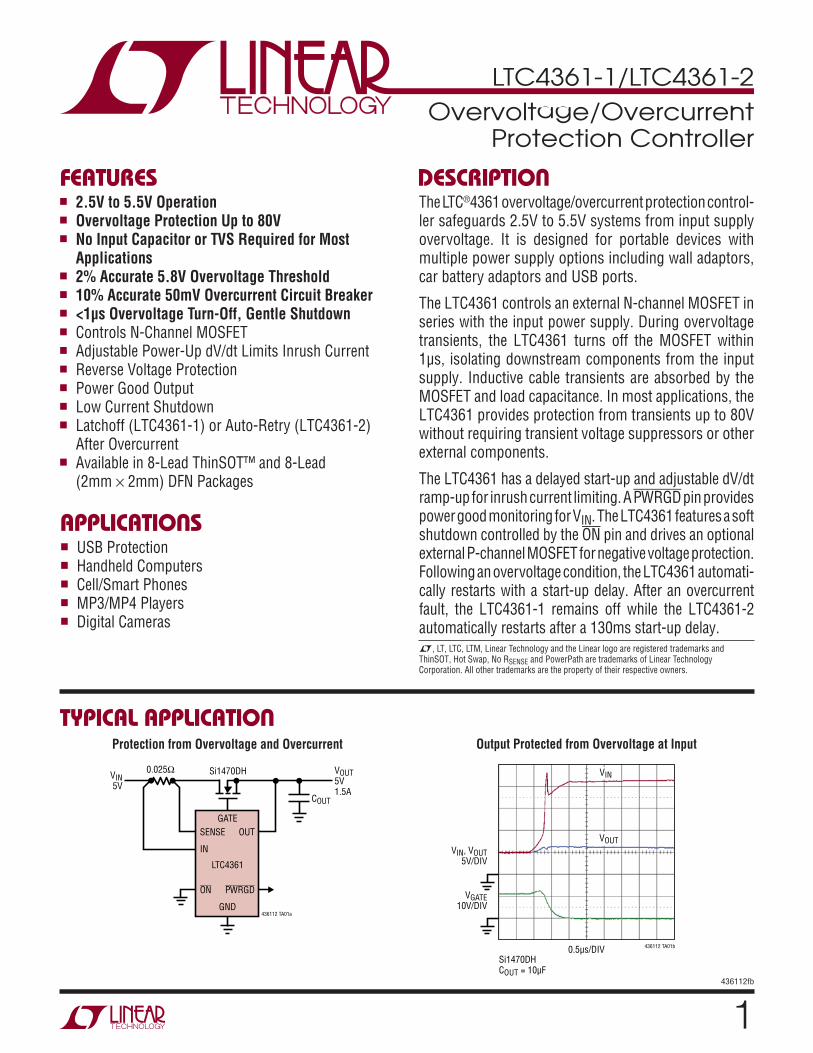
The LTC®4361 overvoltage/overcurrent protection control-ler safeguards 2.5V to 5.5V systems from input supply overvoltage. It is designed for portable devices with multiple power supply options including wall adaptors, car battery adaptors and USB ports.
The LTC4361 controls an external N-channel MOSFET in series with the input power supply. During overvoltage transients, the LTC4361 turns off the MOSFET within 1µs, isolating downstream components from the input supply. Inductive cable transients are absorbed by the MOSFET and load capacitance. In most applications, the LTC4361 provides protection from transients up to 80V without requiring transient voltage suppressors or other external components.
The LTC4361 has a delayed start-up and adjustable dV/dt ramp-up for inrush current limiting. A PWRGD pin provides power good monitoring for VIN. The LTC4361 features a soft shutdown controlled by the ON pin and drives an optional external P-channel MOSFET for negative voltage protection. Following an overvoltage condition, the LTC4361 automati-cally restarts with a start-up delay. After an overcurrent fault, the LTC4361-1 remains off while the LTC4361-2 automatically restarts after a 130ms start-up delay.L, LT, LTC, LTM, Linear Technology and the Linear logo are registered trademarks and ThinSOT, Hot Swap, No RSENSE and PowerPath are trademarks of Linear Technology Corporation. All other trademarks are the property of their respective owners.
Output Protected from Overvoltage at InputProtection from Overvoltage and Overcurrent
GATE
Si1470DH0.025Ω
SENSE
IN
436112 TA01a
VOUT5V1.5A
VIN5V
LTC4361
ON
OUT
PWRGD
GND
COUT
VGATE10V/DIV
VIN, VOUT5V/DIV
0.5µs/DIV 436112 TA01b
Si1470DHCOUT = 10µF
VOUT
VIN
FeaTures
LTC4361-1/LTC4361-2
2436112fb
Bias Supply Voltage (IN) ............................ –0.3V to 85VInput Voltages
SENSE ................................................... –0.3V to 85V OUT, ON ................................................... –0.3V to 9V
Output Voltages PWRGD .................................................... –0.3V to 9V GATE (Note 3) ........................................ –0.3V to 15V GATEP .................................................... –0.3V to 85V IN to GATEP ........................................... –0.3V to 10V
(Notes 1, 2)
orDer inFormaTionLead Free FinishTAPE AND REEL (MINI) TAPE AND REEL PART MARKING* PACKAGE DESCRIPTION TEMPERATURE RANGE
LTC4361CTS8-1#TRMPBF LTC4361CTS8-1#TRPBF LTDWN 8-Lead Plastic TSOT-23 0°C to 70°C
LTC4361CTS8-2#TRMPBF LTC4361CTS8-2#TRPBF LTFMN 8-Lead Plastic TSOT-23 0°C to 70°C
LTC4361ITS8-1#TRMPBF LTC4361ITS8-1#TRPBF LTDWN 8-Lead Plastic TSOT-23 –40°C to 85°C
LTC4361ITS8-2#TRMPBF LTC4361ITS8-2#TRPBF LTFMN 8-Lead Plastic TSOT-23 –40°C to 85°C
LTC4361HTS8-1#TRMPBF LTC4361HTS8-1#TRPBF LTDWN 8-Lead Plastic TSOT-23 –40°C to 125°C
LTC4361HTS8-2#TRMPBF LTC4361HTS8-2#TRPBF LTFMN 8-Lead Plastic TSOT-23 –40°C to 125°C
LTC4361CDC-1#TRMPBF LTC4361CDC-1#TRPBF LDWP 8-Lead (2mm × 2mm) Plastic DFN 0°C to 70°C
LTC4361CDC-2#TRMPBF LTC4361CDC-2#TRPBF LFMP 8-Lead (2mm × 2mm) Plastic DFN 0°C to 70°C
LTC4361IDC-1#TRMPBF LTC4361IDC-1#TRPBF LDWP 8-Lead (2mm × 2mm) Plastic DFN –40°C to 85°C
LTC4361IDC-2#TRMPBF LTC4361IDC-2#TRPBF LFMP 8-Lead (2mm × 2mm) Plastic DFN –40°C to 85°C
LTC4361HDC-1#TRMPBF LTC4361HDC-1#TRPBF LDWP 8-Lead (2mm × 2mm) Plastic DFN –40°C to 125°C
LTC4361HDC-2#TRMPBF LTC4361HDC-2#TRPBF LFMP 8-Lead (2mm × 2mm) Plastic DFN –40°C to 125°C
TRM = 500 pieces. *Temperature grades are identified by a label on the shipping container.Consult LTC Marketing for parts specified with wider operating temperature ranges. Consult LTC Marketing for information on lead based finish parts.For more information on lead free part marking, go to: http://www.linear.com/leadfree/ For more information on tape and reel specifications, go to: http://www.linear.com/tapeandreel/
absoluTe maximum raTings
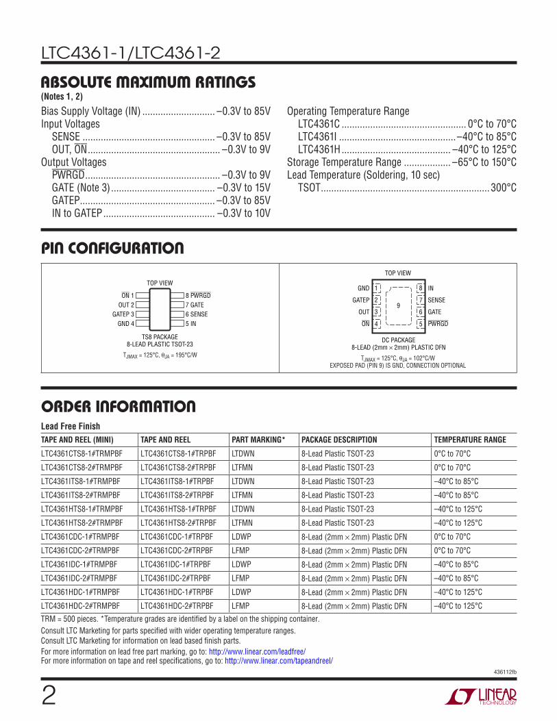
pin conFiguraTion
Operating Temperature Range LTC4361C ................................................ 0°C to 70°C LTC4361I .............................................–40°C to 85°C LTC4361H .......................................... –40°C to 125°C
Storage Temperature Range .................. –65°C to 150°CLead Temperature (Soldering, 10 sec) TSOT ................................................................. 300°C
ON 1OUT 2
GATEP 3GND 4
8 PWRGD7 GATE6 SENSE5 IN
TOP VIEW
TS8 PACKAGE8-LEAD PLASTIC TSOT-23
TJMAX = 125°C, θJA = 195°C/W
TOP VIEW
GND
GATEP
OUT
ON
IN
SENSE
GATE
PWRGD
DC PACKAGE8-LEAD (2mm × 2mm) PLASTIC DFN
9
4
1
2
3 6
5
7
8
TJMAX = 125°C, θJA = 102°C/W
EXPOSED PAD (PIN 9) IS GND, CONNECTION OPTIONAL
LTC4361-1/LTC4361-2
3436112fb
elecTrical characTerisTics The l denotes the specifications which apply over the full operating temperature range, otherwise specifications are at TA = 25°C. VIN = 5V, VON = 0V, unless otherwise noted.
SYMBOL PARAMETER CONDITIONS MIN TYP MAX UNITS
Supplies
VIN Input Voltage Range l 2.5 80 V
VIN(UVL) Input Undervoltage Lockout VIN Rising l 1.8 2.1 2.47 V
IIN Input Supply Current VON = 0V l 220 400 µA
VON = 2.5V l 1.5 10 µA
Thresholds
VIN(OV) IN Pin Overvoltage Threshold VIN Rising l 5.684 5.8 5.916 V
VIN(OVL) IN Pin Overvoltage Recovery Threshold VIN Falling l 5.51 5.7 5.85 V
∆VOV Overvoltage Hysteresis l 25 100 260 mV
∆VOC Overcurrent Threshold VIN – VSENSE l 45 50 55 mV
External Gate Drive
∆VGATE External N-Channel MOSFET Gate Drive (VGATE – VOUT)
2.5V ≤ VIN < 3V, IGATE = –1µA 3V ≤ VIN < 5.5V, IGATE = –1µA
l
l
3.5 4.5
4.5 6
6 7.9
V V
VGATE(TH) GATE High Threshold for PWRGD Status VIN = 3.3V VIN = 5V
l
l
5.7 6.7
6.3 7.2
6.8 7.8
V V
IGATE(UP) GATE Pull-Up Current VGATE = 1V l –4.5 –10 –15 µA
VGATE(UP) GATE Ramp-Up VGATE = 1V to 7V l 1.3 3 4.5 V/ms
IGATE(FST) GATE Pull-Down Current Fast Turn-Off, VIN = 6V, VGATE = 9V (C-, I-Grade) (H-Grade)
l
l
15 12
30 30
60 60
mA mA
IGATE(DN) GATE Pull-Down Current VON = 2.5V, VGATE = 9V l 5 40 80 µA
Input Pins
ISENSE(IN) SENSE Input Current VSENSE = 5V 10 nA
IOUT(IN) OUT Input Current VOUT = 5V, VON = 0V VOUT = 5V, VON = 2.5V
l
l
5 10 0
20 ±3
µA µA
VON(TH) ON Input Threshold l 0.4 1.5 V
ION ON Pull-Down Current VON = 2.5V l 2 5 10 µA
Output Pins
VGATEP(CLP) IN to GATEP Clamp Voltage VIN = 8V to 80V l 5 5.8 7.9 V
RGATEP GATEP Resistive Pull-Down VGATEP = 3V l 0.6 2 3.2 MΩ
VPWRGD(OL) PWRGD Output Low Voltage VIN = 5V, IPWRGD = 3mA (C-, I-Grade) (H-Grade)
l
l
0.23 0.23
0.4 0.5
V V
RPWRGD PWRGD Pull-Up Resistance to OUT VIN = 6.5V, VPWRGD = 1V l 220 500 800 kΩ
Delay
tON GATE On Delay VIN High to IGATE = –5µA l 50 130 219 ms
tOFF GATE Off Propagation Delay VIN = Step 5V to 6.5V to PWRGD High VIN – VSENSE = Step 0mV to 100mV
l
l
5
0.25 10
1 20
µs µs
tPWRGD PWRGD Delay VIN = Step 5V to 6.5V VGATE > VGATE(TH) to PWRGD Low
l
l
25
0.25 65
1 105
µs ms
tON(OFF) ON High to GATE Off VON = Step 0V to 2.5V l 2 5 µs
Note 1: Stresses beyond those listed under Absolute Maximum Ratings may cause permanent damage to the device. Exposure to any Absolute Maximum Rating condition for extended periods may affect device reliability and lifetime.
Note 2: All currents into device pins are positive; all currents out of device pins are negative. All voltages are referenced to GND unless otherwise specified.Note 3: An internal clamp limits VGATE to a minimum of 4.5V above VOUT. Driving this pin to voltages beyond this clamp may damage the device.
LTC4361-1/LTC4361-2
4436112fb
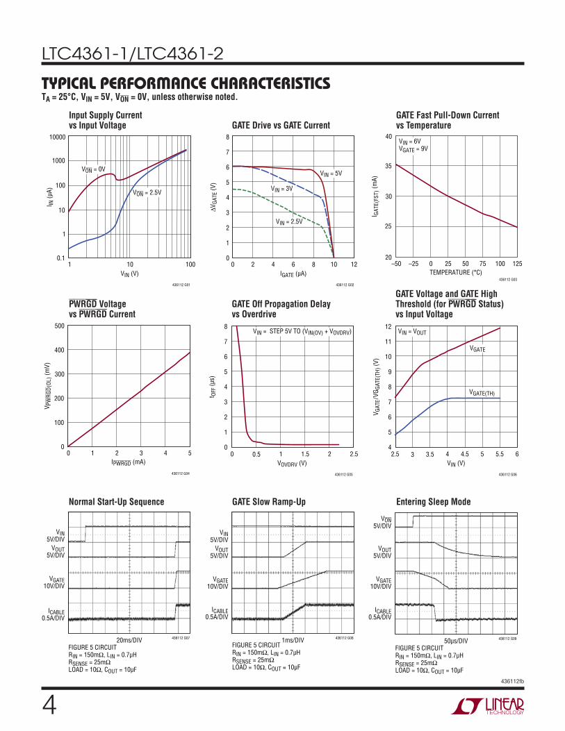
Typical perFormance characTerisTics
PWRGD Voltage vs PWRGD Current
GATE Off Propagation Delay vs Overdrive
Normal Start-Up Sequence GATE Slow Ramp-Up Entering Sleep Mode
Input Supply Current vs Input Voltage GATE Drive vs GATE Current
GATE Fast Pull-Down Current vs Temperature
VIN (V)1
0.1
I IN (µ
A)
1
100
1000
10000
100
436112 G01
10
10
VON = 0V
VON = 2.5V
IGATE (µA)0
0
∆VGA
TE (V
)
4
3
2
1
6
7
8
4 8 10 12
436112 G02
5
2 6
VIN = 5V
VIN = 3V
VIN = 2.5V
TEMPERATURE (°C)–50
20
I GAT
E(FS
T) (m
A)
25
30
35
40
–25 0 25
VIN = 6VVGATE = 9V
50
436112 G03
75 125100
IPWRGD (mA)0
0
V PWRGD
(OL)
(mV)
200
100
300
400
500
1 2 3 4
436112 G04
5VOVDRV (V)
00
t OFF
(µs)
2
1
4
0.5 1 1.5
436112 G05
2
6
8
3
5
7
2.5
VIN = STEP 5V TO (VIN(OV) + VOVDRV)
VIN5V/DIV
VGATE10V/DIV
VOUT5V/DIV
ICABLE0.5A/DIV
20ms/DIV 436112 G07
FIGURE 5 CIRCUITRIN = 150mΩ, LIN = 0.7µHRSENSE = 25mΩLOAD = 10Ω, COUT = 10µF
VIN5V/DIV
VGATE10V/DIV
VOUT5V/DIV
ICABLE0.5A/DIV
1ms/DIV 436112 G08
FIGURE 5 CIRCUITRIN = 150mΩ, LIN = 0.7µHRSENSE = 25mΩLOAD = 10Ω, COUT = 10µF
VON5V/DIV
VGATE10V/DIV
VOUT5V/DIV
ICABLE0.5A/DIV
50µs/DIV 436112 G09
FIGURE 5 CIRCUITRIN = 150mΩ, LIN = 0.7µHRSENSE = 25mΩLOAD = 10Ω, COUT = 10µF
TA = 25°C, VIN = 5V, VON = 0V, unless otherwise noted.
VIN (V)2.5
4
V GAT
E/VG
GATE
(TH)
(V)
6
5
8
3.5 43 54.5
436112 G06
5.5
10
12
7
9
11
6
VGATE
VGATE(TH)
VIN = VOUT
GATE Voltage and GATE High Threshold (for PWRGD Status) vs Input Voltage
LTC4361-1/LTC4361-2
5436112fb
pin FuncTionsExposed Pad (DFN): Ground. Connection to PCB is optional.
GATE: Gate Drive for External N-Channel MOSFET. An internal charge pump provides a 10µA pull-up current to charge the gate of the external N-channel MOSFET. An additional ramp circuit limits the GATE ramp rate when turning on to 3V/ms. For slower ramp rates, connect an external capacitor from GATE to GND. An internal clamp limits GATE to 6V above the OUT pin voltage. An internal GATE high comparator controls the PWRGD pin.
GATEP: Gate Drive for External P-Channel MOSFET. GATEP connects to the gate of an optional external P-channel MOS-FET to protect against negative voltages at IN. This pin is internally clamped to 5.8V below VIN. An internal 2M resis-tor connects this pin to ground. Connect to IN if not used.
GND: Device Ground.
IN: Supply Voltage Input. Connect this pin to the input power supply. This pin has an overvoltage threshold of 5.8V. After an overvoltage event, this pin must fall below
VIN(OV) – ∆VOV to release the overvoltage lockout. Dur-ing lockout, GATE is held low and the PWRGD pull-down releases.
ON: On Control Input. A logic low at ON enables the LTC4361. A logic high at ON activates a low current pull-down at the GATE pin and causes the LTC4361 to enter a low current sleep mode. An internal 5µA current pulls ON down to ground. Connect to ground or leave open if unused.
OUT: Output Voltage Sense Input for GATE Clamp. Connect to the source of the external N-channel MOSFET to sense the output voltage for GATE to OUT clamp.
PWRGD: Power Good Status. Open-drain output with internal 500k resistive pull-up to OUT. Pulls low 65ms after GATE ramps above VGATE(TH).
SENSE: Current Sense Input. Connect a sense resistor between IN and SENSE. An overcurrent protection circuit turns off the N-channel MOSFET when the voltage across the sense resistor exceeds 50mV for more than 10µs.
LTC4361-1/LTC4361-2
6436112fb
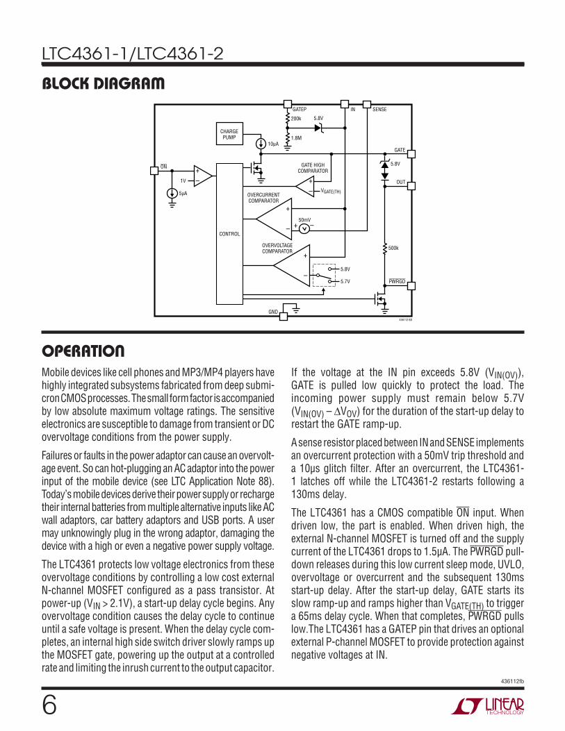
operaTionMobile devices like cell phones and MP3/MP4 players have highly integrated subsystems fabricated from deep submi-cron CMOS processes. The small form factor is accompanied by low absolute maximum voltage ratings. The sensitive electronics are susceptible to damage from transient or DC overvoltage conditions from the power supply.
Failures or faults in the power adaptor can cause an overvolt-age event. So can hot-plugging an AC adaptor into the power input of the mobile device (see LTC Application Note 88). Today’s mobile devices derive their power supply or recharge their internal batteries from multiple alternative inputs like AC wall adaptors, car battery adaptors and USB ports. A user may unknowingly plug in the wrong adaptor, damaging the device with a high or even a negative power supply voltage.
The LTC4361 protects low voltage electronics from these overvoltage conditions by controlling a low cost external N-channel MOSFET configured as a pass transistor. At power-up (VIN > 2.1V), a start-up delay cycle begins. Any overvoltage condition causes the delay cycle to continue until a safe voltage is present. When the delay cycle com-pletes, an internal high side switch driver slowly ramps up the MOSFET gate, powering up the output at a controlled rate and limiting the inrush current to the output capacitor.
If the voltage at the IN pin exceeds 5.8V (VIN(OV)), GATE is pulled low quickly to protect the load. The incoming power supply must remain below 5.7V (VIN(OV) – ∆VOV) for the duration of the start-up delay to restart the GATE ramp-up.
A sense resistor placed between IN and SENSE implements an overcurrent protection with a 50mV trip threshold and a 10µs glitch filter. After an overcurrent, the LTC4361-1 latches off while the LTC4361-2 restarts following a 130ms delay.
The LTC4361 has a CMOS compatible ON input. When driven low, the part is enabled. When driven high, the external N-channel MOSFET is turned off and the supply current of the LTC4361 drops to 1.5µA. The PWRGD pull-down releases during this low current sleep mode, UVLO, overvoltage or overcurrent and the subsequent 130ms start-up delay. After the start-up delay, GATE starts its slow ramp-up and ramps higher than VGATE(TH) to trigger a 65ms delay cycle. When that completes, PWRGD pulls low.The LTC4361 has a GATEP pin that drives an optional external P-channel MOSFET to provide protection against negative voltages at IN.
block Diagram
–
+
GND436112 BD
10µA
ON
OUT
PWRGD
5.8V
500k
GATE
CONTROL
CHARGEPUMP
OVERCURRENTCOMPARATOR
50mV+ –
–
+
5.8V
5.7V
OVERVOLTAGECOMPARATOR
IN SENSE
1.8M
200k 5.8V
GATEP
5µA
1V
+–
VGATE(TH)
GATE HIGHCOMPARATOR
+–
LTC4361-1/LTC4361-2
7436112fb
The typical LTC4361 application protects 2.5V to 5.5V systems in portable devices from power supply overvolt-age. The basic application circuit is shown in Figure 1. Device operation and external component selection is discussed in detail in the following sections.
applicaTions inFormaTion
Figure 1. Protection from Input Overvoltage and Overcurrent
GATE
M1Si1470DH
RSENSE0.025Ω
SENSE
IN
436112 F01
VOUT5V1.5A
VIN5V
LTC4361
OUT
PWRGDONGND
COUT10µF
The GATE ramp rate is limited to 3V/ms. VOUT follows at a similar rate which results in an inrush current into the load capacitor COUT of:
IINRUSH = COUT •
dVGATEdt
= COUT • 3 mA/µF[ ]
The servo loop is compensated by the parasitic capaci-tance of the external MOSFET. No further compensation components are normally required. In the case where the parasitic capacitance is less than 100pF, a 100pF compensation capacitor between GATE and ground may be required.
An even slower GATE ramp and lower inrush current can be achieved by connecting an external capacitor, CG, from GATE to ground. The voltage at GATE then ramps up with a slope equal to 10µA/CG [V/s]. Choose CG using the formula:
CG = 10µA
IINRUSH•COUT
Overvoltage
When power is first applied, VIN must remain below 5.7V (VIN(OV) – ∆VOV) for more than 130ms before GATE is ramped up to turn on the MOSFET. If VIN then rises above 5.8V (VIN(OV)), the overvoltage comparator activates the 30mA fast pull-down on GATE within 1µs. After an over-voltage condition, the MOSFET is held off until VIN once again remains below 5.7V for 130ms.
Overcurrent
The overcurrent comparator protects the MOSFET from excessive current. It trips when the SENSE pin falls more than 50mV below IN for 10µs. When the overcurrent comparator trips, GATE is pulled low quickly and the PWRGD pull-down releases. The LTC4361-2 automatically tries to apply power again after a 130ms start-up delay.
Start-Up
When VIN is less than the undervoltage lockout level of 2.1V, the GATE driver is held low and the PWRGD pull-down is high impedance. When VIN rises above 2.1V and ON is held low, a 130ms delay cycle starts. Any undervoltage or overvoltage event at IN (VIN < 2.1V or VIN > 5.7V) restarts the delay cycle. This delay allows the N-channel MOSFET to isolate the output from any input transients that occur at start-up. When the delay cycle completes, GATE starts its slow ramp-up.
GATE Control
An internal charge pump provides a gate overdrive greater than 3.5V when 2.5V ≤ VIN < 3V. If VIN ≥ 3V, the gate drive is guaranteed to be greater than 4.5V. This allows the use of logic-level N-channel MOSFETs. An internal 6V clamp between GATE and OUT protects the MOSFET gate.
LTC4361-1/LTC4361-2
8436112fb
applicaTions inFormaTionThe LTC4361-1 has an internal latch that maintains this off state until it is reset. To reset this latch, cycle IN be-low 2.1V (VIN(UVL)) or ON above 1.5V (VON(TH)) for more than 500µs. After reset, the LTC4361-1 goes through the start-up cycle.
In applications not requiring the overcurrent protection, tie the SENSE pin to the IN pin. To implement an overcurrent threshold ITRIP , choose RSENSE using the formula:
RSENSE =
∆VOCITRIP
After choosing the RSENSE, keep in mind that:
ITRIP(MAX) =∆VOC(MAX)
RSENSE(MIN)
ITRIP(MIN) =∆VOC(MIN)
RSENSE(MAX)
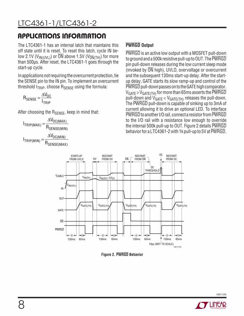
PWRGD Output
PWRGD is an active low output with a MOSFET pull-down to ground and a 500k resistive pull-up to OUT. The PWRGD pin pull-down releases during the low current sleep mode (invoked by ON high), UVLO, overvoltage or overcurrent and the subsequent 130ms start-up delay. After the start-up delay, GATE starts its slow ramp-up and control of the PWRGD pull-down passes on to the GATE high comparator. VGATE > VGATE(TH) for more than 65ms asserts the PWRGD pull-down and VGATE < VGATE(TH) releases the pull-down. The PWRGD pull-down is capable of sinking up to 3mA of current allowing it to drive an optional LED. To interface PWRGD to another I/O rail, connect a resistor from PWRGD to the I/O rail with a resistance low enough to override the internal 500k pull-up to OUT. Figure 2 details PWRGD behavior for a LTC4361-2 with 1k pull-up to 5V at PWRGD.
IN
OUT
GATE
ON
PWRGD
VGATE(TH)VGATE(TH)VGATE(TH)VGATE(TH)VGATE(TH)
VIN(UVL)
ICABLE
OCTHRESHOLD
10µs (NOT TO SCALE)436112 F02
VIN(OV)–∆VOV
START-UPFROM UVLO
RESTARTFROM OVOV
RESTARTFROM ONON
RESTARTFROM OC
OC
VIN(OV)
130ms 65ms 130ms 65ms 130ms 65ms 130ms 65ms
Figure 2. PWRGD Behavior
LTC4361-1/LTC4361-2
9436112fb
applicaTions inFormaTionON Input
ON is a CMOS compatible, active low enable input. It has a default 5µA pull-down to ground. Connect this pin to ground or leave open to enable normal device operation. If it is driven high while the external MOSFET is turned on, GATE is pulled low with a weak pull-down current (40µA) to turn off the external MOSFET gradually, minimizing input voltage transients. The LTC4361 then goes into a low current sleep mode, drawing only 1.5µA at IN. When ON goes back low, the part restarts with a 130ms delay cycle.
GATEP Control
GATEP has a 2M resistive pull-down to ground and a 5.8V Zener clamp in series with a 200k resistor to IN. It con-trols the gate of an optional external P-channel MOSFET to provide negative voltage protection. The 2M resistive pull-down turns on the MOSFET once VIN – VGATEP is more than the MOSFET gate threshold voltage. The IN to GATEP Zener protects the MOSFET from gate overvoltage by clamping its VGS to 5.8V when VIN goes high.
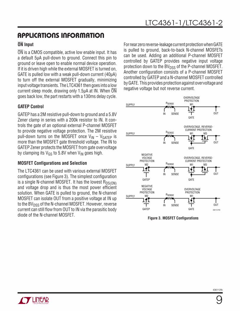
MOSFET Configurations and Selection
The LTC4361 can be used with various external MOSFET configurations (see Figure 3). The simplest configuration is a single N-channel MOSFET. It has the lowest RDS(ON) and voltage drop and is thus the most power efficient solution. When GATE is pulled to ground, the N-channel MOSFET can isolate OUT from a positive voltage at IN up to the BVDSS of the N-channel MOSFET. However, reverse current can still flow from OUT to IN via the parasitic body diode of the N-channel MOSFET.
For near zero reverse-leakage current protection when GATE is pulled to ground, back-to-back N-channel MOSFETs can be used. Adding an additional P-channel MOSFET controlled by GATEP provides negative input voltage protection down to the BVDSS of the P-channel MOSFET. Another configuration consists of a P-channel MOSFET controlled by GATEP and a N-channel MOSFET controlled by GATE. This provides protection against overvoltage and negative voltage but not reverse current.
Figure 3. MOSFET Configurations
GATEP
OVERVOLTAGE, REVERSE-CURRENT PROTECTION
NEGATIVEVOLTAGE
PROTECTION
GATE
OVERVOLTAGE, REVERSE-CURRENT PROTECTION
GATE
GATE
GATEP
SUPPLY
SUPPLY
SUPPLY
SUPPLY
436112 F03
OVERVOLTAGEPROTECTION
OVERVOLTAGEPROTECTION
M1
M1 M3
M1M2
M1M2
M3
NEGATIVEVOLTAGE
PROTECTION
GATEOUT
OUT
OUT
IN
RSENSE
SENSE OUT
IN
RSENSE
SENSE
IN
RSENSE
SENSE
IN
RSENSE
SENSE
LTC4361-1/LTC4361-2
10436112fb
applicaTions inFormaTion
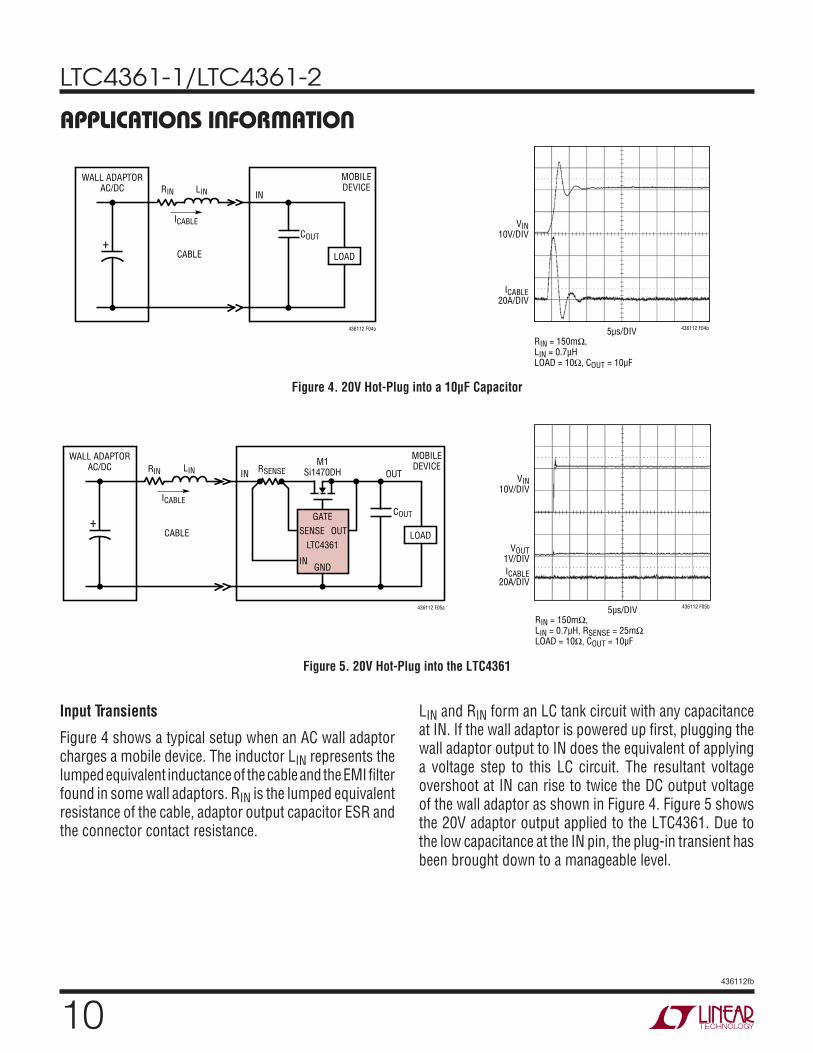
Figure 4. 20V Hot-Plug into a 10µF Capacitor
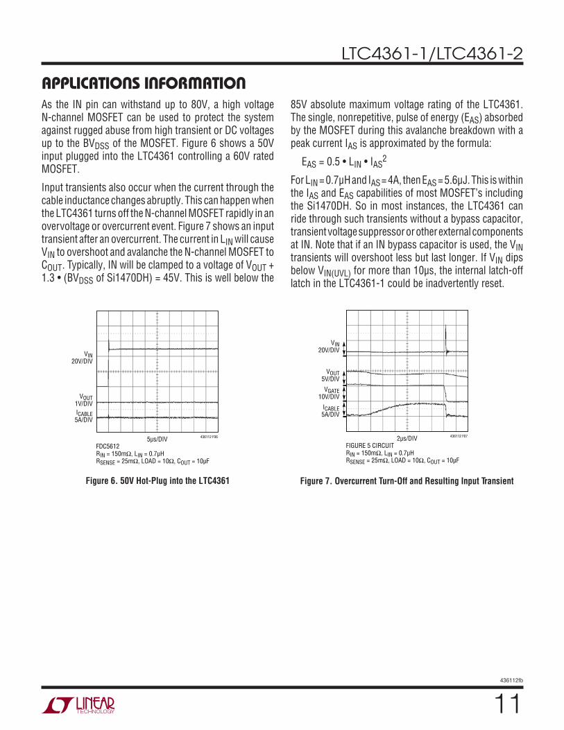
Figure 5. 20V Hot-Plug into the LTC4361
+LOAD
436112 F04a
MOBILEDEVICE
WALL ADAPTORAC/DC
COUT
INLINRIN
CABLE
ICABLE VIN10V/DIV
ICABLE20A/DIV
5µs/DIV 436112 F04b
RIN = 150mΩ, LIN = 0.7µHLOAD = 10Ω, COUT = 10µF
+LOAD
LTC4361
M1Si1470DH
GATE
GND
436112 F05a
MOBILEDEVICE
WALL ADAPTORAC/DC
COUT
SENSE OUT
IN
IN OUTLINRIN RSENSE
CABLE
ICABLE
VIN10V/DIV
VOUT1V/DIVICABLE
20A/DIV
5µs/DIV 436112 F05b
RIN = 150mΩ, LIN = 0.7µH, RSENSE = 25mΩLOAD = 10Ω, COUT = 10µF
Input Transients
Figure 4 shows a typical setup when an AC wall adaptor charges a mobile device. The inductor LIN represents the lumped equivalent inductance of the cable and the EMI filter found in some wall adaptors. RIN is the lumped equivalent resistance of the cable, adaptor output capacitor ESR and the connector contact resistance.
LIN and RIN form an LC tank circuit with any capacitance at IN. If the wall adaptor is powered up first, plugging the wall adaptor output to IN does the equivalent of applying a voltage step to this LC circuit. The resultant voltage overshoot at IN can rise to twice the DC output voltage of the wall adaptor as shown in Figure 4. Figure 5 shows the 20V adaptor output applied to the LTC4361. Due to the low capacitance at the IN pin, the plug-in transient has been brought down to a manageable level.
LTC4361-1/LTC4361-2
11436112fb
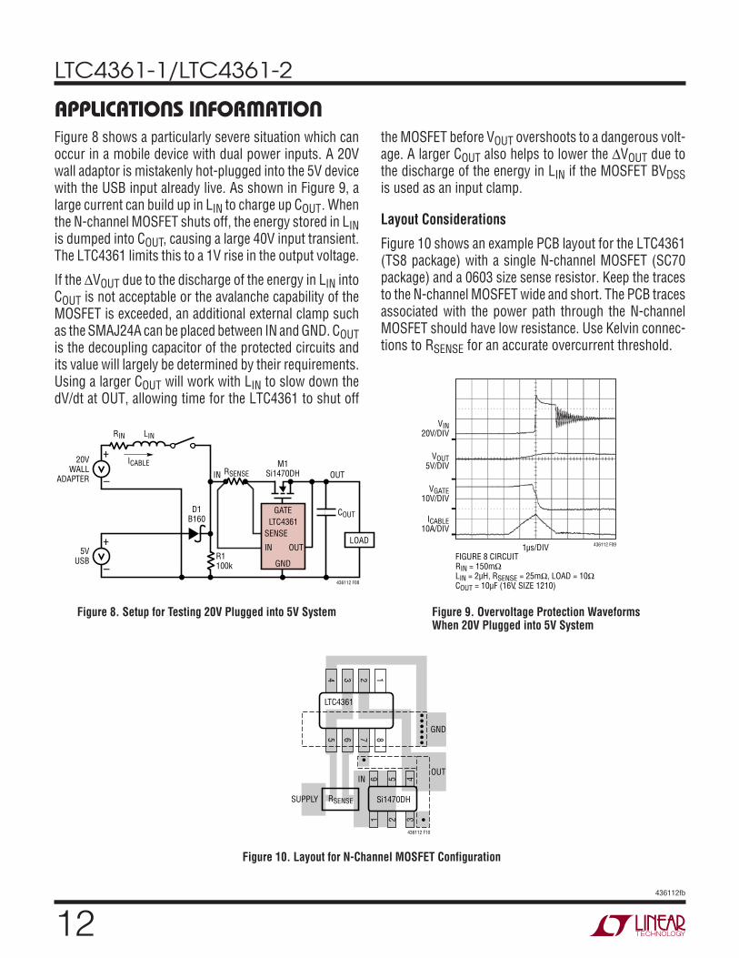
applicaTions inFormaTionAs the IN pin can withstand up to 80V, a high voltage N-channel MOSFET can be used to protect the system against rugged abuse from high transient or DC voltages up to the BVDSS of the MOSFET. Figure 6 shows a 50V input plugged into the LTC4361 controlling a 60V rated MOSFET.
Input transients also occur when the current through the cable inductance changes abruptly. This can happen when the LTC4361 turns off the N-channel MOSFET rapidly in an overvoltage or overcurrent event. Figure 7 shows an input transient after an overcurrent. The current in LIN will cause VIN to overshoot and avalanche the N-channel MOSFET to COUT . Typically, IN will be clamped to a voltage of VOUT + 1.3 • (BVDSS of Si1470DH) = 45V. This is well below the
85V absolute maximum voltage rating of the LTC4361. The single, nonrepetitive, pulse of energy (EAS) absorbed by the MOSFET during this avalanche breakdown with a peak current IAS is approximated by the formula:
EAS = 0.5 • LIN • IAS2
For LIN = 0.7μH and IAS = 4A, then EAS = 5.6μJ. This is within the IAS and EAS capabilities of most MOSFET’s including the Si1470DH. So in most instances, the LTC4361 can ride through such transients without a bypass capacitor, transient voltage suppressor or other external components at IN. Note that if an IN bypass capacitor is used, the VIN transients will overshoot less but last longer. If VIN dips below VIN(UVL) for more than 10µs, the internal latch-off latch in the LTC4361-1 could be inadvertently reset.
Figure 6. 50V Hot-Plug into the LTC4361 Figure 7. Overcurrent Turn-Off and Resulting Input Transient
VIN20V/DIV
VOUT1V/DIVICABLE5A/DIV
5µs/DIV 436112 F06
FDC5612RIN = 150mΩ, LIN = 0.7µHRSENSE = 25mΩ, LOAD = 10Ω, COUT = 10µF
VIN20V/DIV
VGATE10V/DIV
VOUT5V/DIV
ICABLE5A/DIV
2µs/DIV 436112 F07
FIGURE 5 CIRCUITRIN = 150mΩ, LIN = 0.7µHRSENSE = 25mΩ, LOAD = 10Ω, COUT = 10µF
LTC4361-1/LTC4361-2
12436112fb
Figure 10. Layout for N-Channel MOSFET Configuration
Figure 8. Setup for Testing 20V Plugged into 5V System Figure 9. Overvoltage Protection Waveforms When 20V Plugged into 5V System
LOAD
436112 F08
OUTM1
Si1470DH
COUT
IN RSENSE
LIN
D1B160
RIN
20VWALL
ADAPTER
5VUSB R1
100k
LTC4361
GND
GATE
+
–
+
–
ICABLE
SENSE
IN OUT
VIN20V/DIV
VGATE10V/DIV
VOUT5V/DIV
ICABLE10A/DIV
1µs/DIV 436112 F09
FIGURE 8 CIRCUITRIN = 150mΩLIN = 2µH, RSENSE = 25mΩ, LOAD = 10ΩCOUT = 10µF (16V, SIZE 1210)
LTC4361
436112 F10
865
1
7234
Si1470DH
OUTIN
SUPPLY
GND
RSENSE
1 2 3
6 5 4
Figure 8 shows a particularly severe situation which can occur in a mobile device with dual power inputs. A 20V wall adaptor is mistakenly hot-plugged into the 5V device with the USB input already live. As shown in Figure 9, a large current can build up in LIN to charge up COUT . When the N-channel MOSFET shuts off, the energy stored in LIN is dumped into COUT, causing a large 40V input transient. The LTC4361 limits this to a 1V rise in the output voltage.
If the ∆VOUT due to the discharge of the energy in LIN into COUT is not acceptable or the avalanche capability of the MOSFET is exceeded, an additional external clamp such as the SMAJ24A can be placed between IN and GND. COUT is the decoupling capacitor of the protected circuits and its value will largely be determined by their requirements. Using a larger COUT will work with LIN to slow down the dV/dt at OUT, allowing time for the LTC4361 to shut off
the MOSFET before VOUT overshoots to a dangerous volt-age. A larger COUT also helps to lower the ∆VOUT due to the discharge of the energy in LIN if the MOSFET BVDSS is used as an input clamp.
Layout Considerations
Figure 10 shows an example PCB layout for the LTC4361 (TS8 package) with a single N-channel MOSFET (SC70 package) and a 0603 size sense resistor. Keep the traces to the N-channel MOSFET wide and short. The PCB traces associated with the power path through the N-channel MOSFET should have low resistance. Use Kelvin connec-tions to RSENSE for an accurate overcurrent threshold.
applicaTions inFormaTion
LTC4361-1/LTC4361-2
13436112fb
2.00 ±0.10(4 SIDES)
NOTE:1. DRAWING IS NOT A JEDEC PACKAGE OUTLINE2. DRAWING NOT TO SCALE3. ALL DIMENSIONS ARE IN MILLIMETERS4. DIMENSIONS OF EXPOSED PAD ON BOTTOM OF PACKAGE DO NOT INCLUDE MOLD FLASH. MOLD FLASH, IF PRESENT, SHALL NOT EXCEED 0.15mm ON ANY SIDE5. EXPOSED PAD SHALL BE SOLDER PLATED 6. SHADED AREA IS ONLY A REFERENCE FOR PIN 1 LOCATION ON THE TOP AND BOTTOM OF PACKAGE
0.40 ±0.10
BOTTOM VIEW—EXPOSED PAD
0.64 ±0.10(2 SIDES)
0.75 ±0.05
R = 0.115TYP
R = 0.05TYP
1.37 ±0.10(2 SIDES)
14
85
PIN 1 BARTOP MARK
(SEE NOTE 6)
0.200 REF
0.00 – 0.05
(DC8) DFN 0409 REVA
0.23 ±0.050.45 BSC
0.25 ±0.05
1.37 ±0.05(2 SIDES)
RECOMMENDED SOLDER PAD PITCH AND DIMENSIONSAPPLY SOLDER MASK TO AREAS THAT ARE NOT SOLDERED
0.64 ±0.05(2 SIDES)
1.15 ±0.05
0.70 ±0.05
2.55 ±0.05
PACKAGEOUTLINE
0.45 BSC
PIN 1 NOTCH R = 0.20 OR 0.25 × 45° CHAMFER
DC8 Package8-Lead Plastic DFN (2mm × 2mm)
(Reference LTC DWG # 05-08-1719 Rev A)
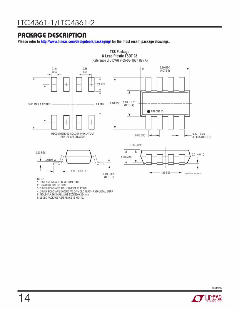
package DescripTionPlease refer to http://www.linear.com/designtools/packaging/ for the most recent package drawings.
LTC4361-1/LTC4361-2
14436112fb
1.50 – 1.75(NOTE 4)
2.80 BSC
0.22 – 0.36 8 PLCS (NOTE 3)
DATUM ‘A’
0.09 – 0.20(NOTE 3)
TS8 TSOT-23 0710 REV A
2.90 BSC(NOTE 4)
0.65 BSC
1.95 BSC
0.80 – 0.90
1.00 MAX0.01 – 0.10
0.20 BSC
0.30 – 0.50 REF
PIN ONE ID
NOTE:1. DIMENSIONS ARE IN MILLIMETERS2. DRAWING NOT TO SCALE3. DIMENSIONS ARE INCLUSIVE OF PLATING4. DIMENSIONS ARE EXCLUSIVE OF MOLD FLASH AND METAL BURR5. MOLD FLASH SHALL NOT EXCEED 0.254mm6. JEDEC PACKAGE REFERENCE IS MO-193
3.85 MAX
0.40MAX
0.65REF
RECOMMENDED SOLDER PAD LAYOUTPER IPC CALCULATOR
1.4 MIN2.62 REF
1.22 REF
TS8 Package8-Lead Plastic TSOT-23
(Reference LTC DWG # 05-08-1637 Rev A)
package DescripTionPlease refer to http://www.linear.com/designtools/packaging/ for the most recent package drawings.
LTC4361-1/LTC4361-2
15436112fb
Information furnished by Linear Technology Corporation is believed to be accurate and reliable. However, no responsibility is assumed for its use. Linear Technology Corporation makes no representa-tion that the interconnection of its circuits as described herein will not infringe on existing patent rights.
revision hisToryREV DATE DESCRIPTION PAGE NUMBER
A 01/11 Revised conditions for VGATE(CLP) and tOFF in Electrical Characteristics sectionRevised GATE Control in Applications Information section
37
B 05/12 Added H-grade order informationChange to Electrical Characteristics Input Undervoltage LockoutAdded VIN(OVL) specificationsChange to Electrical Characteristics Overvoltage HysteresisChange to Electrical Characteristics GATE Pull-Up and Pull-Down CurrentChange to Electrical Characteristics GATE Ramp-UpAdded ISENSE(IN) specificationsChange to Electrical Characteristics ON Pull-Down CurrentChange to Electrical Characteristics IN to GATEP Clamp VoltageChange to Electrical Characteristics GATEP Resistive Pull-DownChange to Electrical Characteristics PWRGD Pull-Up Resistance to OUTChange to Electrical Characteristics GATE On DelayChange to Electrical Characteristics PWRGD DelayReplaced GATE Fast Pull-Down Current vs Temperature CurveAdded PCB trace to short pin 3 to pin 5 in Figure 10Added packaging link
23333333333334
1213, 14
LTC4361-1/LTC4361-2
16436112fb
Linear Technology Corporation1630 McCarthy Blvd., Milpitas, CA 95035-7417 (408) 432-1900 FAX: (408) 434-0507 www.linear.com LINEAR TECHNOLOGY CORPORATION 2010
LT 0512 REV B • PRINTED IN USA
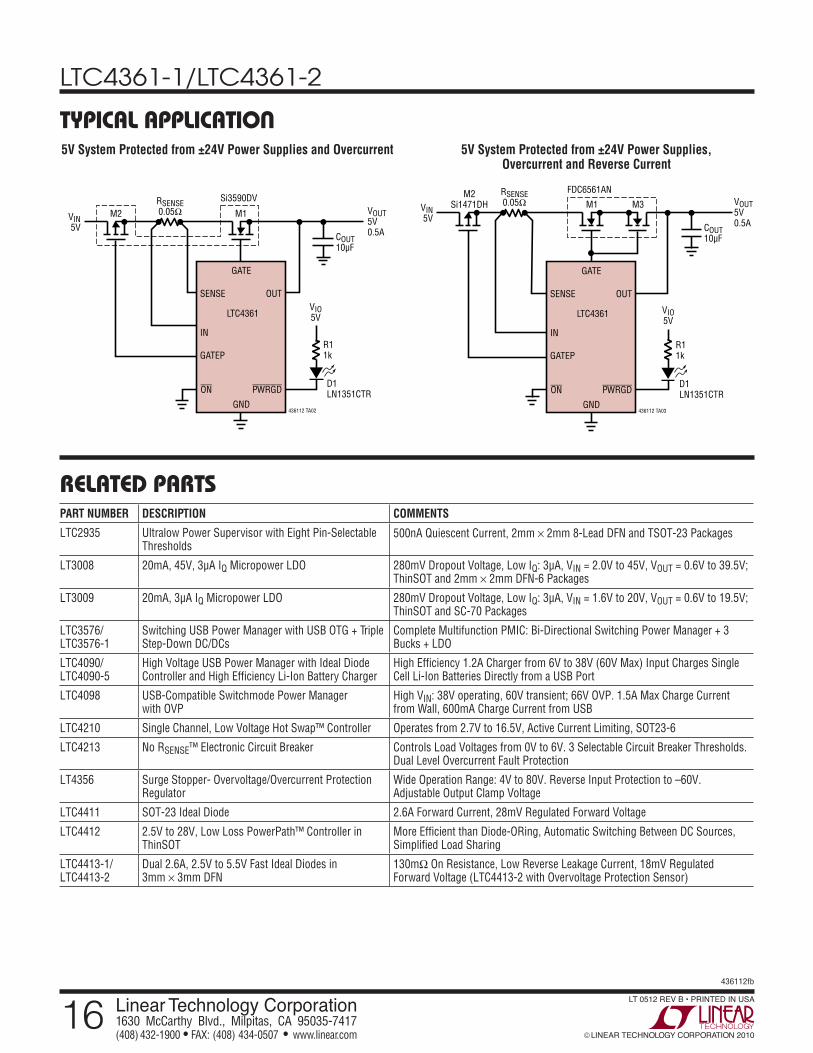
Typical applicaTion5V System Protected from ±24V Power Supplies,
Overcurrent and Reverse Current
relaTeD parTsPART NUMBER DESCRIPTION COMMENTS
LTC2935 Ultralow Power Supervisor with Eight Pin-Selectable Thresholds
500nA Quiescent Current, 2mm × 2mm 8-Lead DFN and TSOT-23 Packages
LT3008 20mA, 45V, 3µA IQ Micropower LDO 280mV Dropout Voltage, Low IQ: 3µA, VIN = 2.0V to 45V, VOUT = 0.6V to 39.5V; ThinSOT and 2mm × 2mm DFN-6 Packages
LT3009 20mA, 3µA IQ Micropower LDO 280mV Dropout Voltage, Low IQ: 3µA, VIN = 1.6V to 20V, VOUT = 0.6V to 19.5V; ThinSOT and SC-70 Packages
LTC3576/LTC3576-1
Switching USB Power Manager with USB OTG + Triple Step-Down DC/DCs
Complete Multifunction PMIC: Bi-Directional Switching Power Manager + 3 Bucks + LDO
LTC4090/LTC4090-5
High Voltage USB Power Manager with Ideal Diode Controller and High Efficiency Li-Ion Battery Charger
High Efficiency 1.2A Charger from 6V to 38V (60V Max) Input Charges Single Cell Li-Ion Batteries Directly from a USB Port
LTC4098 USB-Compatible Switchmode Power Manager with OVP
High VIN: 38V operating, 60V transient; 66V OVP. 1.5A Max Charge Current from Wall, 600mA Charge Current from USB
LTC4210 Single Channel, Low Voltage Hot Swap™ Controller Operates from 2.7V to 16.5V, Active Current Limiting, SOT23-6
LTC4213 No RSENSE™ Electronic Circuit Breaker Controls Load Voltages from 0V to 6V. 3 Selectable Circuit Breaker Thresholds. Dual Level Overcurrent Fault Protection
LT4356 Surge Stopper- Overvoltage/Overcurrent Protection Regulator
Wide Operation Range: 4V to 80V. Reverse Input Protection to –60V. Adjustable Output Clamp Voltage
LTC4411 SOT-23 Ideal Diode 2.6A Forward Current, 28mV Regulated Forward Voltage
LTC4412 2.5V to 28V, Low Loss PowerPath™ Controller in ThinSOT
More Efficient than Diode-ORing, Automatic Switching Between DC Sources, Simplified Load Sharing
LTC4413-1/LTC4413-2
Dual 2.6A, 2.5V to 5.5V Fast Ideal Diodes in 3mm × 3mm DFN
130mΩ On Resistance, Low Reverse Leakage Current, 18mV Regulated Forward Voltage (LTC4413-2 with Overvoltage Protection Sensor)
5V System Protected from ±24V Power Supplies and Overcurrent
Si3590DVRSENSE0.05Ω
436112 TA02
VOUT5V0.5ACOUT
10µF
M2 M1
D1LN1351CTR
R11k
VIO5V
VIN5V
GATE
SENSE
IN
LTC4361
GATEP
OUT
PWRGDON
GND
M2Si1471DH
FDC6561ANRSENSE0.05Ω
436112 TA03
VOUT5V0.5ACOUT
10µF
M1 M3
D1LN1351CTR
R11k
VIO5V
VIN5V
GATE
SENSE
IN
LTC4361
GATEP
OUT
PWRGDON
GND