Embed Size (px)
Citation preview
LTC4282
1Rev. A
For more information www.analog.comDocument Feedback
All registered trademarks and trademarks are the property of their respective owners. Patents pending.
TYPICAL APPLICATION
FEATURES DESCRIPTION
High Current Hot Swap Controller with I2C Compatible Monitoring
The LTC®4282 hot swap controller allows a board to be safely inserted and removed from a live backplane. Using one or more external N-channel pass transistors, board supply voltage and inrush current are ramped up at an adjustable rate. An I2C interface and onboard ADC allows for monitoring of board current, voltage, power, energy and fault status.
The device features analog foldback current limiting and supply monitoring for applications from 2.9V to 33V. Dual 12V gate drive allows high power applications to either share safe operating area across parallel MOSFETs or support a 2-stage start-up that first charges the load capacitance followed by enabling a low on-resistance path to the load.
The LTC4282 is well suited to high power applications because the precise monitoring capability and accurate current limiting reduce the extremes in which both loads and power supplies must safely operate. Non-volatile con-figuration allows for flexibility in the autonomous genera-tion of alerts and response to faults.
12V, 100A Plug-In Board Application Start-Up Waveforms
APPLICATIONS
n Allows Safe Board Insertion Into Live Backplane n 12-/16-Bit ADC with ±0.7% Total Unadjusted Error n Monitors Current, Voltage, Power and Energy n Controls Two Parallel N-Channel MOSFETs for SOA
Sharing in High Current Applications n Internal EEPROM for Nonvolatile Configuration n Wide Operating Voltage Range: 2.9V to 33V n I2C/SMBus Digital Interface (Coexists with PMBus
Devices) n 12V Gate Drive for Lower MOSFET RDS(ON) n Programmable Current Limit with 2% Accuracy n MOSFET Power Limiting with Current Foldback n Continuously Monitors MOSFET Health n Stores Minimum and Maximum Measurements n Alerts When Alarm Thresholds Exceeded n Input Overvoltage and Undervoltage Protection n Three General Purpose Input/Outputs n Internal ±5% or External Timebases n 32-Pin 5mm × 5mm QFN Package
n Enterprise Servers and Data Storage Systems n Network Routers and Switches n Base Stations n Platform Management
+
VDD
SMCJ15CA×2
GATE1 GATE2
10nF
TIMER
LTC4282
INTVCC
CONN
ECTO
R 1
CONN
ECTO
R 2
PLUG-INBOARD
NC
100k
NCNC
NC
4282 TA01
GND
12V
SDASCL
ALERT
10Ω
10Ω
VOUT12V100A
0.25mΩ
0.25mΩ
SOURCE
FB
GPIO1 POWERGOOD
UVOVSDAISDAOSCLALERTADR0ADR1ADR2ON
SENSE2+ SENSE1+ SENSE1– SENSE2–ADC+
1Ω1Ω 1Ω1Ω
ADC–
WP GNDCLKOUT
NC
CLKIN
4.7µF
12V
BACKPLANE
GPIO2
GPIO3
GP
GP20ms/DIV
∆VGATE10V/DIV
GPIO1(PG)10V/DIV
VDD10V/DIV
VSOURCE10V/DIV
50ms DE-BOUNCE
4282 TA01b
CONTACT BOUNCE
LTC4282
2Rev. A
For more information www.analog.com
Features ..................................................... 1Applications ................................................ 1Typical Application ........................................ 1Description.................................................. 1Absolute Maximum Ratings .............................. 3Order Information .......................................... 3Electrical Characteristics ................................. 3Pin Configuration .......................................... 3Electrical Characteristics ................................. 4Timing Diagram ............................................ 6Typical Performance Characteristics ................... 7Pin Functions ............................................... 9Functional Diagram ...................................... 11Operation................................................... 12Applications Information ................................ 13
Turn-On Sequence ................................................. 13Turn-Off Sequence .................................................. 14Current Limit Adjustment ........................................ 15Constant Current Start-Up Using GATE R-C Networks ................................................................ 15Current Limit Stability ............................................. 15Parasitic MOSFET Oscillations ................................ 15Overcurrent Fault .................................................... 16Advantages of Dual Gate Drivers ............................ 16Overvoltage Fault .................................................... 17Undervoltage Fault ..................................................20ON/OFF Control .......................................................20
FET Bad Fault .......................................................... 21FET Short Fault .......................................................22Power Bad Fault ......................................................22Fault Alerts .............................................................22Resetting Faults in FAULT_LOG ..............................23Reboot ....................................................................23Data Converters ......................................................23Crystal Oscillator/External Clock .............................25Configuring the GPIO Pins ......................................25Supply Transients ...................................................26Design Example ......................................................26Layout Considerations ............................................28Digital Interface ......................................................29START and STOP Conditions ..................................29I2C Device Addressing ............................................29Acknowledge ..........................................................29Write Protocol.........................................................29Read Protocol .........................................................29Data Synchronization .............................................. 31Alert Response Protocol ......................................... 31EEPROM ................................................................. 31
Register Set ............................................... 33Detailed I2C Command Register Descriptions ....... 34Typical Applications ...................................... 46Package Description ..................................... 48Revision History .......................................... 49Typical Application ....................................... 50Related Parts .............................................. 50
TABLE OF CONTENTS
LTC4282
3Rev. A
For more information www.analog.com
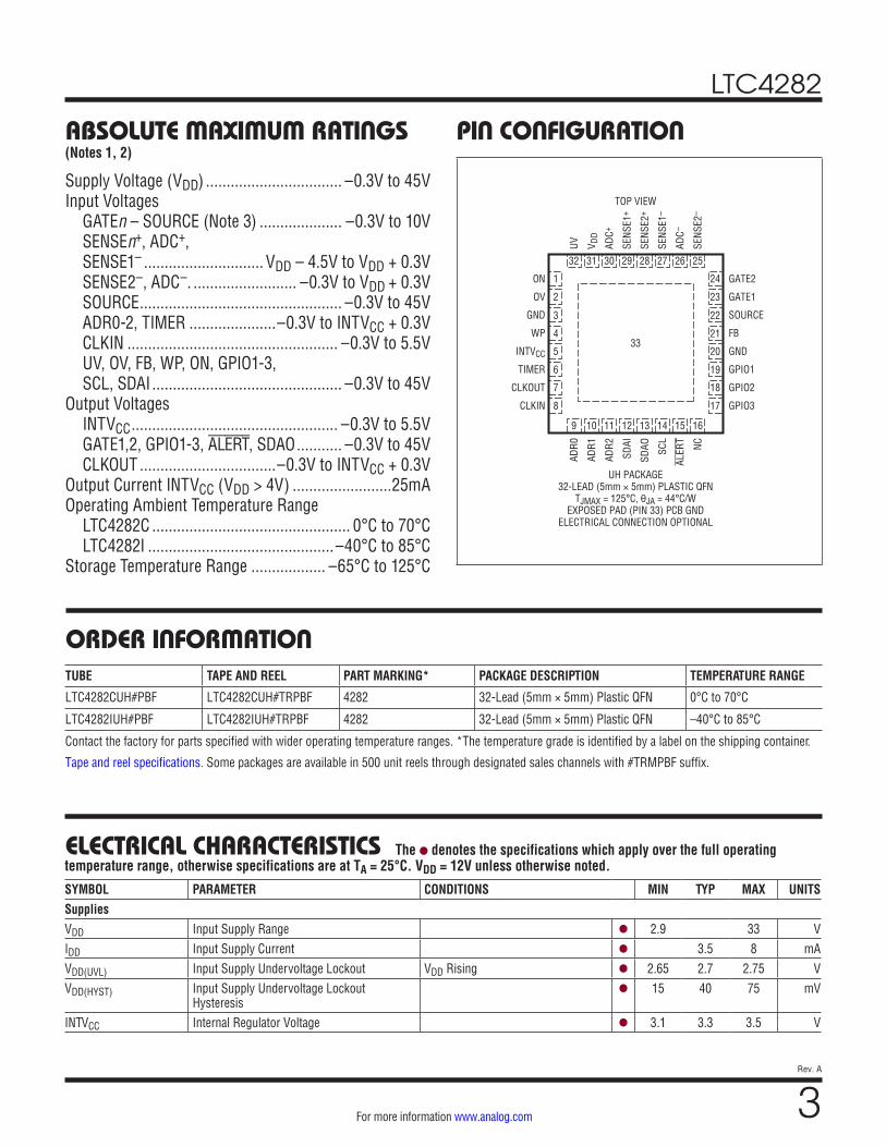
PIN CONFIGURATIONABSOLUTE MAXIMUM RATINGS
Supply Voltage (VDD) ................................. –0.3V to 45VInput Voltages GATEn – SOURCE (Note 3) .................... –0.3V to 10V SENSEn+, ADC+, SENSE1– ............................. VDD – 4.5V to VDD + 0.3V SENSE2–, ADC–. ......................... –0.3V to VDD + 0.3V SOURCE ................................................. –0.3V to 45V ADR0-2, TIMER .....................–0.3V to INTVCC + 0.3V CLKIN ................................................... –0.3V to 5.5V UV, OV, FB, WP, ON, GPIO1-3, SCL, SDAI .............................................. –0.3V to 45VOutput Voltages
INTVCC .................................................. –0.3V to 5.5V GATE1,2, GPIO1-3, ALERT, SDAO ........... –0.3V to 45V CLKOUT .................................–0.3V to INTVCC + 0.3VOutput Current INTVCC (VDD > 4V) ........................25mAOperating Ambient Temperature Range LTC4282C ................................................ 0°C to 70°C LTC4282I .............................................–40°C to 85°CStorage Temperature Range .................. –65°C to 125°C
(Notes 1, 2)
32 31 30 29 28 27 26 25
9 10 11 12
TOP VIEW
33
UH PACKAGE32-LEAD (5mm × 5mm) PLASTIC QFN
TJMAX = 125°C, θJA = 44°C/WEXPOSED PAD (PIN 33) PCB GND
ELECTRICAL CONNECTION OPTIONAL
13 14 15 16
17
18
19
20
21
22
23
24
8
7
6
5
4
3
2
1ON
OV
GND
WP
INTVCC
TIMER
CLKOUT
CLKIN
GATE2
GATE1
SOURCE
FB
GND
GPIO1
GPIO2
GPIO3
UV
V DD
ADC+
SEN
SE1+
SEN
SE2+
SEN
SE1–
ADC–
SEN
SE2–
ADR
0
ADR
1
ADR
2
SDAI
SDAO SC
L
ALER
T
NC
ORDER INFORMATIONTUBE TAPE AND REEL PART MARKING* PACKAGE DESCRIPTION TEMPERATURE RANGE
LTC4282CUH#PBF LTC4282CUH#TRPBF 4282 32-Lead (5mm × 5mm) Plastic QFN 0°C to 70°C
LTC4282IUH#PBF LTC4282IUH#TRPBF 4282 32-Lead (5mm × 5mm) Plastic QFN –40°C to 85°C
Contact the factory for parts specified with wider operating temperature ranges. *The temperature grade is identified by a label on the shipping container.
Tape and reel specifications. Some packages are available in 500 unit reels through designated sales channels with #TRMPBF suffix.
SYMBOL PARAMETER CONDITIONS MIN TYP MAX UNITSSuppliesVDD Input Supply Range l 2.9 33 VIDD Input Supply Current l 3.5 8 mAVDD(UVL) Input Supply Undervoltage Lockout VDD Rising l 2.65 2.7 2.75 VVDD(HYST) Input Supply Undervoltage Lockout
Hysteresisl 15 40 75 mV
INTVCC Internal Regulator Voltage l 3.1 3.3 3.5 V
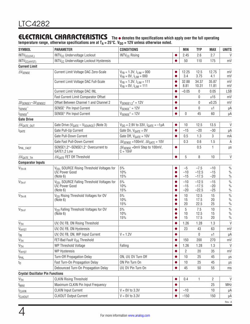
ELECTRICAL CHARACTERISTICS The l denotes the specifications which apply over the full operating temperature range, otherwise specifications are at TA = 25°C. VDD = 12V unless otherwise noted.
LTC4282
4Rev. A
For more information www.analog.com
ELECTRICAL CHARACTERISTICS The l denotes the specifications which apply over the full operating temperature range, otherwise specifications are at TA = 25°C. VDD = 12V unless otherwise noted.
SYMBOL PARAMETER CONDITIONS MIN TYP MAX UNITSINTVCC(UVL) INTVCC Undervoltage Lockout INTVCC Rising l 2.45 2.6 2.7 VINTVCC(HYST) INTVCC Undervoltage Lockout Hysteresis l 50 110 175 mVCurrent Limit∆VSENSE Current Limit Voltage DAC Zero-Scale VFB = 1.3V, ILIM = 000
VFB = 0V, ILIM = 000l
l
12.25 3.4
12.5 3.75
12.75 4.1
mV mV
Current Limit Voltage DAC Full-Scale VFB = 1.3V, ILIM = 111 VFB = 0V, ILIM = 111
l
l
32.88 8.81
34.37 10.31
35.87 11.81
mV mV
Current Limit Voltage DAC INL l –0.05 0 0.05 LSBFast Current Limit Comparator Offset l 0 ±15 mV
∆VSENSE1–∆VSENSE2 Offset Between Channel 1 and Channel 2 VSENSE1,2+ = 12V l 0 ±0.25 mV
ISENSE– SENSE– Pin Input Current VSENSE
– = 12V l 0 ±1 µAISENSE
+ SENSE+ Pin Input Current VSENSE+ = 12V l 0 45 60 µA
Gate Drive∆VGATE_OUT Gate Drive (VGATE – VSOURCE) (Note 3) VDD = 2.9V to 33V, IGATE = –1µA l 10 12.5 13.5 VIGATE Gate Pull-Up Current Gate On, VGATE = 0V l –15 –20 –30 µA
Gate Pull-Down Current Gate Off, VGATE = 10V l 0.5 1.3 3 mAGate Fast Pull-Down Current ∆VSENSE =100mV, ∆VGATE = 10V 0.3 0.6 1.5 A
tPHL_FAST SENSE1,2+–SENSE1,2– Overcurrent to GATE1,2 Low
∆VSENSE =0mV Step to 100mV, C = 10nF
l 0.5 1 µs
∆VGATE_TH ∆VGATE FET Off Threshold l 5 8 10 VComparator InputsVTH-R VDD, SOURCE Rising Threshold Voltages for
UV, Power Good (Note 6)
5% 10% 15%
l
l
l
–5 –10 –15
–7.5 –12.5 –17.5
–10 –15 –20
% % %
VTH-F VDD, SOURCE Falling Threshold Voltages for UV, Power Good (Note 6)
5% 10% 15%
l
l
l
–10 –15 –20
–12.5 –17.5 –22.5
–15 –20 –25
% % %
VTH-R VDD Rising Threshold Voltages for OV (Note 6)
5% 10% 15%
l
l
l
10 15 20
12.5 17.5 22.5
15 20 25
% % %
VTH-F VDD Falling Threshold Voltages for OV (Note 6)
5% 10% 15%
l
l
l
5 10 15
7.5 12.5 17.5
10 15 20
% % %
VTH UV, OV, FB, ON Rising Threshold l 1.26 1.28 1.3 VVHYST UV, OV, FB, ON Hysteresis l 23 43 63 mVIIN UV, OV, FB, ON, WP Input Current V = 1.2V l 0 ±1 µAVTH FET-Bad Fault VDS Threshold l 150 200 270 mVVTH WP Threshold Voltage Falling l 1.26 1.28 1.3 VVHYST WP Hysteresis l 2 20 35 mVtPHL Turn-Off Propagation Delay ON, UV, OV Turn Off l 10 25 45 µstD Fast Turn-On Propagation Delay ON Pin Turn On l 10 25 45 µs
Debounced Turn-On Propagation Delay UV, OV Pin Turn On l 45 50 55 msCrystal Oscillator Pin FunctionsVTH CLKIN Rising Threshold l 0.4 1 2 VfMAX Maximum CLKIN Pin Input Frequency l 25 MHzICLKIN CLKIN Input Current V = 0V to 3.3V l –10 10 µAICLKOUT CLKOUT Output Current V = 0V to 3.3V l –150 150 µA
LTC4282
5Rev. A
For more information www.analog.com
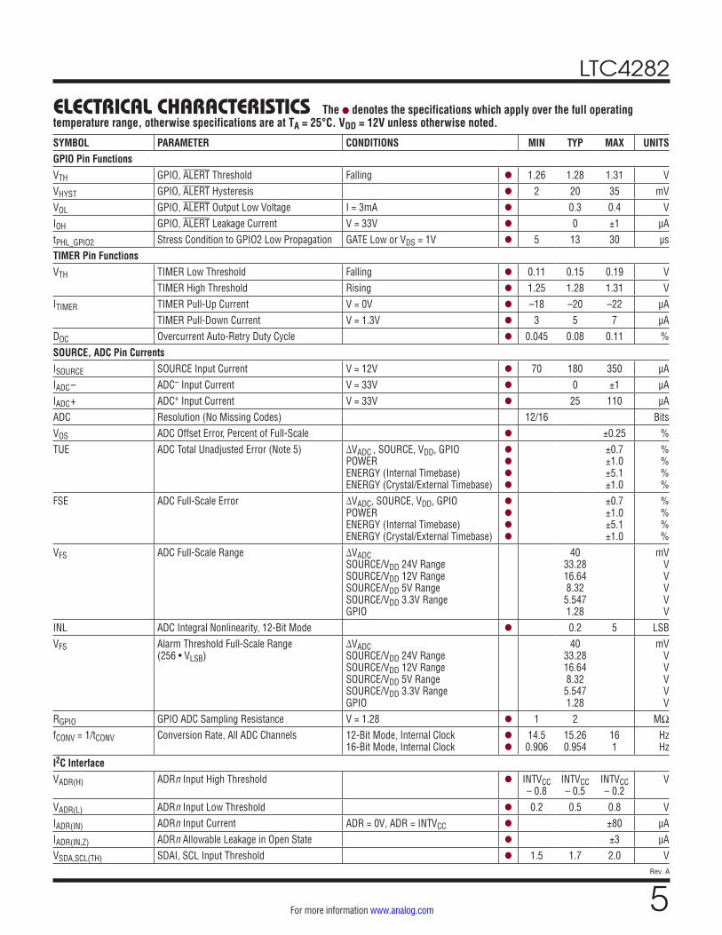
ELECTRICAL CHARACTERISTICS The l denotes the specifications which apply over the full operating temperature range, otherwise specifications are at TA = 25°C. VDD = 12V unless otherwise noted.
SYMBOL PARAMETER CONDITIONS MIN TYP MAX UNITSGPIO Pin FunctionsVTH GPIO, ALERT Threshold Falling l 1.26 1.28 1.31 VVHYST GPIO, ALERT Hysteresis l 2 20 35 mVVOL GPIO, ALERT Output Low Voltage I = 3mA l 0.3 0.4 VIOH GPIO, ALERT Leakage Current V = 33V l 0 ±1 µAtPHL_GPIO2 Stress Condition to GPIO2 Low Propagation GATE Low or VDS = 1V l 5 13 30 µsTIMER Pin FunctionsVTH TIMER Low Threshold Falling l 0.11 0.15 0.19 V
TIMER High Threshold Rising l 1.25 1.28 1.31 VITIMER TIMER Pull-Up Current V = 0V l –18 –20 –22 µA
TIMER Pull-Down Current V = 1.3V l 3 5 7 µADOC Overcurrent Auto-Retry Duty Cycle l 0.045 0.08 0.11 %SOURCE, ADC Pin CurrentsISOURCE SOURCE Input Current V = 12V l 70 180 350 µAIADC– ADC– Input Current V = 33V l 0 ±1 µAIADC+ ADC+ Input Current V = 33V l 25 110 µAADC Resolution (No Missing Codes) 12/16 BitsVOS ADC Offset Error, Percent of Full-Scale l ±0.25 %TUE ADC Total Unadjusted Error (Note 5) ∆VADC
, SOURCE, VDD, GPIO POWER ENERGY (Internal Timebase) ENERGY (Crystal/External Timebase)
l
l
l
l
±0.7 ±1.0 ±5.1 ±1.0
% % % %
FSE ADC Full-Scale Error ∆VADC, SOURCE, VDD, GPIO POWER ENERGY (Internal Timebase) ENERGY (Crystal/External Timebase)
l
l
l
l
±0.7 ±1.0 ±5.1 ±1.0
% % % %
VFS ADC Full-Scale Range ∆VADC
SOURCE/VDD 24V Range SOURCE/VDD 12V Range SOURCE/VDD 5V Range SOURCE/VDD 3.3V Range GPIO
40 33.28 16.64 8.32 5.547 1.28
mV V V V V V
INL ADC Integral Nonlinearity, 12-Bit Mode l 0.2 5 LSBVFS Alarm Threshold Full-Scale Range
(256 • VLSB)∆VADC
SOURCE/VDD 24V Range SOURCE/VDD 12V Range SOURCE/VDD 5V Range SOURCE/VDD 3.3V Range GPIO
40 33.28 16.64 8.32 5.547 1.28
mV V V V V V
RGPIO GPIO ADC Sampling Resistance V = 1.28 l 1 2 MΩfCONV = 1/tCONV Conversion Rate, All ADC Channels 12-Bit Mode, Internal Clock
16-Bit Mode, Internal Clockl
l
14.5 0.906
15.26 0.954
16 1
Hz Hz
I2C InterfaceVADR(H) ADRn Input High Threshold l INTVCC
– 0.8INTVCC – 0.5
INTVCC – 0.2
V
VADR(L) ADRn Input Low Threshold l 0.2 0.5 0.8 VIADR(IN) ADRn Input Current ADR = 0V, ADR = INTVCC l ±80 µAIADR(IN,Z) ADRn Allowable Leakage in Open State l ±3 µAVSDA,SCL(TH) SDAI, SCL Input Threshold l 1.5 1.7 2.0 V
LTC4282
6Rev. A
For more information www.analog.com
ELECTRICAL CHARACTERISTICS The l denotes the specifications which apply over the full operating temperature range, otherwise specifications are at TA = 25°C. VDD = 12V unless otherwise noted.
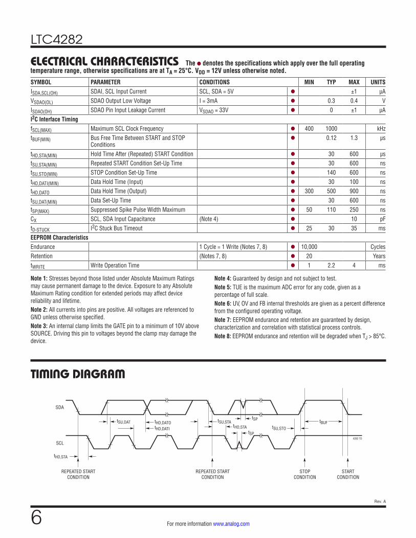
SYMBOL PARAMETER CONDITIONS MIN TYP MAX UNITSISDA,SCL(OH) SDAI, SCL Input Current SCL, SDA = 5V l ±1 µAVSDAO(OL) SDAO Output Low Voltage I = 3mA l 0.3 0.4 VISDAO(OH) SDAO Pin Input Leakage Current VSDAO = 33V l 0 ±1 µAI2C Interface TimingfSCL(MAX) Maximum SCL Clock Frequency l 400 1000 kHztBUF(MIN) Bus Free Time Between START and STOP
Conditionsl 0.12 1.3 µs
tHD,STA(MIN) Hold Time After (Repeated) START Condition l 30 600 µstSU,STA(MIN) Repeated START Condition Set-Up Time l 30 600 nstSU,STO(MIN) STOP Condition Set-Up Time l 140 600 nstHD,DATI(MIN) Data Hold Time (Input) l 30 100 nstHD,DATO Data Hold Time (Output) l 300 500 900 nstSU,DAT(MIN) Data Set-Up Time l 30 600 nstSP(MAX) Suppressed Spike Pulse Width Maximum l 50 110 250 nsCX SCL, SDA Input Capacitance (Note 4) l 10 pFtD-STUCK I2C Stuck Bus Timeout l 25 30 35 msEEPROM CharacteristicsEndurance 1 Cycle = 1 Write (Notes 7, 8) l 10,000 CyclesRetention (Notes 7, 8) l 20 YearstWRITE Write Operation Time l 1 2.2 4 ms
Note 1: Stresses beyond those listed under Absolute Maximum Ratings may cause permanent damage to the device. Exposure to any Absolute Maximum Rating condition for extended periods may affect device reliability and lifetime.Note 2: All currents into pins are positive. All voltages are referenced to GND unless otherwise specified.Note 3: An internal clamp limits the GATE pin to a minimum of 10V above SOURCE. Driving this pin to voltages beyond the clamp may damage the device.
Note 4: Guaranteed by design and not subject to test.Note 5: TUE is the maximum ADC error for any code, given as a percentage of full scale.Note 6: UV, OV and FB internal thresholds are given as a percent difference from the configured operating voltage.Note 7: EEPROM endurance and retention are guaranteed by design, characterization and correlation with statistical process controls. Note 8: EEPROM endurance and retention will be degraded when TJ > 85°C.
tSP
tBUFtSU,STO
tSP
tHD,STA
STARTCONDITION
STOPCONDITION
tSU,STAtHD,DATI
tHD,DATO
REPEATED STARTCONDITION
REPEATED STARTCONDITION
tSU,DAT
SDA
SCL
tHD,STA
4282 TD
TIMING DIAGRAM
LTC4282
7Rev. A
For more information www.analog.com
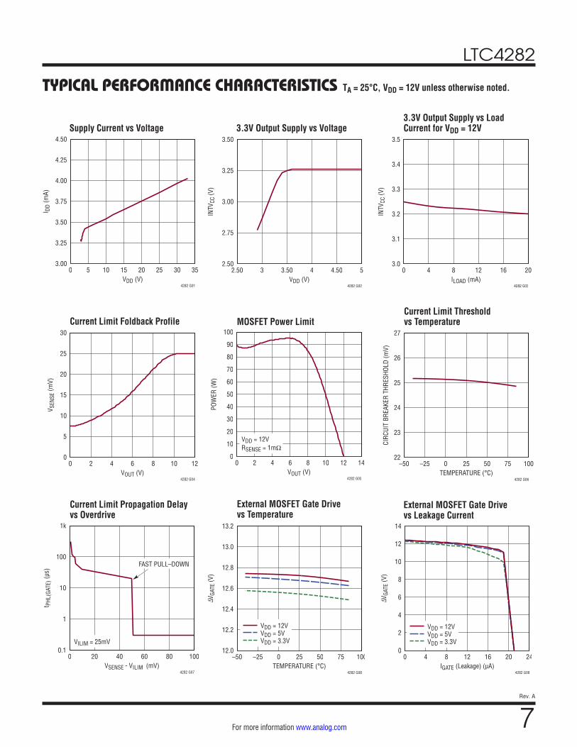
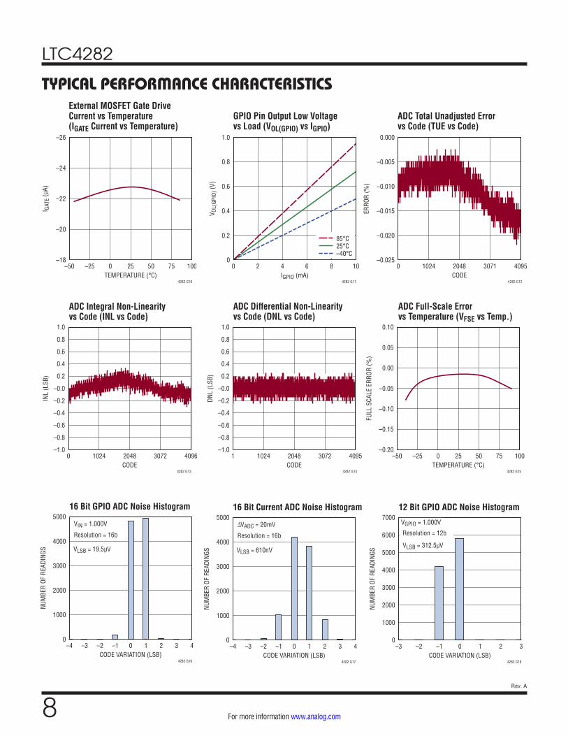
TYPICAL PERFORMANCE CHARACTERISTICS
Current Limit Foldback Profile MOSFET Power LimitCurrent Limit Threshold vs Temperature
Current Limit Propagation Delay vs Overdrive
Supply Current vs Voltage 3.3V Output Supply vs Voltage3.3V Output Supply vs Load Current for VDD = 12V
TA = 25°C, VDD = 12V unless otherwise noted.
External MOSFET Gate Drive vs Leakage Current
External MOSFET Gate Drive vs Temperature
VDD (V)0 5 10 15 20 25 30 35
3.00
3.25
3.50
3.75
4.00
4.25
4.50
I DD
(mA)
4282 G01VDD (V)
2.50 3 3.50 4 4.50 52.50
2.75
3.00
3.25
3.50
INTV
CC (V
)
4282 G02ILOAD (mA)
0 4 8 12 16 203.0
3.1
3.2
3.3
3.4
3.5
INTV
CC (V
)
4282 G03
VOUT (V)0 2 4 6 8 10 12
0
5
10
15
20
25
30
V SEN
SE (m
V)
4282 G04
RSENSE = 1mΩVDD = 12V
VOUT (V)0 2 4 6 8 10 12 14
0
10
20
30
40
50
60
70
80
90
100
POW
ER (W
)
4282 G05TEMPERATURE (°C)
–50 –25 0 25 50 75 10022
23
24
25
26
27
CIRC
UIT
BREA
KER
THRE
SHOL
D (m
V)
4282 G06
FAST PULL–DOWN
VILIM = 25mV
VSENSE - VILIM (mV)0 20 40 60 80 100
0.1
1
10
100
1k
t PHL
(GAT
E) (µ
s)
4282 G07
VDD = 12VVDD = 5VVDD = 3.3V
TEMPERATURE (°C)–50 –25 0 25 50 75 100
12.0
12.2
12.4
12.6
12.8
13.0
13.2
∆VGA
TE (V
)
4282 G08
VDD = 12VVDD = 5VVDD = 3.3V
IGATE (Leakage) (µA)0 4 8 12 16 20 24
0
2
4
6
8
10
12
14
∆VGA
TE (V
)
4282 G09
LTC4282
8Rev. A
For more information www.analog.com
TYPICAL PERFORMANCE CHARACTERISTICS
GPIO Pin Output Low Voltage vs Load (VOL(GPIO) vs IGPIO)
ADC Total Unadjusted Error vs Code (TUE vs Code)
ADC Integral Non-Linearity vs Code (INL vs Code)
ADC Differential Non-Linearity vs Code (DNL vs Code)
ADC Full-Scale Error vs Temperature (VFSE vs Temp.)
External MOSFET Gate Drive Current vs Temperature (IGATE Current vs Temperature)
TEMPERATURE (°C)–50 –25 0 25 50 75 100
–18
–20
–22
–24
–26
I GAT
E (µ
A)
4282 G10
85°C25°C–40°C
IGPIO (mA)0 2 4 6 8 10
0
0.2
0.4
0.6
0.8
1.0
V OL(
GPIO
) (V)
4282 G11CODE
0 1024 2048 3071 4095–0.025
–0.020
–0.015
–0.010
–0.005
0.000
ERRO
R (%
)
4282 G12
CODE0 1024 2048 3072 4096
–1.0
–0.8
–0.6
–0.4
–0.2
–0.0
0.2
0.4
0.6
0.8
1.0
INL
(LSB
)
4282 G13
Right Click In Graph Area for MenuDouble Click In Graph Area for Data Setup
CODE1 1024 2048 3072 4095
–1.0
–0.8
–0.6
–0.4
–0.2
–0.0
0.2
0.4
0.6
0.8
1.0
DNL
(LSB
)
4282 G14TEMPERATURE (°C)
–50 –25 0 25 50 75 100–0.20
–0.15
–0.10
–0.05
0.00
0.05
0.10
FULL
SCA
LE E
RROR
(%)
4282 G15
VIN = 1.000V
Resolution = 16b
VLSB = 19.5µV
CODE VARIATION (LSB)–4 –3 –2 –1 0 1 2 3 4
0
1000
2000
3000
4000
5000
NUM
BER
OF R
EADI
NGS
16 Bit GPIO ADC Noise Histogram
4282 G16
∆VADC = 20mV
Resolution = 16b
VLSB = 610nV
CODE VARIATION (LSB)–4 –3 –2 –1 0 1 2 3 4
0
1000
2000
3000
4000
5000
NUM
BER
OF R
EADI
NGS
16 Bit Current ADC Noise Histogram
4282 G17
VGPIO = 1.000V
Resolution = 12b
VLSB = 312.5µV
CODE VARIATION (LSB)–3 –2 –1 0 1 2 3
0
1000
2000
3000
4000
5000
6000
7000
NUM
BER
OF R
EADI
NGS
12 Bit GPIO ADC Noise Histogram
4282 G18
LTC4282
9Rev. A
For more information www.analog.com
PIN FUNCTIONSADC+: Positive Kelvin ADC Current Sense Input. Use a resistive divider between the two SENSE+ pins to measure the average of the two SENSE+ voltages. Tie to SENSE1+ when using a single sense resistor. Must be connected to the same trace as VDD or a resistive averaging network which adds up to 1Ω to VDD.
ADC–: Negative Kelvin ADC Current Sense Input. Use a resistive divider between the two SENSE – pins to measure the average of the two SENSE– voltages. Tie to SENSE1–
when using a single sense resistor.
ADR0-ADR2: Serial Bus Address Inputs. Tying these pins to ground (L), open (NC), or INTVCC (H) configures one of 27 possible addresses. See Table 1 in Applications Information.
ALERT: I2C Bus ALERT Output or General Purpose Input/Output. Configurable to ALERT output, general purpose output or logic input. Tie to ground if unused.
CLKIN: Clock Input. Connect to an optional external crystal oscillator circuit or drive with an external clock. Connect to ground if unused.
CLKOUT: Clock Output. Connect to an optional external crystal oscillator circuit. Can be configured in non-volatile memory to output the internal clock or a low pulse when the ADC finishes a conversion. Float if unused.
FB: Foldback Current Limit and Power Good Input. A resistive divider from the output is tied to this pin. When the voltage at this pin drops below 1.28V, power is not considered good. The power bad condition may result in the GPIO1 pin pulling low or going high impedance depending on the configuration of GPIO_CONFIG register 0x07 bits 4 and 5, also a power bad fault is logged in this condition if the GATE pin is high. The start-up current limit folds back to 30% as the FB pin voltage drops from 1.3V to 0V.
GATE1, GATE2: Gate Drives for External N-Channel MOSFETs. Internal 20µA current sources charge the gates of the MOSFETs. No compensation capacitors are required on the GATE pins, but a resistor and capaci-tor network from these pins to ground may be used to set the turn-on output voltage slew rate. During turn-off there is a 1mA pull-down current. During a short-circuit or undervoltage lockout (VDD or INTVCC), a 600mA pull-down between GATE1/GATE2 and SOURCE is activated. Tie both GATE pins together if only one MOSFET is used and SENSE2– is grounded.
GND: Device Ground.
GPIO1: General Purpose Input/Open-Drain Output. Configurable to general purpose output, logic input, and power good or power bad signal. Tie to ground if unused.
GPIO2: General Purpose Input/Open-Drain Output. Configurable to general purpose output, logic input, MOSFET stress output, and data converter input. Tie to ground if unused.
GPIO3: General Purpose Input/Open-Drain Output. Configurable to general purpose output, logic input, and data converter input. Tie to ground if unused.
INTVCC: 3.3V Supply Decoupling Output. Connect a 1μF capacitor from this pin to ground. To ensure fault log-ging after power is lost a 4.7μF capacitor should be used. 25mA may be drawn from this pin to power 3.3V applica-tion circuitry. Increase capacitance by 1µF/mA external load when fault logging is used. This pin should not be driven and is not current limited.
NC: No Connect.
ON: On Control Input. Used to monitor a connection sense pin on the backplane connector. The default polarity is high = on, but may be reconfigured to low = on by setting CONTROL1 register 0x00 bit 5 low. An on-to-off transition on this pin clears the fault register if CONTROL1 register 0x00 bit 7 is set high. The ON pin has a precise 1.28V threshold, allowing it to double as a supply monitor.
LTC4282
10Rev. A
For more information www.analog.com
PIN FUNCTIONSSENSE– pins to the value selected in the ILIM register or less. Tie SENSE2– to GND when unused.
SOURCE: N-Channel MOSFET Source and ADC Input. Connect this pin to the source of the external N-channel MOSFET. This pin provides a return for the GATE pull-down circuit and also serves as the ADC input to monitor the output voltage.
TIMER: Current Limit and Retry Timer Input. Connect a capacitor between this pin and ground to set a 64ms/µF duration for current limit, after which an overcurrent fault is logged and GATE is pulled low. The duration of the off time is 73s/µF when overcurrent auto-retry is enabled, resulting in a 0.08% duty cycle.
UV: Undervoltage Input Pin. Connect a resistive divider when the internal divider is disabled. A capacitor may be placed on this pin to filter brief UV glitches on the input supply.
VDD: Supply Voltage Input and UV/OV Input. This pin has an undervoltage lockout threshold of 2.7V. The UV and OV thresholds are also measured at this pin, and the ADC may be configured to read the voltage at this pin.
WP: EEPROM Write Protect. All writes to the EEPROM except fault logging are blocked when WP is high.
OV: Overvoltage Input Pin. An overvoltage condition is present whenever this pin is above the configured thresh-old. Connect a resistive divider when the internal divider is disabled, otherwise leave open.
SCL: Serial Bus Clock Input. Data at the SDA pin is shifted in or out on rising edges of SCL. This is a high impedance pin that is driven by an open-drain output from a master controller. An external pull-up resistor or current source is required.
SDAI: Serial Bus Data Input. A high impedance input for shifting in address, command or data bits. Normally tied to SDAO to form the SDA line.
SDAO: Serial Bus Data Output. Open-drain output for sending data back to the master controller or acknowledg-ing a write operation. Normally tied to SDAI to form the SDA line. An external pull-up resistor or current source is required.
SENSE1+, SENSE2+: Positive Kelvin Current Sense Input. Connect this pin to the input side of the current sense resistor or an averaging network in the case of multiple sense resistors. The parallel resistance of an averaging network should not exceed 1Ω. Must operate at the same potential as VDD.
SENSE1–, SENSE2– : Negative Kelvin Current Sense Input. Connect this pin to the output side of the current sense resistor. The current limit circuit controls the GATE pin to limit the sense voltage between the SENSE+ and
LTC4282
11Rev. A
For more information www.analog.com
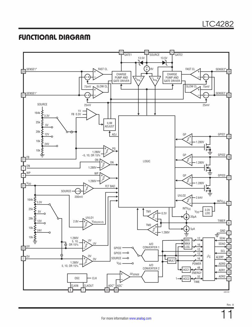
FUNCTIONAL DIAGRAM
+–
+–
+–
+–
+–
+–
ADR2321
∆VSENSE
UVLO1
OVOV
UV
24V
OV
2.8V
1.280V5, 10, OR 15%
1.280V–5, 10, OR 15%
1.280V5, 10,
OR 15%
VDD(UVLO)
11
2
ADC–ADC+
26CLKOUT
CLK
7CLKIN
8 30
32
ADR110
ADR09
ALERT15
SCL14
SDAO13
SDAI12
TIMER
INTVCC
6
GP
1.280V
GPIO119
SENSE2+
SENSE2–
GND3
I2C
ACC2TIME
4282 BD
48
16
12
ACC1
MULT
MINMAXLOG
ENERGY
16
1212
POWER
A/DCONVERTER 1
A/DCONVERTER 2
GPIO2
GPIO3
SOURCE
VDD
+–
+–
12V
5V
3.3V
24V
12V
5V
3.3V
10k
10k
28k
25k
164k
SOURCE
200mV
1.280V
FET BAD
WP
VDD
+–
UVUV
31
WP4
+–1.280V
ONON
PG
ADJ
1V FB 0.3V
ON1
+–
FB21
SOURCE
27
SENSE1+
SENSE1–
29
TM10.2V
20µA
5µA1.280V
+–
TM2
ILIMADJUST
3.3VLDO
OSC
+–
GP
1.280V
GPIO218
+–
GP
LOGIC
1.280V
GPIO317
+–
UVLO22.64V
VDD
INTVCC 5
24GATE2
FAST CL
75mV75mV
25mV25mV
SLOW CL
23GATE1
+ – +–
22
+–
SOURCE
CHARGEPUMP AND
GATE DRIVER
CHARGEPUMP AND
GATE DRIVER
8V
13.5V13.5V
+–
+–
+–
+–
FAST CL
SLOW CL
+–
+–
+–
+– 25
28
10k
10k
28k
25k
164k
LTC4282
12Rev. A
For more information www.analog.com
OPERATIONThe LTC4282 is designed to turn a board’s supply voltage on and off in a controlled manner, allowing the board to be safely inserted or removed from a live backplane. During normal operation, the gate drivers turn on a pair of parallel external N-channel MOSFETs to pass power to the load. The gate driver charge pumps derive their power from the VDD pin. Also included in the gate drivers are 12.5V GATE-to-SOURCE clamps to protect the oxide of external MOSFETs. During start-up the inrush current is tightly balanced and controlled by using current limit foldback.
Two MOSFETs are used to double the SOA and halve the RDS(ON) as compared to a single MOSFET. The current limit (CL) amplifiers monitor the load current with cur-rent sense resistors connected between the SENSE1+, SENSE2+ and SENSE1–, SENSE2– pins. The CL amplifiers limit the current in the load by pulling back on the GATE-to-SOURCE voltages in an active control loop when the sense voltages exceed the commanded value.
An overcurrent fault at the output may result in excessive MOSFET power dissipation during active current limiting. To limit this power, the CL amplifiers regulate the voltage between the SENSE1+, SENSE2+ and SENSE1–, SENSE2– pins at the value set in the ILIM register. When the output (SOURCE pin) is low, power dissipation is further reduced by folding back the current limit to 30% of nominal.
The TIMER pin ramps up with 20μA when both current limit circuits are active. The LTC4282 turns off both GATEs and registers a fault when the TIMER pin reaches its 1.28V threshold. At this point the TIMER pin ramps down using a 5μA current source until the voltage drops below 0.2V (comparator TM1). The TIMER pin will then ramp up and down 256 times with 20µA/5µA before indicating that the external MOSFET has cooled and it is safe to turn on again, provided overcurrent auto-retry is enabled.
The output voltage is monitored using the SOURCE pin and the power good (PG) comparator to determine if the power is available for the load. The power good condi-tion can be signaled by the GPIO1 pin. The GPIO1 pin may also be configured to signal power bad, as a general purpose input (GP comparator), or a general purpose open-drain output.
GPIO2 and GPIO3 may also be configured as general purpose inputs or general purpose open-drain outputs. Additionally the ADC measures these pins with a 1.28V full-scale. GPIO2 may be configured to pull low to indicate that the external MOSFETs are in a state of stress when the MOSFETs are commanded to be on and either the gate voltages are lower than they should be, or the drain-to-source voltage exceeds 200mV.
The Functional Diagram shows the monitoring blocks of the LTC4282. The group of comparators on the left side includes the undervoltage (UV), overvoltage (OV), and (ON) comparators. These comparators determine if the external conditions are valid prior to turning on the GATEs. But first the two undervoltage lockout circuits, UVLO1 and UVLO2, validate the input supply and the internally generated 3.3V supply, INTVCC. UVLO2 also generates the power-up initialization to the logic circuits and copies the contents of the EEPROM to operating memory after INTVCC crosses this rising threshold.
Included in the LTC4282 is a pair of 12-/16-bit A/D con-verters. One data converter continuously monitors the ADC+ to ADC– voltage, sampling every 16µs and produc-ing a 12-bit result of the average current sense voltage every 65ms. The other data converter is synchronized to the first one and measures the GPIO voltage and SOURCE voltage during the same time period. Every time the ADCs finish taking a measurement, the current sense voltage is multiplied by the measurement of the SOURCE pin to provide a power measurement. Every time power is mea-sured, it is added to an energy accumulator which keeps track of how much energy has been transmitted to the load. The energy accumulator can generate an optional alert upon overflow, and can be pre-set to allow it to over-flow after a given amount of energy has been transmit-ted. A time accumulator also keeps track of how many times the power meter has been incremented; dividing the results of the energy accumulator by the time accu-mulator gives the average system power. The minimum and maximum measurements of GPIO, SOURCE, ADC+ to ADC– and power are stored, and optional alerts may be generated if a measurement is above or below user configurable 8-bit thresholds.
LTC4282
13Rev. A
For more information www.analog.com
OPERATION
APPLICATIONS INFORMATION
An internal EEPROM provides nonvolatile configuration of the LTC4282’s behavior, records fault information and provides 4 bytes of uncommitted memory for general purpose storage.
An I2C interface is provided to read the A/D data registers. It also allows the host to poll the device and determine if
faults have occurred. If the ALERT pin is configured as an ALERT interrupt, the host is enabled to respond to faults in real time. The I2C device address is decoded using the ADR0-ADR2 pins. These inputs have three states each that decode into a total of 27 device addresses, as shown in Table 1.
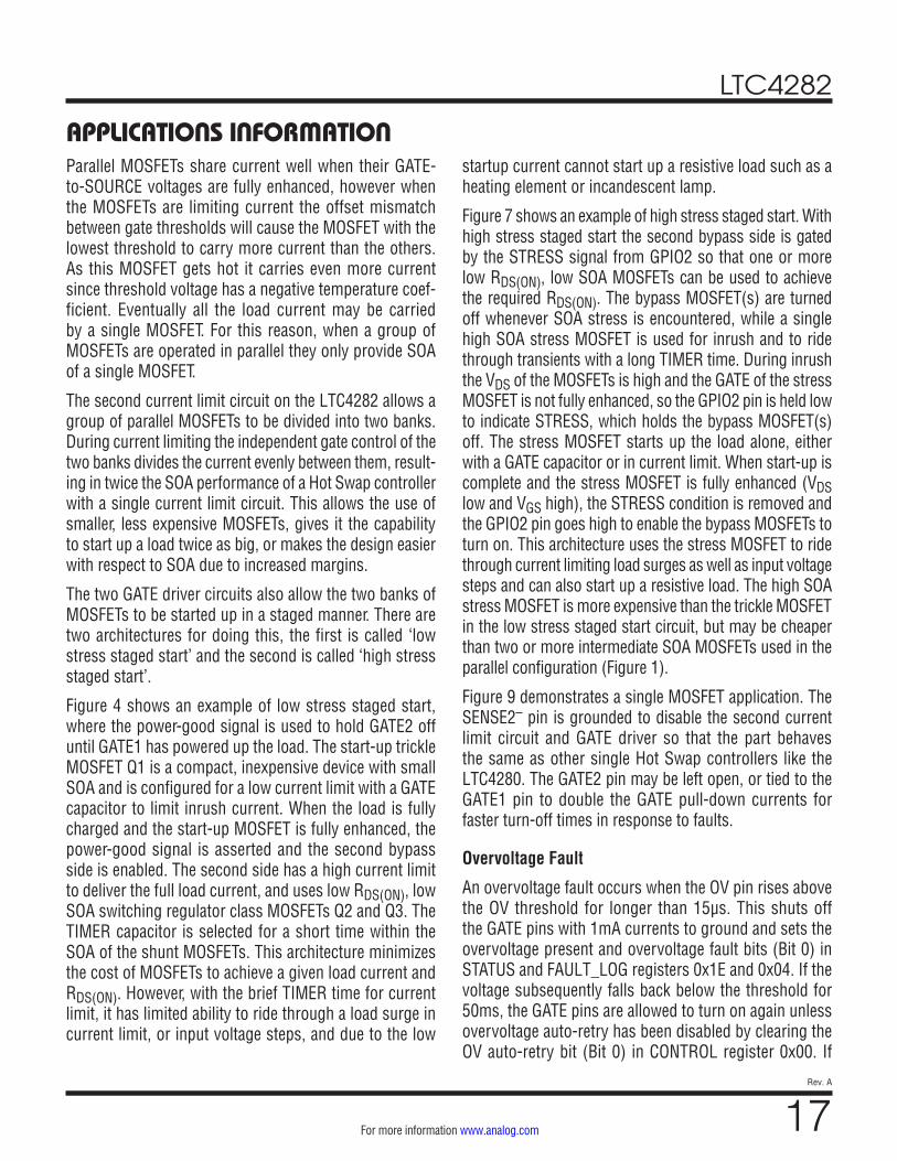
A typical LTC4282 application is a high availability system in which a positive voltage supply is distributed to power individual hot-swapped cards. The device measures card voltages and currents and records past and present fault conditions. The LTC4282 stores min and max ADC mea-surements, calculates power and energy, and can be con-figured to generate alerts based on measurement results, avoiding the need for the system to poll the device on a regular basis. The LTC4282 is configured with nonvolatile EEPROM memory, allowing it to be configured during board level testing and avoid having to configure the Hot Swap controller at every insertion.
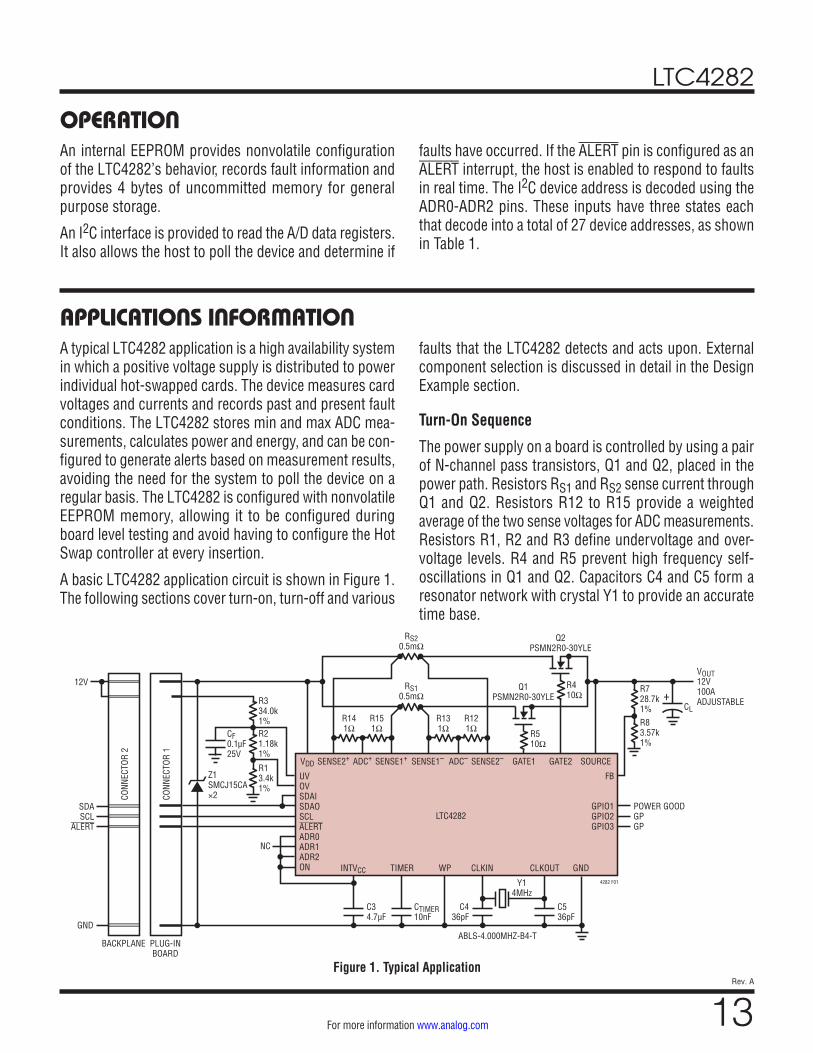
A basic LTC4282 application circuit is shown in Figure 1. The following sections cover turn-on, turn-off and various
faults that the LTC4282 detects and acts upon. External component selection is discussed in detail in the Design Example section.
Turn-On Sequence
The power supply on a board is controlled by using a pair of N-channel pass transistors, Q1 and Q2, placed in the power path. Resistors RS1 and RS2 sense current through Q1 and Q2. Resistors R12 to R15 provide a weighted average of the two sense voltages for ADC measurements. Resistors R1, R2 and R3 define undervoltage and over-voltage levels. R4 and R5 prevent high frequency self-oscillations in Q1 and Q2. Capacitors C4 and C5 form a resonator network with crystal Y1 to provide an accurate time base.
Figure 1. Typical Application
+
VDDZ1SMCJ15CA×2
GATE1 GATE2
CTIMER10nF
TIMER
LTC4282
INTVCC
CONN
ECTO
R 1
CONN
ECTO
R 2
PLUG-INBOARD
NC
4282 F01
GND
SDASCL
ALERT
R510Ω
CL
R410Ω
R728.7k1%R83.57k1%
VOUT12V100AADJUSTABLE
RS20.5mΩ
RS10.5mΩ
SOURCE
FB
GPIO1GPIO2GPIO3
POWER GOODGPGP
UVOVSDAISDAOSCLALERTADR0ADR1ADR2ON
SENSE2+ SENSE1+ SENSE1– SENSE2–ADC+
R141Ω
R151Ω
R131Ω
R121Ω
Q1PSMN2R0-30YLE
Q2PSMN2R0-30YLE
ADC–
WP GNDCLKOUTCLKIN
Y14MHz
ABLS-4.000MHZ-B4-T
C34.7µF
C436pF
C536pF
12V
BACKPLANE
R21.18k1%
R334.0k1%
R13.4k1%
CF0.1µF25V
LTC4282
14Rev. A
For more information www.analog.com
Several conditions must be present before the external MOSFET turns on. First the external supply, VDD, must exceed its 2.7V undervoltage lockout level. Next the internally generated supply, INTVCC, must cross its 2.6V undervoltage threshold. This generates a 1ms power-on-reset pulse. During reset the fault registers are cleared and the control registers are loaded with the data held in the corresponding EEPROM registers.
After a power-on-reset pulse, the UV and OV pins verify that input power is within the acceptable range. The state of the UV and OV comparators is indicated by STATUS register 0x1E bits 1 and 2 and must be stable for at least 50ms to qualify for turn-on. The ON pin is checked to see that a connection sense ("short”) pin has asserted to the correct state. By default the ON pin has no delay, but a 50ms de-bounce delay may be added by setting CONTROL register 0x00 bit 6 high. When these conditions are sat-isfied, turn-on is initiated. Figure 10 shows connection sense configurations for both high- and low-going short pins. The ON pin has a precise 1.28V threshold, allowing it to also monitor a voltage through the short pin, such as a house-keeping or auxiliary supply delivered by the backplane. Use of the UV/OV divider for short pin detec-tion in high current applications is not recommended, as voltage drops in the connector and fuse will impair the accuracy of the intended function.
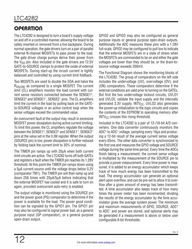
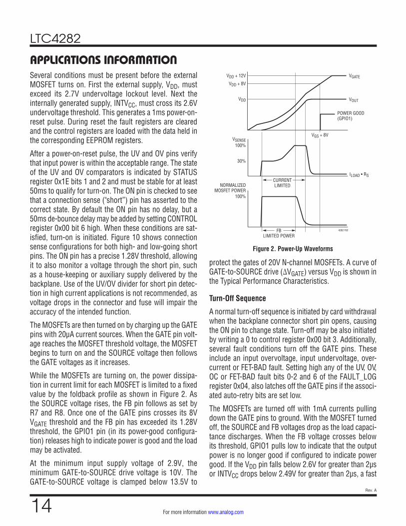
The MOSFETs are then turned on by charging up the GATE pins with 20μA current sources. When the GATE pin volt-age reaches the MOSFET threshold voltage, the MOSFET begins to turn on and the SOURCE voltage then follows the GATE voltages as it increases.
While the MOSFETs are turning on, the power dissipa-tion in current limit for each MOSFET is limited to a fixed value by the foldback profile as shown in Figure 2. As the SOURCE voltage rises, the FB pin follows as set by R7 and R8. Once one of the GATE pins crosses its 8V VGATE threshold and the FB pin has exceeded its 1.28V threshold, the GPIO1 pin (in its power-good configura-tion) releases high to indicate power is good and the load may be activated.
At the minimum input supply voltage of 2.9V, the minimum GATE-to-SOURCE drive voltage is 10V. The GATE-to-SOURCE voltage is clamped below 13.5V to
protect the gates of 20V N-channel MOSFETs. A curve of GATE-to-SOURCE drive (∆VGATE) versus VDD is shown in the Typical Performance Characteristics.
Turn-Off Sequence
A normal turn-off sequence is initiated by card withdrawal when the backplane connector short pin opens, causing the ON pin to change state. Turn-off may be also initiated by writing a 0 to control register 0x00 bit 3. Additionally, several fault conditions turn off the GATE pins. These include an input overvoltage, input undervoltage, over-current or FET-BAD fault. Setting high any of the UV, OV, OC or FET-BAD fault bits 0-2 and 6 of the FAULT_LOG register 0x04, also latches off the GATE pins if the associ-ated auto-retry bits are set low.
The MOSFETs are turned off with 1mA currents pulling down the GATE pins to ground. With the MOSFET turned off, the SOURCE and FB voltages drop as the load capaci-tance discharges. When the FB voltage crosses below its threshold, GPIO1 pulls low to indicate that the output power is no longer good if configured to indicate power good. If the VDD pin falls below 2.6V for greater than 2µs or INTVCC drops below 2.49V for greater than 2µs, a fast
APPLICATIONS INFORMATION
Figure 2. Power-Up Waveforms
VDD + 12V
VSENSE100%
NORMALIZEDMOSFET POWER
100%
4282 F02
30%
VGATE
VOUT
POWER GOOD(GPIO1)
ILOAD • RS
VDD + 8V
CURRENTLIMITED
FBLIMITED POWER
VDD
VGS = 8V
LTC4282
15Rev. A
For more information www.analog.com
shut down of the MOSFET is initiated. The GATE pins are then pulled down with 600mA currents to the SOURCE pin.
Current Limit Adjustment
The current limit sense voltage of the LTC4282 is adjust-able between 12.5mV and 34.4mV in 3.1mV steps via the I2C interface with bits 7-5 of the ILIM_ADJUST register 0x11. Default values are stored in the onboard EEPROM. This can be used to adjust the sense voltage to achieve a given current limit using the limited selection of stan-dard sense resistor values available around 1mΩ. It also allows the LTC4282 to reduce available current for light loads or increase it in anticipation of a surge. This feature also enables the use of board-trace as sense resistors by trimming the sense voltage to match measured copper resistance during final test. The measured copper resis-tance may be written to the undedicated scratch pad area of the EEPROM so that it is available to scale ADC current measurements.
Constant Current Start-Up Using GATE R-C Networks
An optional series resistor and capacitor network from GATE to GROUND (RG and CG in Figure 4) provides an inrush current less than the current limit by limiting the slew rate of the GATE pin, which pulls up with 20µA. The current limit timer will not run since the current limit is not engaged during startup so a small timer capacitor may be used, which allows the use of MOSFETs with smaller safe operating area. Power good will not signal until the FB pin crosses its threshold and the GATE-to-SOURCE voltages crosses their 8V thresholds which indicates the MOSFETs are fully enhanced. When both those conditions are met, the output voltage is suitable for the load to be turned on and the impedance back to the supply through the MOSFET is low. Power good is then asserted with the GPIO1 pin or read via the interface, signaling that it is safe to turn on downstream loads. A power-bad fault is not generated when starting up in this manner because the FB pin will cross its threshold before the GATE-to-SOURCE threshold is crossed. RG should be chosen such that IGATE • RG is less than the threshold of the MOSFET to avoid a current spike at the beginning of startup. Reducing RG degrades the stability of the current limit circuit, see Applications Information on Current Limit Stability. If a
value of RG is not found that produces a voltage less than the MOSFET threshold when the 20µA IGATE current flows through it, while also producing a stable current limit servo loop, CG may be charged with a diode during start-up in parallel with a large RG, such as 500kΩ, to discharge it when the part turns off (see Figure 4). For the staged-start architectures, an RC must be used on a trickle MOSFET and may be used on a STRESS MOSFET. In the parallel architecture, identical RC networks may be used on both MOSFETs. Bypass MOSFETs don’t need the current limiting function of an RC network, but an RC net-work may be used in low-stress staged start to improve the undershoot recovery time of the bypass MOSFET(s).
Current Limit Stability
For most applications the LTC4282 current limit loop is stable without additional components. However there are certain conditions where additional components may be needed to improve stability. The dominant pole of the current limit circuit is set by the capacitance at the gate of the external MOSFET, and larger gate capacitance makes the current limit loop more stable. Usually a total of 8nF GATE-to-SOURCE capacitance is sufficient for stability and is provided by inherent MOSFET CGS. The stability of the loop is degraded by reducing the size of the resistor on a gate RC network if one is used to limit start-up current as in Figure 4, which may necessitate additional GATE-to-SOURCE capacitance. Board level short-circuit testing is highly recommended as board layout can also affect transient performance. The worst-case condition for cur-rent limit stability occurs when the output is shorted to ground after a normal start-up.
Parasitic MOSFET Oscillations
Not all circuit oscillations can be ascribed to the cur-rent limit loop. Some higher frequency oscillations can arise from the MOSFETs themselves. There are two pos-sible parasitic oscillation mechanisms. The first type of oscillation occurs at high frequencies, typically above 1MHz. This high frequency oscillation is easily damped with gate resistors R4 and R5 as shown in Figure 1. In some applications, one may find that these resistors help in short-circuit transient recovery as well. However, too large of a resistor will slow down the turn-off time.
APPLICATIONS INFORMATION
LTC4282
16Rev. A
For more information www.analog.com
The recommended R4 and R5 range is between 5Ω and 500Ω. 10Ω provides stability without affecting turn-off time. These resistors must be located at the MOSFET package with no other components connected to the MOSFET gate pin.
A second type of parasitic oscillation occurs at frequen-cies between 200kHz and 800kHz when the MOSFET source is loaded with less than 10µF, and the drain is fed with an inductive impedance such as contributed by wiring inductance. To prevent this second type of oscilla-tion load the source with more than 10µF and bypass the input supply with a series 10Ω, 100nF snubber to ground.
Overcurrent Fault
The LTC4282 features an adjustable current limit with foldback that protects the MOSFETs from excessive load current. To protect the MOSFETs during active current limit, the available current is reduced as a function of the output voltage sensed by the FB pin such that the power dissipated by the MOSFET is constant. A graph in the Typical Performance Characteristics shows the current limit and power versus FB voltage.
An overcurrent fault occurs when the current limit cir-cuitry has been engaged for both MOSFETs for longer than the timeout delay set by the TIMER capacitor. Current limiting begins when the current sense voltage between the SENSE+ and SENSE– pins reaches the current limit level (which depends on foldback and the current limit configuration). The corresponding GATE pin is then pulled down and regulated in order to limit the current sense voltage to the current limit value. If this is only happen-ing with one GATE, the other MOSFET is still low imped-ance and is allowed to carry additional current. When both GATE pins are regulated in current limit, the circuit breaker time delay starts by charging the external timer capacitor from the TIMER pin with a 20µA pull-up current. If the TIMER pin reaches its 1.28V threshold, the external switches turn off with 1mA currents from GATE to ground. If one of the GATE pins stops current limiting before the TIMER pin reaches the 1.28V threshold, the TIMER pin will discharge with 5μA. For a given circuit breaker time
delay, tCB, the equation for setting the timing capacitor’s value is as follows:
CT = tCB • 0.016[μF/ms]
If an overcurrent fault is detected the MOSFET is turned off and the TIMER pin begins discharging with a 5µA pull-down current. When the TIMER pin reaches its 0.15V threshold, it will cycle up and down with 20µA and 5µA 256 times to allow the MOSFETs time to cool down. When automatically retrying, the resulting overcurrent duty cycle is 1:1140. The final time the TIMER pin falls below its 0.15V lower threshold the switches are allowed to turn on again if the overcurrent auto-retry bit is set or the overcurrent fault bit has been reset by the I2C interface.
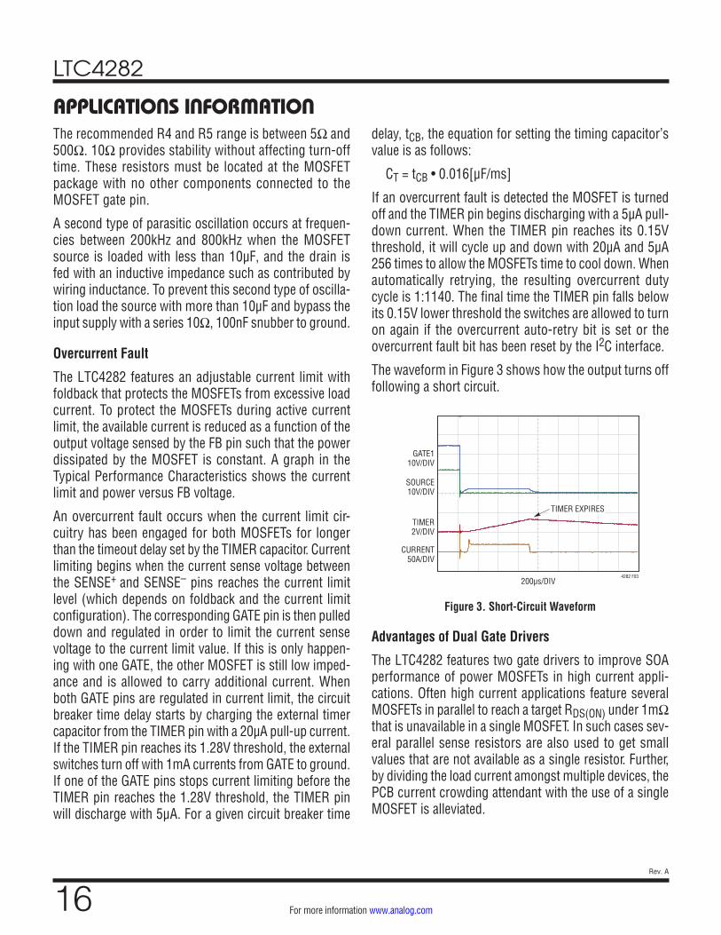
The waveform in Figure 3 shows how the output turns off following a short circuit.
Figure 3.
TIMER EXPIRES
200µs/DIV
TIMER2V/DIV
GATE110V/DIV
SOURCE10V/DIV
CURRENT50A/DIV
4282 F03
Short-Circuit Waveform
Advantages of Dual Gate Drivers
The LTC4282 features two gate drivers to improve SOA performance of power MOSFETs in high current appli-cations. Often high current applications feature several MOSFETs in parallel to reach a target RDS(ON) under 1mΩ that is unavailable in a single MOSFET. In such cases sev-eral parallel sense resistors are also used to get small values that are not available as a single resistor. Further, by dividing the load current amongst multiple devices, the PCB current crowding attendant with the use of a single MOSFET is alleviated.
APPLICATIONS INFORMATION
LTC4282
17Rev. A
For more information www.analog.com
APPLICATIONS INFORMATIONParallel MOSFETs share current well when their GATE-to-SOURCE voltages are fully enhanced, however when the MOSFETs are limiting current the offset mismatch between gate thresholds will cause the MOSFET with the lowest threshold to carry more current than the others. As this MOSFET gets hot it carries even more current since threshold voltage has a negative temperature coef-ficient. Eventually all the load current may be carried by a single MOSFET. For this reason, when a group of MOSFETs are operated in parallel they only provide SOA of a single MOSFET.
The second current limit circuit on the LTC4282 allows a group of parallel MOSFETs to be divided into two banks. During current limiting the independent gate control of the two banks divides the current evenly between them, result-ing in twice the SOA performance of a Hot Swap controller with a single current limit circuit. This allows the use of smaller, less expensive MOSFETs, gives it the capability to start up a load twice as big, or makes the design easier with respect to SOA due to increased margins.
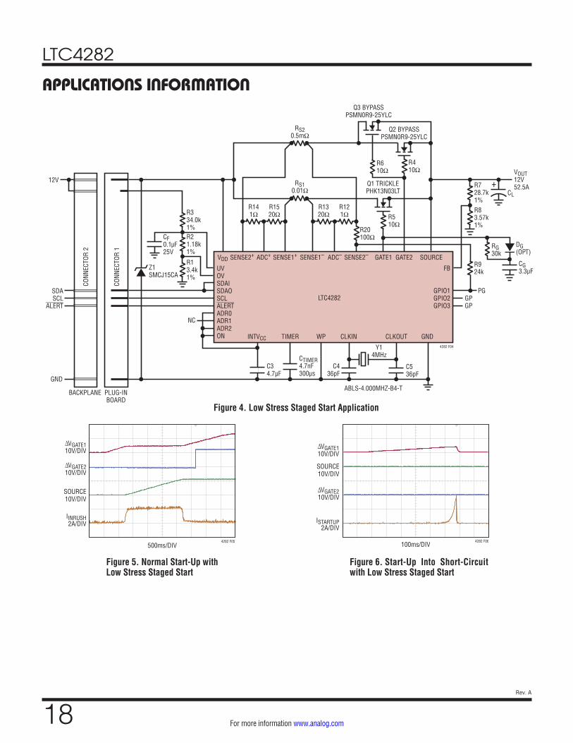
The two GATE driver circuits also allow the two banks of MOSFETs to be started up in a staged manner. There are two architectures for doing this, the first is called ‘low stress staged start’ and the second is called ‘high stress staged start’.
Figure 4 shows an example of low stress staged start, where the power-good signal is used to hold GATE2 off until GATE1 has powered up the load. The start-up trickle MOSFET Q1 is a compact, inexpensive device with small SOA and is configured for a low current limit with a GATE capacitor to limit inrush current. When the load is fully charged and the start-up MOSFET is fully enhanced, the power-good signal is asserted and the second bypass side is enabled. The second side has a high current limit to deliver the full load current, and uses low RDS(ON), low SOA switching regulator class MOSFETs Q2 and Q3. The TIMER capacitor is selected for a short time within the SOA of the shunt MOSFETs. This architecture minimizes the cost of MOSFETs to achieve a given load current and RDS(ON). However, with the brief TIMER time for current limit, it has limited ability to ride through a load surge in current limit, or input voltage steps, and due to the low
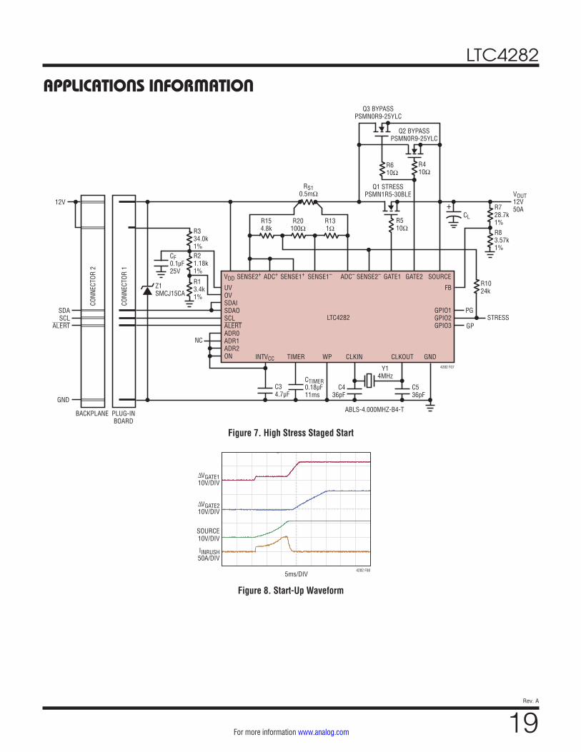
startup current cannot start up a resistive load such as a heating element or incandescent lamp.
Figure 7 shows an example of high stress staged start. With high stress staged start the second bypass side is gated by the STRESS signal from GPIO2 so that one or more low RDS(ON), low SOA MOSFETs can be used to achieve the required RDS(ON). The bypass MOSFET(s) are turned off whenever SOA stress is encountered, while a single high SOA stress MOSFET is used for inrush and to ride through transients with a long TIMER time. During inrush the VDS of the MOSFETs is high and the GATE of the stress MOSFET is not fully enhanced, so the GPIO2 pin is held low to indicate STRESS, which holds the bypass MOSFET(s) off. The stress MOSFET starts up the load alone, either with a GATE capacitor or in current limit. When start-up is complete and the stress MOSFET is fully enhanced (VDS low and VGS high), the STRESS condition is removed and the GPIO2 pin goes high to enable the bypass MOSFETs to turn on. This architecture uses the stress MOSFET to ride through current limiting load surges as well as input voltage steps and can also start up a resistive load. The high SOA stress MOSFET is more expensive than the trickle MOSFET in the low stress staged start circuit, but may be cheaper than two or more intermediate SOA MOSFETs used in the parallel configuration (Figure 1).
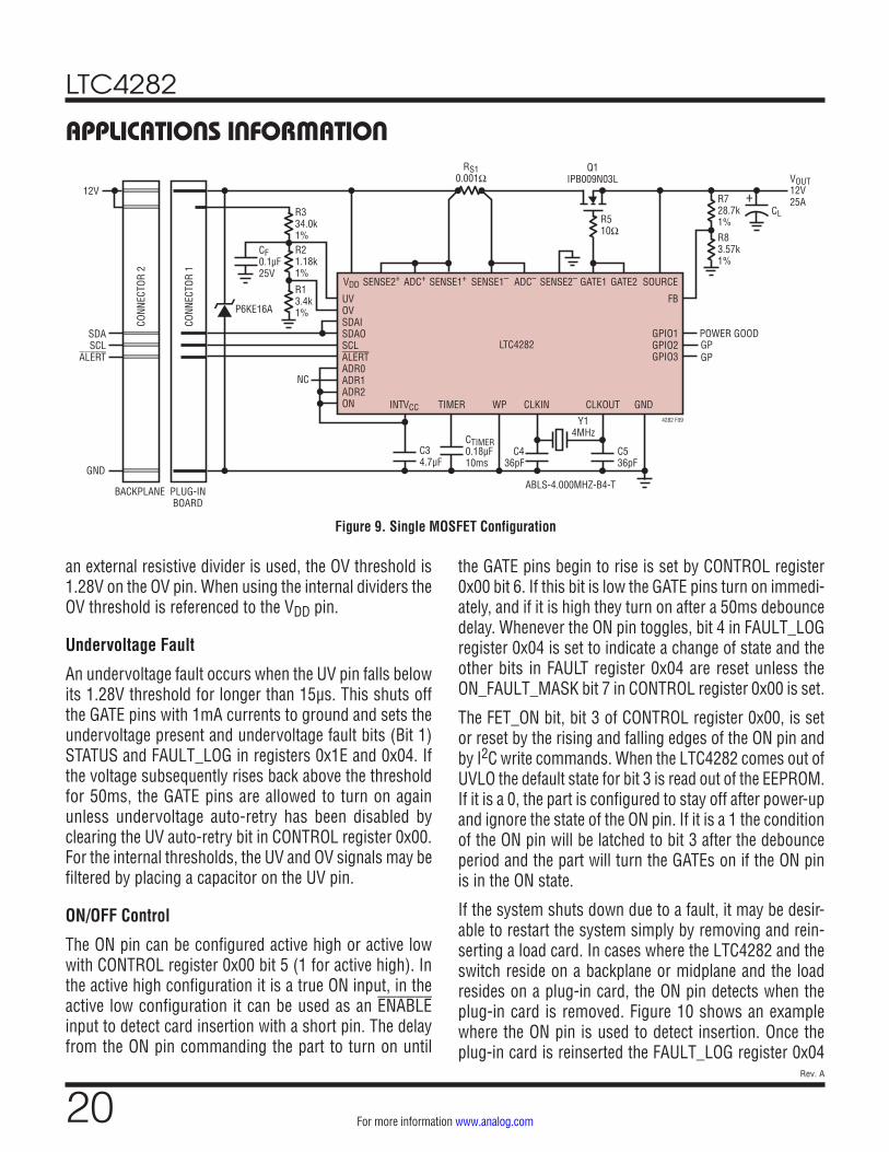
Figure 9 demonstrates a single MOSFET application. The SENSE2– pin is grounded to disable the second current limit circuit and GATE driver so that the part behaves the same as other single Hot Swap controllers like the LTC4280. The GATE2 pin may be left open, or tied to the GATE1 pin to double the GATE pull-down currents for faster turn-off times in response to faults.
Overvoltage Fault
An overvoltage fault occurs when the OV pin rises above the OV threshold for longer than 15µs. This shuts off the GATE pins with 1mA currents to ground and sets the overvoltage present and overvoltage fault bits (Bit 0) in STATUS and FAULT_LOG registers 0x1E and 0x04. If the voltage subsequently falls back below the threshold for 50ms, the GATE pins are allowed to turn on again unless overvoltage auto-retry has been disabled by clearing the OV auto-retry bit (Bit 0) in CONTROL register 0x00. If
LTC4282
18Rev. A
For more information www.analog.com
APPLICATIONS INFORMATION
Figure 4. Low Stress Staged Start Application
+
VDDZ1SMCJ15CA
GATE1 GATE2
CTIMER4.7nF300µs
TIMER
LTC4282
INTVCC
CONN
ECTO
R 1
CONN
ECTO
R 2
PLUG-INBOARD
NC
4282 F04
GND
SDASCL
ALERT
R510Ω
R20100Ω
CL
RG30k
CG3.3µF
DG(OPT)
R410Ω
R610Ω
R728.7k1%R83.57k1%
VOUT12V52.5A
RS20.5mΩ
RS10.01Ω
SOURCE
FB
GPIO1GPIO2GPIO3
GPGP
UVOVSDAISDAOSCLALERTADR0ADR1ADR2ON
SENSE2+ SENSE1+ SENSE1– SENSE2–ADC+
R141Ω
R1520Ω
R1320Ω
R121Ω
Q1 TRICKLEPHK13N03LT
Q2 BYPASSPSMN0R9-25YLC
Q3 BYPASSPSMN0R9-25YLC
ADC–
WP GNDCLKOUTCLKIN
Y14MHz
ABLS-4.000MHZ-B4-T
C34.7µF
C436pF
C536pF
12V
BACKPLANE
R21.18k1%
R334.0k1%
R13.4k1%
CF0.1µF25V
PG
R924k
500ms/DIV
SOURCE10V/DIV
IINRUSH2A/DIV
∆VGATE110V/DIV
∆VGATE210V/DIV
4282 F05 100ms/DIV
∆VGATE110V/DIV
∆VGATE210V/DIV
SOURCE10V/DIV
ISTARTUP2A/DIV
4282 F06
Figure 5. Normal Start-Up with Low Stress Staged Start
Figure 6. Start-Up Into Short-Circuit with Low Stress Staged Start
LTC4282
19Rev. A
For more information www.analog.com
+
VDDZ1SMCJ15CA
GATE1 GATE2
CTIMER0.18µF11ms
TIMER
LTC4282
INTVCC
CONN
ECTO
R 1
CONN
ECTO
R 2
PLUG-INBOARD
NC
4282 F07
GND
SDASCL
ALERT
R510Ω
CL
R410Ω
R610Ω
R728.7k1%R83.57k1%
R1024k
VOUT12V50A
RS10.5mΩ
SOURCE
FB
GPIO1GPIO2GPIO3 GP
STRESS
UVOVSDAISDAOSCLALERTADR0ADR1ADR2ON
SENSE2+ SENSE1+ SENSE1– SENSE2–ADC+
R20100Ω
R131Ω
Q1 STRESSPSMN1R5-30BLE
Q2 BYPASSPSMN0R9-25YLC
Q3 BYPASSPSMN0R9-25YLC
R154.8k
ADC–
WP GNDCLKOUTCLKIN
Y14MHz
ABLS-4.000MHZ-B4-T
C34.7µF
C436pF
C536pF
12V
BACKPLANE
R21.18k1%
R334.0k1%
R13.4k1%
CF0.1µF25V
PG
APPLICATIONS INFORMATION
5ms/DIV
∆VGATE210V/DIV
∆VGATE110V/DIV
SOURCE10V/DIV
IINRUSH50A/DIV
4282 F08
Figure 8. Start-Up Waveform
Figure 7. High Stress Staged Start
LTC4282
20Rev. A
For more information www.analog.com
an external resistive divider is used, the OV threshold is 1.28V on the OV pin. When using the internal dividers the OV threshold is referenced to the VDD pin.
Undervoltage Fault
An undervoltage fault occurs when the UV pin falls below its 1.28V threshold for longer than 15µs. This shuts off the GATE pins with 1mA currents to ground and sets the undervoltage present and undervoltage fault bits (Bit 1) STATUS and FAULT_LOG in registers 0x1E and 0x04. If the voltage subsequently rises back above the threshold for 50ms, the GATE pins are allowed to turn on again unless undervoltage auto-retry has been disabled by clearing the UV auto-retry bit in CONTROL register 0x00. For the internal thresholds, the UV and OV signals may be filtered by placing a capacitor on the UV pin.
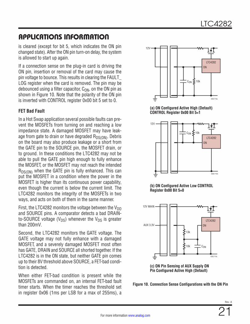
ON/OFF Control
The ON pin can be configured active high or active low with CONTROL register 0x00 bit 5 (1 for active high). In the active high configuration it is a true ON input, in the active low configuration it can be used as an ENABLE input to detect card insertion with a short pin. The delay from the ON pin commanding the part to turn on until
the GATE pins begin to rise is set by CONTROL register 0x00 bit 6. If this bit is low the GATE pins turn on immedi-ately, and if it is high they turn on after a 50ms debounce delay. Whenever the ON pin toggles, bit 4 in FAULT_LOG register 0x04 is set to indicate a change of state and the other bits in FAULT register 0x04 are reset unless the ON_FAULT_MASK bit 7 in CONTROL register 0x00 is set.
The FET_ON bit, bit 3 of CONTROL register 0x00, is set or reset by the rising and falling edges of the ON pin and by I2C write commands. When the LTC4282 comes out of UVLO the default state for bit 3 is read out of the EEPROM. If it is a 0, the part is configured to stay off after power-up and ignore the state of the ON pin. If it is a 1 the condition of the ON pin will be latched to bit 3 after the debounce period and the part will turn the GATEs on if the ON pin is in the ON state.
If the system shuts down due to a fault, it may be desir-able to restart the system simply by removing and rein-serting a load card. In cases where the LTC4282 and the switch reside on a backplane or midplane and the load resides on a plug-in card, the ON pin detects when the plug-in card is removed. Figure 10 shows an example where the ON pin is used to detect insertion. Once the plug-in card is reinserted the FAULT_LOG register 0x04
APPLICATIONS INFORMATION
Figure 9. Single MOSFET Configuration
+
VDD
P6KE16A
GATE1 GATE2
CTIMER0.18µF10ms
TIMER
LTC4282
INTVCC
CONN
ECTO
R 1
CONN
ECTO
R 2
PLUG-INBOARD
NC
4282 F09
GND
SDASCL
ALERT
R510Ω
CL
R728.7k1%R83.57k1%
VOUT12V25A
RS10.001Ω
SOURCE
FB
GPIO1GPIO2GPIO3 GP
GP
UVOVSDAISDAOSCLALERTADR0ADR1ADR2ON
SENSE2+ SENSE1+ SENSE1– SENSE2–ADC+
Q1IPB009N03L
ADC–
WP GNDCLKOUTCLKIN
Y14MHz
ABLS-4.000MHZ-B4-T
C34.7µF
C436pF
C536pF
12V
BACKPLANE
R21.18k1%
R334.0k1%
R13.4k1%
CF0.1µF25V
POWER GOOD
LTC4282
21Rev. A
For more information www.analog.com
is cleared (except for bit 5, which indicates the ON pin changed state). After the ON pin turn-on delay, the system is allowed to start up again.
If a connection sense on the plug-in card is driving the ON pin, insertion or removal of the card may cause the pin voltage to bounce. This results in clearing the FAULT_LOG register when the card is removed. The pin may be debounced using a filter capacitor, CON, on the ON pin as shown in Figure 10. Note that the polarity of the ON pin is inverted with CONTROL register 0x00 bit 5 set to 0.
FET Bad Fault
In a Hot Swap application several possible faults can pre-vent the MOSFETs from turning on and reaching a low impedance state. A damaged MOSFET may have leak-age from gate to drain or have degraded RDS(ON). Debris on the board may also produce leakage or a short from the GATE pin to the SOURCE pin, the MOSFET drain, or to ground. In these conditions the LTC4282 may not be able to pull the GATE pin high enough to fully enhance the MOSFET, or the MOSFET may not reach the intended RDS(ON) when the GATE pin is fully enhanced. This can put the MOSFET in a condition where the power in the MOSFET is higher than its continuous power capability, even though the current is below the current limit. The LTC4282 monitors the integrity of the MOSFETs in two ways, and acts on both of them in the same manner.
First, the LTC4282 monitors the voltage between the VDD and SOURCE pins. A comparator detects a bad DRAIN-to-SOURCE voltage (VDS) whenever the VDS is greater than 200mV.
Second, the LTC4282 monitors the GATE voltage. The GATE voltage may not fully enhance with a damaged MOSFET, and a severely damaged MOSFET most often has GATE, DRAIN and SOURCE all shorted together. If the LTC4282 is in the ON state, but neither GATE pin comes up to their 8V threshold above SOURCE, a FET-bad condi-tion is detected.
When either FET-bad condition is present while the MOSFETs are commanded on, an internal FET-bad fault timer starts. When the timer reaches the threshold set in register 0x06 (1ms per LSB for a max of 255ms), a
APPLICATIONS INFORMATION
Figure 10. Connection Sense Configurations with the ON Pin
4282 F10a
ON
LTC4282
12V
CON 10k
4282 F10b
12V
CON 10k
LTC4282
ON
4282 F10c
12V MAIN
AUX 3.3V
CON10k
13k
LTC4282
ON
(a) ON Configured Active High (Default) CONTROL Register 0x00 Bit 5=1
(b) ON Configured Active Low CONTROL Register 0x00 Bit 5=0
(c) ON Pin Sensing of AUX Supply ON Pin Configured Active High (Default)
LTC4282
22Rev. A
For more information www.analog.com
FET-bad fault condition is set, the part turns off, and the GATE pins are pulled low with 1mA currents. In the case of a gate-to-drain short, it may be impossible for the LTC4282 to turn off the MOSFET. In this case the LTC4282 can be configured to signal power-bad to the load so the load goes into a low current state and send a FET-bad fault alert to the controller that may be able to shut down upstream supplies and/or flag the card for service.
The LTC4282 treats a FET-bad fault similar to an overcur-rent fault, and will auto-retry after 256 timer cycles if the overcurrent auto-retry bit is set. Note that during start-up, the FET-bad condition is present because the voltage from drain to source is greater than 200mV and the GATE pins are not fully enhanced, thus the FET-bad timeout must be long enough to allow for the largest allowable load to start up. FET-bad faults are disabled by setting the FET_BAD_FAULT_TIMER value to 0x00.
FET Short Fault
A FET short fault is reported if the data converter mea-sures a current sense voltage greater than or equal to 0.25mV while the GATE pins are turned off. This condi-tion sets FET_SHORT bit 5 in STATUS register 0x1E, and FET_SHORT_FAULT bit 5 in FAULT_LOG register 0x04.
Power Bad Fault
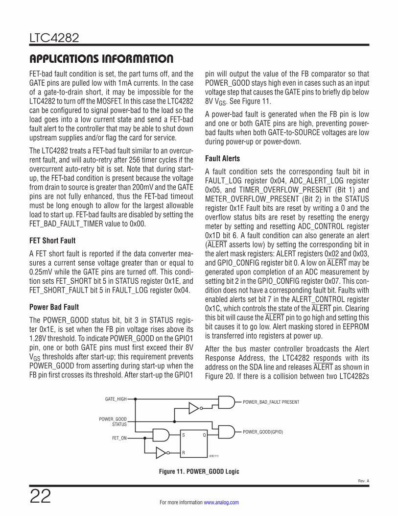
The POWER_GOOD status bit, bit 3 in STATUS regis-ter 0x1E, is set when the FB pin voltage rises above its 1.28V threshold. To indicate POWER_GOOD on the GPIO1 pin, one or both GATE pins must first exceed their 8V VGS thresholds after start-up; this requirement prevents POWER_GOOD from asserting during start-up when the FB pin first crosses its threshold. After start-up the GPIO1
pin will output the value of the FB comparator so that POWER_GOOD stays high even in cases such as an input voltage step that causes the GATE pins to briefly dip below 8V VGS. See Figure 11.
A power-bad fault is generated when the FB pin is low and one or both GATE pins are high, preventing power-bad faults when both GATE-to-SOURCE voltages are low during power-up or power-down.
Fault Alerts
A fault condition sets the corresponding fault bit in FAULT_LOG register 0x04, ADC_ALERT_LOG register 0x05, and TIMER_OVERFLOW_PRESENT (Bit 1) and METER_OVERFLOW_PRESENT (Bit 2) in the STATUS register 0x1F. Fault bits are reset by writing a 0 and the overflow status bits are reset by resetting the energy meter by setting and resetting ADC_CONTROL register 0x1D bit 6. A fault condition can also generate an alert (ALERT asserts low) by setting the corresponding bit in the alert mask registers: ALERT registers 0x02 and 0x03, and GPIO_CONFIG register bit 0. A low on ALERT may be generated upon completion of an ADC measurement by setting bit 2 in the GPIO_CONFIG register 0x07. This con-dition does not have a corresponding fault bit. Faults with enabled alerts set bit 7 in the ALERT_CONTROL register 0x1C, which controls the state of the ALERT pin. Clearing this bit will cause the ALERT pin to go high and setting this bit causes it to go low. Alert masking stored in EEPROM is transferred into registers at power up.
After the bus master controller broadcasts the Alert Response Address, the LTC4282 responds with its address on the SDA line and releases ALERT as shown in Figure 20. If there is a collision between two LTC4282s
APPLICATIONS INFORMATION
Figure 11. POWER_GOOD Logic
POWER_BAD_FAULT PRESENT
POWER_GOOD(GPIO)
POWER_GOODSTATUS
GATE_HIGH
FET_ONS
R4282 F11
Q
LTC4282
23Rev. A
For more information www.analog.com
responding with their addresses simultaneously, then the device with the lower address wins arbitration and releases its ALERT pin. The devices that lost arbitration will still hold the ALERT pin low and will respond with their addresses and release ALERT as the I2C master executes additional Alert Response protocols until ALERT is release by all devices. The ALERT pin can also be released by clearing ALERT_CONTROL bit 7 in register 0x1C with the I2C interface.
The ALERT pin can also be used as a GPIO pin, which pulls low by setting ALERT bit 6 in register 0x1C, and the ALERT pin input status is stored in STATUS register 0x1F bit 4.
Once the ALERT signal has been released from a fault, it will pull low again if the corresponding fault reoccurs, but not if the fault remains continuously present.
Resetting Faults in FAULT_LOG
The faults in FAULT_LOG register 0x04 may cause the part to latch off if their corresponding auto-retry bits are not set. In backplane resident applications it is desirable to latch off if a card has produced a failure and start up normally if the card is replaced. To allow this function the ON pin must be used as a connection sense input. When CONTROL bit 7 in register 0x00 is not set, a turn-off signal from the ON pin (card removed) will clear the FAULT_LOG register except for bit 4 (ON changed state). The entire FAULT_LOG register also cleared when the INTVCC pin falls below it’s 2.49V threshold (UVLO), and individual bits may be cleared manually via that I2C interface. Note that faults that are still present, as indicated in STATUS register 0x1E, cannot be cleared.
When the ON_FAULT_MASK bit (CONTROL bit 7 in regis-ter 0x00) is set, a turn-off signal from the ON pin will not clear the FAULT_LOG register. Additionally, when the cor-responding ON_FAULT_MASK bit is set in the EEPROM, the FAULT_LOG register 0x04 is loaded from the EEPROM (0x24) at boot. In this case, stored faults in the EEPROM are loaded into the FAULT_LOG register. This may be used in conjunction with disabling fault auto-retry to configure a card to not attempt to turn on again after a fault has been logged, even after a power cycle, until the system controller has interrogated the card and cleared the fault or flagged the card for service. For applications where the
system controller is downstream of the hot swap, all auto-retries should be enabled when the ON_FAULT_MASK bit in the EEPROM is set and fault logging is enabled so that logged faults do not permanently latch the hot swap off.
The FAULT_LOG register is not cleared when auto-retry-ing. When auto-retry is disabled the existence of a logged fault keeps the MOSFETs off. As soon as the FAULT_LOG is cleared, the MOSFETs turns on. If auto-retry is enabled, then a high STATUS bit keeps the MOSFETs off and the FAULT_LOG bit is ignored. Subsequently, when the sta-tus bit is cleared by removal of the fault condition, the MOSFETs is allowed to turn on again even though the fault bit remains set as a record of the previous fault conditions.
Reboot
The LTC4282 features a reboot command bit, located in bit 7 of ADC_CONTROL register 0x1D. Setting this bit will cause the LTC4282 to reset and copy the contents of the EEPROM to operating memory the same as after initial power up. The 50ms debounce before the part restarts is lengthened to 3.2s for reboot in order to allow load capacitance to discharge and reset before the LTC4282 turns back on. On systems where the Hot Swap controller supplies power to the I2C master, this allows the master to issue a command that power cycles the entire board, including itself.
Data Converters
The LTC4282 incorporates a pair of sigma delta A/D con-verters that are configurable to 12 or 16 bits. One converter continuously samples the current sense voltage, while the other monitors the input/output voltage and the voltage on a GPIO input. The sigma-delta architecture inherently aver-ages signal noise during the measurement period.
The data converters may be run in a 12-bit or 16-bit mode, as selected by bit 1 in ILIM_ADJUST register 0x11. The second data converter may be configured to measure VIN at the VDD pin or VOUT at the SOURCE pin by setting bit 3, and can select between measuring GPIO2 or GPIO3 with bit 2. The data converter full scale is 40mV for the cur-rent sense voltage, a choice of 33.28V, 16.64V, 8.32V or 5.547V for VDD and VSOURCE, and 1.28V for GPIO.
APPLICATIONS INFORMATION
LTC4282
24Rev. A
For more information www.analog.com
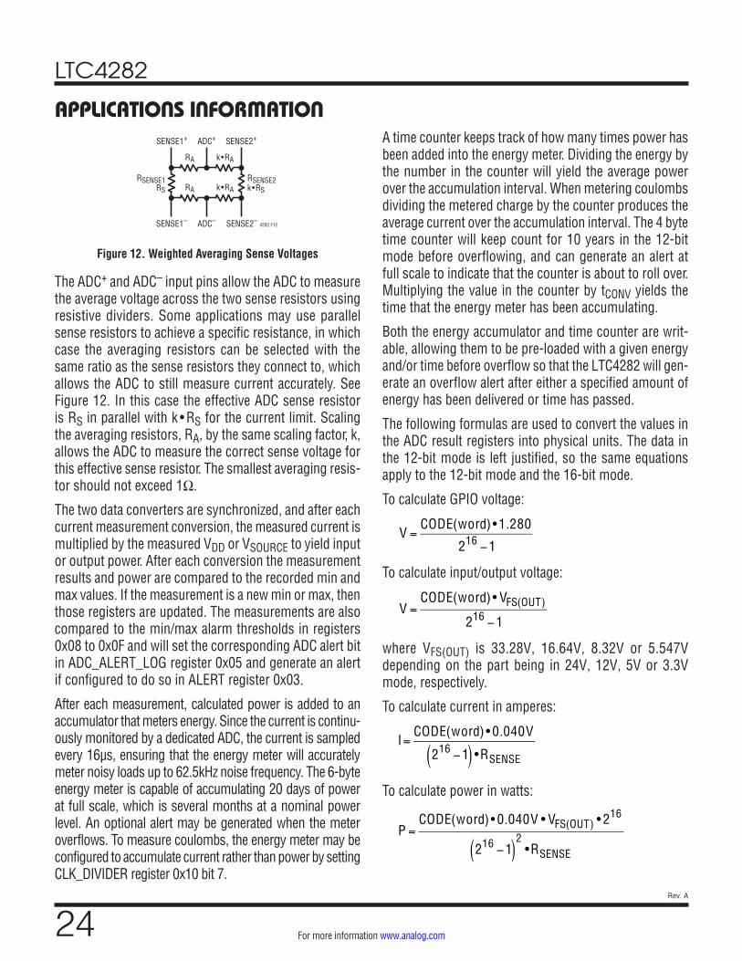
The ADC+ and ADC– input pins allow the ADC to measure the average voltage across the two sense resistors using resistive dividers. Some applications may use parallel sense resistors to achieve a specific resistance, in which case the averaging resistors can be selected with the same ratio as the sense resistors they connect to, which allows the ADC to still measure current accurately. See Figure 12. In this case the effective ADC sense resistor is RS in parallel with k • RS for the current limit. Scaling the averaging resistors, RA, by the same scaling factor, k, allows the ADC to measure the correct sense voltage for this effective sense resistor. The smallest averaging resis-tor should not exceed 1Ω.
The two data converters are synchronized, and after each current measurement conversion, the measured current is multiplied by the measured VDD or VSOURCE to yield input or output power. After each conversion the measurement results and power are compared to the recorded min and max values. If the measurement is a new min or max, then those registers are updated. The measurements are also compared to the min/max alarm thresholds in registers 0x08 to 0x0F and will set the corresponding ADC alert bit in ADC_ALERT_LOG register 0x05 and generate an alert if configured to do so in ALERT register 0x03.
After each measurement, calculated power is added to an accumulator that meters energy. Since the current is continu-ously monitored by a dedicated ADC, the current is sampled every 16µs, ensuring that the energy meter will accurately meter noisy loads up to 62.5kHz noise frequency. The 6-byte energy meter is capable of accumulating 20 days of power at full scale, which is several months at a nominal power level. An optional alert may be generated when the meter overflows. To measure coulombs, the energy meter may be configured to accumulate current rather than power by setting CLK_DIVIDER register 0x10 bit 7.
A time counter keeps track of how many times power has been added into the energy meter. Dividing the energy by the number in the counter will yield the average power over the accumulation interval. When metering coulombs dividing the metered charge by the counter produces the average current over the accumulation interval. The 4 byte time counter will keep count for 10 years in the 12-bit mode before overflowing, and can generate an alert at full scale to indicate that the counter is about to roll over. Multiplying the value in the counter by tCONV yields the time that the energy meter has been accumulating.
Both the energy accumulator and time counter are writ-able, allowing them to be pre-loaded with a given energy and/or time before overflow so that the LTC4282 will gen-erate an overflow alert after either a specified amount of energy has been delivered or time has passed.
The following formulas are used to convert the values in the ADC result registers into physical units. The data in the 12-bit mode is left justified, so the same equations apply to the 12-bit mode and the 16-bit mode.
To calculate GPIO voltage:
V =
CODE(word) •1.280
216 −1
To calculate input/output voltage:
V =
CODE(word) • VFS(OUT)
216 −1
where VFS(OUT) is 33.28V, 16.64V, 8.32V or 5.547V depending on the part being in 24V, 12V, 5V or 3.3V mode, respectively.
To calculate current in amperes:
I=CODE(word) • 0.040V
216 −1( ) •RSENSE
To calculate power in watts:
P =CODE(word) • 0.040V • VFS(OUT) • 216
216 −1( )2
•RSENSE
APPLICATIONS INFORMATION
Figure 12. Weighted Averaging Sense Voltages
RSENSE2k•RS
4282 F12
RSENSE1RS
k•RA
ADC+
ADC–
SENSE1+ SENSE2+
SENSE1– SENSE2–
k•RA
RA
RA
LTC4282
25Rev. A
For more information www.analog.com
To calculate energy in joules:
E =CODE(48 bits) • 0.040V • VFS(OUT) • tCONV • 28
216 −1( )2
•RSENSE
To calculate coulombs:
C =
CODE(48 Bits) • 0.040V • tCONV
(216 −1) •RSENSE
where tCONV = (1/fCONV) is 0.065535s for 12-bit mode and 1.0486s for 16-bit mode.
To calculate average power over the energy accumulation period:
P(AVG)=
EtCONV •CODE(COUNTER)
To calculate Average current:
I(AVG)=
CtCONV •CODE(COUNTER)
To calculate GPIO voltage Alarm thresholds:
V =
CODE(byte) •1.280255
To calculate input/output voltage Alarm thresholds:
VALARM =
CODE(byte) • VFS(OUT)
255
where VFS(OUT) is 33.28V, 16.64V, 8.32V or 5.547V depending on the part being in 24V, 12V, 5V or 3.3V mode, respectively.
To calculate current Alarm thresholds in amps:
I=
CODE(byte) • 0.040V255 •RSENSE
To calculate power Alarm threshold in watts:
P =
CODE(byte) • 0.040V • VFS(OUT) • 28
RSENSE • 255 • 255
Note that falling Alarm thresholds use CODE(byte)+1 in the above equations since they trip at the top edge of the code, which is 1LSB higher than the rising threshold.
Crystal Oscillator/External Clock
Accurately measuring energy by integrating power requires a precise integration period. The on-chip clock of the LTC4282 is trimmed to 1.5% and specified (fCONV) over temperature to 5% and is invoked by grounding CLKIN. For increased accuracy a crystal oscillator or external precision clock may be used on the CLKIN and CLKOUT pins. A 4MHz crystal oscillator or resonator may be connected to the two CLK pins as shown in Figure 1.
Crystal oscillators are sensitive to noise and parasitic capacitance. Care should be taken in layout to minimize trace length between the LTC4282 and the crystal. Keep noisy traces away from the crystal traces, or shield the crystal traces with a ground trace.
Alternatively, an external clock may be applied to CLKIN with CLKOUT left unconnected. The LTC4282 can accept an external clock between 250kHz and 15.5MHz, with clocks faster than 250kHz reduced to 250kHz by a pro-grammable divider, the clock frequency is divided by twice the value in register 0x10 bits 0-4. Code 00000 passes the clock through CLK_DIVIDER without division. Write code 01000 divides a 4MHz clock down to 250kHz. The divided external clock may differ from 250kHz by 5% without affecting other specifications.
Configuring the GPIO Pins
The LTC4282 has three GPIO pins and an ALERT pin, all of which can be used as general purpose input/output pins. The GPIO1 pin is configured using the GPIO_CONFIG register 0x07 bits 5-4. GPIO2 will pull low to indicate MOSFET stress if GPIO_CONFIG bit 1 is set and pulls low if bit 6 is low. GPIO3 pulls low if GPIO_CONFIG bit 7 is set and is otherwise high impedance. The ALERT pin can be used as a GPIO pin by setting all the alert enable bits to 0 to disable alerts, then setting bit 6 in ALERT_CONTROL register 0x1C. Bit 7 in ALERT_CONTROL can also be set to pull the ALERT pin low, but bit 7 will cause the part to respond to the alert response protocol, while bit 6 will not.
APPLICATIONS INFORMATION
LTC4282
26Rev. A
For more information www.analog.com
GPIO1-GPIO3 and ALERT all have comparators monitoring the voltage on these pins with a threshold of 1.28V even when the pins are configured as outputs. The results may be read from the second byte of the STATUS register, 0x1F, bits 4-7.
Supply Transients
In card-resident applications, output short circuits work-ing against the inductive nature of the supply can easily cause the input voltage to dip below the UV threshold.
In severe cases where the supply inductance is 500nH or more, the input can dip below the VDD undervoltage lockout threshold of 2.66V. Because the current passing through the sense resistor changes no faster than a rate of VSUPPLY/LSUPPLY, such as 12V/500nH = 24A/µs, it is pos-sible for the UV comparator and in particular, the VDD UVLO circuit to respond before the current reaches the current limit threshold. The VDD UVLO circuit responds after a 2µs filter delay, pulling the GATE pins to SOURCE with 600mA. Once the MOSFET turns off, VDD will return to its nominal voltage and the part initiates a new startup sequence. The UV comparator responds after a 15µs filter delay, making it less likely that this path will engage before current limiting commences; adding a 100nF filter capacitor to the UV pin ensures this. The fast current limit amplifier engages at 3x the current limit threshold, and has a propagation delay of 500ns. If the supply inductance is less than 500nH in a 12V application, it is unlikely that the VDD UVLO threshold will be breached and the fast di/dt rate allows the current to rise to the 3x level long before the UV pin responds.
Once the fast current limit amplifier begins to arrest the short circuit current, the input voltage rapidly recovers and even overshoots its DC value. The LTC4282 is safe from damage up to 45V. To minimize spikes in backplane-resident applications, bypass the LTC4282 input supply with an electrolytic capacitor between VDD and GND. In card-resident applications clamp the VDD pin with a surge suppressor Z1, as shown in Figure 1.
The worst-case Z1 current is that which triggers the fast current limit circuit. Several 1500W surge suppressors may be required to clamp this current for high power applications. Many 20V to 30V MOSFETs enter avalanche breakdown before 45V. In those cases the MOSFET can act as a surge suppressor and protect the Hot Swap
controller from inductive input voltage surges. In appli-cations where a high current ground is not available to connect the surge suppressor, the surge suppressor may be connected from input to output, allowing the output capacitance to absorb spikes.
Design Example
As a design example, consider the following specifications: VIN = 12V, IMAX = 100A, CL = 3300μF, VUV(ON) = 10.75V, VOV(OFF) = 14.0V, VPWRGD(UP) = 11.6V, and I2C address = 1010011, using two parallel MOSFETs with current limit set at 25mV. This completed design is shown in Figure 13.
Selection of the sense resistors, RS1/RS2, is set by the current limit threshold of 25mV:
RS =
25mV • 2ResistorsIMAX
= 0.5mΩ
Each sensor resistor may need to be divided into several parallel sense resistors in order to keep the power dis-sipation within limits. Often the temperature coefficient of current sense resistors is poor for very low values, in which cases accuracy is improved by using several larger value resistors in parallel instead of a single low value resistor. The same resistor averaging method used for the ADC pins in Figure 12 may be used with the SENSE pins to accurately sense the current in parallel resistors.
The MOSFETs are sized to handle the power dissipa-tion during inrush when output capacitor COUT is being charged.
A method to determine power dissipation during inrush is based on the principle that:
Energy in CL = Energy in Q1 and Q2
where:
Energy in CL =
12
CV2 =12
3.3mF( ) 12V( )2= 0.24J
During inrush, current limit foldback will limit the power dissipation in each MOSFET to:
PDISS =
7.5mV •12VRS
= 180W
APPLICATIONS INFORMATION
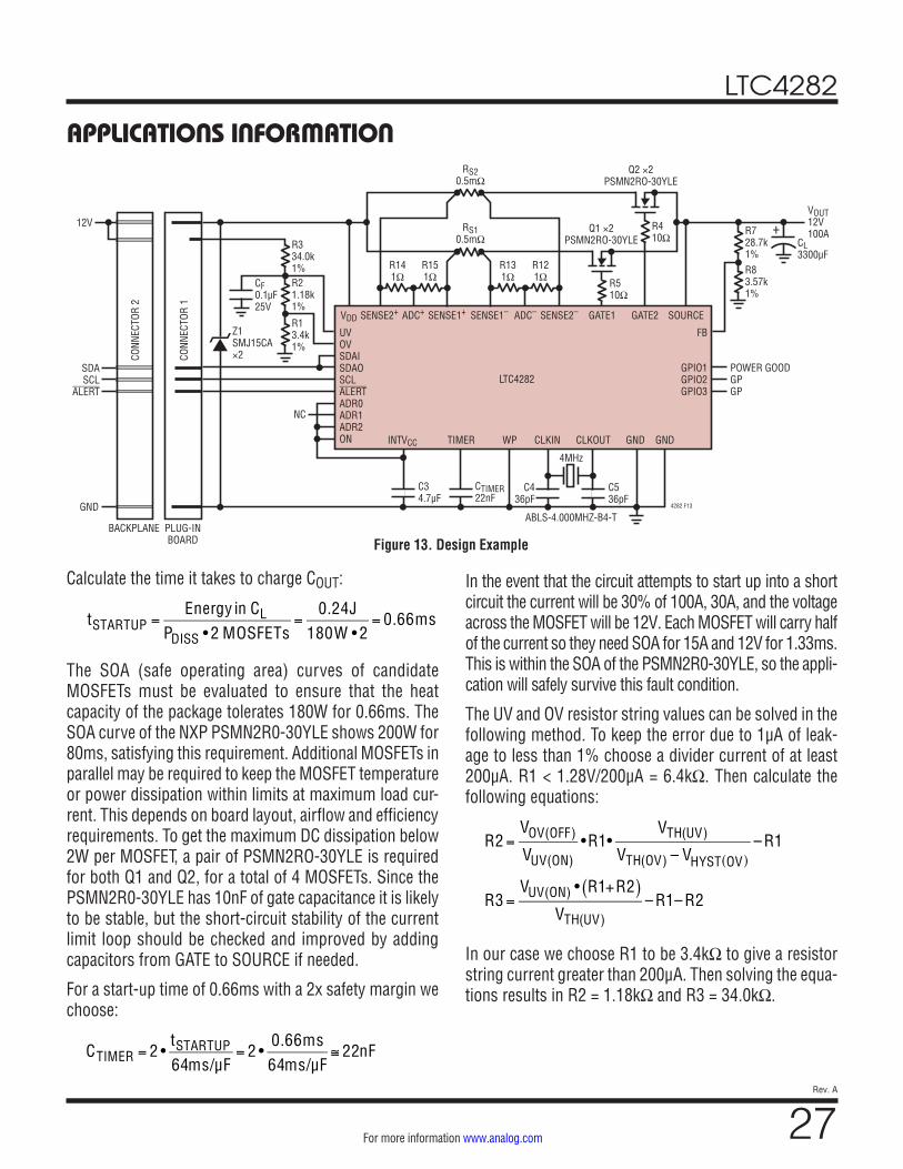
LTC4282
27Rev. A
For more information www.analog.com
Calculate the time it takes to charge COUT:
tSTARTUP =
Energy in CLPDISS • 2 MOSFETs
=0.24J
180W • 2= 0.66ms
The SOA (safe operating area) curves of candidate MOSFETs must be evaluated to ensure that the heat capacity of the package tolerates 180W for 0.66ms. The SOA curve of the NXP PSMN2R0-30YLE shows 200W for 80ms, satisfying this requirement. Additional MOSFETs in parallel may be required to keep the MOSFET temperature or power dissipation within limits at maximum load cur-rent. This depends on board layout, airflow and efficiency requirements. To get the maximum DC dissipation below 2W per MOSFET, a pair of PSMN2RO-30YLE is required for both Q1 and Q2, for a total of 4 MOSFETs. Since the PSMN2R0-30YLE has 10nF of gate capacitance it is likely to be stable, but the short-circuit stability of the current limit loop should be checked and improved by adding capacitors from GATE to SOURCE if needed.
For a start-up time of 0.66ms with a 2x safety margin we choose:
CTIMER = 2 •
tSTARTUP64ms/µF
= 2 •0.66ms64ms/µF
≅ 22nF
In the event that the circuit attempts to start up into a short circuit the current will be 30% of 100A, 30A, and the voltage across the MOSFET will be 12V. Each MOSFET will carry half of the current so they need SOA for 15A and 12V for 1.33ms. This is within the SOA of the PSMN2R0-30YLE, so the appli-cation will safely survive this fault condition.
The UV and OV resistor string values can be solved in the following method. To keep the error due to 1µA of leak-age to less than 1% choose a divider current of at least 200µA. R1 < 1.28V/200µA = 6.4kΩ. Then calculate the following equations:
R2 =VOV(OFF)
VUV(ON)•R1•
VTH(UV)
VTH(OV) – VHYST OV( )– R1
R3 =VUV(ON) • R1+R2( )
VTH(UV)– R1– R2
In our case we choose R1 to be 3.4kΩ to give a resistor string current greater than 200μA. Then solving the equa-tions results in R2 = 1.18kΩ and R3 = 34.0kΩ.
APPLICATIONS INFORMATION
+
VDDZ1SMJ15CA×2
GATE1 GATE2
CTIMER22nF
TIMER
LTC4282
INTVCC
CONN
ECTO
R 1
CONN
ECTO
R 2
PLUG-INBOARD
NC
4282 F13GND
SDASCL
ALERT
R510Ω
CL3300µF
R410Ω
R728.7k1%R83.57k1%
VOUT12V100A
RS20.5mΩ
RS10.5mΩ
SOURCE
FB
GPIO1GPIO2GPIO3
POWER GOODGPGP
UVOVSDAISDAOSCLALERTADR0ADR1ADR2ON
SENSE2+ SENSE1+ SENSE1– SENSE2–ADC+
R141Ω
R151Ω
R131Ω
R121Ω
Q1 ×2PSMN2RO-30YLE
Q2 ×2PSMN2RO-30YLE
ADC–
WP GND GNDCLKOUTCLKIN
4MHz
ABLS-4.000MHZ-B4-T
C34.7µF
C436pF
C536pF
12V
BACKPLANE
R21.18k1%
R334.0k1%
R13.4k1%
CF0.1µF25V
Figure 13. Design Example
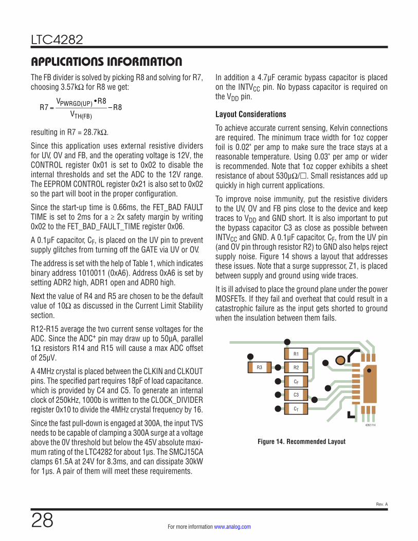
LTC4282
28Rev. A
For more information www.analog.com
The FB divider is solved by picking R8 and solving for R7, choosing 3.57kΩ for R8 we get:
R7 =
VPWRGD(UP) •R8
VTH(FB)– R8
resulting in R7 = 28.7kΩ.
Since this application uses external resistive dividers for UV, OV and FB, and the operating voltage is 12V, the CONTROL register 0x01 is set to 0x02 to disable the internal thresholds and set the ADC to the 12V range. The EEPROM CONTROL register 0x21 is also set to 0x02 so the part will boot in the proper configuration.
Since the start-up time is 0.66ms, the FET_BAD FAULT TIME is set to 2ms for a ≥ 2x safety margin by writing 0x02 to the FET_BAD_FAULT_TIME register 0x06.
A 0.1μF capacitor, CF, is placed on the UV pin to prevent supply glitches from turning off the GATE via UV or OV.
The address is set with the help of Table 1, which indicates binary address 1010011 (0xA6). Address 0xA6 is set by setting ADR2 high, ADR1 open and ADR0 high.
Next the value of R4 and R5 are chosen to be the default value of 10Ω as discussed in the Current Limit Stability section.
R12-R15 average the two current sense voltages for the ADC. Since the ADC+ pin may draw up to 50µA, parallel 1Ω resistors R14 and R15 will cause a max ADC offset of 25µV.
A 4MHz crystal is placed between the CLKIN and CLKOUT pins. The specified part requires 18pF of load capacitance. which is provided by C4 and C5. To generate an internal clock of 250kHz, 1000b is written to the CLOCK_DIVIDER register 0x10 to divide the 4MHz crystal frequency by 16.
Since the fast pull-down is engaged at 300A, the input TVS needs to be capable of clamping a 300A surge at a voltage above the 0V threshold but below the 45V absolute maxi-mum rating of the LTC4282 for about 1µs. The SMCJ15CA clamps 61.5A at 24V for 8.3ms, and can dissipate 30kW for 1µs. A pair of them will meet these requirements.
APPLICATIONS INFORMATIONIn addition a 4.7μF ceramic bypass capacitor is placed on the INTVCC pin. No bypass capacitor is required on the VDD pin.
Layout Considerations
To achieve accurate current sensing, Kelvin connections are required. The minimum trace width for 1oz copper foil is 0.02" per amp to make sure the trace stays at a reasonable temperature. Using 0.03" per amp or wider is recommended. Note that 1oz copper exhibits a sheet resistance of about 530μΩ/£. Small resistances add up quickly in high current applications.
To improve noise immunity, put the resistive dividers to the UV, OV and FB pins close to the device and keep traces to VDD and GND short. It is also important to put the bypass capacitor C3 as close as possible between INTVCC and GND. A 0.1μF capacitor, CF, from the UV pin (and OV pin through resistor R2) to GND also helps reject supply noise. Figure 14 shows a layout that addresses these issues. Note that a surge suppressor, Z1, is placed between supply and ground using wide traces.
It is ill advised to place the ground plane under the power MOSFETs. If they fail and overheat that could result in a catastrophic failure as the input gets shorted to ground when the insulation between them fails.
R1
R3 R2
CF
CT
4282 F14
C3
Figure 14. Recommended Layout
LTC4282
29Rev. A
For more information www.analog.com
APPLICATIONS INFORMATIONDigital Interface
The LTC4282 communicates with a bus master using a 2-wire interface compatible with I2C Bus and SMBus, an I2C extension for low power devices. The LTC4282 is a read-write slave device and supports SMBus bus Read Byte, Write Byte, Read Word and Write Word commands, as well as I2C continuous read and continuous write com-mands. Data formats for these commands are shown in Figure 15 through Figure 22.
START and STOP Conditions
When the bus is idle, both SCL and SDA are high. A bus master signals the beginning of a transmission with a START condition by transitioning SDA from high to low while SCL is high, as shown in Figure 15. When the master has finished communicating with the slave, it issues a STOP condition by transitioning SDA from low to high while SCL is high. The bus is then free for another transmission.
I2C Device Addressing
Twenty-seven distinct bus addresses are available using three 3-state address pins, ADR0-ADR2. Table 1 shows the correspondence between pin states and addresses. Note that address bits 7 and 6 are internally configured to 10. In addition, the LTC4282 responds to two spe-cial addresses. Address 0xBE is a mass write address that writes to all LTC4282s, regardless of their individual address settings. Mass write can be disabled by setting bit 4 in CONTROL register 0x00 to zero. Address (0x19) is the SMBus Alert Response Address. If the LTC4282 is pulling low on the ALERT pin, it acknowledges this address by broadcasting its address and releasing the ALERT pin.
Acknowledge
The acknowledge signal is used in handshaking between transmitter and receiver to indicate that the last byte of data was received. The transmitter always releases the SDA line during the acknowledge clock pulse. When the slave is the receiver, it pulls down the SDA line so that it remains LOW during this pulse to acknowledge receipt
of the data. If the slave fails to acknowledge by leaving SDA high, then the master may abort the transmission by generating a STOP condition. When the master is receiv-ing data from the slave, the master pulls down the SDA line during the clock pulse to indicate receipt of the data. After the last byte has been received the master leaves the SDA line HIGH (not acknowledge) and issues a stop condition to terminate the transmission.
Write Protocol
The master begins communication with a START condi-tion followed by the seven bit slave address and the R/W bit set to zero, as shown in Figure 16. The addressed LTC4282 acknowledges this and then the master sends a command byte indicating which internal register the mas-ter wishes to write. The LTC4282 acknowledges this and then latches the command byte into its internal Register Address pointer. The master then delivers the data byte and the LTC4282 acknowledges once more and writes the data to the destination register specified by the Register Address pointer, then the pointer is incremented. If the Master sends additional bytes, they are written sequen-tially to the registers in order of their binary addresses. The transmission is ended when the master sends a STOP condition.
Read Protocol
The master begins a read operation with a START condi-tion followed by the seven bit slave address and the R/W bit set to zero, as shown in Figure 19. The addressed LTC4282 acknowledges this and then the master sends a command byte which indicates which internal register the master wishes to read. The LTC4282 acknowledges this and then latches the command byte into its inter-nal Register Address pointer. The master then sends a repeated START condition followed by the same seven bit address with the R/W bit now set to one. The LTC4282 acknowledges and send the contents of the requested reg-ister. As long as the master acknowledges the transmitted data byte the internal Register Address pointer is incre-mented and the next register byte is sent. The transmis-sion is ended when the master sends a STOP condition.
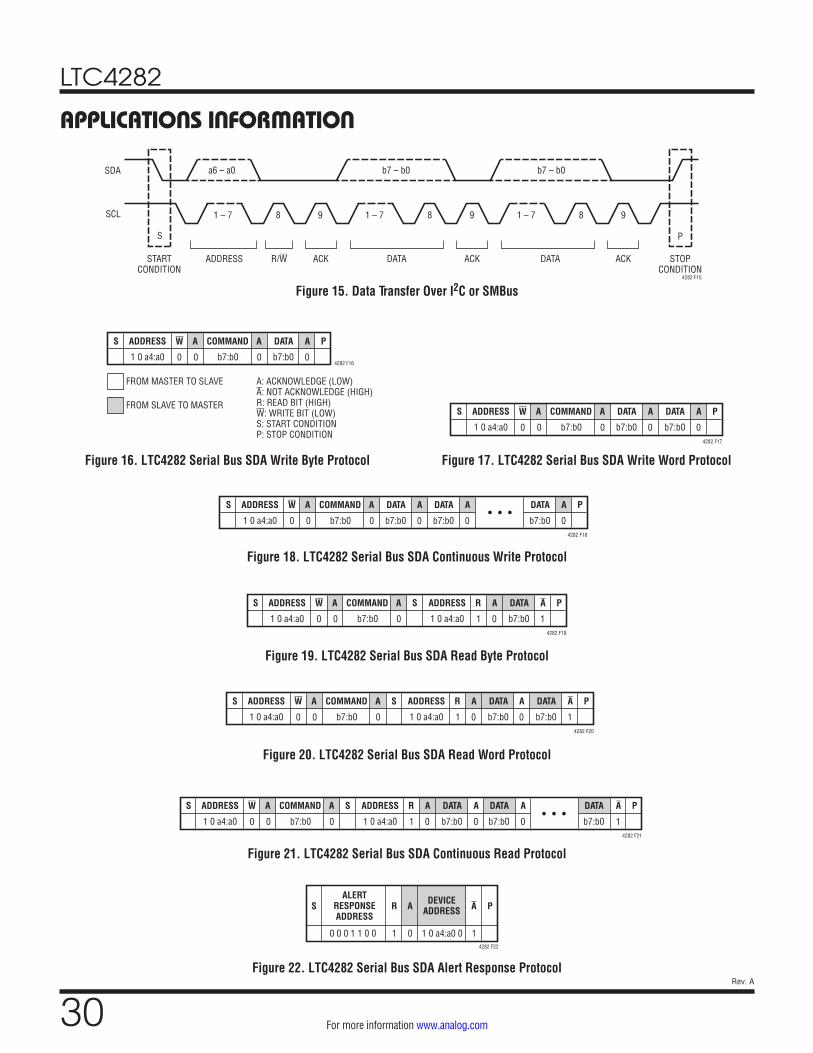
LTC4282
30Rev. A
For more information www.analog.com
APPLICATIONS INFORMATION
a6 – a0 b7 – b0 b7 – b0
9
ACK
4282 F15
ACKACKADDRESSSTARTCONDITION
STOPCONDITION
R/W DATADATA
89898
S
SDA
SCL 1 – 71 – 71 – 7
P
Figure 15. Data Transfer Over I2C or SMBus
ADDRESS
1 0 a4:a0
FROM MASTER TO SLAVE A: ACKNOWLEDGE (LOW)A: NOT ACKNOWLEDGE (HIGH)R: READ BIT (HIGH)W: WRITE BIT (LOW)S: START CONDITIONP: STOP CONDITION
FROM SLAVE TO MASTER
b7:b0 b7:b04282 F16
COMMAND DATAS
0 0 0 0
A A A PW
Figure 16. LTC4282 Serial Bus SDA Write Byte Protocol Figure 17. LTC4282 Serial Bus SDA Write Word Protocol
Figure 18. LTC4282 Serial Bus SDA Continuous Write Protocol
Figure 19. LTC4282 Serial Bus SDA Read Byte Protocol
Figure 20. LTC4282 Serial Bus SDA Read Word Protocol
Figure 21. LTC4282 Serial Bus SDA Continuous Read Protocol
Figure 22. LTC4282 Serial Bus SDA Alert Response Protocol
ADDRESS
1 0 a4:a0 b7:b0 b7:b04282 F17
COMMAND DATAS
0 0 0 0
A A A
b7:b0
DATA
0
A PW
ADDRESS
1 0 a4:a0 b7:b0 b7:b04282 F18
COMMAND DATAS
0 0 0 0
A A A
b7:b0
DATA
0
A PW• • •
b7:b0
DATA
0
A
ADDRESS
1 0 a4:a0
ADDRESS
1 0 a4:a0b7:b0 b7:b04282 F19
COMMAND DATAS S R
0 0 0 1
A A A
01
A PW
ADDRESS
1 0 a4:a0
ADDRESS
1 0 a4:a0b7:b0 b7:b04282 F20
COMMAND DATAS S R
0 0 0 1
A A A
01
A PW
b7:b0
DATA
0
A
ADDRESS
1 0 a4:a0
ADDRESS
1 0 a4:a0b7:b0 b7:b04282 F21
COMMAND DATA
b7:b0
DATAS S R
0 0 0 1
A A A
01
A
0
A
b7:b0
DATA
0
A PW• • •
ALERTRESPONSEADDRESS
DEVICEADDRESS
0 0 0 1 1 0 0
S R
1 14282 F22
A PA
0 1 0 a4:a0 0
LTC4282
31Rev. A
For more information www.analog.com
APPLICATIONS INFORMATIONData Synchronization
The ADC measurements and subsequent computed val-ues are 16-48 bits wide, but must be read over I2C in 8-bit segments. To ensure that the words are not updated in the middle of reading them, the LTC4282 latches these results while the I2C interface is busy. As long as the ADC data is read out in a single transaction, all the data will be synchronized. A STOP condition frees the LTC4282 to update the ADC result registers. Status and fault registers are updated in real time.
Alert Response Protocol
When any of the fault bits in FAULT_LOG register 0x04 are set, an optional bus alert is generated if the appropri-ate bit in the ALERT register 0x02 is also set. If an alert is enabled, the corresponding fault causes the ALERT pin to pull low. After the bus master controller broadcasts the Alert Response Address, the LTC4282 responds with its address on the SDA line and then releases ALERT when it has successfully completed transmitting its address as shown in Figure 22.
The ALERT signal is not pulled low again until the FAULT register 0x04 indicates a different fault as occurred or the original fault is cleared and it occurs again. Note that this means repeated or continuing faults do not generate alerts until the associated FAULT_LOG register bit has been cleared.
EEPROM
The LTC4282 has an onboard EEPROM to allow nonvola-tile configuration and fault logging. The EEPROM regis-ters are denoted by ‘EE’ in the first column of register Table 2. The EEPROM registers may be read and writ-ten like any other register except that the EEPROM takes about 2ms to write data. While the EEPROM is writing, the EEPROM_BUSY bit, bit 2 in STATUS register 0x1F is set to 1. While the EEPROM is busy the I2C interface will NACK commands to read or write to EEPROM registers, but other registers may be accessed during this time. When the EEPROM finishes writing, the EEPROM_BUSY bit will reset and the EEPROM_DONE bit, bit 7 in FAULT_LOG register 0x04 will be set. If configured to generate an alert
on EEPROM_DONE, Bit 7 in ALERT register 0x02, the ALERT pin will pull low to alert the host that the EEPROM write has finished and the LTC4282 EEPROM is ready to receive another byte.
When the LTC4282 comes out of UVLO or receives a REBOOT command the contents of the EEPROM are cop-ied to the corresponding operating registers, which are offset from the EEPROM register addresses by 0x20. The SCRATCH_PAD registers, 0x4C-0x4F, are free for general purpose use, such as storing fault history, serial numbers or calibration data. The factory default EEPROM contents will make the LTC4282 behave similar to the LTC4215 to ease design migration and provide a useful design start-ing point.
The ADC_ALERT_LOG register(0x05) is not loaded from the EEPROM at boot, and the FAULT_LOG register (0x04) is only loaded at boot if the ON_FAULT_MASK bit is set in the EEPROM (bit 7, register 0x20). The register data is copied into the EEPROM when any of the bits in the log registers transition high and fault logging is enabled in ADC_CONTROL register 0x1D. Fault logging is disabled by default after boot so that logged faults are not inad-vertently cleared by powering up with a fault condition and overwriting the EEPROM. A 4.7µF capacitor on the INTVCC pin allows the LTC4282 to operate and log faults to the EEPROM if input power is lost. A 1µF capacitor may be used in applications that do not require EEPROM fault logging.
The WP pin prevents I2C writes to the EEPROM when high. Attempts to write to the EEPROM while WP is high will result in a NACK and no action. Usually the WP pin is tied high through a resistor with a probe pad to allow it to be pulled low manually; it may also be tied low to enable writes all the time or connected to a GPIO pin or other logic-level signal to allow software control of WP. The EEPROM may still be read when WP is high. The FAULT_LOG and ADC_ALERT_LOG registers of the EEPROM will still log faults when the WP pin is high. LTC can provide programmed parts may which have WP locked in a high state to make it impossible to change the default configuration by any means. Please contact the factory.
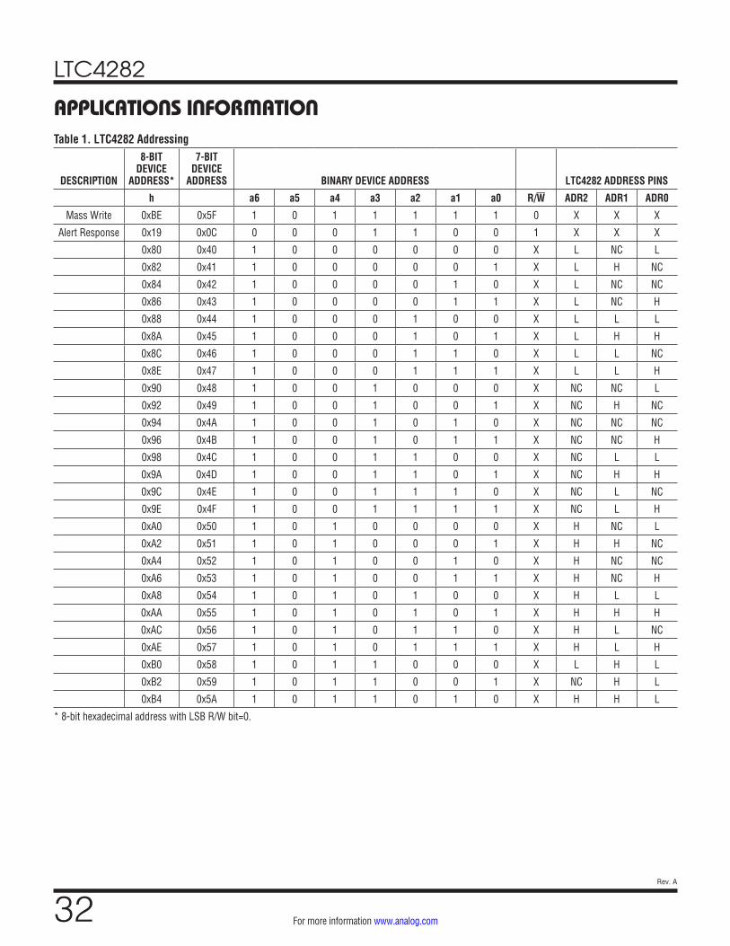
LTC4282
32Rev. A
For more information www.analog.com
APPLICATIONS INFORMATIONTable 1. LTC4282 Addressing
DESCRIPTION
8-BIT DEVICE
ADDRESS*
7-BIT DEVICE
ADDRESS BINARY DEVICE ADDRESS LTC4282 ADDRESS PINS
h a6 a5 a4 a3 a2 a1 a0 R/W ADR2 ADR1 ADR0
Mass Write 0xBE 0x5F 1 0 1 1 1 1 1 0 X X X
Alert Response 0x19 0x0C 0 0 0 1 1 0 0 1 X X X
0x80 0x40 1 0 0 0 0 0 0 X L NC L
0x82 0x41 1 0 0 0 0 0 1 X L H NC
0x84 0x42 1 0 0 0 0 1 0 X L NC NC
0x86 0x43 1 0 0 0 0 1 1 X L NC H
0x88 0x44 1 0 0 0 1 0 0 X L L L
0x8A 0x45 1 0 0 0 1 0 1 X L H H
0x8C 0x46 1 0 0 0 1 1 0 X L L NC
0x8E 0x47 1 0 0 0 1 1 1 X L L H
0x90 0x48 1 0 0 1 0 0 0 X NC NC L
0x92 0x49 1 0 0 1 0 0 1 X NC H NC
0x94 0x4A 1 0 0 1 0 1 0 X NC NC NC
0x96 0x4B 1 0 0 1 0 1 1 X NC NC H
0x98 0x4C 1 0 0 1 1 0 0 X NC L L
0x9A 0x4D 1 0 0 1 1 0 1 X NC H H
0x9C 0x4E 1 0 0 1 1 1 0 X NC L NC
0x9E 0x4F 1 0 0 1 1 1 1 X NC L H
0xA0 0x50 1 0 1 0 0 0 0 X H NC L
0xA2 0x51 1 0 1 0 0 0 1 X H H NC
0xA4 0x52 1 0 1 0 0 1 0 X H NC NC
0xA6 0x53 1 0 1 0 0 1 1 X H NC H
0xA8 0x54 1 0 1 0 1 0 0 X H L L
0xAA 0x55 1 0 1 0 1 0 1 X H H H
0xAC 0x56 1 0 1 0 1 1 0 X H L NC
0xAE 0x57 1 0 1 0 1 1 1 X H L H
0xB0 0x58 1 0 1 1 0 0 0 X L H L
0xB2 0x59 1 0 1 1 0 0 1 X NC H L
0xB4 0x5A 1 0 1 1 0 1 0 X H H L
* 8-bit hexadecimal address with LSB R/W bit=0.
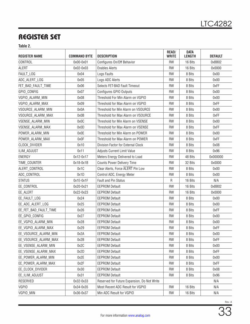
LTC4282
33Rev. A
For more information www.analog.com
REGISTER SETTable 2.
REGISTER NAME COMMAND BYTE DESCRIPTIONREAD/WRITE
DATA LENGTH DEFAULT
CONTROL 0x00-0x01 Configures On/Off Behavior RW 16 Bits 0xBB02
ALERT 0x02-0x03 Enables Alerts RW 16 Bits 0x0000
FAULT_LOG 0x04 Logs Faults RW 8 Bits 0x00
ADC_ALERT_LOG 0x05 Logs ADC Alerts RW 8 Bits 0x00
FET_BAD_FAULT_TIME 0x06 Selects FET-BAD Fault Timeout RW 8 Bits 0xFF
GPIO_CONFIG 0x07 Configures GPIO Outputs RW 8 Bits 0x00
VGPIO_ALARM_MIN 0x08 Threshold For Min Alarm on VGPIO RW 8 Bits 0x00
VGPIO_ALARM_MAX 0x09 Threshold for Max Alarm on VGPIO RW 8 Bits 0xFF
VSOURCE_ALARM_MIN 0x0A Threshold for Min Alarm on VSOURCE RW 8 Bits 0x00
VSOURCE_ALARM_MAX 0x0B Threshold for Max Alarm on VSOURCE RW 8 Bits 0xFF
VSENSE_ALARM_MIN 0x0C Threshold for Min Alarm on VSENSE RW 8 Bits 0x00
VSENSE_ALARM_MAX 0x0D Threshold for Max Alarm on VSENSE RW 8 Bits 0xFF
POWER_ALARM_MIN 0x0E Threshold for Min Alarm on POWER RW 8 Bits 0x00
POWER_ALARM_MAX 0x0F Threshold for Max Alarm on POWER RW 8 Bits 0xFF
CLOCK_DIVIDER 0x10 Division Factor for External Clock RW 8 Bits 0x08
ILIM_ADJUST 0x11 Adjusts Current Limit Value RW 8 Bits 0x96
ENERGY 0x12-0x17 Meters Energy Delivered to Load RW 48 Bits 0x000000
TIME_COUNTER 0x18-0x1B Counts Power Delivery Time RW 32 Bits 0x0000
ALERT_CONTROL 0x1C Clear Alerts, Force ALERT Pin Low RW 8 Bits 0x00
ADC_CONTROL 0x1D Control ADC, Energy Meter RW 8 Bits 0x00
STATUS 0x1E-0x1F Fault and Pin Status R 16 Bits N/A
EE_CONTROL 0x20-0x21 EEPROM Default RW 16 Bits 0xBB02
EE_ALERT 0x22-0x23 EEPROM Default RW 16 Bits 0x0000
EE_FAULT_LOG 0x24 EEPROM Default RW 8 Bits 0x00
EE_ADC_ALERT_LOG 0x25 EEPROM Default RW 8 Bits 0x00
EE_FET_BAD_FAULT_TIME 0x26 EEPROM Default RW 8 Bits 0xFF
EE_GPIO_CONFIG 0x27 EEPROM Default RW 8 Bits 0x00
EE_VGPIO_ALARM_MIN 0x28 EEPROM Default RW 8 Bits 0x00
EE_VGPIO_ALARM_MAX 0x29 EEPROM Default RW 8 Bits 0xFF
EE_VSOURCE_ALARM_MIN 0x2A EEPROM Default RW 8 Bits 0x00
EE_VSOURCE_ALARM_MAX 0x2B EEPROM Default RW 8 Bits 0xFF
EE_VSENSE_ALARM_MIN 0x2C EEPROM Default RW 8 Bits 0x00
EE_VSENSE_ALARM_MAX 0x2D EEPROM Default RW 8 Bits 0xFF
EE_POWER_ALARM_MIN 0x2E EEPROM Default RW 8 Bits 0x00
EE_POWER_ALARM_MAX 0x2F EEPROM Default RW 8 Bits 0xFF
EE_CLOCK_DIVIDER 0x30 EEPROM Default RW 8 Bits 0x08
EE_ILIM_ADJUST 0x31 EEPROM Default RW 8 Bits 0x96
RESERVED 0x32-0x33 Reserved for Future Expansion, Do Not Write N/A
VGPIO 0x34-0x35 Most Recent ADC Result for VGPIO RW 16 Bits N/A
VGPIO_MIN 0x36-0x37 Min ADC Result for VGPIO RW 16 Bits N/A
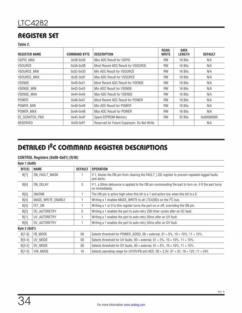
LTC4282
34Rev. A
For more information www.analog.com
REGISTER SETTable 2.
REGISTER NAME COMMAND BYTE DESCRIPTIONREAD/WRITE
DATA LENGTH DEFAULT
VGPIO_MAX 0x38-0x39 Max ADC Result for VGPIO RW 16 Bits N/A
VSOURCE 0x3A-0x3B Most Recent ADC Result for VSOURCE RW 16 Bits N/A
VSOURCE_MIN 0x3C-0x3D Min ADC Result for VSOURCE RW 16 Bits N/A
VSOURCE_MAX 0x3E-0x3F Max ADC Result for VSOURCE RW 16 Bits N/A
VSENSE 0x40-0x41 Most Recent ADC Result for VSENSE RW 16 Bits N/A
VSENSE_MIN 0x42-0x43 Min ADC Result for VSENSE RW 16 Bits N/A
VSENSE_MAX 0x44-0x45 Max ADC Result for VSENSE RW 16 Bits N/A
POWER 0x46-0x47 Most Recent ADC Result for POWER RW 16 Bits N/A
POWER_MIN 0x48-0x49 Min ADC Result for POWER RW 16 Bits N/A
POWER_MAX 0x4A-0x4B Max ADC Result for POWER RW 16 Bits N/A
EE_SCRATCH_PAD 0x4C-0x4F Spare EEPROM Memory RW 32 Bits 0x00000000
RESERVED 0x50-0xFF Reserved for Future Expansion, Do Not Write N/A
DETAILED I2C COMMAND REGISTER DESCRIPTIONSCONTROL Registers (0x00–0x01) (R/W)Byte 1 (0x00)
BIT(S) NAME DEFAULT OPERATION
B[7] ON_FAULT_MASK 1 If 1, blocks the ON pin from clearing the FAULT_LOG register to prevent repeated logged faults and alerts.
B[6] ON_DELAY 0 If 1, a 50ms debounce is applied to the ON pin commanding the part to turn on, if 0 the part turns on immediately.
B[5] ON/ENB 1 The ON pin is active high when this bit is a 1 and active low when this bit is a 0.
B[4] MASS_WRITE_ENABLE 1 Writing a 1 enables MASS_WRITE to all LTC4282s on the I2C bus.
B[3] FET_ON 1 Writing a 1 or 0 to this register turns the part on or off, overriding the ON pin.
B[2] OC_AUTORETRY 0 Writing a 1 enables the part to auto-retry 256 timer cycles after an OC fault.
B[1] UV_AUTORETRY 1 Writing a 1 enables the part to auto-retry 50ms after an UV fault.
B[0] OV_AUTORETRY 1 Writing a 1 enables the part to auto-retry 50ms after an OV fault.
Byte 2 (0x01)
B[7-6] FB_MODE 00 Selects threshold for POWER_GOOD, 00 = external, 01 = 5%, 10 = 10%, 11 = 15%.
B[5-4] UV_MODE 00 Selects threshold for UV faults, 00 = external, 01 = 5%, 10 = 10%, 11 = 15%.
B[3-2] OV_MODE 00 Selects threshold for OV faults, 00 = external, 01 = 5%, 10 = 10%, 11 = 15%.
B[1-0] VIN_MODE 10 Selects operating range for UV/OV/FB and ADC: 00 = 3.3V, 01 = 5V, 10 = 12V, 11 = 24V.
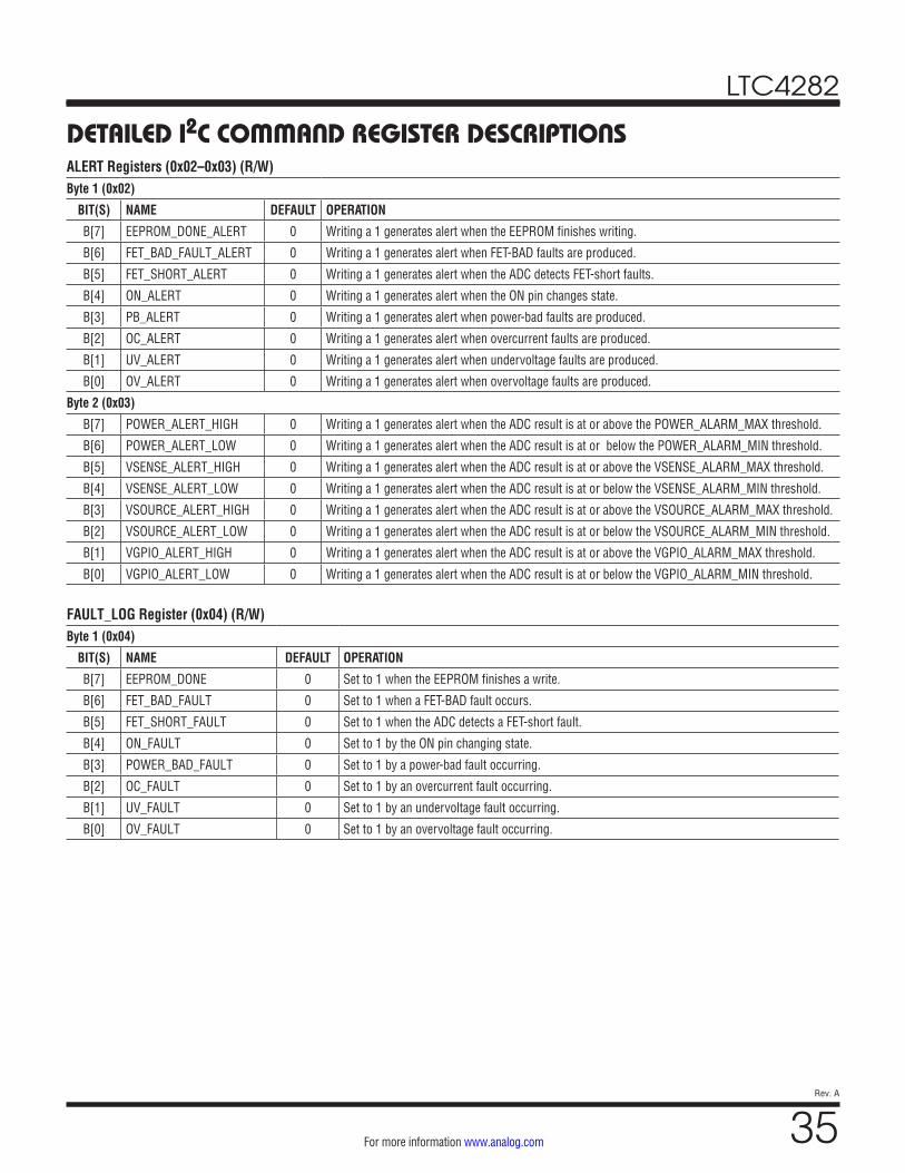
LTC4282
35Rev. A
For more information www.analog.com
DETAILED I2C COMMAND REGISTER DESCRIPTIONSALERT Registers (0x02–0x03) (R/W)Byte 1 (0x02)
BIT(S) NAME DEFAULT OPERATION
B[7] EEPROM_DONE_ALERT 0 Writing a 1 generates alert when the EEPROM finishes writing.
B[6] FET_BAD_FAULT_ALERT 0 Writing a 1 generates alert when FET-BAD faults are produced.
B[5] FET_SHORT_ALERT 0 Writing a 1 generates alert when the ADC detects FET-short faults.
B[4] ON_ALERT 0 Writing a 1 generates alert when the ON pin changes state.
B[3] PB_ALERT 0 Writing a 1 generates alert when power-bad faults are produced.
B[2] OC_ALERT 0 Writing a 1 generates alert when overcurrent faults are produced.
B[1] UV_ALERT 0 Writing a 1 generates alert when undervoltage faults are produced.
B[0] OV_ALERT 0 Writing a 1 generates alert when overvoltage faults are produced.
Byte 2 (0x03)
B[7] POWER_ALERT_HIGH 0 Writing a 1 generates alert when the ADC result is at or above the POWER_ALARM_MAX threshold.
B[6] POWER_ALERT_LOW 0 Writing a 1 generates alert when the ADC result is at or below the POWER_ALARM_MIN threshold.
B[5] VSENSE_ALERT_HIGH 0 Writing a 1 generates alert when the ADC result is at or above the VSENSE_ALARM_MAX threshold.
B[4] VSENSE_ALERT_LOW 0 Writing a 1 generates alert when the ADC result is at or below the VSENSE_ALARM_MIN threshold.
B[3] VSOURCE_ALERT_HIGH 0 Writing a 1 generates alert when the ADC result is at or above the VSOURCE_ALARM_MAX threshold.
B[2] VSOURCE_ALERT_LOW 0 Writing a 1 generates alert when the ADC result is at or below the VSOURCE_ALARM_MIN threshold.
B[1] VGPIO_ALERT_HIGH 0 Writing a 1 generates alert when the ADC result is at or above the VGPIO_ALARM_MAX threshold.
B[0] VGPIO_ALERT_LOW 0 Writing a 1 generates alert when the ADC result is at or below the VGPIO_ALARM_MIN threshold.
FAULT_LOG Register (0x04) (R/W)Byte 1 (0x04)
BIT(S) NAME DEFAULT OPERATION
B[7] EEPROM_DONE 0 Set to 1 when the EEPROM finishes a write.
B[6] FET_BAD_FAULT 0 Set to 1 when a FET-BAD fault occurs.
B[5] FET_SHORT_FAULT 0 Set to 1 when the ADC detects a FET-short fault.
B[4] ON_FAULT 0 Set to 1 by the ON pin changing state.
B[3] POWER_BAD_FAULT 0 Set to 1 by a power-bad fault occurring.
B[2] OC_FAULT 0 Set to 1 by an overcurrent fault occurring.
B[1] UV_FAULT 0 Set to 1 by an undervoltage fault occurring.
B[0] OV_FAULT 0 Set to 1 by an overvoltage fault occurring.
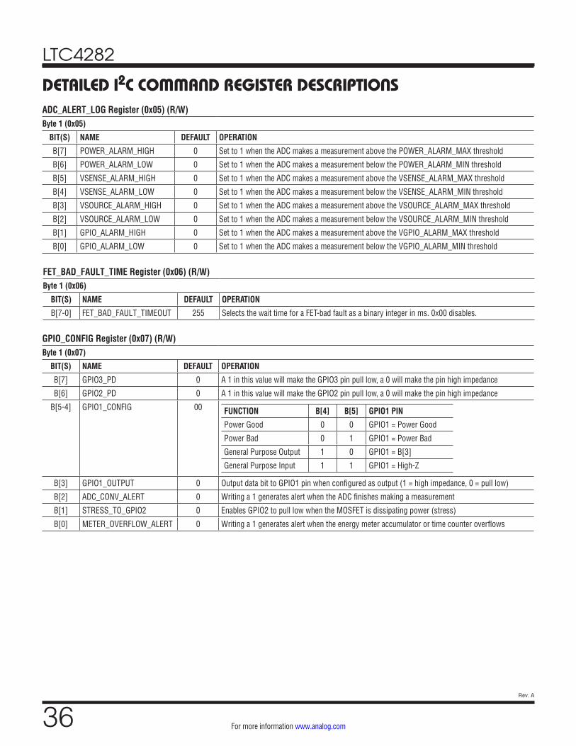
LTC4282
36Rev. A
For more information www.analog.com
FET_BAD_FAULT_TIME Register (0x06) (R/W)Byte 1 (0x06)
BIT(S) NAME DEFAULT OPERATION
B[7-0] FET_BAD_FAULT_TIMEOUT 255 Selects the wait time for a FET-bad fault as a binary integer in ms. 0x00 disables.
GPIO_CONFIG Register (0x07) (R/W)Byte 1 (0x07)
BIT(S) NAME DEFAULT OPERATION
B[7] GPIO3_PD 0 A 1 in this value will make the GPIO3 pin pull low, a 0 will make the pin high impedance
B[6] GPIO2_PD 0 A 1 in this value will make the GPIO2 pin pull low, a 0 will make the pin high impedance
B[5-4] GPIO1_CONFIG 00 FUNCTION B[4] B[5] GPIO1 PIN
Power Good 0 0 GPIO1 = Power Good
Power Bad 0 1 GPIO1 = Power Bad
General Purpose Output 1 0 GPIO1 = B[3]
General Purpose Input 1 1 GPIO1 = High-Z
B[3] GPIO1_OUTPUT 0 Output data bit to GPIO1 pin when configured as output (1 = high impedance, 0 = pull low)
B[2] ADC_CONV_ALERT 0 Writing a 1 generates alert when the ADC finishes making a measurement
B[1] STRESS_TO_GPIO2 0 Enables GPIO2 to pull low when the MOSFET is dissipating power (stress)
B[0] METER_OVERFLOW_ALERT 0 Writing a 1 generates alert when the energy meter accumulator or time counter overflows
DETAILED I2C COMMAND REGISTER DESCRIPTIONSADC_ALERT_LOG Register (0x05) (R/W)Byte 1 (0x05)
BIT(S) NAME DEFAULT OPERATION
B[7] POWER_ALARM_HIGH 0 Set to 1 when the ADC makes a measurement above the POWER_ALARM_MAX threshold
B[6] POWER_ALARM_LOW 0 Set to 1 when the ADC makes a measurement below the POWER_ALARM_MIN threshold
B[5] VSENSE_ALARM_HIGH 0 Set to 1 when the ADC makes a measurement above the VSENSE_ALARM_MAX threshold
B[4] VSENSE_ALARM_LOW 0 Set to 1 when the ADC makes a measurement below the VSENSE_ALARM_MIN threshold
B[3] VSOURCE_ALARM_HIGH 0 Set to 1 when the ADC makes a measurement above the VSOURCE_ALARM_MAX threshold
B[2] VSOURCE_ALARM_LOW 0 Set to 1 when the ADC makes a measurement below the VSOURCE_ALARM_MIN threshold
B[1] GPIO_ALARM_HIGH 0 Set to 1 when the ADC makes a measurement above the VGPIO_ALARM_MAX threshold
B[0] GPIO_ALARM_LOW 0 Set to 1 when the ADC makes a measurement below the VGPIO_ALARM_MIN threshold
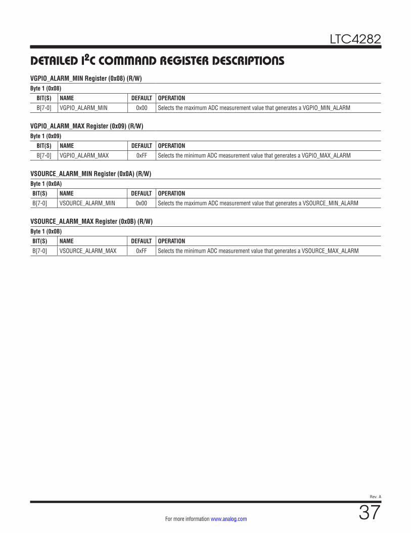
LTC4282
37Rev. A
For more information www.analog.com
DETAILED I2C COMMAND REGISTER DESCRIPTIONSVGPIO_ALARM_MIN Register (0x08) (R/W)Byte 1 (0x08)
BIT(S) NAME DEFAULT OPERATION
B[7-0] VGPIO_ALARM_MIN 0x00 Selects the maximum ADC measurement value that generates a VGPIO_MIN_ALARM
VGPIO_ALARM_MAX Register (0x09) (R/W)Byte 1 (0x09)
BIT(S) NAME DEFAULT OPERATION
B[7-0] VGPIO_ALARM_MAX 0xFF Selects the minimum ADC measurement value that generates a VGPIO_MAX_ALARM
VSOURCE_ALARM_MIN Register (0x0A) (R/W)Byte 1 (0x0A)
BIT(S) NAME DEFAULT OPERATION
B[7-0] VSOURCE_ALARM_MIN 0x00 Selects the maximum ADC measurement value that generates a VSOURCE_MIN_ALARM
VSOURCE_ALARM_MAX Register (0x0B) (R/W)Byte 1 (0x0B)
BIT(S) NAME DEFAULT OPERATION
B[7-0] VSOURCE_ALARM_MAX 0xFF Selects the minimum ADC measurement value that generates a VSOURCE_MAX_ALARM
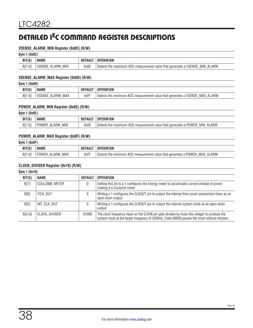
LTC4282
38Rev. A
For more information www.analog.com
DETAILED I2C COMMAND REGISTER DESCRIPTIONSVSENSE_ALARM_MIN Register (0x0C) (R/W)Byte 1 (0x0C)
BIT(S) NAME DEFAULT OPERATION
B[7-0] VSENSE_ALARM_MIN 0x00 Selects the maximum ADC measurement value that generates a VSENSE_MIN_ALARM
VSENSE_ALARM_MAX Register (0x0D) (R/W)Byte 1 (0x0D)
BIT(S) NAME DEFAULT OPERATION
B[7-0] VSENSE_ALARM_MAX 0xFF Selects the minimum ADC measurement value that generates a VSENSE_MAX_ALARM
POWER_ALARM_MAX Register (0x0F) (R/W)Byte 1 (0x0F)
BIT(S) NAME DEFAULT OPERATION
B[7-0] POWER_ALARM_MAX 0xFF Selects the minimum ADC measurement value that generates a POWER_MAX_ALARM
POWER_ALARM_MIN Register (0x0E) (R/W)Byte 1 (0x0E)
BIT(S) NAME DEFAULT OPERATION
B[7-0] POWER_ALARM_MIN 0x00 Selects the maximum ADC measurement value that generates a POWER_MIN_ALARM
CLOCK_DIVIDER Register (0x10) (R/W)Byte 1 (0x10)
BIT(S) NAME DEFAULT OPERATION
B[7] COULOMB_METER 0 Setting this bit to a 1 configures the Energy meter to accumulate current instead of power, making it a Coulomb meter
B[6] TICK_OUT 0 Writing a 1 configures the CLKOUT pin to output the internal time count (conversion time) as an open-drain output
B[5] INT_CLK_OUT 0 Writing a 1 configures the CLKOUT pin to output the internal system clock as an open-drain output
B[4-0] CLOCK_DIVIDER 01000 The clock frequency input on the CLKIN pin gets divided by twice this integer to produce the system clock at the target frequency of 250kHz. Code 00000 passes the clock without division
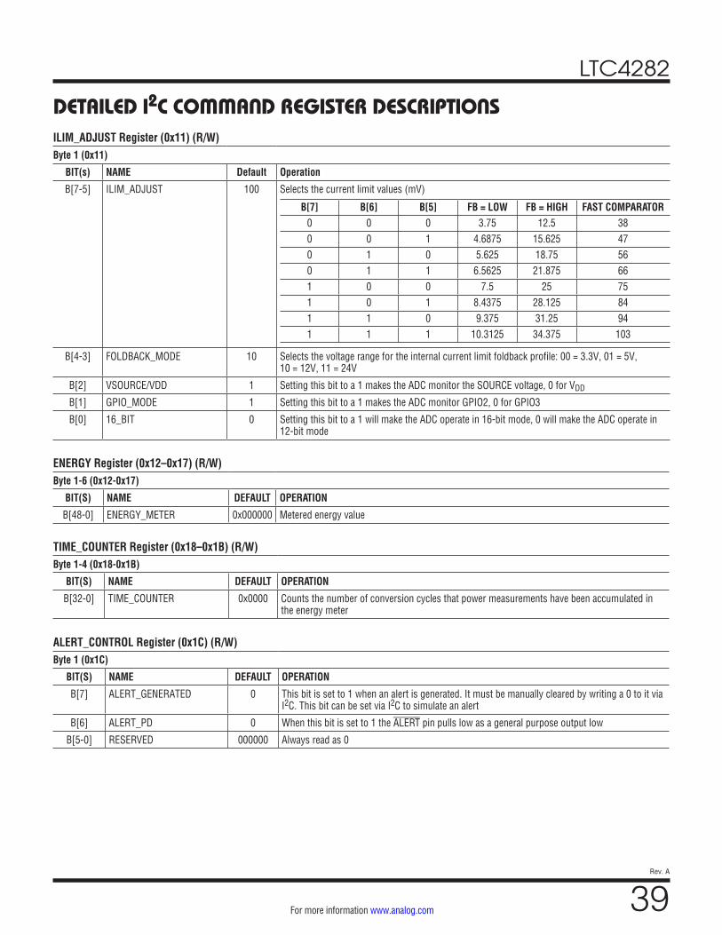
LTC4282
39Rev. A
For more information www.analog.com
DETAILED I2C COMMAND REGISTER DESCRIPTIONSILIM_ADJUST Register (0x11) (R/W)Byte 1 (0x11)
BIT(s) NAME Default Operation
B[7-5] ILIM_ADJUST 100 Selects the current limit values (mV)
B[7] B[6] B[5] FB = LOW FB = HIGH FAST COMPARATOR0 0 0 3.75 12.5 380 0 1 4.6875 15.625 470 1 0 5.625 18.75 560 1 1 6.5625 21.875 661 0 0 7.5 25 751 0 1 8.4375 28.125 841 1 0 9.375 31.25 941 1 1 10.3125 34.375 103
B[4-3] FOLDBACK_MODE 10 Selects the voltage range for the internal current limit foldback profile: 00 = 3.3V, 01 = 5V, 10 = 12V, 11 = 24V
B[2] VSOURCE/VDD 1 Setting this bit to a 1 makes the ADC monitor the SOURCE voltage, 0 for VDD
B[1] GPIO_MODE 1 Setting this bit to a 1 makes the ADC monitor GPIO2, 0 for GPIO3
B[0] 16_BIT 0 Setting this bit to a 1 will make the ADC operate in 16-bit mode, 0 will make the ADC operate in 12-bit mode
ENERGY Register (0x12–0x17) (R/W)Byte 1-6 (0x12-0x17)
BIT(S) NAME DEFAULT OPERATION
B[48-0] ENERGY_METER 0x000000 Metered energy value
TIME_COUNTER Register (0x18–0x1B) (R/W)Byte 1-4 (0x18-0x1B)
BIT(S) NAME DEFAULT OPERATION
B[32-0] TIME_COUNTER 0x0000 Counts the number of conversion cycles that power measurements have been accumulated in the energy meter
ALERT_CONTROL Register (0x1C) (R/W)Byte 1 (0x1C)
BIT(S) NAME DEFAULT OPERATION
B[7] ALERT_GENERATED 0 This bit is set to 1 when an alert is generated. It must be manually cleared by writing a 0 to it via I2C. This bit can be set via I2C to simulate an alert
B[6] ALERT_PD 0 When this bit is set to 1 the ALERT pin pulls low as a general purpose output low
B[5-0] RESERVED 000000 Always read as 0
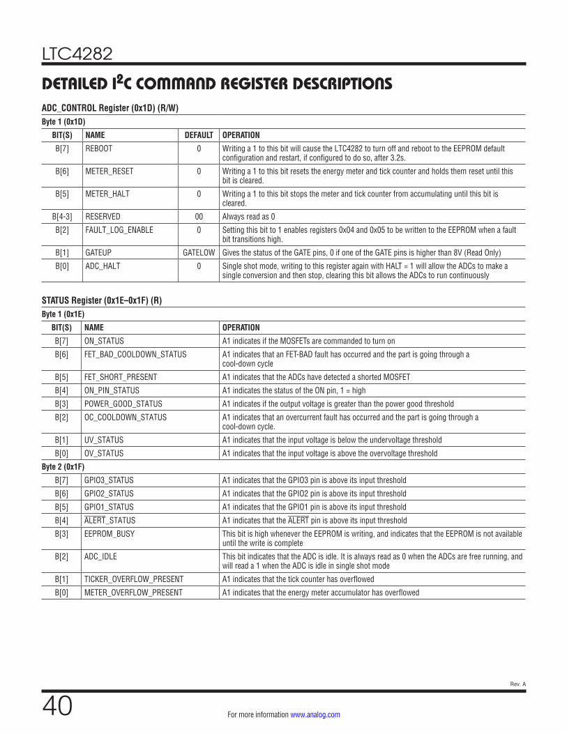
LTC4282
40Rev. A
For more information www.analog.com
DETAILED I2C COMMAND REGISTER DESCRIPTIONSADC_CONTROL Register (0x1D) (R/W)Byte 1 (0x1D)
BIT(S) NAME DEFAULT OPERATION
B[7] REBOOT 0 Writing a 1 to this bit will cause the LTC4282 to turn off and reboot to the EEPROM default configuration and restart, if configured to do so, after 3.2s.
B[6] METER_RESET 0 Writing a 1 to this bit resets the energy meter and tick counter and holds them reset until this bit is cleared.
B[5] METER_HALT 0 Writing a 1 to this bit stops the meter and tick counter from accumulating until this bit is cleared.
B[4-3] RESERVED 00 Always read as 0
B[2] FAULT_LOG_ENABLE 0 Setting this bit to 1 enables registers 0x04 and 0x05 to be written to the EEPROM when a fault bit transitions high.
B[1] GATEUP GATELOW Gives the status of the GATE pins, 0 if one of the GATE pins is higher than 8V (Read Only)
B[0] ADC_HALT 0 Single shot mode, writing to this register again with HALT = 1 will allow the ADCs to make a single conversion and then stop, clearing this bit allows the ADCs to run continuously
STATUS Register (0x1E–0x1F) (R)Byte 1 (0x1E)
BIT(S) NAME OPERATION
B[7] ON_STATUS A1 indicates if the MOSFETs are commanded to turn on
B[6] FET_BAD_COOLDOWN_STATUS A1 indicates that an FET-BAD fault has occurred and the part is going through a cool-down cycle
B[5] FET_SHORT_PRESENT A1 indicates that the ADCs have detected a shorted MOSFET
B[4] ON_PIN_STATUS A1 indicates the status of the ON pin, 1 = high
B[3] POWER_GOOD_STATUS A1 indicates if the output voltage is greater than the power good threshold
B[2] OC_COOLDOWN_STATUS A1 indicates that an overcurrent fault has occurred and the part is going through a cool-down cycle.
B[1] UV_STATUS A1 indicates that the input voltage is below the undervoltage threshold
B[0] OV_STATUS A1 indicates that the input voltage is above the overvoltage threshold
Byte 2 (0x1F)
B[7] GPIO3_STATUS A1 indicates that the GPIO3 pin is above its input threshold
B[6] GPIO2_STATUS A1 indicates that the GPIO2 pin is above its input threshold
B[5] GPIO1_STATUS A1 indicates that the GPIO1 pin is above its input threshold
B[4] ALERT_STATUS A1 indicates that the ALERT pin is above its input threshold
B[3] EEPROM_BUSY This bit is high whenever the EEPROM is writing, and indicates that the EEPROM is not available until the write is complete
B[2] ADC_IDLE This bit indicates that the ADC is idle. It is always read as 0 when the ADCs are free running, and will read a 1 when the ADC is idle in single shot mode
B[1] TICKER_OVERFLOW_PRESENT A1 indicates that the tick counter has overflowed
B[0] METER_OVERFLOW_PRESENT A1 indicates that the energy meter accumulator has overflowed
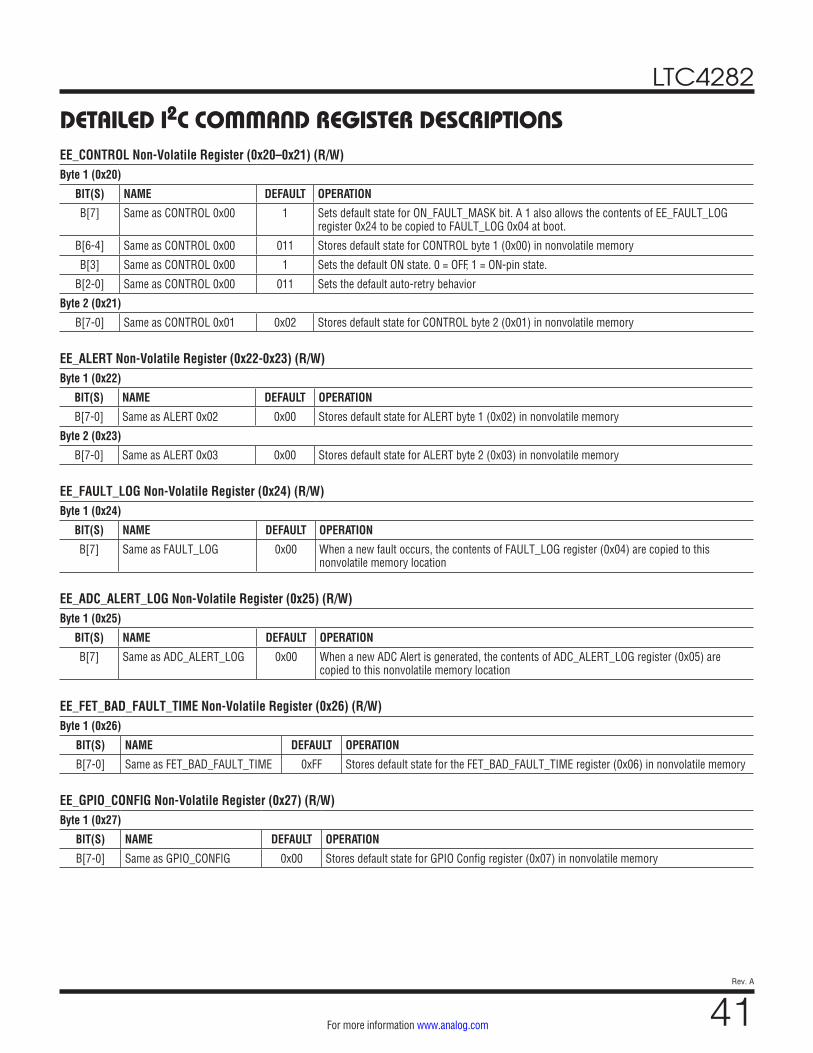
LTC4282
41Rev. A
For more information www.analog.com
DETAILED I2C COMMAND REGISTER DESCRIPTIONSEE_CONTROL Non-Volatile Register (0x20–0x21) (R/W)Byte 1 (0x20)
BIT(S) NAME DEFAULT OPERATION
B[7] Same as CONTROL 0x00 1 Sets default state for ON_FAULT_MASK bit. A 1 also allows the contents of EE_FAULT_LOG register 0x24 to be copied to FAULT_LOG 0x04 at boot.
B[6-4] Same as CONTROL 0x00 011 Stores default state for CONTROL byte 1 (0x00) in nonvolatile memory
B[3] Same as CONTROL 0x00 1 Sets the default ON state. 0 = OFF, 1 = ON-pin state.
B[2-0] Same as CONTROL 0x00 011 Sets the default auto-retry behavior
Byte 2 (0x21)
B[7-0] Same as CONTROL 0x01 0x02 Stores default state for CONTROL byte 2 (0x01) in nonvolatile memory
EE_ALERT Non-Volatile Register (0x22-0x23) (R/W)Byte 1 (0x22)
BIT(S) NAME DEFAULT OPERATION
B[7-0] Same as ALERT 0x02 0x00 Stores default state for ALERT byte 1 (0x02) in nonvolatile memory
Byte 2 (0x23)
B[7-0] Same as ALERT 0x03 0x00 Stores default state for ALERT byte 2 (0x03) in nonvolatile memory
EE_FAULT_LOG Non-Volatile Register (0x24) (R/W)Byte 1 (0x24)
BIT(S) NAME DEFAULT OPERATION
B[7] Same as FAULT_LOG 0x00 When a new fault occurs, the contents of FAULT_LOG register (0x04) are copied to this nonvolatile memory location
EE_ADC_ALERT_LOG Non-Volatile Register (0x25) (R/W)Byte 1 (0x25)
BIT(S) NAME DEFAULT OPERATION
B[7] Same as ADC_ALERT_LOG 0x00 When a new ADC Alert is generated, the contents of ADC_ALERT_LOG register (0x05) are copied to this nonvolatile memory location
EE_FET_BAD_FAULT_TIME Non-Volatile Register (0x26) (R/W)Byte 1 (0x26)
BIT(S) NAME DEFAULT OPERATION
B[7-0] Same as FET_BAD_FAULT_TIME 0xFF Stores default state for the FET_BAD_FAULT_TIME register (0x06) in nonvolatile memory
EE_GPIO_CONFIG Non-Volatile Register (0x27) (R/W)Byte 1 (0x27)
BIT(S) NAME DEFAULT OPERATION
B[7-0] Same as GPIO_CONFIG 0x00 Stores default state for GPIO Config register (0x07) in nonvolatile memory
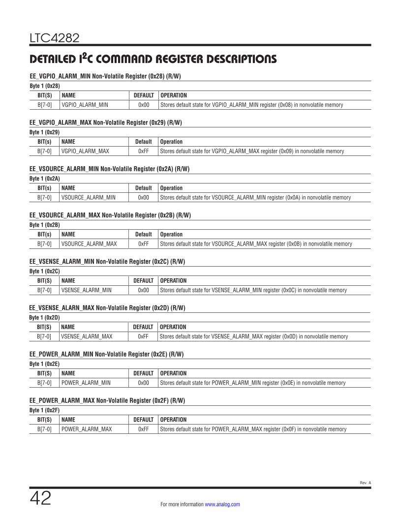
LTC4282
42Rev. A
For more information www.analog.com
DETAILED I2C COMMAND REGISTER DESCRIPTIONS
EE_VGPIO_ALARM_MAX Non-Volatile Register (0x29) (R/W)Byte 1 (0x29)
BIT(s) NAME Default Operation
B[7-0] VGPIO_ALARM_MAX 0xFF Stores default state for VGPIO_ALARM_MAX register (0x09) in nonvolatile memory
EE_VSOURCE_ALARM_MIN Non-Volatile Register (0x2A) (R/W)Byte 1 (0x2A)
BIT(s) NAME Default Operation
B[7-0] VSOURCE_ALARM_MIN 0x00 Stores default state for VSOURCE_ALARM_MIN register (0x0A) in nonvolatile memory
EE_VSOURCE_ALARM_MAX Non-Volatile Register (0x2B) (R/W)Byte 1 (0x2B)
BIT(s) NAME Default Operation
B[7-0] VSOURCE_ALARM_MAX 0xFF Stores default state for VSOURCE_ALARM_MAX register (0x0B) in nonvolatile memory
EE_VSENSE_ALARM_MIN Non-Volatile Register (0x2C) (R/W)Byte 1 (0x2C)
BIT(S) NAME DEFAULT OPERATION
B[7-0] VSENSE_ALARM_MIN 0x00 Stores default state for VSENSE_ALARM_MIN register (0x0C) in nonvolatile memory
EE_POWER_ALARM_MIN Non-Volatile Register (0x2E) (R/W)Byte 1 (0x2E)
BIT(S) NAME DEFAULT OPERATION
B[7-0] POWER_ALARM_MIN 0x00 Stores default state for POWER_ALARM_MIN register (0x0E) in nonvolatile memory
EE_POWER_ALARM_MAX Non-Volatile Register (0x2F) (R/W)Byte 1 (0x2F)
BIT(S) NAME DEFAULT OPERATION
B[7-0] POWER_ALARM_MAX 0xFF Stores default state for POWER_ALARM_MAX register (0x0F) in nonvolatile memory
EE_VSENSE_ALARN_MAX Non-Volatile Register (0x2D) (R/W)Byte 1 (0x2D)
BIT(S) NAME DEFAULT OPERATION
B[7-0] VSENSE_ALARM_MAX 0xFF Stores default state for VSENSE_ALARM_MAX register (0x0D) in nonvolatile memory
EE_VGPIO_ALARM_MIN Non-Volatile Register (0x28) (R/W)Byte 1 (0x28)
BIT(S) NAME DEFAULT OPERATION
B[7-0] VGPIO_ALARM_MIN 0x00 Stores default state for VGPIO_ALARM_MIN register (0x08) in nonvolatile memory
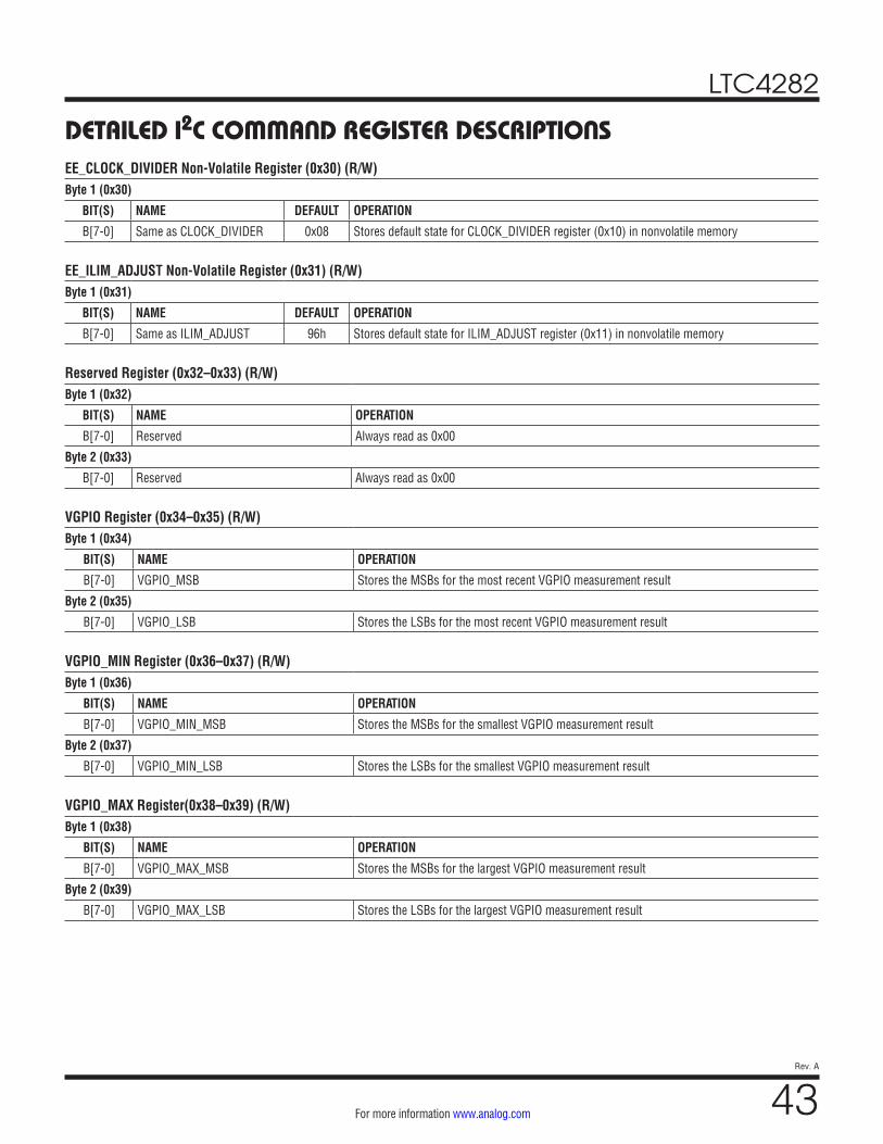
LTC4282
43Rev. A
For more information www.analog.com
DETAILED I2C COMMAND REGISTER DESCRIPTIONSEE_CLOCK_DIVIDER Non-Volatile Register (0x30) (R/W)Byte 1 (0x30)
BIT(S) NAME DEFAULT OPERATION
B[7-0] Same as CLOCK_DIVIDER 0x08 Stores default state for CLOCK_DIVIDER register (0x10) in nonvolatile memory
EE_ILIM_ADJUST Non-Volatile Register (0x31) (R/W)Byte 1 (0x31)
BIT(S) NAME DEFAULT OPERATION
B[7-0] Same as ILIM_ADJUST 96h Stores default state for ILIM_ADJUST register (0x11) in nonvolatile memory
Reserved Register (0x32–0x33) (R/W)Byte 1 (0x32)
BIT(S) NAME OPERATION
B[7-0] Reserved Always read as 0x00
Byte 2 (0x33)
B[7-0] Reserved Always read as 0x00
VGPIO Register (0x34–0x35) (R/W)Byte 1 (0x34)
BIT(S) NAME OPERATION
B[7-0] VGPIO_MSB Stores the MSBs for the most recent VGPIO measurement result
Byte 2 (0x35)
B[7-0] VGPIO_LSB Stores the LSBs for the most recent VGPIO measurement result
VGPIO_MIN Register (0x36–0x37) (R/W)Byte 1 (0x36)
BIT(S) NAME OPERATION
B[7-0] VGPIO_MIN_MSB Stores the MSBs for the smallest VGPIO measurement result
Byte 2 (0x37)
B[7-0] VGPIO_MIN_LSB Stores the LSBs for the smallest VGPIO measurement result
VGPIO_MAX Register(0x38–0x39) (R/W)Byte 1 (0x38)
BIT(S) NAME OPERATION
B[7-0] VGPIO_MAX_MSB Stores the MSBs for the largest VGPIO measurement result
Byte 2 (0x39)
B[7-0] VGPIO_MAX_LSB Stores the LSBs for the largest VGPIO measurement result
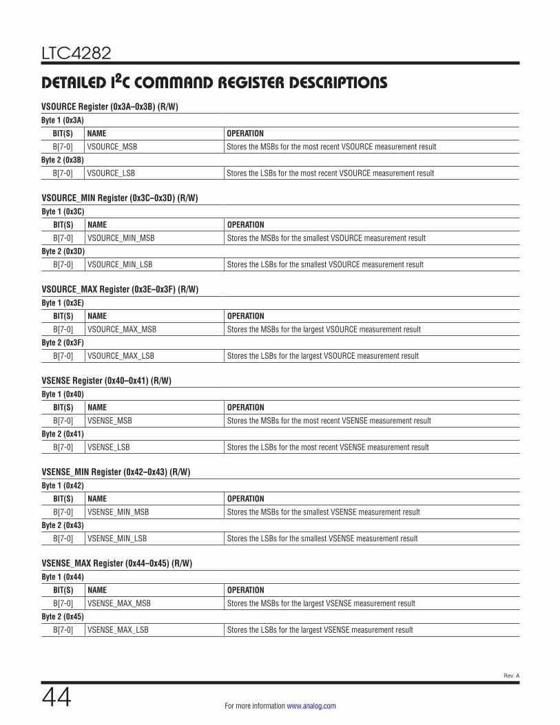
LTC4282
44Rev. A
For more information www.analog.com
VSOURCE_MIN Register (0x3C–0x3D) (R/W)Byte 1 (0x3C)
BIT(S) NAME OPERATION
B[7-0] VSOURCE_MIN_MSB Stores the MSBs for the smallest VSOURCE measurement result
Byte 2 (0x3D)
B[7-0] VSOURCE_MIN_LSB Stores the LSBs for the smallest VSOURCE measurement result
VSOURCE_MAX Register (0x3E–0x3F) (R/W)Byte 1 (0x3E)
BIT(S) NAME OPERATION
B[7-0] VSOURCE_MAX_MSB Stores the MSBs for the largest VSOURCE measurement result
Byte 2 (0x3F)
B[7-0] VSOURCE_MAX_LSB Stores the LSBs for the largest VSOURCE measurement result
VSENSE Register (0x40–0x41) (R/W)Byte 1 (0x40)
BIT(S) NAME OPERATION
B[7-0] VSENSE_MSB Stores the MSBs for the most recent VSENSE measurement result
Byte 2 (0x41)
B[7-0] VSENSE_LSB Stores the LSBs for the most recent VSENSE measurement result
VSENSE_MIN Register (0x42–0x43) (R/W)Byte 1 (0x42)
BIT(S) NAME OPERATION
B[7-0] VSENSE_MIN_MSB Stores the MSBs for the smallest VSENSE measurement result
Byte 2 (0x43)
B[7-0] VSENSE_MIN_LSB Stores the LSBs for the smallest VSENSE measurement result
VSENSE_MAX Register (0x44–0x45) (R/W)Byte 1 (0x44)
BIT(S) NAME OPERATION
B[7-0] VSENSE_MAX_MSB Stores the MSBs for the largest VSENSE measurement result
Byte 2 (0x45)
B[7-0] VSENSE_MAX_LSB Stores the LSBs for the largest VSENSE measurement result
DETAILED I2C COMMAND REGISTER DESCRIPTIONSVSOURCE Register (0x3A–0x3B) (R/W)Byte 1 (0x3A)
BIT(S) NAME OPERATION
B[7-0] VSOURCE_MSB Stores the MSBs for the most recent VSOURCE measurement result
Byte 2 (0x3B)
B[7-0] VSOURCE_LSB Stores the LSBs for the most recent VSOURCE measurement result
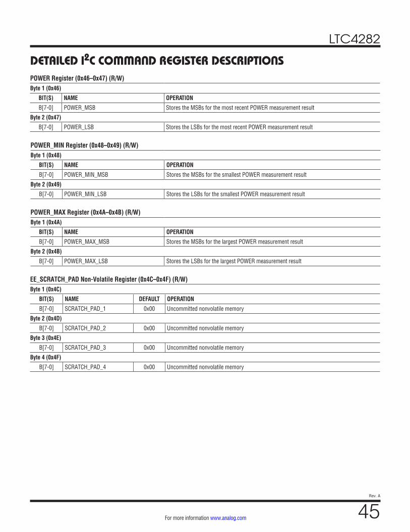
LTC4282
45Rev. A
For more information www.analog.com
POWER Register (0x46–0x47) (R/W)Byte 1 (0x46)
BIT(S) NAME OPERATION
B[7-0] POWER_MSB Stores the MSBs for the most recent POWER measurement result
Byte 2 (0x47)
B[7-0] POWER_LSB Stores the LSBs for the most recent POWER measurement result
POWER_MIN Register (0x48–0x49) (R/W)Byte 1 (0x48)
BIT(S) NAME OPERATION
B[7-0] POWER_MIN_MSB Stores the MSBs for the smallest POWER measurement result
Byte 2 (0x49)
B[7-0] POWER_MIN_LSB Stores the LSBs for the smallest POWER measurement result
POWER_MAX Register (0x4A–0x4B) (R/W)Byte 1 (0x4A)
BIT(S) NAME OPERATION
B[7-0] POWER_MAX_MSB Stores the MSBs for the largest POWER measurement result
Byte 2 (0x4B)
B[7-0] POWER_MAX_LSB Stores the LSBs for the largest POWER measurement result
EE_SCRATCH_PAD Non-Volatile Register (0x4C–0x4F) (R/W)Byte 1 (0x4C)
BIT(S) NAME DEFAULT OPERATION
B[7-0] SCRATCH_PAD_1 0x00 Uncommitted nonvolatile memory
Byte 2 (0x4D)
B[7-0] SCRATCH_PAD_2 0x00 Uncommitted nonvolatile memory
Byte 3 (0x4E)
B[7-0] SCRATCH_PAD_3 0x00 Uncommitted nonvolatile memory
Byte 4 (0x4F)
B[7-0] SCRATCH_PAD_4 0x00 Uncommitted nonvolatile memory
DETAILED I2C COMMAND REGISTER DESCRIPTIONS
LTC4282
46Rev. A
For more information www.analog.com
12V, 100A Backplane Resident Parallel Application
TYPICAL APPLICATIONS
+
VDD GATE1 GATE2
CTIMER10nF
TIMER
LTC4282
4MHz
ABLS-4.000MHZ-B4-T
INTVCC
CONN
ECTO
R 1
CONN
ECTO
R 2
PLUG-INBOARD
NC
R134.0k1%
R510Ω
R410Ω
RS10.5mΩ
RS20.5mΩ
SOURCE
FBGPIO1GPIO2GPIO3
SDAISDAO
SCLALERT
ON
UV
OV
ADR0ADR1ADR2
SENSE2+ SENSE1+ SENSE1– SENSE2–ADC+
R151Ω
R141Ω
R121Ω
R131Ω
ADC–
WP GND
12V
CLKOUTCLKIN
C31µF C4
33pFC533pF
BACKPLANE
R21.18k1%
CF0.1µF25V
12V
GND
CS470µF
R33.4k1%
R728.7k1%
R83.57k1%
GPGP
R910k1%
R1010k5%
+ SDASCLALERT
POWER GOOD
4282 TA03
CL
VOUT12V100A ADJUSTABLE
Q2 ×2PSMN1R5-30BLE
Q1 ×2PSMN1R5-30BLE
LTC4282
47Rev. A
For more information www.analog.com
TYPICAL APPLICATIONS200A Low Stress Staged Start Application, See DC2442 for More Information
25A SEGMENT×7
4282 TA04
+
VDDSMCJ-28A×5
GATE1 GATE2
CTIMER22nF1.4ms
TIMER
LTC4282
INTVCC
CONN
ECTO
R 1
CONN
ECTO
R 2
PLUG-INBOARD
NC
GND
SDASCL
ALERT
R510Ω
R20100Ω
CL
R7659k
C120.82µF
R722.1k1%R83.01k1%
VOUT12V52.5A
R695mΩ
SOURCE
FB
GPIO1GPIO2GPIO3
GPGP
UVOVSDAISDAOSCLALERTADR0ADR1ADR2ON
SENSE2+ SENSE1+ SENSE1– SENSE2–ADC+
R680.5Ω
R670.5Ω
Q1 TRICKLEPSMN011-30YLC
R561mΩ
R541Ω
R551Ω
R570.1Ω
R580.1Ω R70
10Ω
Q2PSMNOR9
-30YLD
ADC–
WP GNDCLKOUTCLKIN
Y14MHz
ABLS-4.000MHZ-B4-T
C34.7µF
C436pF
C536pF
12V
BACKPLANE
R21.18k1%
R334.0k1%
R13.4k1%
CF0.1µF25V
PG
R924k
R7559k
C110.022µF
R611mΩ
R591Ω
R601Ω
R620.1Ω
R630.1Ω
R461mΩ
R441Ω
R451Ω
R470.1Ω
R480.1Ω R71
10Ω
Q3PSMNOR9
-30YLD
R511mΩ
R491Ω
R501Ω
R520.1Ω
R530.1Ω
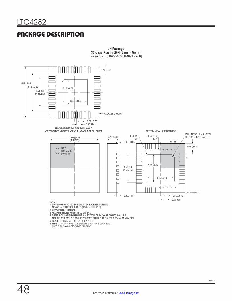
LTC4282
48Rev. A
For more information www.analog.com
PACKAGE DESCRIPTION
5.00 ±0.10(4 SIDES)
NOTE:1. DRAWING PROPOSED TO BE A JEDEC PACKAGE OUTLINE M0-220 VARIATION WHHD-(X) (TO BE APPROVED)2. DRAWING NOT TO SCALE3. ALL DIMENSIONS ARE IN MILLIMETERS4. DIMENSIONS OF EXPOSED PAD ON BOTTOM OF PACKAGE DO NOT INCLUDE MOLD FLASH. MOLD FLASH, IF PRESENT, SHALL NOT EXCEED 0.20mm ON ANY SIDE5. EXPOSED PAD SHALL BE SOLDER PLATED6. SHADED AREA IS ONLY A REFERENCE FOR PIN 1 LOCATION ON THE TOP AND BOTTOM OF PACKAGE
PIN 1TOP MARK(NOTE 6)
0.40 ±0.10
31
1
2
32
BOTTOM VIEW—EXPOSED PAD
3.50 REF(4-SIDES)
3.45 ±0.10
3.45 ±0.10
0.75 ±0.05 R = 0.115TYP
0.25 ±0.05(UH32) QFN 0406 REV D
0.50 BSC
0.200 REF
0.00 – 0.05
0.70 ±0.05
3.50 REF(4 SIDES)
4.10 ±0.05
5.50 ±0.05
0.25 ±0.05
PACKAGE OUTLINE
0.50 BSC
RECOMMENDED SOLDER PAD LAYOUTAPPLY SOLDER MASK TO AREAS THAT ARE NOT SOLDERED
PIN 1 NOTCH R = 0.30 TYPOR 0.35 × 45° CHAMFERR = 0.05
TYP
3.45 ±0.05
3.45 ±0.05
UH Package32-Lead Plastic QFN (5mm × 5mm)
(Reference LTC DWG # 05-08-1693 Rev D)
LTC4282
49Rev. A
For more information www.analog.com
Information furnished by Analog Devices is believed to be accurate and reliable. However, no responsibility is assumed by Analog Devices for its use, nor for any infringements of patents or other rights of third parties that may result from its use. Specifications subject to change without notice. No license is granted by implication or otherwise under any patent or patent rights of Analog Devices.
REVISION HISTORYREV DATE DESCRIPTION PAGE NUMBER
A 12/18 Updated graph for MOSFET Power Limit (G05) Added a section on constant current startup Added DG to Figure 4 Updated equations to calculate R2, R3, and R7 Updated sections: Resetting Faults in FAULT_LOG, Layout Considerations, EEPROM, EE_CONTROL register, Typical Application
7 15 18
27, 28 23, 28, 31,
41, 46
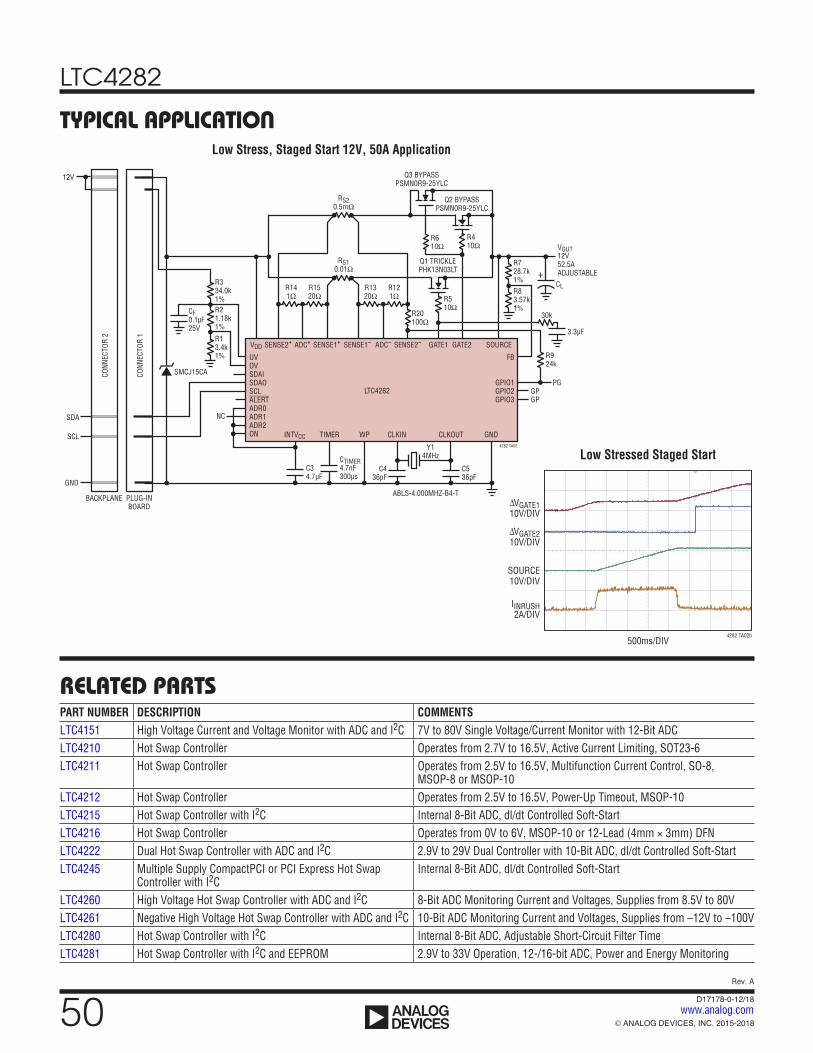
LTC4282
50Rev. A
For more information www.analog.com ANALOG DEVICES, INC. 2015-2018
D17178-0-12/18www.analog.com
RELATED PARTS
TYPICAL APPLICATIONLow Stress, Staged Start 12V, 50A Application
PART NUMBER DESCRIPTION COMMENTSLTC4151 High Voltage Current and Voltage Monitor with ADC and I2C 7V to 80V Single Voltage/Current Monitor with 12-Bit ADCLTC4210 Hot Swap Controller Operates from 2.7V to 16.5V, Active Current Limiting, SOT23-6LTC4211 Hot Swap Controller Operates from 2.5V to 16.5V, Multifunction Current Control, SO-8,
MSOP-8 or MSOP-10LTC4212 Hot Swap Controller Operates from 2.5V to 16.5V, Power-Up Timeout, MSOP-10LTC4215 Hot Swap Controller with I2C Internal 8-Bit ADC, dl/dt Controlled Soft-StartLTC4216 Hot Swap Controller Operates from 0V to 6V, MSOP-10 or 12-Lead (4mm × 3mm) DFNLTC4222 Dual Hot Swap Controller with ADC and I2C 2.9V to 29V Dual Controller with 10-Bit ADC, dl/dt Controlled Soft-StartLTC4245 Multiple Supply CompactPCI or PCI Express Hot Swap
Controller with I2CInternal 8-Bit ADC, dl/dt Controlled Soft-Start
LTC4260 High Voltage Hot Swap Controller with ADC and I2C 8-Bit ADC Monitoring Current and Voltages, Supplies from 8.5V to 80VLTC4261 Negative High Voltage Hot Swap Controller with ADC and I2C 10-Bit ADC Monitoring Current and Voltages, Supplies from –12V to –100VLTC4280 Hot Swap Controller with I2C Internal 8-Bit ADC, Adjustable Short-Circuit Filter TimeLTC4281 Hot Swap Controller with I2C and EEPROM 2.9V to 33V Operation, 12-/16-bit ADC, Power and Energy Monitoring
Low Stressed Staged Start
500ms/DIV
SOURCE10V/DIV
IINRUSH2A/DIV
∆VGATE110V/DIV
∆VGATE210V/DIV
4282 TA02b
+
VDD
SMCJ15CA
GATE1 GATE2
CTIMER4.7nF300µs
TIMER
LTC4282
INTVCC
CONN
ECTO
R 1
CONN
ECTO
R 2
PLUG-INBOARD
NC
4282 TA02
GND
R510Ω
R20100Ω
CL
30k
3.3µF
R410Ω
R610Ω
R728.7k1%R83.57k1%
VOUT12V52.5AADJUSTABLE
RS20.5mΩ
RS10.01Ω
SOURCE
FB
GPIO1GPIO2GPIO3
GPGP
UVOVSDAISDAOSCLALERTADR0ADR1ADR2ON
SENSE2+ SENSE1+ SENSE1– SENSE2–ADC+
R141Ω
R1520Ω
R1320Ω
R121Ω
Q1 TRICKLEPHK13N03LT
Q2 BYPASSPSMN0R9-25YLC
Q3 BYPASSPSMN0R9-25YLC
ADC–
WP GNDCLKOUTCLKIN
Y14MHz
ABLS-4.000MHZ-B4-T
C34.7µF
C436pF
C536pF
12V
BACKPLANE
SCL
SDA
R21.18k1%
R334.0k1%
R13.4k1%
CF0.1µF25V
PG
R924k