Embed Size (px)
Citation preview

LTC3106
13106f
For more information www.linear.com/LTC3106
Typical applicaTion
FeaTures DescripTion
300mA Low Voltage Buck-Boost Converter with
PowerPath and 1.6µA Quiescent Current
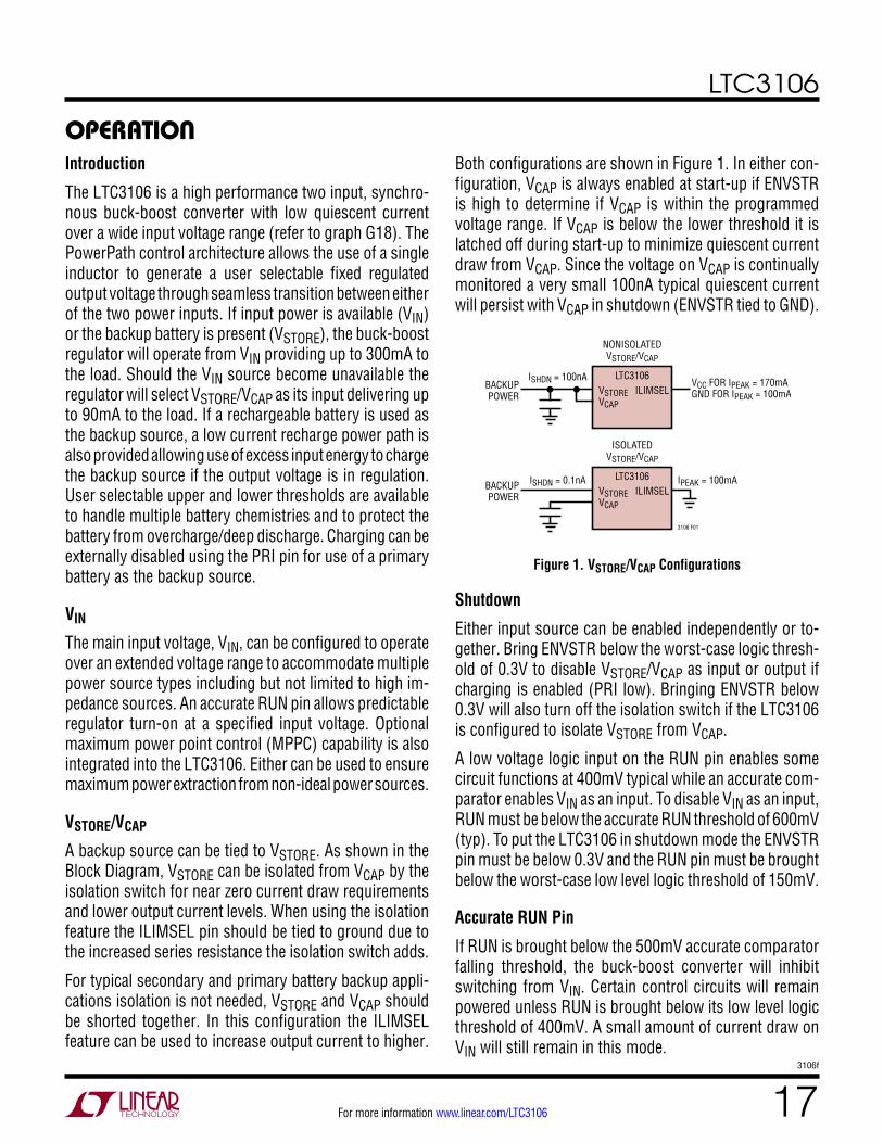
The LTC®3106 is a highly integrated, ultralow voltage buck-boost DC/DC converter with automatic PowerPath man-agement optimized for multisource, low power systems.At no load, the LTC3106 draws only 1.6µA while creating an output voltage up to 5V from either input source.
If the primary power source is unavailable, the LTC3106 seamlessly switches to the backup power source. The LTC3106 is compatible with either rechargeable or pri-mary cell batteries and can trickle charge a backup battery whenever there is an energy surplus available. Optional maximum power point control ensures power transfer is optimized between power source and load. The output volt-age and backup voltage, VSTORE, are programmed digitally, reducing the required number of external components. Zero power Shelf Mode ensures that the backup battery will remain charged if left connected to the LTC3106 for an extended time.
Additional features include an accurate turn-on voltage, a power good indicator for VOUT, a user selectable 100mA peak current limit setting for lower power applications, thermal shutdown as well as user selectable backup power and output voltages.
applicaTions
n Dual Input Buck-Boost with Integrated PowerPath™ Managern Ultralow Start-Up Voltages: 850mV Start with No
Backup Source, 300mV with a Backup Sourcen Compatible with Primary or Rechargeable Backup
Batteriesn Digitally Selectable VOUT and VSTOREn Maximum Power Point Controln Ultralow Quiescent Current: 1.6μAn Regulated Output with VIN or VSTORE Above, Below or Equal to the Outputn Optional Backup Battery Trickle Chargern Shelf Mode Disconnect Function to Preserve Battery
Shelf Lifen Burst Mode® Operationn Accurate RUN Pin Thresholdn Power Good Output Voltage Indicatorn Selectable Peak Current Limit: 90mA/650mAn Available in Thermally Enhanced 3mm × 4mm 16-Pin
QFN and 20-Pin TSSOP Packages
n Wireless Sensor Networksn Home or Office Building Automationn Energy Harvestingn Remote Sensors
L, LT, LTC, LTM, Linear Technology, the Linear logo, Eterna and Burst Mode are registered trademarks and PowerPath is a trademark of Linear Technology Corporation. All other trademarks are the property of their respective owners. Protected by U.S. Patents, including 7432695 and 6366066.
Efficiency vs Input VoltageSolar Cell Input with Primary Battery Backup
+
+
10µH
VSTOREVCAPENVSTRRUN
VCCPRI
VAUXTL-5955
PRIMARYBATTERY
3.6V
600mV TO 5VPV CELLS
VOUT
PGOOD
MPPILIMSEL
GND
LTC3106
VIN
1M
VCC
PGOOD
3106 TA01a
2.2µF
47µF
3.3V50mA
10µF
1µF
0.01µF
470µF
SW1 SW2
VIN EFF.VIN P.L.VSTR EFF.VSTR P.L.
INPUT VOLTAGE (V)0.5 1 1.5 2 2.5 3 3.5 4 4.5 5 5.5
40
45
50
55
60
65
70
75
80
85
90
95
100
0
10
20
30
40
50
60
70
80
90
100
110
EFFI
CIEN
CY (%
)
POWER LOSS (m
W)
LTC3106 TA01b
IOUT = 50mA
LTC3106
23106f
For more information www.linear.com/LTC3106
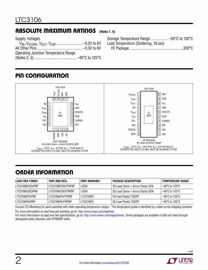
pin conFiguraTion
absoluTe MaxiMuM raTingsSupply Voltages VIN, VSTORE, VOUT, VCAP ........................... –0.3V to 6VAll Other Pins ............................................... –0.3V to 6VOperating Junction Temperature Range(Notes 2, 3) ............................................ –40°C to 125°C
(Notes 1, 6)
20 19 18 17
7 8
TOP VIEW
21GND
UDC PACKAGE20-LEAD (3mm × 4mm) PLASTIC QFN
9 10
6
5
4
3
2
1
11
12
13
14
15
16NC
VOUT
VAUX
VCC
OS1
OS2
VIN
GND
ENVSTR
RUN
ILIMSEL
PRI
V CAP
V STO
RE
SW1
SW2
PGOO
D
MPP SS
2
SS1
TJMAX = 125°C, θJA = 52°C/W, θJC = 7°C/W (Note 5)
EXPOSED PAD (PIN 21) IS GND, MUST BE SOLDERED TO PCB
FE PACKAGE20-LEAD PLASTIC TSSOP
1
2
3
4
5
6
7
8
9
10
TOP VIEW
20
19
18
17
16
15
14
13
12
11
VSTORE
VCAP
VOUT
NC
VAUX
VCC
OS1
OS2
PGOOD
MPP
SW1
SW2
VIN
GND
ENVSTR
RUN
ILIMSEL
PRI
SS1
SS2
21GND
TJMAX = 125°C, θJA = 48.6°C/W, θJC = 8.6°C/W (Note 5)
EXPOSED PAD (PIN 21) IS GND, MUST BE SOLDERED TO PCB
orDer inForMaTionLEAD FREE FINISH TAPE AND REEL PART MARKING* PACKAGE DESCRIPTION TEMPERATURE RANGE
LTC3106EUDC#PBF LTC3106EUDC#TRPBF LGQH 20-Lead (3mm × 4mm) Plastic QFN –40°C to 125°C
LTC3106IUDC#PBF LTC3106IUDC#TRPBF LGQH 20-Lead (3mm × 4mm) Plastic QFN –40°C to 125°C
LTC3106EFE#PBF LTC3106EFE#TRPBF LTC3106FE 20-Lead Plastic TSSOP –40°C to 125°C
LTC3106IFE#PBF LTC3106IFE#TRPBF LTC3106FE 20-Lead Plastic TSSOP –40°C to 125°C
Consult LTC Marketing for parts specified with wider operating temperature ranges. *The temperature grade is identified by a label on the shipping containerFor more information on lead free part marking, go to: http://www.linear.com/leadfree/ For more information on tape and reel specifications, go to: http://www.linear.com/tapeandreel/. Some packages are available in 500 unit reels through designated sales channels with #TRMPBF suffix.
Storage Temperature Range .................. –65°C to 150°CLead Temperature (Soldering, 10 sec) FE Package ....................................................... 300°C
LTC3106
33106f
For more information www.linear.com/LTC3106
elecTrical characTerisTics The l denotes the specifications which apply over the specified junction temperature range, otherwise specifications are at TA = 25°C (Note 2). VIN = 1.5V, VOUT = 3.3V, VSTORE = 3.6V and VAUX in regulation unless otherwise noted.PARAMETER CONDITIONS MIN TYP MAX UNITSVIN Start-Up Voltage Start-Up from VIN, VOUT = VAUX = VSTORE = 0V, RUN = VIN l 0.85 1.2 VVIN Maximum Operating Voltage 5.1 VVIN Minimum Operating Voltage VSTORE in Operating Voltage Limits, RUN > 0.613V,
ENVSTR Pin > 0.8V (Minimum Voltage Is Load Dependent)l 0.25 0.3 0.35 V
VIN Minimum No-Load Start-Up Power Start-Up from VIN, RUN = VIN, VOUT = VAUX = VSTORE = 0V 12 µW VIN Undervoltage Quiescent Current Start-Up from VIN, RUN = VIN, VOUT = VAUX = VSTORE = 0V l 1 2 µAShutdown Current – VIN VSTORE = 0V, RUN = 0
TJ = –40°C to 85°C (Note 4)l 300
300750 450
nA nA
Quiescent Current – VIN Switching Enabled, VOUT in Regulation, Non-Switching l 0.1 1 µASwitching Enabled, VOUT in Regulation, Non-Switching, TJ = –40°C to 85°C (Note 4)
0.1 0.3 µA
VSTORE Maximum Operating Voltage PRI = VCC, ENVSTR = VSTORE l 4.3 VVSTORE Minimum Operating Voltage VOUT in Regulation, VCAP Shorted to VSTORE, PRI = VCC,
ENVSTR = VSTORE
2.1 V
VSTORE Under Voltage Lockout PRI = VCC, ENVSTR = VSTORE l 1.730 1.778 1.826 VVSTORE Operating Voltage (Note 7) SS1 = 0V, SS2 = 0V OV
UVl
l
3.90 2.70
4.00 2.78
4.10 2.86
V V
SS1 = 0V, SS2 = VCC OV UV
l
l
2.81 1.85
2.90 1.90
2.99 1.95
V V
SS1 = VCC, SS2 = 0V OV UV
l
l
2.91 2.08
3.00 2.15
3.08 2.21
V V
SS1 = VCC, SS2 = VCC OV UV
l
l
3.90 2.91
4.00 3.00
4.10 3.08
V V
Output Regulation Voltage 1.8V VOUT Selected TJ = –40°C to 85°C (Note 4)
l 1.75 1.8 1.85 V1.755 1.8 1.845 V
2.2V VOUT Selected TJ = –40°C to 85°C (Note 4)
l 2.14 2.2 2.25 V2.145 2.2 2.245 V
3.3V VOUT Selected TJ = –40°C to 85°C (Note 4)
l 3.22 3.3 3.40 V3.23 3.3 3.38 V
5V VOUT Selected TJ = –40°C to 85°C (Note 4)
l 4.90 5.0 5.10 V4.92 5.0 5.08 V
Quiescent Current – VAUX Enabled, VOUT in Regulation, Non-Switching, TJ = –40°C to 85°C (Note 4)
l 1.6 1.6
3 2.5
µA µA
Quiescent Current – VOUT Enabled, VOUT in Regulation, Non-Switching, TJ = –40°C to 85°C (Note 4)
l 0.1 0.1
1 0.3
µA µA
Quiescent Current – VSTORE Enabled, VOUT in Regulation, Non-Switching, VCAP Shorted to VSTORE TJ = –40°C to 85°C (Note 4)
l 0.1
0.1
1
0.3
µA
µAShutdown Current – VSTORE VIN = 0V, VCAP Shorted to VSTORE, ENVSTR = 0V
TJ = –40°C to 85°C (Note 4) l 0.1
0.10.7 0.3
µA µA
Shelf Mode VSTORE Leakage Current Isolated VSTORE, ENVSTR = 0V 0.1 25 nA N-Channel MOSFETs – Leakage Current B and C Switches 0.1 1 µAP-Channel MOSFETs – Leakage Current A1, A2, D1 and D2 Switches 0.1 1 µAN-Channel MOSFET B and C Switch RDS(ON) VIN = 5V 0.5 ΩP-Channel MOSFET A1 RDS(ON) VIN = 5V 0.5 ΩP-Channel MOSFET A2 RDS(ON) VSTORE = VCAP = 4.2V 1.9 ΩP-Channel MOSFET D1 RDS(ON) VOUT = 3.3V 0.9 ΩP-Channel MOSFET D2 RDS(ON) VSTORE = VCAP = 4.2V 2.9 Ω
LTC3106
43106f
For more information www.linear.com/LTC3106
PARAMETER CONDITIONS MIN TYP MAX UNITSP-Channel MOSFET AUXSW RDS(ON) VAUX = 5.4V 3 ΩP-Channel VSTORE Isolation MOSFET RDS(ON) VSTORE = 4.2V 2 ΩPeak Current Limit (VOUT) VOUT Powered from VIN, ILIMSEL > 0.8V
VOUT Powered from VIN, ILIMSEL = 0V VOUT Powered from VSTORE, ILIMSEL > 0.8V VOUT Powered from VSTORE, ILIMSEL = 0V
l
l
l
l
530 60
140 60
725 100 200 100
mA mA mA mA
VALLEY Current Limit VOUT Powered from VIN, ILIMSEL > 0.8V VOUT Powered from VIN, ILIMSEL = 0V VOUT Powered from VSTORE, ILIMSEL > 0.8V VOUT Powered from VSTORE, ILIMSEL = 0V
l
l
l
l
300 10 30 10
400 44 70 44
mA mA mA mA
Peak Current Limit (VSTORE Charging) VSTORE Powered from VIN l 60 100 mAPGOOD Threshold VOUT Falling, Percentage Below VOUT –11 –9 –7 %PGOOD Hysteresis Percentage of VOUT 3 %PGOOD Voltage Low IPGOOD = 100µA 0.2 VPGOOD Leakage Current VPGOOD = 5V 0.1 10 nAVIH Digital Input High Logic Level Pins: OS[1:2], SS[1:2], ILIMSEL, ENVSTR, PRI l 0.8 VVIL Digital Input Low Logic Level Pins: OS[1:2], SS[1:2], ILIMSEL, ENVSTR, PRI l 0.3 VDigital Input Leakage Current Pin Voltage = 5.2V,
Pins: OS[1:2], SS[1:2], ILIMSEL, PRI0.1 10 nA
ENVSTR Input Leakage Current l 44 80 nAAuxiliary Voltage Threshold VAUX Rising 5.2 VAuxiliary Voltage Hysteresis VAUX Falling, Restart VAUX Charging 50 mVMPP Pin Output Current VMPP = 0.6V l 1.21 1.5 1.72 µAMPP Pin Shutdown Current VMPP = VCC 0.1 10 nAMPP Disable Threshold Voltage Below VCC –1 –0.8 VRUN Threshold - Enable Reference l 0.15 0.4 0.55 VAccurate RUN Threshold - Enable Switching from VIN
RUN Pin Voltage Increasing TJ = –40°C to 85°C (Note 4)
l 0.585 0.591
0.6 0.6
0.615 0.609
V V
Accurate RUN Hysteresis 100 mVRUN Input Current 0.1 10 nA
Note 1: Stresses beyond those listed under Absolute Maximum Ratings may cause permanent damage to the device. Exposure to any Absolute Maximum Rating condition for extended periods may affect device reliability and lifetime.Note 2: The LTC3106 is tested under pulsed load conditions such that TJ ≈TA. The LTC3106E is guaranteed to meet specifications from 0°C to 85°C junction temperature. Specifications over the –40°C to 125°C operating junction temperature range are assured by design, characterization and correlation with statistical process controls. The LTC3106I is guaranteed over the full –40°C to 125°C operating junction temperature range. The junction temperature (TJ) is calculated from the ambient temperature (TA ) and power dissipation (PD)according to the formula: TJ = TA + (PD)(θJA°C/W)where θJA is the package thermal impedance. Note the maximum ambient temperature consistent with these specifications is determined by specific operating conditions in conjunction with board layout, the rated package thermal resistance and other environmental factors.Note 3: This IC includes overtemperature protection that is intended to protect the device during momentary overload conditions. The maximum
rated junction temperature will be exceeded when this protection is active. Continuous operation above the maximum operating junction temperature may impair device reliability or permanently damage the device. Note 4: Specification is guaranteed by design and not 100% tested in production.Note 5: Failure to solder exposed backside of the package to the PC board will result in a higher thermal resistanceNote 6: Voltage transients on the switch pins beyond the DC limits specified in Absolute Maximum Ratings are non-disruptive to normal operation when using good layout practices as described elsewhere in the data sheet and as seen on the demo board.Note 7: If PRI = GND, then charging is enabled on VSTORE whenever surplus energy is available from VIN. The OV and UV thresholds are the maximum charge and discharge levels controlled by the LTC3106.Note 8: Some of the IC electrical characteristics are measured in an open-loop test configuration that may differ from the typical operating conditions. These differences are not critical for the accuracy of the parameter and will not impact operation.
elecTrical characTerisTics The l denotes the specifications which apply over the specified junction temperature range, otherwise specifications are at TA = 25°C (Note 2). VIN = 1.5V, VOUT = 3.3V, VSTORE = 3.6V and VAUX in regulation unless otherwise noted.
LTC3106
53106f
For more information www.linear.com/LTC3106
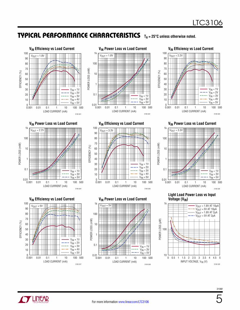
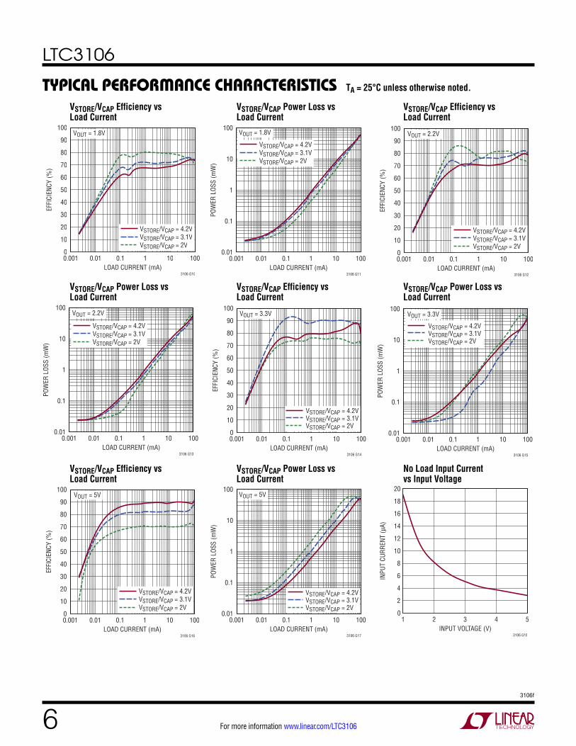
Typical perForMance characTerisTics
VIN Power Loss vs Load Current VIN Efficiency vs Load Current VIN Power Loss vs Load Current
VIN Efficiency vs Load Current VIN Power Loss vs Load CurrentLight Load Power Loss vs Input Voltage (VIN)
VIN Efficiency vs Load Current VIN Power Loss vs Load Current VIN Efficiency vs Load Current
TA = 25°C unless otherwise noted.
VOUT = 1.8V
VIN = 1VVIN = 2VVIN = 3VVIN = 4VVIN = 5V
LOAD CURRENT (mA)0.001 0.01 0.1 1 10 100 5000
10
20
30
40
50
60
70
80
90
100
EFFI
CIEN
CY (%
)
3106 G01
VOUT = 1.8V
VIN = 1VVIN = 3VVIN = 5V
LOAD CURRENT (mA)0.001 0.01 0.1 1 10 100 500
0.01
0.1
1
10
100
1k
POW
ER L
OSS
(mW
)
3106 G02
VOUT = 2.2V
LOAD CURRENT (mA)0.001 0.01 0.1 1 10 100 5000
10
20
30
40
50
60
70
80
90
100
EFFI
CIEN
CY (%
)
3106 G03
VIN = 1VVIN = 2VVIN = 3VVIN = 4VVIN = 5V
VOUT = 2.2V
LOAD CURRENT (mA)0.001 0.01 0.1 1 10 100 500
0.01
0.1
1
10
100
1k
POW
ER L
OSS
(mW
)
3106 G04
VIN = 1VVIN = 3VVIN = 5V
VOUT = 3.3V
LOAD CURRENT (mA)0.001 0.01 0.1 1 10 100 5000
10
20
30
40
50
60
70
80
90
100
EFFI
CIEN
CY (%
)
3106 G05
VIN = 1VVIN = 2VVIN = 3VVIN = 4VVIN = 5V
VOUT = 3.3V
LOAD CURRENT (mA)0.001 0.01 0.1 1 10 100 500
0.01
0.1
1
10
100
1k
POW
ER L
OSS
(mW
)
3106 G06
VIN = 1VVIN = 3VVIN = 5V
VOUT = 5V
LOAD CURRENT (mA)0.001 0.01 0.1 1 10 100 5000
10
20
30
40
50
60
70
80
90
100
EFFI
CIEN
CY (%
)
vs Load Current
3106 G07
VIN = 1VVIN = 2VVIN = 3VVIN = 4VVIN = 5V
VOUT = 5V
LOAD CURRENT (mA)0.001 0.01 0.1 1 10 100 500
0.01
0.1
1
10
100
1k
POW
ER L
OSS
(mW
)
3106 G08
VIN = 1VVIN = 3VVIN = 5V
VOUT = 1.8V AT 10µAVOUT = 5V AT 10µAVOUT = 1.8V AT 2µAVOUT = 5V AT 2µA
INPUT VOLTAGE, VIN (V)0 0.5 1 1.5 2 2.5 3 3.5 4 4.5 5
10
100
1k
POW
ER L
OSS
(µW
)
3106 G09
LTC3106
63106f
For more information www.linear.com/LTC3106
Typical perForMance characTerisTics TA = 25°C unless otherwise noted.
VSTORE/VCAP Power Loss vs Load Current
VSTORE/VCAP Efficiency vs Load Current
VSTORE/VCAP Power Loss vs Load Current
VSTORE/VCAP Efficiency vs Load Current
VSTORE/VCAP Power Loss vs Load Current
No Load Input Current vs Input Voltage
VSTORE/VCAP Efficiency vs Load Current
VSTORE/VCAP Power Loss vs Load Current
VSTORE/VCAP Efficiency vs Load Current
VOUT = 1.8V
VSTORE/VCAP = 4.2VVSTORE/VCAP = 3.1VVSTORE/VCAP = 2V
LOAD CURRENT (mA)0.001 0.01 0.1 1 10 1000
10
20
30
40
50
60
70
80
90
100
EFFI
CIEN
CY (%
)
3106 G10
VOUT = 1.8V
LOAD CURRENT (mA)0.001 0.01 0.1 1 10 100
0.01
0.1
1
10
100
POW
ER L
OSS
(mW
)
3106 G11
VSTORE/VCAP = 4.2VVSTORE/VCAP = 3.1VVSTORE/VCAP = 2V
VOUT = 2.2V
LOAD CURRENT (mA)0.001 0.01 0.1 1 10 1000
10
20
30
40
50
60
70
80
90
100
EFFI
CIEN
CY (%
)
3106 G12
VSTORE/VCAP = 4.2VVSTORE/VCAP = 3.1VVSTORE/VCAP = 2V
VOUT = 2.2V
LOAD CURRENT (mA)0.001 0.01 0.1 1 10 100
0.01
0.1
1
10
100
POW
ER L
OSS
(mW
)
3106 G13
VSTORE/VCAP = 4.2VVSTORE/VCAP = 3.1VVSTORE/VCAP = 2V
VOUT = 3.3V
VSTORE/VCAP = 4.2VVSTORE/VCAP = 3.1VVSTORE/VCAP = 2V
LOAD CURRENT (mA)0.001 0.01 0.1 1 10 1000
10
20
30
40
50
60
70
80
90
100
EFFI
CIEN
CY (%
)
3106 G14
VOUT = 3.3V
VSTORE/VCAP = 4.2VVSTORE/VCAP = 3.1VVSTORE/VCAP = 2V
LOAD CURRENT (mA)0.001 0.01 0.1 1 10 100
0.01
0.1
1
10
100
POW
ER L
OSS
(mW
)
3106 G15
VOUT = 5V
LOAD CURRENT (mA)0.001 0.01 0.1 1 10 1000
10
20
30
40
50
60
70
80
90
100
EFFI
CIEN
CY (%
)
3106 G16
VSTORE/VCAP = 4.2VVSTORE/VCAP = 3.1VVSTORE/VCAP = 2V
VOUT = 5V
/VVSTORE CAP = 4.2VVSTORE/VCAP = 3.1VVSTORE/VCAP = 2V
LOAD CURRENT (mA)0.001 0.01 0.1 1 10 100
0.01
0.1
1
10
100
POW
ER L
OSS
(mW
)
3106 G17
INPUT VOLTAGE (V)1 2 3 4 5
0
2
4
6
8
10
12
14
16
18
20
INPU
T CU
RREN
T (µ
A)
3106 G18
LTC3106
73106f
For more information www.linear.com/LTC3106
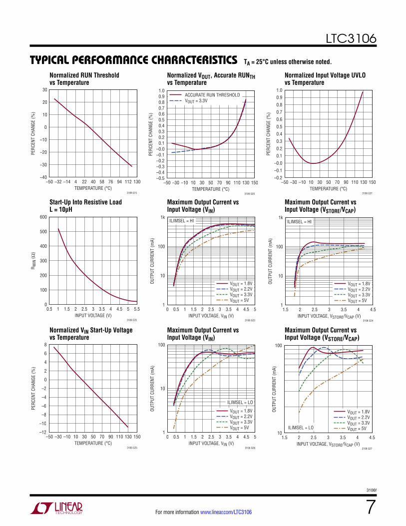
Maximum Output Current vs Input Voltage (VIN)
Maximum Output Current vs Input Voltage (VSTORE/VCAP)
Normalized VIN Start-Up Voltage vs Temperature
Maximum Output Current vs Input Voltage (VIN)
Maximum Output Current vs Input Voltage (VSTORE/VCAP)
Normalized VOUT, Accurate RUNTH vs Temperature
Normalized Input Voltage UVLO vs Temperature
Typical perForMance characTerisTics TA = 25°C unless otherwise noted.
TEMPERATURE (°C)–50 –32 –14 4 22 40 58 76 94 112 130
–40
–30
–20
–10
0
10
20
30
PERC
ENT
CHAN
GE (%
)
3106 G19
ACCURATE RUN THRESHOLDVOUT = 3.3V
TEMPERATURE (°C)–50 –30 –10 10 30 50 70 90 110 130 150
–0.5–0.4–0.3–0.2–0.1–0.00.10.20.30.40.50.60.70.80.91.0
PERC
ENT
CHAN
GE (%
)
3106 G20
TEMPERATURE (°C)–50 –30 –10 10 30 50 70 90 110 130 150
–0.2
–0.1
–0.0
0.1
0.2
0.3
0.4
0.5
0.6
0.7
0.8
0.9
1.0
PERC
ENT
CHAN
GE (%
)
3106 G21
INPUT VOLTAGE (V)0.5 1 1.5 2 2.5 3 3.5 4 4.5 5 5.5
0
100
200
300
400
500
600
R MIN
(Ω)
3106 G22
ILIMSEL = HI
VOUT = 1.8VVOUT = 2.2VVOUT = 3.3VVOUT = 5V
INPUT VOLTAGE, VIN (V)0 0.5 1 1.5 2 2.5 3 3.5 4 4.5 5
1
10
100
1k
OUTP
UT C
URRE
NT (m
A)
3106 G23
ILIMSEL = HI
INPUT VOLTAGE, VSTORE/VCAP (V)1.5 2 2.5 3 3.5 4 4.5
1
10
100
1k
OUTP
UT C
URRE
NT (m
A)
3106 G24
VOUT = 1.8VVOUT = 2.2VVOUT = 3.3VVOUT = 5V
TEMPERATURE (°C)–50 –30 –10 10 30 50 70 90 110 130 150
–12
–10
–8
–6
–4
–2
0
2
4
6
8
PERC
ENT
CHAN
GE (%
)
3106 G25
ILIMSEL = LO
INPUT VOLTAGE, VIN (V)0 0.5 1 1.5 2 2.5 3 3.5 4 4.5 5
1
10
100
OUTP
UT C
URRE
NT (m
A)
3106 G26
VOUT = 1.8VVOUT = 2.2VVOUT = 3.3VVOUT = 5V
Normalized RUN Threshold vs Temperature
Start-Up Into Resistive Load L = 10µH
ILIMSEL = LO
INPUT VOLTAGE, VSTORE/VCAP (V)1.5 2 2.5 3 3.5 4 4.5
10
100
OUTP
UT C
URRE
NT (m
A)
3106 G27
VOUT = 1.8VVOUT = 2.2VVOUT = 3.3VVOUT = 5V
LTC3106
83106f
For more information www.linear.com/LTC3106
No Load Input Current vs Input Voltage, MPP Enabled
5VIN to 3.3VOUT Load Step 10mA to 300mA
5VIN to 3.3VOUT Load Step 100µA to 40mA
Boost Mode at VIN = 1.5V VOUT = 3.3V, 100mA
Buck-Boost Mode at VIN = 3.5V VOUT = 3.3V 100mA
Buck Mode at VIN = 4.3V VOUT = 3.3V, 100mA
Typical perForMance characTerisTics TA = 25°C unless otherwise noted.
L = 10µH COUT = 100µFCOUT = 47µF
LOAD CURRENT (mA)0.001 0.01 0.1 1 10 100 500
–3.0
–2.5
–2.0
–1.5
–1.0
–0.5
0
0.5
1.0
LOAD
REG
ULAT
ION
(%)
3106 G28
COUT = 47µFILIMSEL = HI
100µs/DIV
IL200mA/DIV
ILOAD100mA/DIV
3106 G29
TEMPERATURE (°C)–50 –30 –10 10 30 50 70 90 110 130 150
–4
–3
–2
–1
0
1
PERC
ENT
CHAN
GE F
ROM
25°
C (%
)
3106 G30
INPUT VOLTAGE (V)0.4 1.3 2.2 3.2 4.1 5
0
100
200
300
400
500
600
700
INPU
T CU
RREN
T (µ
A)
3106 G31
Normalized Output Voltage Regulation vs Load Current Inductor Current vs Load Current
Normalized MPP Output vs Temperature
ILIMSEL = HI
COUT = 47µF
COUT = 100µF
1ms/DIV
VOUT200mV/DIV
ILOAD200mA/DIV
VOUT200mA/DIV
3106 G32
10mA
300mA
COUT = 47µF, ILIMSEL = LO
5ms/DIV
VOUT100mV/DIV
ILOAD20mA/DIV
3106 G33
40mA
100µA 100µA
L = 10µHCOUT = 47µFILIMSEL = HI
50µs/DIV
VOUT50mV/DIV
VAUX50mV/DIV
IL200mA/DIV
3106 G34
L = 10µHCOUT = 47µFILIMSEL = HI
50µs/DIV
VOUT100mV/DIV
VAUX20mV/DIV
IL200mA/DIV
3106 G35
L = 10µHCOUT = 47µFILIMSEL = HI
50µs/DIV
VOUT100mV/DIV
VAUX50mV/DIV
IL400mA/DIV
3106 G36
LTC3106
93106f
For more information www.linear.com/LTC3106
3.3V Output Voltage Ripple vs Load Current (ILIMSEL High)
3.3V Output Voltage Ripple vs Load Current (ILIMSEL Low)
5V Output Voltage Ripple vs Load Current (ILIMSEL High)
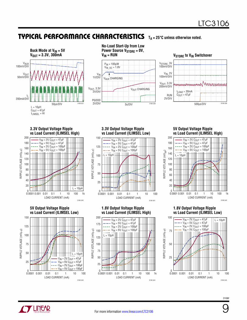
Buck Mode at VIN = 5V VOUT = 3.3V, 300mA
No-Load Start-Up from Low Power Source VSTORE = 0V, VIN = RUN
Typical perForMance characTerisTics TA = 25°C unless otherwise noted.
PIN = 100µWVIN_OC = 1.8V
VAUX CHARGING
VOUT CHARGING
5s/DIV
VOUT, 3.3V2V/DIV
VIN1V/DIV
PGOOD2V/DIV 3106 G38
ILOAD = 30mACOUT = 47µF
500µs/DIV
VOUT, 3.3V200mV/DIV
VSTORE, 3V100mV/DIV
VIN, 2V100mV/DIV
RUN2V/DIV
3106 G39
L = 10µH
VIN = 2V, COUT = 47µFVIN = 5V, COUT = 47µFVIN = 2V, COUT = 100µFVIN = 5V, COUT = 100µF
LOAD CURRENT (mA)0.0001 0.001 0.01 0.1 1 10 100 1k0
20
40
60
80
100
120
140
160
180
200
RIPP
LE V
OTLA
GE (m
V P-P
)
3106 G40
L = 10µH
LOAD CURRENT (mA)0.0001 0.001 0.01 0.1 1 10 1000
25
50
75
100
125
150
RIPP
LE V
OTLA
GE (m
V P-P
)
3106 G41
VIN = 2V, COUT = 47µFVIN = 5V, COUT = 47µFVIN = 2V, COUT = 100µFVIN = 5V, COUT = 100µF
L = 10µH
LOAD CURRENT (mA)0.0001 0.001 0.01 0.1 1 10 100 1k0
20
40
60
80
100
120
140
160
180
200
RIPP
LE V
OTLA
GE (m
V pp)
3106 G42
VIN = 2V, COUT = 47µFVIN = 5V, COUT = 47µFVIN = 2V, COUT = 100µFVIN = 5V, COUT = 100µF
L = 10µH
LOAD CURRENT (mA)0.0001 0.001 0.01 0.1 1 10 1000
25
50
75
100
125
150
RIPP
LE V
OTLA
GE (m
V P-P
)
3106 G43
VIN = 2V, COUT = 47µFVIN = 5V, COUT = 47µFVIN = 2V, COUT = 100µFVIN = 5V, COUT = 100µF
L = 10µH
LOAD CURRENT (mA)0.0001 0.001 0.01 0.1 1 10 100 1k0
25
50
75
100
125
150
175
200
RIPP
LE V
OTLA
GE (m
V P-P
)
3106 G44
VIN = 2V, COUT = 47µFVIN = 5V, COUT = 47µFVIN = 2V, COUT = 100µFVIN = 5V, COUT = 100µF
L = 10µH
LOAD CURRENT (mA)0.0001 0.001 0.01 0.1 1 10 1000
25
50
75
100
RIPP
LE V
OTLA
GE (m
V P-P
)
3106 G45
VIN = 2V, COUT = 47µFVIN = 5V, COUT = 47µFVIN = 2V, COUT = 100µFVIN = 5V, COUT = 100µF
VSTORE to VIN Switchover
5V Output Voltage Ripple vs Load Current (ILIMSEL Low)
1.8V Output Voltage Ripple vs Load Current (ILIMSEL High)
1.8V Output Voltage Ripple vs Load Current (ILIMSEL Low)
L = 10µHCOUT = 47µFILIMSEL = HI
50µs/DIV
VOUT50mV/DIV
VAUX100mV/DIV
IL200mA/DIV
3106 G37
LTC3106
103106f
For more information www.linear.com/LTC3106
Typical perForMance characTerisTics TA = 25°C unless otherwise noted.
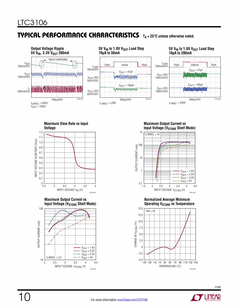
5V VIN to 1.8V VOUT Load Step 10µA to 50mA
5V VIN to 1.8V VOUT Load Step 10µA to 200mA
Output Voltage Ripple 5V VIN, 3.3V VOUT 200mA
Maximum Slew Rate vs Input Voltage
Maximum Output Current vs Input Voltage (VSTORE Shelf Mode)
Normalized Average Minimum Operating VSTORE vs Temperature
Maximum Output Current vs Input Voltage (VSTORE Shelf Mode)
INPUT VOLTAGE VIN (V)2.5 3 3.5 4 4.5 5
0
0.1
0.2
0.4
0.5
0.6
0.7
0.8
1.0
1.1
1.2
INPU
T VO
LTAG
E SL
EW R
ATE
(V/µ
s)
3106 G49
ILIMSEL = LO
INPUT VOLTAGE, VSTORE (V)2 2.5 3 3.5 4 4.5
10
100
OUTP
UT C
URRE
NT (m
A)
3106 G51
VOUT = 1.8VVOUT = 2.2VVOUT = 3.3VVOUT = 5V
PRI = HI
TEMPERATURE (°C)–50 –30 –10 10 30 50 70 90 110 130 150
–5.0
–2.5
0
2.5
5.0
7.5
10.0
12.5
15.0
CHAN
GE IN
VST
ORE
(%)
3106 G52
ILIMSEL = HI
INPUT VOLTAGE, VSTORE (V)1.5 2 2.5 3 3.5 4 4.5
0.1
1
10
100
1kOU
TPUT
CUR
RENT
(mA)
3106 G50
VOUT = 1.8VVOUT = 2.2VVOUT = 3.3VVOUT = 5V
ILIMSEL = HIGHCOUT = 100µF
100µs/DIV
IL500mA/DIV
VOUT100mV/DIV
VAUX100mV/DIV
3106 G46
VAUX CHARGING
ILIMSEL = LOW
COUT = 47µF
COUT = 100µF
10µA 10µA50mA
500µs/DIV
ILOAD50mA/DIV
VOUT (AC)50mV/DIV
VOUT (AC)50mV/DIV
3106 G47
ILIMSEL = HIGH
COUT = 47µF
COUT = 100µF
10µA 10µA200mA
500µs/DIV
ILOAD200mA/DIV
100mV/DIV
VOUT (AC)
VOUT (AC)
100mV/DIV
3106 G48
LTC3106
113106f
For more information www.linear.com/LTC3106
pin FuncTions (QFN/TSSOP)
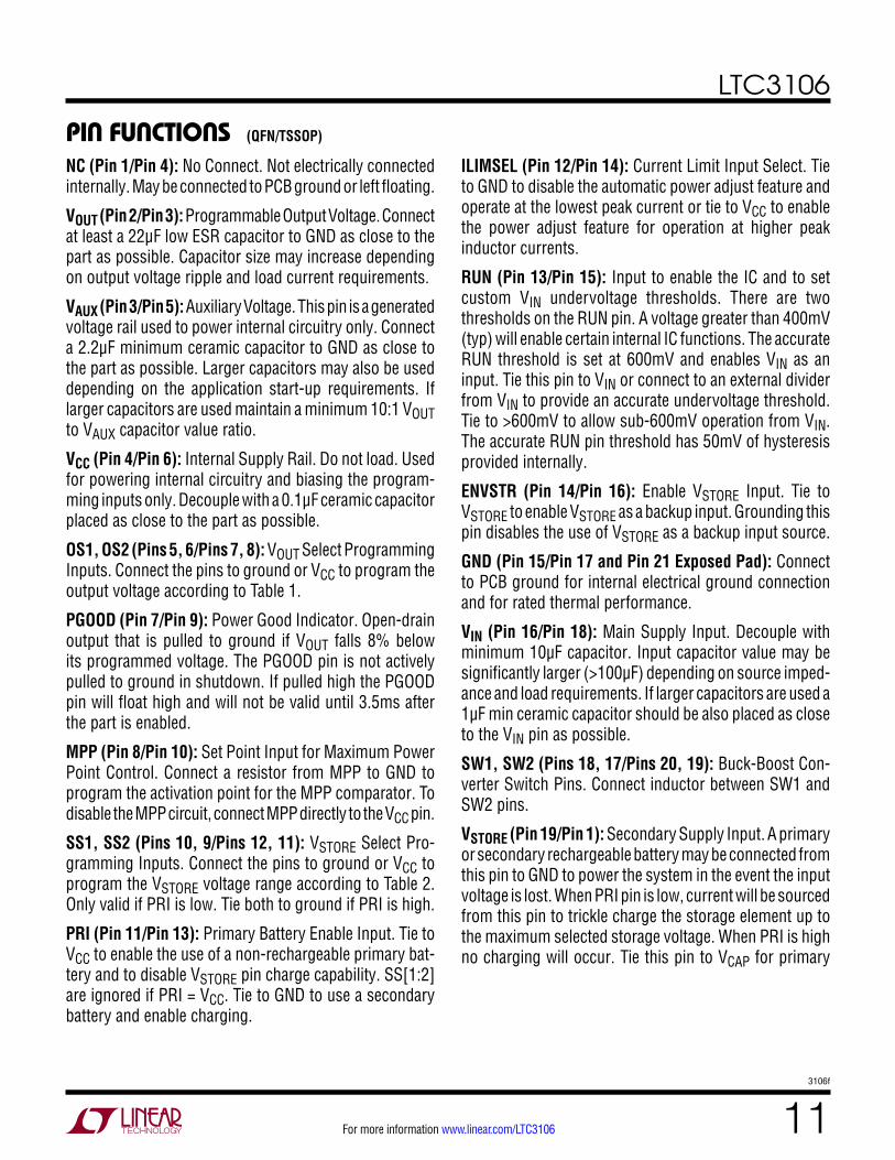
NC (Pin 1/Pin 4): No Connect. Not electrically connected internally. May be connected to PCB ground or left floating.
VOUT (Pin 2/Pin 3): Programmable Output Voltage. Connect at least a 22μF low ESR capacitor to GND as close to the part as possible. Capacitor size may increase depending on output voltage ripple and load current requirements.
VAUX (Pin 3/Pin 5): Auxiliary Voltage. This pin is a generated voltage rail used to power internal circuitry only. Connect a 2.2μF minimum ceramic capacitor to GND as close to the part as possible. Larger capacitors may also be used depending on the application start-up requirements. If larger capacitors are used maintain a minimum 10:1 VOUT to VAUX capacitor value ratio.
VCC (Pin 4/Pin 6): Internal Supply Rail. Do not load. Used for powering internal circuitry and biasing the program-ming inputs only. Decouple with a 0.1μF ceramic capacitor placed as close to the part as possible.
OS1, OS2 (Pins 5, 6/Pins 7, 8): VOUT Select Programming Inputs. Connect the pins to ground or VCC to program the output voltage according to Table 1.
PGOOD (Pin 7/Pin 9): Power Good Indicator. Open-drain output that is pulled to ground if VOUT falls 8% below its programmed voltage. The PGOOD pin is not actively pulled to ground in shutdown. If pulled high the PGOOD pin will float high and will not be valid until 3.5ms after the part is enabled.
MPP (Pin 8/Pin 10): Set Point Input for Maximum Power Point Control. Connect a resistor from MPP to GND to program the activation point for the MPP comparator. To disable the MPP circuit, connect MPP directly to the VCC pin.
SS1, SS2 (Pins 10, 9/Pins 12, 11): VSTORE Select Pro-gramming Inputs. Connect the pins to ground or VCC to program the VSTORE voltage range according to Table 2. Only valid if PRI is low. Tie both to ground if PRI is high.
PRI (Pin 11/Pin 13): Primary Battery Enable Input. Tie to VCC to enable the use of a non-rechargeable primary bat-tery and to disable VSTORE pin charge capability. SS[1:2] are ignored if PRI = VCC. Tie to GND to use a secondary battery and enable charging.
ILIMSEL (Pin 12/Pin 14): Current Limit Input Select. Tie to GND to disable the automatic power adjust feature and operate at the lowest peak current or tie to VCC to enable the power adjust feature for operation at higher peak inductor currents.
RUN (Pin 13/Pin 15): Input to enable the IC and to set custom VIN undervoltage thresholds. There are two thresholds on the RUN pin. A voltage greater than 400mV (typ) will enable certain internal IC functions. The accurate RUN threshold is set at 600mV and enables VIN as an input. Tie this pin to VIN or connect to an external divider from VIN to provide an accurate undervoltage threshold. Tie to >600mV to allow sub-600mV operation from VIN. The accurate RUN pin threshold has 50mV of hysteresis provided internally.
ENVSTR (Pin 14/Pin 16): Enable VSTORE Input. Tie to VSTORE to enable VSTORE as a backup input. Grounding this pin disables the use of VSTORE as a backup input source.
GND (Pin 15/Pin 17 and Pin 21 Exposed Pad): Connect to PCB ground for internal electrical ground connection and for rated thermal performance.
VIN (Pin 16/Pin 18): Main Supply Input. Decouple with minimum 10µF capacitor. Input capacitor value may be significantly larger (>100µF) depending on source imped-ance and load requirements. If larger capacitors are used a 1µF min ceramic capacitor should be also placed as close to the VIN pin as possible.
SW1, SW2 (Pins 18, 17/Pins 20, 19): Buck-Boost Con-verter Switch Pins. Connect inductor between SW1 and SW2 pins.
VSTORE (Pin 19/Pin 1): Secondary Supply Input. A primary or secondary rechargeable battery may be connected from this pin to GND to power the system in the event the input voltage is lost. When PRI pin is low, current will be sourced from this pin to trickle charge the storage element up to the maximum selected storage voltage. When PRI is high no charging will occur. Tie this pin to VCAP for primary
LTC3106
123106f
For more information www.linear.com/LTC3106
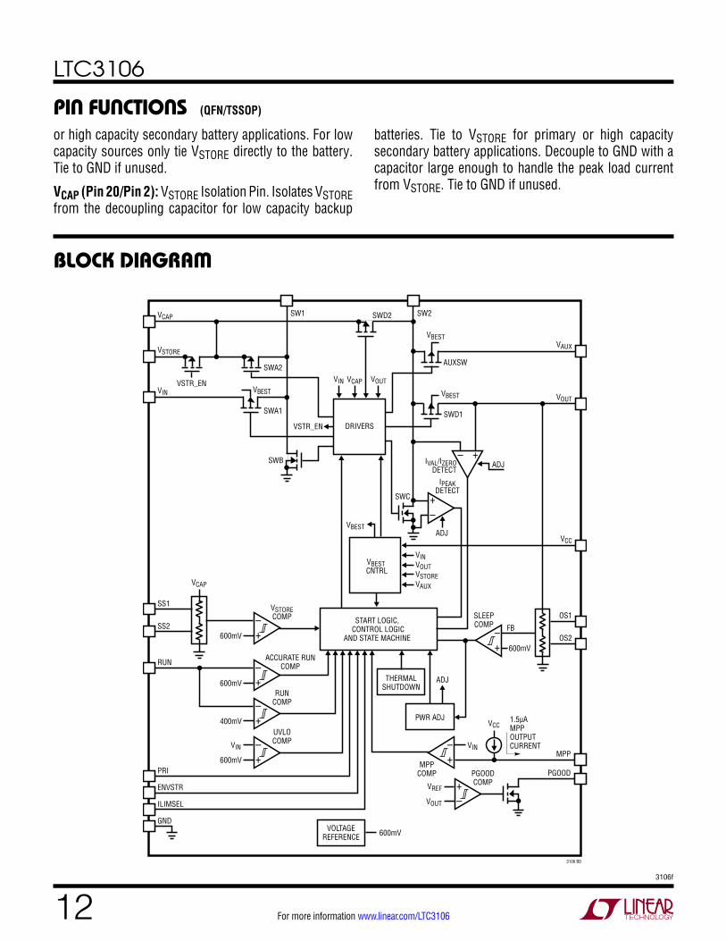
block DiagraM
+–
START LOGIC, CONTROL LOGIC
AND STATE MACHINE
VBEST CNTRL
THERMALSHUTDOWN
VSTORECOMP
VCAP
SS1
VIN
VSTORE
VCAP
SS2
RUN
PRI
ENVSTR
ILIMSEL
GND
600mV
600mV
400mV
600mV
VOLTAGEREFERENCE
PWR ADJ
+–
+–
UVLOCOMP
600mV
VIN
600mV
FB
1.5µAMPPOUTPUTCURRENT
VCC
ADJ
MPP
OS2
OS1
VOUT
VIN
+–
PGOODCOMP
MPPCOMP
VOUT
VREF
+–
RUNCOMP
SLEEPCOMP
+– ACCURATE RUN
COMP
VCC
VBEST
SWD1
SWB
SWA1
VSTR_EN
VOUT
VAUX
SWA2
VSTR_ENVBEST
SWD2
VBEST
VCAPVIN VOUT
AUXSW
PGOOD
3106 BD
+–
VIN
ADJ
IPEAKDETECT
IVAL/IZERODETECT
ADJ
VAUX
VSTORE
DRIVERS
+–
+–
SW1 SW2
VBEST
SWC
or high capacity secondary battery applications. For low capacity sources only tie VSTORE directly to the battery. Tie to GND if unused.
VCAP (Pin 20/Pin 2): VSTORE Isolation Pin. Isolates VSTORE from the decoupling capacitor for low capacity backup
batteries. Tie to VSTORE for primary or high capacity secondary battery applications. Decouple to GND with a capacitor large enough to handle the peak load current from VSTORE. Tie to GND if unused.
pin FuncTions (QFN/TSSOP)
LTC3106
133106f
For more information www.linear.com/LTC3106
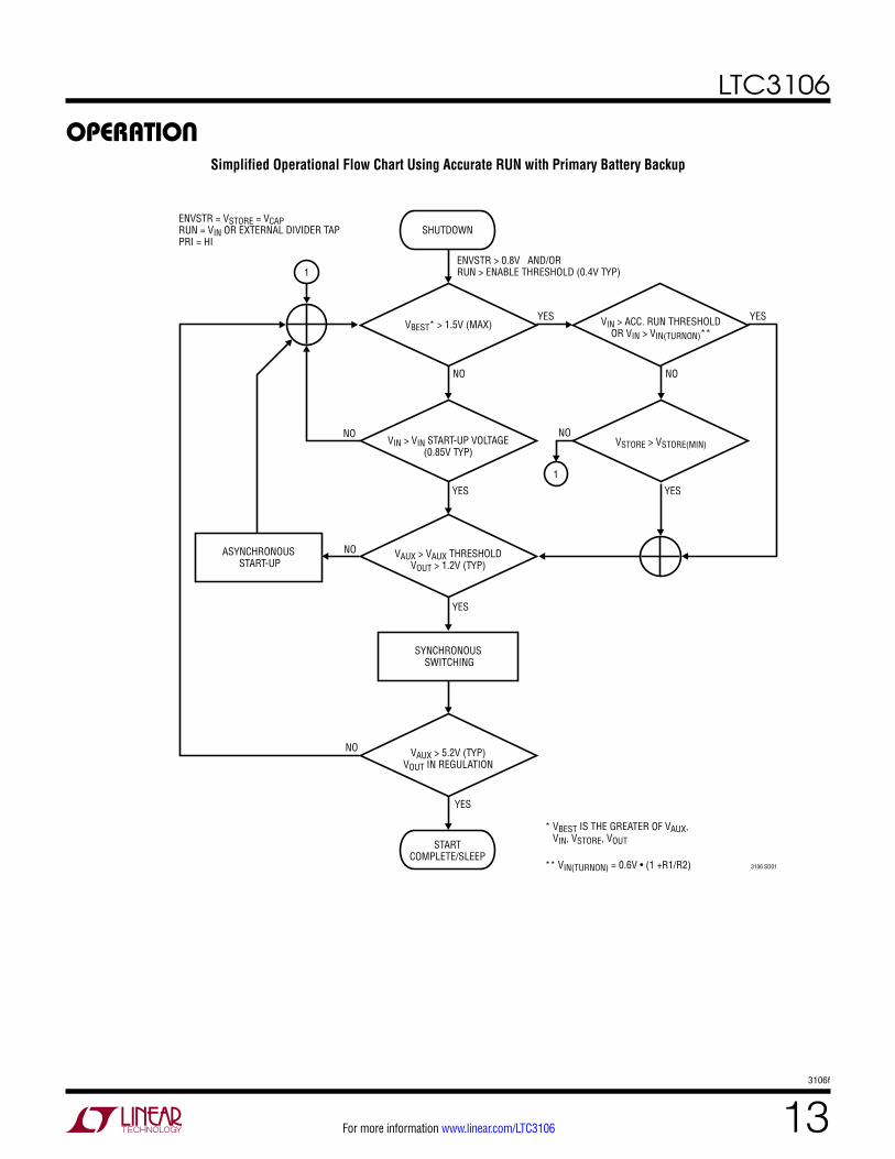
Simplified Operational Flow Chart Using Accurate RUN with Primary Battery Backup
operaTion
3106 SD01
VBEST* > 1.5V (MAX)
VIN > VIN START-UP VOLTAGE(0.85V TYP)
ENVSTR > 0.8V AND/ORRUN > ENABLE THRESHOLD (0.4V TYP)
ENVSTR = VSTORE = VCAPRUN = VIN OR EXTERNAL DIVIDER TAPPRI = HI
VAUX > VAUX THRESHOLDVOUT > 1.2V (TYP)
* VBEST IS THE GREATER OF VAUX, VIN, VSTORE, VOUT
** VIN(TURNON) = 0.6V • (1 +R1/R2)
SYNCHRONOUS SWITCHING
VSTORE > VSTORE(MIN)
YES YES
NO
VIN > ACC. RUN THRESHOLDOR VIN > VIN(TURNON)**
ASYNCHRONOUS START-UP
SHUTDOWN
NO
NO
1
STARTCOMPLETE/SLEEP
YESYES
YES
NO
VAUX > 5.2V (TYP)VOUT IN REGULATION
NO
YES
NO
1
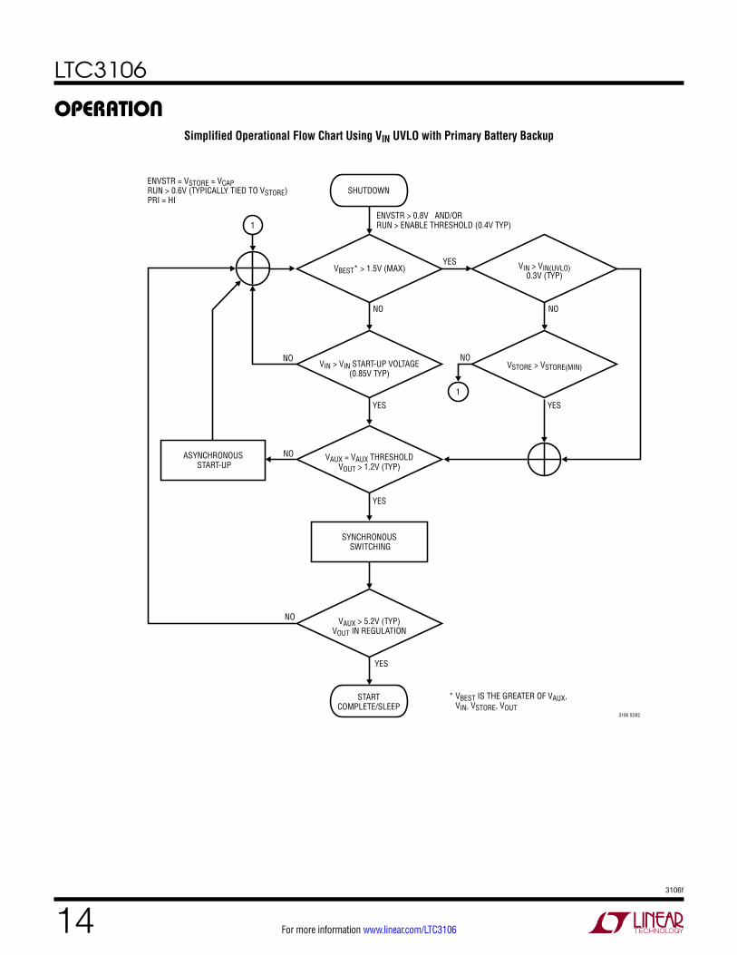
LTC3106
143106f
For more information www.linear.com/LTC3106
Simplified Operational Flow Chart Using VIN UVLO with Primary Battery Backup
operaTion
3106 SD02
VBEST* > 1.5V (MAX)
VIN > VIN START-UP VOLTAGE(0.85V TYP)
ENVSTR > 0.8V AND/ORRUN > ENABLE THRESHOLD (0.4V TYP)
ENVSTR = VSTORE = VCAPRUN > 0.6V (TYPICALLY TIED TO VSTORE)PRI = HI
VAUX = VAUX THRESHOLDVOUT > 1.2V (TYP)
* VBEST IS THE GREATER OF VAUX, VIN, VSTORE, VOUT
SYNCHRONOUS SWITCHING
VSTORE > VSTORE(MIN)
YES
NO
VIN > VIN(UVLO)0.3V (TYP)
ASYNCHRONOUS START-UP
SHUTDOWN
NO
NO
1
STARTCOMPLETE/SLEEP
YESYES
YES
NO
VAUX > 5.2V (TYP)VOUT IN REGULATION
NO
YES
NO
1
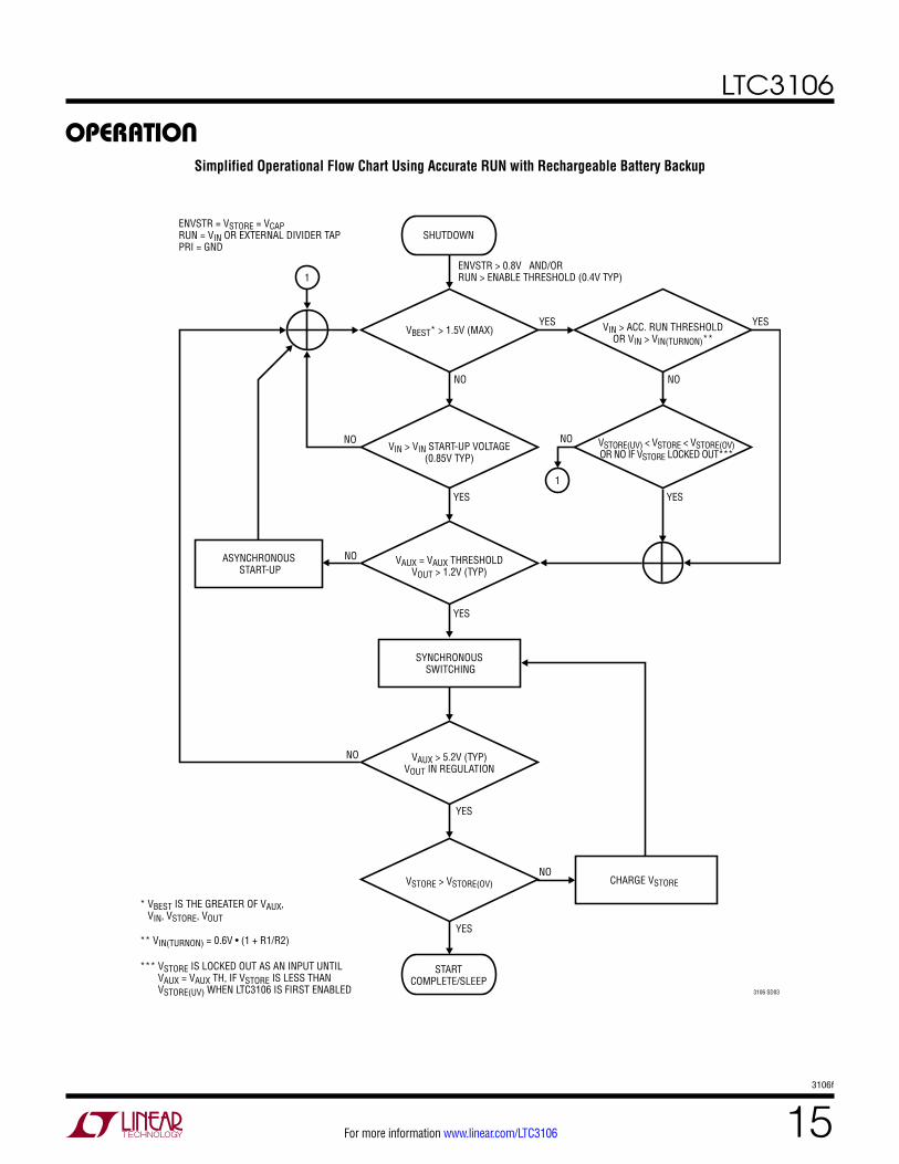
LTC3106
153106f
For more information www.linear.com/LTC3106
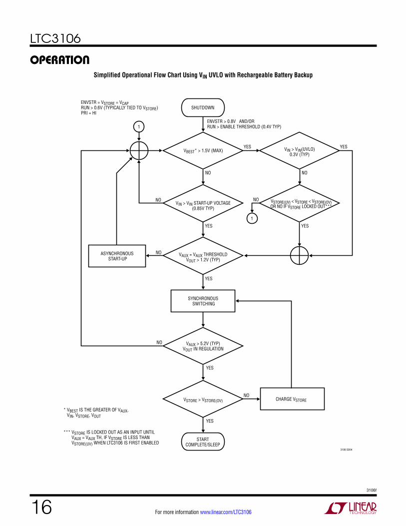
operaTionSimplified Operational Flow Chart Using Accurate RUN with Rechargeable Battery Backup
3106 SD03
VBEST* > 1.5V (MAX)
VIN > VIN START-UP VOLTAGE(0.85V TYP)
ENVSTR > 0.8V AND/ORRUN > ENABLE THRESHOLD (0.4V TYP)
ENVSTR = VSTORE = VCAPRUN = VIN OR EXTERNAL DIVIDER TAPPRI = GND
VAUX = VAUX THRESHOLDVOUT > 1.2V (TYP)
* VBEST IS THE GREATER OF VAUX, VIN, VSTORE, VOUT
** VIN(TURNON) = 0.6V • (1 + R1/R2)
*** VSTORE IS LOCKED OUT AS AN INPUT UNTIL VAUX = VAUX TH, IF VSTORE IS LESS THAN VSTORE(UV) WHEN LTC3106 IS FIRST ENABLED
SYNCHRONOUS SWITCHING
VSTORE(UV) < VSTORE < VSTORE(OV)OR NO IF VSTORE LOCKED OUT***
YES YES
NO
VIN > ACC. RUN THRESHOLDOR VIN > VIN(TURNON)**
CHARGE VSTORE
ASYNCHRONOUS START-UP
SHUTDOWN
NO
NO
1
STARTCOMPLETE/SLEEP
YESYES
YES
NO
VAUX > 5.2V (TYP)VOUT IN REGULATION
NO
YES
YES
VSTORE > VSTORE(OV)
NO
1
NO
LTC3106
163106f
For more information www.linear.com/LTC3106
operaTion
3106 SD04
VBEST* > 1.5V (MAX)
VIN > VIN START-UP VOLTAGE(0.85V TYP)
ENVSTR > 0.8V AND/ORRUN > ENABLE THRESHOLD (0.4V TYP)
ENVSTR = VSTORE = VCAPRUN > 0.6V (TYPICALLY TIED TO VSTORE)PRI = HI
VAUX = VAUX THRESHOLDVOUT > 1.2V (TYP)
* VBEST IS THE GREATER OF VAUX, VIN, VSTORE, VOUT
*** VSTORE IS LOCKED OUT AS AN INPUT UNTIL VAUX = VAUX TH, IF VSTORE IS LESS THAN VSTORE(UV) WHEN LTC3106 IS FIRST ENABLED
SYNCHRONOUS SWITCHING
VSTORE(UV) < VSTORE < VSTORE(OV)OR NO IF VSTORE LOCKED OUT***
YES YES
NO
VIN > VIN(UVLO)0.3V (TYP)
CHARGE VSTORE
ASYNCHRONOUS START-UP
SHUTDOWN
NO
NO
1
STARTCOMPLETE/SLEEP
YESYES
YES
NO
VAUX > 5.2V (TYP)VOUT IN REGULATION
NO
YES
YES
VSTORE > VSTORE(OV)
NO
1
NO
Simplified Operational Flow Chart Using VIN UVLO with Rechargeable Battery Backup
LTC3106
173106f
For more information www.linear.com/LTC3106
operaTionIntroduction
The LTC3106 is a high performance two input, synchro-nous buck-boost converter with low quiescent current over a wide input voltage range (refer to graph G18). The PowerPath control architecture allows the use of a single inductor to generate a user selectable fixed regulated output voltage through seamless transition between either of the two power inputs. If input power is available (VIN) or the backup battery is present (VSTORE), the buck-boost regulator will operate from VIN providing up to 300mA to the load. Should the VIN source become unavailable the regulator will select VSTORE/VCAP as its input delivering up to 90mA to the load. If a rechargeable battery is used as the backup source, a low current recharge power path is also provided allowing use of excess input energy to charge the backup source if the output voltage is in regulation. User selectable upper and lower thresholds are available to handle multiple battery chemistries and to protect the battery from overcharge/deep discharge. Charging can be externally disabled using the PRI pin for use of a primary battery as the backup source.
VIN
The main input voltage, VIN, can be configured to operate over an extended voltage range to accommodate multiple power source types including but not limited to high im-pedance sources. An accurate RUN pin allows predictable regulator turn-on at a specified input voltage. Optional maximum power point control (MPPC) capability is also integrated into the LTC3106. Either can be used to ensure maximum power extraction from non-ideal power sources.
VSTORE/VCAP
A backup source can be tied to VSTORE. As shown in the Block Diagram, VSTORE can be isolated from VCAP by the isolation switch for near zero current draw requirements and lower output current levels. When using the isolation feature the ILIMSEL pin should be tied to ground due to the increased series resistance the isolation switch adds.
For typical secondary and primary battery backup appli-cations isolation is not needed, VSTORE and VCAP should be shorted together. In this configuration the ILIMSEL feature can be used to increase output current to higher.
Both configurations are shown in Figure 1. In either con-figuration, VCAP is always enabled at start-up if ENVSTR is high to determine if VCAP is within the programmed voltage range. If VCAP is below the lower threshold it is latched off during start-up to minimize quiescent current draw from VCAP. Since the voltage on VCAP is continually monitored a very small 100nA typical quiescent current will persist with VCAP in shutdown (ENVSTR tied to GND).
Figure 1. VSTORE/VCAP Configurations
Shutdown
Either input source can be enabled independently or to-gether. Bring ENVSTR below the worst-case logic thresh-old of 0.3V to disable VSTORE/VCAP as input or output if charging is enabled (PRI low). Bringing ENVSTR below 0.3V will also turn off the isolation switch if the LTC3106 is configured to isolate VSTORE from VCAP.
A low voltage logic input on the RUN pin enables some circuit functions at 400mV typical while an accurate com-parator enables VIN as an input. To disable VIN as an input, RUN must be below the accurate RUN threshold of 600mV (typ). To put the LTC3106 in shutdown mode the ENVSTR pin must be below 0.3V and the RUN pin must be brought below the worst-case low level logic threshold of 150mV.
Accurate RUN Pin
If RUN is brought below the 500mV accurate comparator falling threshold, the buck-boost converter will inhibit switching from VIN. Certain control circuits will remain powered unless RUN is brought below its low level logic threshold of 400mV. A small amount of current draw on VIN will still remain in this mode.
VSTOREVCAP
ILIMSELBACKUPPOWER
VCC FOR IPEAK = 170mAGND FOR IPEAK = 100mA
LTC3106
NONISOLATEDVSTORE/VCAP
ISHDN = 100nA
VSTOREVCAP
ILIMSELBACKUPPOWER
LTC3106
ISOLATEDVSTORE/VCAP
ISHDN = 0.1nA IPEAK = 100mA
3106 F01
LTC3106
183106f
For more information www.linear.com/LTC3106
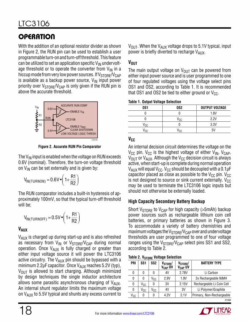
With the addition of an optional resistor divider as shown in Figure 2, the RUN pin can be used to establish a user programmable turn-on and turn-off threshold. This feature can be utilized to set an application specific VIN undervolt-age threshold or to operate the converter from VIN in a hiccup mode from very low power sources. If VSTORE/VCAP is available as a backup power source, VIN input power priority over VSTORE/VCAP is only given if the RUN pin is above the accurate threshold.
operaTionVOUT. When the VAUX voltage drops to 5.1V typical, input power is briefly diverted to recharge VAUX.
VOUT
The main output voltage on VOUT can be powered from either input power source and is user programmed to one of four regulated voltages using the voltage select pins OS1 and OS2, according to Table 1. It is recommended that OS1 and OS2 be tied to either ground or VCC.
Table 1. Output Voltage SelectionOS1 OS2 OUTPUT VOLTAGE
0 0 1.8V0 VCC 2.2V
VCC 0 3.3VVCC VCC 5V
VCC
An internal decision circuit determines the voltage on the VCC pin. VCC is the highest voltage of either VIN, VCAP, VOUT or VAUX. Although the VCC decision circuit is always active, when start-up is complete during normal operation VAUX will equal VCC. VCC should be decoupled with a 0.1µF capacitor placed as close as possible to the VCC pin. VCC is not designed to source or sink current externally. VCC may be used to terminate the LTC3106 logic inputs but should not otherwise be externally loaded.
High Capacity Secondary Battery Backup
Short VSTORE to VCAP for high capacity (>5mAh) backup power sources such as rechargeable lithium coin cell batteries, or primary batteries as shown in Figure 3. To accommodate a variety of battery chemistries and maximum voltages the VSTORE/VCAP over and undervoltage thresholds are user programmed to one of four voltage ranges using the VSTORE/VCAP select pins SS1 and SS2, according to Table 2.
Table 2. VSTORE Voltage SelectionPRI SS1 SS2 VSTORE/
VCAP OVVSTORE/VCAP UV
BATTERY TYPE
0 0 0 4V 2.78V Li Carbon0 0 VCC 2.9V 1.9V 2x Rechargeable NiMH0 VCC 0 3V 2.15V Rechargeable Li Coin Cell0 VCC VCC 4V 3V Li Polymer/Graphite
VCC 0 0 4.2V 2.1V Primary, Non-Rechargeable
VIN 0.6VENABLE VIN
ACCURATE RUN COMP
LTC3106
3106 F02
LOW VOLTAGE LOGIC THRESH
RUNR1
R2 ENABLE VREF,CLEAR SHUTDOWN0.4V
+–
+–
Figure 2. Accurate RUN Pin Comparator
The VIN input is enabled when the voltage on RUN exceeds 0.6V (nominal). Therefore, the turn-on voltage threshold on VIN can be set externally and is given by:
VIN(TURNON) = 0.6V • 1+ R1
R2
The RUN comparator includes a built-in hysteresis of ap-proximately 100mV, so that the typical turn-off threshold will be;
VIN(TURNOFF) = 0.5V • 1+ R1
R2
VAUX
VAUX is charged up during start-up and is also refreshed as necessary from VIN or VSTORE/VCAP during normal operation. Once VAUX is fully charged or greater than either input voltage source it will power the LTC3106 active circuitry. The VAUX pin should be bypassed with a minimum 2.2μF capacitor. Once VAUX reaches 5.2V (typ), VOUT is allowed to start charging. Although minimized by design techniques the single inductor architecture allows some parasitic asynchronous charging of VAUX. An internal shunt regulator limits the maximum voltage on VAUX to 5.5V typical and shunts any excess current to
LTC3106
193106f
For more information www.linear.com/LTC3106
operaTion
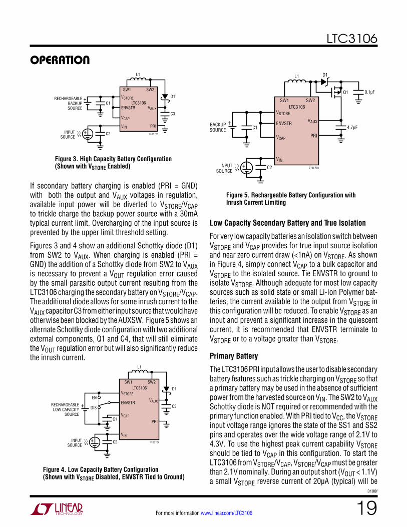
If secondary battery charging is enabled (PRI = GND) with both the output and VAUX voltages in regulation, available input power will be diverted to VSTORE/VCAP to trickle charge the backup power source with a 30mA typical current limit. Overcharging of the input source is prevented by the upper limit threshold setting.
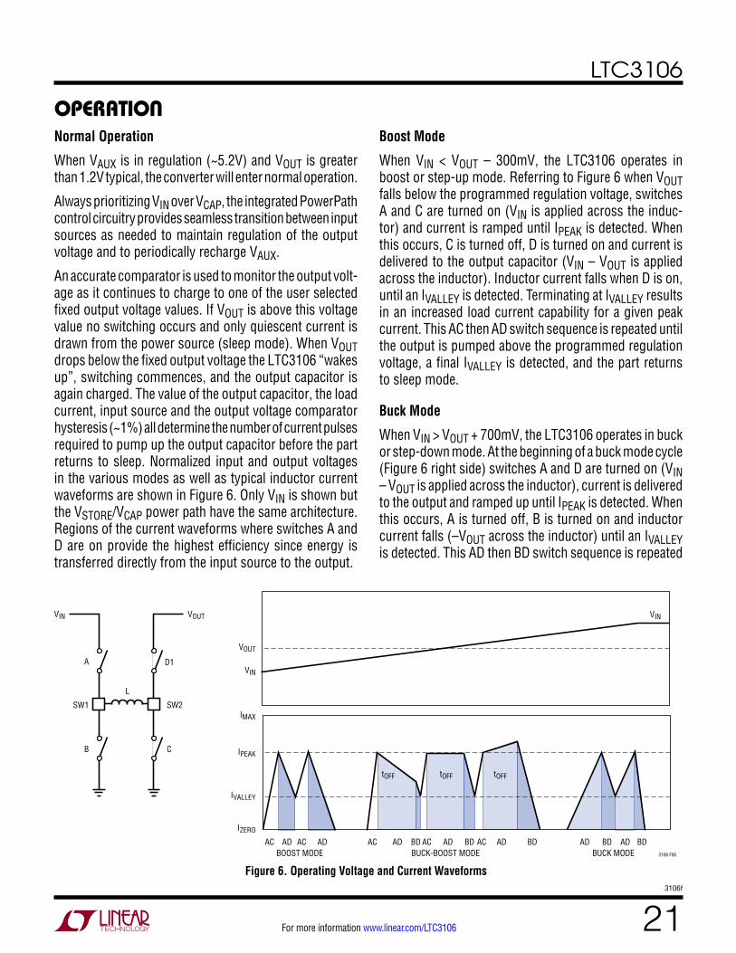
Figures 3 and 4 show an additional Schottky diode (D1) from SW2 to VAUX. When charging is enabled (PRI = GND) the addition of a Schottky diode from SW2 to VAUX is necessary to prevent a VOUT regulation error caused by the small parasitic output current resulting from the LTC3106 charging the secondary battery on VSTORE/VCAP. The additional diode allows for some inrush current to the VAUX capacitor C3 from either input source that would have otherwise been blocked by the AUXSW. Figure 5 shows an alternate Schottky diode configuration with two additional external components, Q1 and C4, that will still eliminate the VOUT regulation error but will also significantly reduce the inrush current.
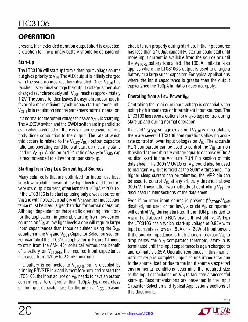
Low Capacity Secondary Battery and True Isolation
For very low capacity batteries an isolation switch between VSTORE and VCAP provides for true input source isolation and near zero current draw (<1nA) on VSTORE. As shown in Figure 4, simply connect VCAP to a bulk capacitor and VSTORE to the isolated source. Tie ENVSTR to ground to isolate VSTORE. Although adequate for most low capacity sources such as solid state or small Li-Ion Polymer bat-teries, the current available to the output from VSTORE in this configuration will be reduced. To enable VSTORE as an input and prevent a significant increase in the quiescent current, it is recommended that ENVSTR terminate to VSTORE or to a voltage greater than VSTORE.
Primary Battery
The LTC3106 PRI input allows the user to disable secondary battery features such as trickle charging on VSTORE so that a primary battery may be used in the absence of sufficient power from the harvested source on VIN. The SW2 to VAUX Schottky diode is NOT required or recommended with the primary function enabled. With PRI tied to VCC, the VSTORE input voltage range ignores the state of the SS1 and SS2 pins and operates over the wide voltage range of 2.1V to 4.3V. To use the highest peak current capability VSTORE should be tied to VCAP in this configuration. To start the LTC3106 from VSTORE/VCAP, VSTORE/VCAP must be greater than 2.1V nominally. During an output short (VOUT < 1.1V) a small VSTORE reverse current of 20µA (typical) will be
Figure 3. High Capacity Battery Configuration (Shown with VSTORE Enabled)
Figure 4. Low Capacity Battery Configuration (Shown with VSTORE Disabled, ENVSTR Tied to Ground)
Figure 5. Rechargeable Battery Configuration with Inrush Current Limiting
+
+INPUTSOURCE
RECHARGEABLEBACKUPSOURCE
LTC3106
VIN
VCAP
VAUX
PRI
SW1 SW2
VSTORE
ENVSTR
3106 F03
C1
C2
C3
D1
L1
+
+INPUTSOURCE
RECHARGEABLELOW CAPACITY
SOURCE
LTC3106
VIN
VCAP
VSTORE
ENVSTR
3106 F04
C1
EN
DIS
C2
VAUX
PRI
SW1 SW2
C3
D1
L1
+
+INPUTSOURCE
BACKUPSOURCE
LTC3106
VIN
VCAP
VSTORE
ENVSTR
3106 F05
C1
C2
VAUX
PRI
SW1 SW2
4.7µF
D1
Q1
L1
0.1µF
LTC3106
203106f
For more information www.linear.com/LTC3106
operaTionpresent. If an extended duration output short is expected, protection for the primary battery should be considered.
Start-Up
The LTC3106 will start up from either input voltage source but gives priority to VIN. The AUX output is initially charged with the synchronous rectifiers disabled. Once VAUX has reached its terminal voltage the output voltage is then also charged asynchronously until VOUT reaches approximately 1.2V. The converter then leaves the asynchronous mode in favor of a more efficient synchronous start-up mode until VOUT is in regulation and the part enters normal operation.
It is normal for the output voltage to rise as VAUX is charging. The AUXSW switch and the SWDI switch are in parallel so even when switched off there is still some asynchronous body diode conduction to the output. The rate at which this occurs is related to the VAUX/VOUT output capacitor ratio and operating conditions at start-up (i.e., any static load on VOUT). A minimum 10:1 ratio of VOUT to VAUX cap is recommended to allow for proper start-up.
Starting from Very Low Current Input Sources
Many solar cells that are optimized for indoor use have very low available power at low light levels and therefore very low output current, often less than 100µA at 200Lux. If the LTC3106 is to start up using only a weak source on VIN and with no back up battery on VSTORE the input capaci-tance must be sized larger than that for normal operation. Although dependent on the specific operating conditions for the application, in general, starting from low current sources on VIN at low light levels alone will require larger input capacitances than those calculated using the CVIN equation in the VIN and VOUT Capacitor Selection section. For example if the LTC3106 application in Figure 14 needs to start from the AM-1454 solar cell without the benefit of a battery on VSTORE, the required input capacitance increases from 470µF to 2.2mF minimum.
If a battery is connected to VSTORE but is disabled by bringing ENVSTR low and is therefore not used to start the LTC3106, the input source on VIN needs to have an output current equal to or greater than 100µA (typ) regardless of the input capacitor size for the internal VCC decision
circuit to run properly during start up. If the input source has less than a 100µA capability, startup could stall until more input current is available from the source or until the VSTORE battery is enabled. The 100µA limitation also applies where the LTC3106’s output is used to charge a battery or a large super capacitor. For typical applications where the input capacitance is greater than the output capacitance the 100µA limitation does not apply.
Operating from a Low Power VIN
Controlling the minimum input voltage is essential when using high impedance or intermittent input sources. The LTC3106 has several options for VIN voltage control during start-up and during normal operation.
If a valid VSTORE voltage exists or if VAUX is in regulation, there are several LTC3106 configurations allowing accu-rate control at lower input voltages on VIN. The accurate RUN comparator can be used to control the VIN turn-on threshold at any arbitrary voltage equal to or above 600mV as discussed in the Accurate RUN Pin section of this data sheet. The 300mV UVLO on VIN could also be used to maintain VIN but is fixed at the 300mV threshold. If a higher sleep current can be tolerated, the MPP pin can be used to control VIN at any arbitrary threshold above 300mV. These latter two methods of controlling VIN are discussed in later sections of the data sheet.
Even if no other input source is present (VSTORE/VCAP disabled, not used or too low), a crude VIN comparator will control VIN during start-up. If the RUN pin is tied to VIN or held above the RUN enable threshold (>0.4V typ) the LTC3106 has a typical start-up voltage of 0.85V with input currents as low as 15µA or ~12µW of input power. If the source impedance is high enough to cause VIN to drop below the VIN comparator threshold, start-up is terminated until the input capacitance is again charged to approximately 0.85V. Operation continues in this manner until start-up is complete. Input source impedance due to the source itself or due to the input source’s expected environmental conditions determine the required size of the input capacitance on VIN to facilitate a successful start-up. Recommendations are presented in the Input Capacitor Selection and Typical Applications sections of this document.
LTC3106
213106f
For more information www.linear.com/LTC3106
BOOST MODE BUCK-BOOST MODE BUCK MODE
VOUT
IMAX
IPEAK
IVALLEY
IZERO
VIN
VIN
tOFF tOFFtOFF
AC AC AC AD AD ADADAD AD AD ACAC BD BDBD BD BD3106 F06
VIN VOUT
A
B C
D1
SW1 SW2
L
Figure 6. Operating Voltage and Current Waveforms
operaTionNormal Operation
When VAUX is in regulation (~5.2V) and VOUT is greater than 1.2V typical, the converter will enter normal operation.
Always prioritizing VIN over VCAP, the integrated PowerPath control circuitry provides seamless transition between input sources as needed to maintain regulation of the output voltage and to periodically recharge VAUX.
An accurate comparator is used to monitor the output volt-age as it continues to charge to one of the user selected fixed output voltage values. If VOUT is above this voltage value no switching occurs and only quiescent current is drawn from the power source (sleep mode). When VOUT drops below the fixed output voltage the LTC3106 “wakes up”, switching commences, and the output capacitor is again charged. The value of the output capacitor, the load current, input source and the output voltage comparator hysteresis (~1%) all determine the number of current pulses required to pump up the output capacitor before the part returns to sleep. Normalized input and output voltages in the various modes as well as typical inductor current waveforms are shown in Figure 6. Only VIN is shown but the VSTORE/VCAP power path have the same architecture. Regions of the current waveforms where switches A and D are on provide the highest efficiency since energy is transferred directly from the input source to the output.
Boost Mode
When VIN < VOUT – 300mV, the LTC3106 operates in boost or step-up mode. Referring to Figure 6 when VOUT falls below the programmed regulation voltage, switches A and C are turned on (VIN is applied across the induc-tor) and current is ramped until IPEAK is detected. When this occurs, C is turned off, D is turned on and current is delivered to the output capacitor (VIN – VOUT is applied across the inductor). Inductor current falls when D is on, until an IVALLEY is detected. Terminating at IVALLEY results in an increased load current capability for a given peak current. This AC then AD switch sequence is repeated until the output is pumped above the programmed regulation voltage, a final IVALLEY is detected, and the part returns to sleep mode.
Buck Mode
When VIN > VOUT + 700mV, the LTC3106 operates in buck or step-down mode. At the beginning of a buck mode cycle (Figure 6 right side) switches A and D are turned on (VIN – VOUT is applied across the inductor), current is delivered to the output and ramped up until IPEAK is detected. When this occurs, A is turned off, B is turned on and inductor current falls (–VOUT across the inductor) until an IVALLEY is detected. This AD then BD switch sequence is repeated
LTC3106
223106f
For more information www.linear.com/LTC3106
until the output is pumped above its regulation voltage, a final IVALLEY is detected, and the part returns to sleep mode.
Buck-Boost Mode
If (VOUT – 700mV) < VIN < (VOUT + 300mV), the LTC3106 operates in 4-switch step-up/step-down mode. Returning to Figure 6 (center) when VOUT falls below its regulation voltage, switches A and C are turned on and current is ramped until IPEAK is detected. As with boost mode opera-tion, C is then turned off, D is turned on and current is delivered to the output. When A and D are on, the inductor current slope is dependent on the relationship between VIN, VOUT, and the RDS(ON) of the switches. In 4-switch mode, a tOFF timer is used to terminate the AD pulse. Once the tOFF timer expires, switch A is turned off, B is turned on, inductor current is ramped down and VOUT is applied across the inductor until IVALLEY is detected. This sequence is repeated until the output is regulated, BD switches are turned on, and a final IVALLEY is detected. Anti-cross conduction circuitry in all modes ensures the P-channel MOSFET and N-channel MOSFET switch pairs (A and B or D and C) are never turned on simultaneously.
Note all three operational modes function the same if pow-ering from VSTORE/VCAP when VIN is not available. Simply consider VIN in the preceding paragraphs as VSTORE/VCAP.
Undervoltage Lockout (UVLO) and Very Low VIN Operation
There is an undervoltage lockout (UVLO) circuit within the LTC3106 to allow very low voltage VIN operation. If the LTC3106 is configured so that the RUN pin is externally driven to a voltage greater than the 600mV ac-curate RUN threshold, the VIN UVLO function allows the input voltage to remain viable as an input source down to ~250mV. Below this threshold VIN is disabled and the input source will transition to VSTORE/VCAP, assuming VSTORE/VCAP is within its programmed range, until VIN rises above ~300mV, where input power again transitions to VIN. The VIN input is always given priority over the VSTORE/VCAP input if VIN is viable.
operaTion
Figure 7. MPP Configurations
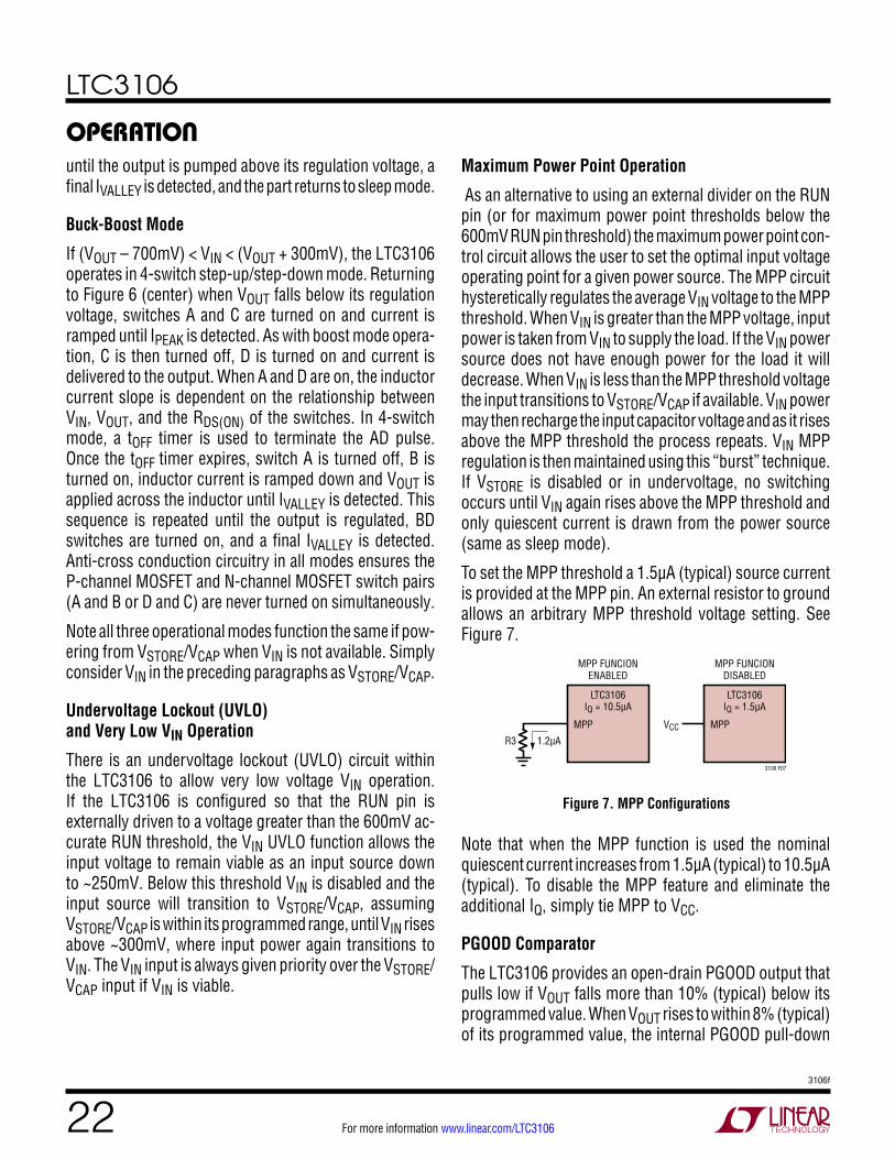
Maximum Power Point Operation
As an alternative to using an external divider on the RUN pin (or for maximum power point thresholds below the 600mV RUN pin threshold) the maximum power point con-trol circuit allows the user to set the optimal input voltage operating point for a given power source. The MPP circuit hysteretically regulates the average VIN voltage to the MPP threshold. When VIN is greater than the MPP voltage, input power is taken from VIN to supply the load. If the VIN power source does not have enough power for the load it will decrease. When VIN is less than the MPP threshold voltage the input transitions to VSTORE/VCAP if available. VIN power may then recharge the input capacitor voltage and as it rises above the MPP threshold the process repeats. VIN MPP regulation is then maintained using this “burst” technique. If VSTORE is disabled or in undervoltage, no switching occurs until VIN again rises above the MPP threshold and only quiescent current is drawn from the power source (same as sleep mode).
To set the MPP threshold a 1.5µA (typical) source current is provided at the MPP pin. An external resistor to ground allows an arbitrary MPP threshold voltage setting. See Figure 7.
MPP
1.2µAR3
3106 F07
LTC3106IQ = 10.5µA
MPP FUNCIONENABLED
MPPVCC
LTC3106IQ = 1.5µA
MPP FUNCIONDISABLED
Note that when the MPP function is used the nominal quiescent current increases from 1.5µA (typical) to 10.5µA (typical). To disable the MPP feature and eliminate the additional IQ, simply tie MPP to VCC.
PGOOD Comparator
The LTC3106 provides an open-drain PGOOD output that pulls low if VOUT falls more than 10% (typical) below its programmed value. When VOUT rises to within 8% (typical) of its programmed value, the internal PGOOD pull-down
LTC3106
233106f
For more information www.linear.com/LTC3106
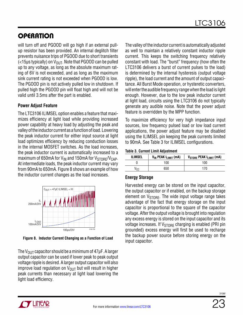
Figure 8. Inductor Current Changing as a Function of Load
operaTionwill turn off and PGOOD will go high if an external pull-up resistor has been provided. An internal deglitch filter prevents nuisance trips of PGOOD due to short transients (<15µs typically) on VOUT. Note that PGOOD can be pulled up to any voltage, as long as the absolute maximum rat-ing of 6V is not exceeded, and as long as the maximum sink current rating is not exceeded when PGOOD is low. The PGOOD pin is not actively pulled low in shutdown. If pulled high the PGOOD pin will float high and will not be valid until 3.5ms after the part is enabled.
Power Adjust Feature
The LTC3106 ILIMSEL option enables a feature that maxi-mizes efficiency at light load while providing increased power capability at heavy load by adjusting the peak and valley of the inductor current as a function of load. Lowering the peak inductor current for either input source at light load optimizes efficiency by reducing conduction losses in the internal MOSFET switches. As the load increases, the peak inductor current is automatically increased to a maximum of 650mA for VIN and 150mA for VSTORE/VCAP. At intermediate loads, the peak inductor current may vary from 90mA to 650mA. Figure 8 shows an example of how the inductor current changes as the load increases.
The valley of the inductor current is automatically adjusted as well to maintain a relatively constant inductor ripple current. This keeps the switching frequency relatively constant with load. The “burst” frequency (how often the LTC3106 delivers a burst of current pulses to the load) is determined by the internal hysteresis (output voltage ripple), the load current and the amount of output capaci-tance. All Burst Mode operation, or hysteretic converters, will enter the audible frequency range when the load is light enough. However, due to the low peak inductor current at light load, circuits using the LTC3106 do not typically generate any audible noise. Note that the power adjust feature is overridden by the MPP function.
To maximize efficiency for very high impedance input sources, low frequency pulsed load or low load current applications, the power adjust feature may be disabled using the ILIMSEL pin keeping the peak currents limited to 90mA. See Table 3 for ILIMSEL configurations.
Table 3. Current Limit AdjustmentILIMSEL VIN PEAK ILIMIT (mA) VSTORE PEAK ILIMIT (mA)
0 100 100
VCC 650 170
Energy Storage
Harvested energy can be stored on the input capacitor, the output capacitor or if enabled, on the backup storage element on VSTORE. The wide input voltage range takes advantage of the fact that energy storage on the input capacitor is proportional to the square of the capacitor voltage. After the output voltage is brought into regulation any excess energy is stored on the input capacitor and its voltage increases. If VSTORE charging is enabled (PRI pin grounded) excess energy will first be used to recharge the backup power source before storing energy on the input capacitor.
COUT = 47µF, ILIMSEL = HI
100µs/DIV
IL200mA/DIV
ILOAD100mA/DIV
3106 F08
The VOUT capacitor should be a minimum of 47μF. A larger output capacitor can be used if lower peak to peak output voltage ripple is desired. A larger output capacitor will also improve load regulation on VOUT but will result in higher peak currents than necessary at light load lowering the light load efficiency.
LTC3106
243106f
For more information www.linear.com/LTC3106
applicaTions inForMaTionA standard application circuit for the LTC3106 is shown on the front page of this data sheet, although the LTC3106 can be configured to work from a variety of alternative energy and backup battery sources. The appropriate selection of external components is dependent upon the required performance of the IC in each particular application. This section of the data sheet provides some basic guidelines and considerations to aid in the selection of external com-ponents and the design of the applications circuit, as well as a few other application circuit examples.
VSTORE/VCAP Capacitor Selection
If there is insufficient power on VIN, the VSTORE/VCAP input carries the full inductor current and provides power to internal control circuits in the IC. To minimize VSTORE voltage ripple and ensure proper operation of the IC, a low ESR bypass capacitor with a value of at least 4.7μF should be located as close to the VCAP pin as possible. The traces connecting this capacitor to VCAP and the ground plane should be made as short as possible. In cases where the series resistance of the battery is high or the LTC3106 is powered by long traces or leads, a larger value bulk input capacitor may be required and is generally recommended. In such applications a 47μF to 100μF low ESR electrolytic capacitor in parallel with a 1μF ceramic capacitor generally yields a high performance, low cost solution. Note that if there is sufficient power on VIN only capacitor leakage current and shutdown current will be drawn from the VSTORE/VCAP source. When using the Shelf Mode feature, the VSTORE pin should be isolated from the VCAP pin and no capacitor is needed on the VSTORE pin. Instead the bypass capacitor should be located only on the VCAP pin.
VIN and VOUT Capacitor Selection
The LTC3106 has no maximum capacitance limitation on VIN or VOUT but there is a slew rate limitation on VIN that drives the need for a minimum input capacitance. Refer to the plot of Maximum Slew Rate vs Input Voltage in the Typical Performance Characteristics section. For general applications where the input source has a low impedance and relatively high output power, a minimum 22μF ceramic capacitor is recommended between VIN and GND. In ap-plications where the input has a high impedance and may
be intermittent, such as in energy harvesting applications, the total VIN capacitor value will be selected to optimize the use of the harvested source and will typically be greater than 100μF.
In energy harvesting applications the VIN and VOUT capaci-tors should be selected to optimize the use of the harvested source. Input capacitor selection is highly important if the LTC3106 must start from a, high source resistance system on VIN. When using bulk input capacitors that have high ESR, a small valued parallel ceramic capacitor should be placed between VIN and GND as close to the converter pins as possible. After VAUX and the output voltage are brought into regulation any excess energy is stored on the input capacitor and its voltage will increase. Care should be taken to ensure the open-circuit voltage of the harvested source does not exceed or is appropriately clamped to the maximum operating voltage VIN and that the input capacitor is rated for that voltage.
For pulsed load applications, even low power pulsed load applications such as Eterna® BLE, ZigBee as well as other proprietary low power RF protocols, the input capacitor should be sized to store enough energy to provide out-put power for the duration of the load profile. If enough energy is stored so that VIN does not reach the chosen falling threshold during a load transient then the VSTORE/VCAP current will be minimized thereby maximizing battery life. Spacing load transients so that the average power required to service the application is less than or equal to the power available from the energy harvesting source will also greatly extend the life of the battery. The following equation can be used to size the input capacitor to meet the power requirements of the output for the desired duration:
CVIN =2/η• VOUT • ΣInTn( )VINOV
2 – VINUV2( ) µF( )
Here η is the average efficiency of the converter over the input voltage range and VIN is the input voltage when the converter begins to switch. Typically VIN(OV) will be the selected input voltage rising threshold. VIN(UV) is the VIN(OV) minus the hysteresis voltage. ∑InTn is the area under each of the load pulses for given load profile. This equation may overestimate the input capacitor necessary. It may be
LTC3106
253106f
For more information www.linear.com/LTC3106
applicaTions inForMaTionacceptable to allow the load current to deplete the output capacitor all the way to the lower PGOOD threshold. The equation also assumes that the input source charging has a negligible effect during this time. Example uses of this equation to size input capacitors are included in the design examples later in this section.
The duration for which the regulator sleeps depends on the load current and the size of the VOUT capacitor. The sleep time decreases as the load current increases and/or as the output capacitor decreases. The VOUT capaci-tor should be a minimum of 47μF. A larger output capacitor can be used if lower peak-to-peak output voltage ripple is desired. A larger output capacitor will also improve load regulation on VOUT. Multilayer ceramic or low ESR electrolytic capacitors are both excellent options.
Proper sizing of the input capacitor to optimize energy storage at the input utilizes the potential for higher input voltages and higher efficiency. Ultimately the output current is limited by what the converter can supply from its input. If a larger peak transient load needs to be serviced, the output capacitor should be sized to support the larger cur-rent for the duration of the load transient by the following:
COUT ≥ILOAD •
tPULSEVDROOP
COUT is the output capacitor value (µF) required, ILOAD is the peak transient load current (mA), tPULSE is the duration of that transient (ms) and VDROOP is the amount of voltage droop the circuit can tolerate (both in V).
For many of the LTC3106 applications, the input capaci-tor values can be quite large (>1mF). A list of high value storage capacitor manufacture’s is listed in Table 4. For larger bulk output capacitors an additional low effective series resistance (ESR) output capacitor of 10μF should be added and connected as close to the IC pin as possible.
Regardless of its value, the selected output capacitor must be rated higher than the voltage selected for VOUT by OS1 and OS2. Likewise the selected input capacitor must be rated higher than the open-circuit voltage of the VIN source.
Table 4. Recommended Bulk Storage Capacitor VendorsVENDOR PART
AVX BestCap Series TAJ, TPS Series Tantalum
Vishay 595D Series (Tantalum) 153 CRV (Aluminum, Low Leakage) 150 CRZ (Aluminum, Low Leakage) 196 DLC (Double Layer Aluminum)
Illinois Capacitor RKR Series (Aluminum, Low Leakage) DCN Series
Cooper Bussman KR Series KW Series PA, PB, PM, PH Series
Cap-XX G Series (Dual Cell) H Series (Dual Cell)
VCC Capacitor Selection
The VCC output of the LTC3106 is generated from the great-est of VIN, VCAP, VAUX or VOUT. A low ESR 0.1μF capacitor should be used. The capacitor should be located close to the VCC pin and through the shortest ground traces possible.
VAUX Capacitor Selection
A minimum 2.2µF low ESR capacitor must be used to decouple VAUX although 4.7μF is more typical for many applications. Smaller capacitor sizes help reduce VOUT ripple especially at high load currents while larger capacitor sizes improve start-up at low output voltages. The capaci-tor should be located as close to the VAUX pin as possible.
As mentioned in the operations section the AUX D switch and the VOUT D switch are in parallel. Asynchronous diode conduction will occur when either VAUX or VOUT is being serviced by the buck/boost circuitry. For this reason it is recommended to keep a 10:1 ratio of VOUT to VAUX capacitor to ensure a proper start-up with low voltage, high impedance sources. Under most load conditions the output voltage will be maintained normally although under true zero load conditions (<500nA) the parasitic current from VAUX to VOUT could force VOUT to regulate up to 5% higher than typical.
LTC3106
263106f
For more information www.linear.com/LTC3106
applicaTions inForMaTionUse of Ceramic Capacitors
To minimize losses in low power systems all capacitors should have low leakage current. Ceramic capacitors are recommended for use in LTC3106 applications due to their small size, low ESR and low leakage currents. However, many ceramic capacitors intended for power applications experience a significant loss in capacitance from their rated value as the DC bias voltage on the capacitor increases. It is not uncommon for a small surface mount capacitor to lose more than 50% of its rated capacitance when operated at even half of its maximum rated voltage. This effect is generally reduced as the case size is increased for the same nominal value capacitor. As a result, it is often necessary to use a larger value capacitance or a higher voltage rated capacitor than would ordinarily be required to actually realize the intended capacitance at the operating voltage of the application. X5R and X7R dielectric types are recommended as they exhibit the best performance over the wide operating range and temperature of the LTC3106. To verify that the intended capacitance is achieved in the application circuit, be sure to consult the capacitor vendor’s curve of capacitance versus DC bias voltage.
PGOOD Output
The PGOOD output can also help with power manage-ment. PGOOD transitions high the first time the output reaches regulation and stays high until the output falls to 92% of the regulation point. PGOOD can be used to trigger a system load. For example, a current burst could begin when PGOOD goes high and would continuously deplete the output capacitor until PGOOD went low. Note the PGOOD pin will remain high if the output is still within 92% of the regulation point, even if the input falls below the lower UVLO threshold.
Inductor Selection
Low DCR power inductors with values between 4.7μH and 10μH are suitable for use with the LTC3106. Inductor vendor information can be found in Table 5. For most applications, a 10μH inductor is recommended. In applications where the input voltage is very low, a larger value inductor can provide higher efficiency and a lower start-up voltage.
In applications where the input voltage is relatively high (VIN > 0.8V), smaller inductors may be used to provide a smaller overall footprint. In all cases, the inductor must have a low DCR and a saturation current rating greater than the highest typical peak current limit setting as listed in the Electrical Characteristics table. If the DC resistance of the inductor is too high, efficiency will be reduced and the minimum operating voltage will increase. Note the inductor value will have a direct effect on the switching frequency.
Table 5. Inductor Vendor InformationVENDOR PART
Coilcraft www.coilcraft.com
EPL2014, EPL3012, EPL3015, LPS3015, LPS3314, XFL3012
Coiltronics www.cooperindustries.com
SDH3812, SD3814, SD3114, SD3118
Murata www.murata.com
LQH3NP, LQH32P, LQH44P
Sumida www.sumida.com
CDRH2D16, CDRH2D18, CDRH3D14, CDRH3D16
Taiyo-Yuden www.t-yuden.com
NR3012T, NR3015T, NRS4012T, BRC2518
TDK www.tdk.com
VLS3012, VLS3015, VLF302510MT, VLF302512MT
Toko www.tokoam.com
DP3015C, DB3018C, DB3020C, DP418C, DP420C, DEM2815C, DFE322512C, DFE252012C
Würth www.we-online.com
WE-TPC 2813, WE-TPC 3816, WE-TPC 2828
Maximum Power Point Threshold Configuration
There are two methods for maintaining the maximum power point of an input source on VIN. Already discussed in this data sheet is a resistive divider on the RUN pin monitoring VIN. This is useful for >600mV MPP set points. The LTC3106 also has a dedicated MPP function that can be used over the full input voltage range as well as input voltages between the UVLO and RUN pin thresholds. Note that the LTC3106 IQ increases from 1.6µA (typ) to 10.6µA (typ) if the MPPC pin functionality is enabled.
The MPP circuit hysteretically controls VIN by setting a lower voltage threshold on the MPP pin. If VIN drops below the MPP threshold the converter will stop draw-ing power from VIN and force a sleep signal. If VSTORE is within the proper operating range, the output power will then be taken from VSTORE. If however there is not a valid
LTC3106
273106f
For more information www.linear.com/LTC3106
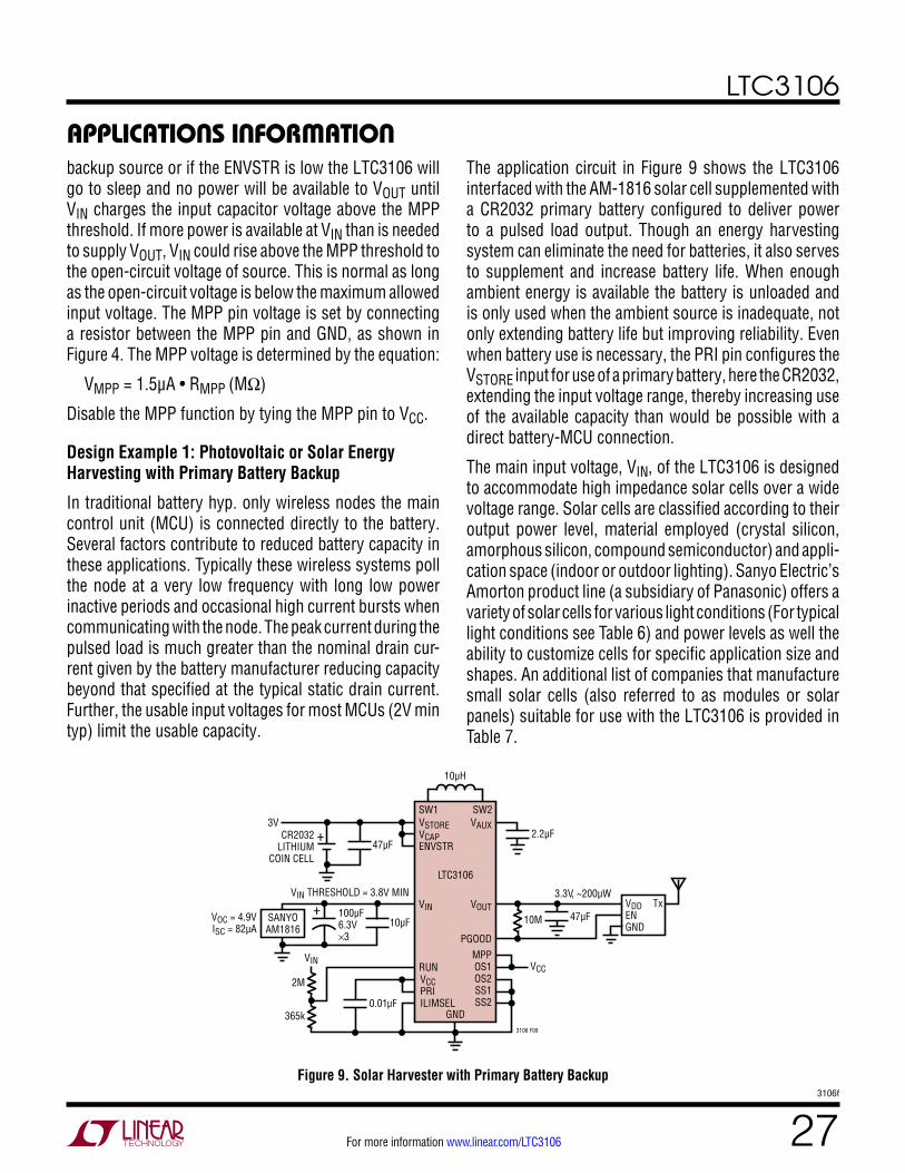
applicaTions inForMaTionbackup source or if the ENVSTR is low the LTC3106 will go to sleep and no power will be available to VOUT until VIN charges the input capacitor voltage above the MPP threshold. If more power is available at VIN than is needed to supply VOUT, VIN could rise above the MPP threshold to the open-circuit voltage of source. This is normal as long as the open-circuit voltage is below the maximum allowed input voltage. The MPP pin voltage is set by connecting a resistor between the MPP pin and GND, as shown in Figure 4. The MPP voltage is determined by the equation:
VMPP = 1.5μA • RMPP (MΩ)
Disable the MPP function by tying the MPP pin to VCC.
Design Example 1: Photovoltaic or Solar Energy Harvesting with Primary Battery Backup
In traditional battery hyp. only wireless nodes the main control unit (MCU) is connected directly to the battery. Several factors contribute to reduced battery capacity in these applications. Typically these wireless systems poll the node at a very low frequency with long low power inactive periods and occasional high current bursts when communicating with the node. The peak current during the pulsed load is much greater than the nominal drain cur-rent given by the battery manufacturer reducing capacity beyond that specified at the typical static drain current. Further, the usable input voltages for most MCUs (2V min typ) limit the usable capacity.
The application circuit in Figure 9 shows the LTC3106 interfaced with the AM-1816 solar cell supplemented with a CR2032 primary battery configured to deliver power to a pulsed load output. Though an energy harvesting system can eliminate the need for batteries, it also serves to supplement and increase battery life. When enough ambient energy is available the battery is unloaded and is only used when the ambient source is inadequate, not only extending battery life but improving reliability. Even when battery use is necessary, the PRI pin configures the VSTORE input for use of a primary battery, here the CR2032, extending the input voltage range, thereby increasing use of the available capacity than would be possible with a direct battery-MCU connection.
The main input voltage, VIN, of the LTC3106 is designed to accommodate high impedance solar cells over a wide voltage range. Solar cells are classified according to their output power level, material employed (crystal silicon, amorphous silicon, compound semiconductor) and appli-cation space (indoor or outdoor lighting). Sanyo Electric’s Amorton product line (a subsidiary of Panasonic) offers a variety of solar cells for various light conditions (For typical light conditions see Table 6) and power levels as well the ability to customize cells for specific application size and shapes. An additional list of companies that manufacture small solar cells (also referred to as modules or solar panels) suitable for use with the LTC3106 is provided in Table 7.
Figure 9. Solar Harvester with Primary Battery Backup
+
10µH
VSTOREVCAPENVSTR
VCCPRIILIMSEL
VAUXCR2032
LITHIUMCOIN CELL
3V
VOUT
MPPOS1OS2SS1SS2
GND
SW1 SW2
LTC3106
VIN
RUN
10M
365k
2M
VOC = 4.9VISC = 82µA
VIN VCC
3106 F09
2.2µF
47µF
3.3V, ~200µWVIN THRESHOLD = 3.8V MIN
47µF
10µF
0.01µF
100µF6.3V×3
+SANYOAM1816
VDDENGND
Tx
PGOOD
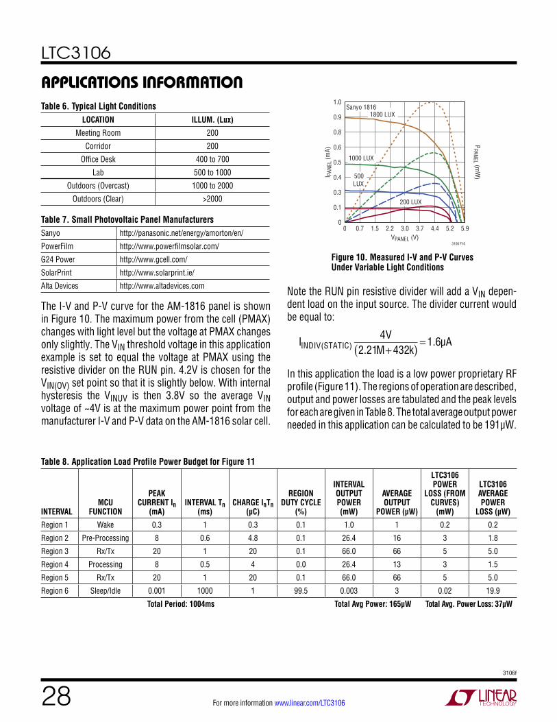
LTC3106
283106f
For more information www.linear.com/LTC3106
applicaTions inForMaTionTable 6. Typical Light Conditions
LOCATION ILLUM. (Lux)
Meeting Room 200
Corridor 200
Office Desk 400 to 700
Lab 500 to 1000
Outdoors (Overcast) 1000 to 2000
Outdoors (Clear) >2000
Table 7. Small Photovoltaic Panel ManufacturersSanyo http://panasonic.net/energy/amorton/en/
PowerFilm http://www.powerfilmsolar.com/
G24 Power http://www.gcell.com/
SolarPrint http://www.solarprint.ie/
Alta Devices http://www.altadevices.com
The I-V and P-V curve for the AM-1816 panel is shown in Figure 10. The maximum power from the cell (PMAX) changes with light level but the voltage at PMAX changes only slightly. The VIN threshold voltage in this application example is set to equal the voltage at PMAX using the resistive divider on the RUN pin. 4.2V is chosen for the VIN(OV) set point so that it is slightly below. With internal hysteresis the VINUV is then 3.8V so the average VIN voltage of ~4V is at the maximum power point from the manufacturer I-V and P-V data on the AM-1816 solar cell.
Note the RUN pin resistive divider will add a VIN depen-dent load on the input source. The divider current would be equal to:
IINDIV(STATIC)
4V2.21M+ 432k( ) = 1.6µA
In this application the load is a low power proprietary RF profile (Figure 11). The regions of operation are described, output and power losses are tabulated and the peak levels for each are given in Table 8. The total average output power needed in this application can be calculated to be 191µW.
Figure 10. Measured I-V and P-V Curves Under Variable Light Conditions
Table 8. Application Load Profile Power Budget for Figure 11
INTERVALMCU
FUNCTION
PEAK CURRENT In
(mA)INTERVAL Tn
(ms)CHARGE InTn
(µC)
REGION DUTY CYCLE
(%)
INTERVAL OUTPUT POWER (mW)
AVERAGE OUTPUT
POWER (µW)
LTC3106 POWER
LOSS (FROM CURVES)
(mW)
LTC3106 AVERAGE POWER
LOSS (µW)
Region 1 Wake 0.3 1 0.3 0.1 1.0 1 0.2 0.2
Region 2 Pre-Processing 8 0.6 4.8 0.1 26.4 16 3 1.8
Region 3 Rx/Tx 20 1 20 0.1 66.0 66 5 5.0
Region 4 Processing 8 0.5 4 0.0 26.4 13 3 1.5
Region 5 Rx/Tx 20 1 20 0.1 66.0 66 5 5.0
Region 6 Sleep/Idle 0.001 1000 1 99.5 0.003 3 0.02 19.9
Total Period: 1004ms Total Avg Power: 165µW Total Avg. Power Loss: 37µW
1800 LUX
1000 LUX
500LUX
200 LUX
Sanyo 1816
VPANEL (V)0 0.7 1.5 2.2 3.0 3.7 4.4 5.2 5.9
0
0.1
0.3
0.4
0.5
0.6
0.8
0.9
1.0
I PAN
EL (m
A)
PPANEL (m
W)
3106 F10
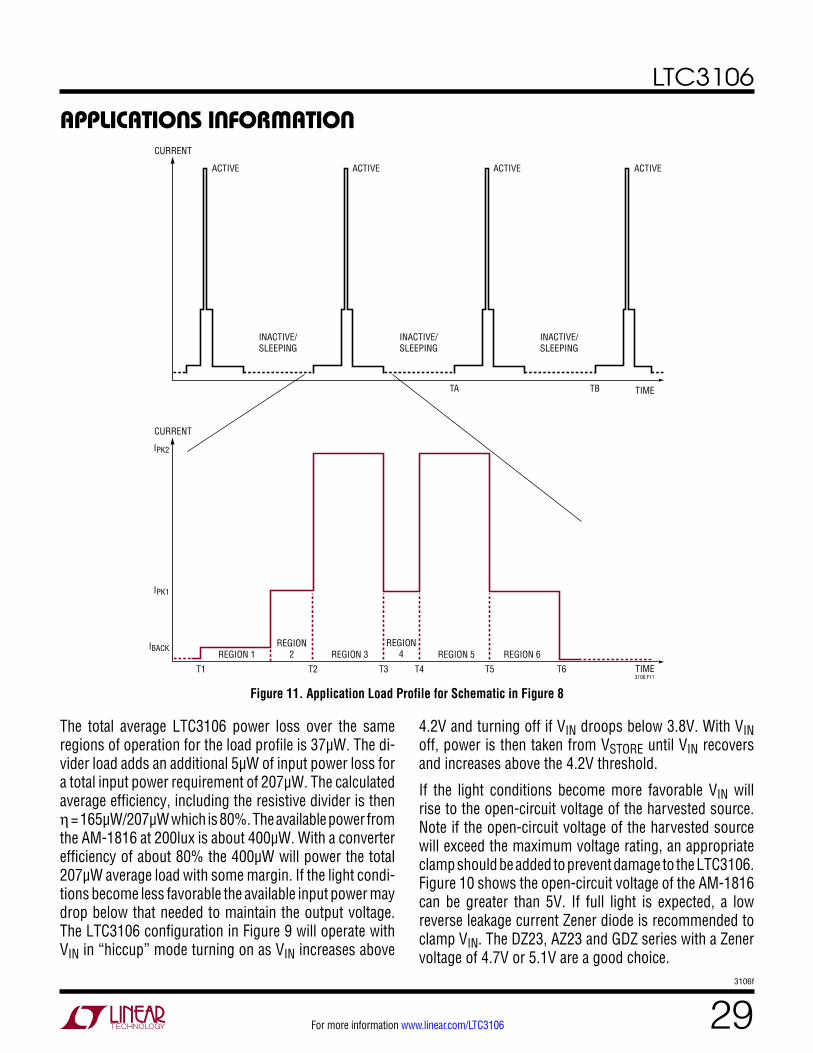
LTC3106
293106f
For more information www.linear.com/LTC3106
applicaTions inForMaTion
Figure 11. Application Load Profile for Schematic in Figure 8
The total average LTC3106 power loss over the same regions of operation for the load profile is 37µW. The di-vider load adds an additional 5µW of input power loss for a total input power requirement of 207µW. The calculated average efficiency, including the resistive divider is then η = 165µW/207µW which is 80%. The available power from the AM-1816 at 200lux is about 400µW. With a converter efficiency of about 80% the 400µW will power the total 207µW average load with some margin. If the light condi-tions become less favorable the available input power may drop below that needed to maintain the output voltage. The LTC3106 configuration in Figure 9 will operate with VIN in “hiccup” mode turning on as VIN increases above
4.2V and turning off if VIN droops below 3.8V. With VIN off, power is then taken from VSTORE until VIN recovers and increases above the 4.2V threshold.
If the light conditions become more favorable VIN will rise to the open-circuit voltage of the harvested source. Note if the open-circuit voltage of the harvested source will exceed the maximum voltage rating, an appropriate clamp should be added to prevent damage to the LTC3106. Figure 10 shows the open-circuit voltage of the AM-1816 can be greater than 5V. If full light is expected, a low reverse leakage current Zener diode is recommended to clamp VIN. The DZ23, AZ23 and GDZ series with a Zener voltage of 4.7V or 5.1V are a good choice.
TIME
TIME3106 F11
T6T5T4T3T2T1
IBACK
IPK1
IPK2
REGION 6REGION 5REGION
4REGION 3REGION
2REGION 1
CURRENT
CURRENT
ACTIVE ACTIVE ACTIVE ACTIVE
TBTA
INACTIVE/SLEEPING
INACTIVE/SLEEPING
INACTIVE/SLEEPING
LTC3106
303106f
For more information www.linear.com/LTC3106
applicaTions inForMaTionTo optimize use of the harvested source and increase the battery life of the backup source it is important to size the input capacitor to handle the average power load for the load profile at the lowest light level. Referring again to Table 8 to sum the required charge for the load and using the input capacitor sizing equation:
CVIN =2/η• VOUT • ΣlnTn( )VIN(OV)
2 – VIN(UV)2( ) µF( )
The average efficiency (η) with VIN = 4.2V and VOUT = 3.3V is 0.8. The VIN(OV) and VIN(UV) thresholds are already determined and ∑InTn can be found in the load profile table. CVIN is found to be 184µF. A single 220µF low leakage Tantalum chip capacitor could be used. For the lowest leakage solution and to add design margin 2× 100µF, 6.3V, ±10% ceramic capacitors are selected.
If the VIN source is unavailable the primary battery on VSTORE will continue to supply the load. To offload the peak current load from the battery and minimize the effect of high peak currents degrading the rated battery capacity the lowest peak current setting on the LTC3106 is chosen. In addition, the VSTORE capacitor design should follow that of the VIN capacitor. Using the same method but replacing the OV and UV thresholds with the max and min VSTORE input voltages the value of the VSTORE capacitor is calculated to be 38µF. For design margin a low ESR 10V, 47µF ceramic capacitor is used.
Design Example 2: Thermoelectric Harvesting from Peltier cell (TEG) with Rechargeable Battery Backup
A Peltier cell (also known as a thermoelectric cooler) is made up of a large number of series-connected P-N junctions, sandwiched between two parallel ceramic plates. Although Peltier cells are often used as coolers by applying a DC voltage to their inputs, they will also generate a DC output voltage, using the Seebeck effect, when the two plates are at different temperatures. The polarity of the output voltage will depend on the polarity of the temperature differential between the plates. The magnitude of the output voltage is proportional to the magnitude of the temperature dif-ferential between the plates. In this manner, a Peltier cell is referred to as a thermoelectric generator (TEG).
Peltier cells are available in a wide range of sizes and power capabilities, from less than 10mm square to over 50mm square. They are typically 2mm to 5mm in height. A list of Peltier cell manufacturers is given in Table 9.
Table 9. Peltier Cell ManufacturersMicropelt www.micropelt.com
CUI, Inc www.cui.com (Distributor)
Fujitaka www.fujitaka.com/pub/peltier/english/thermoelectric_power.html
Ferrotec www.ferrotec.com/products/thermal/modules
Kryotherm www.kryothermusa.com
Laird Technologies www.lairdtech.com
Marlow Industries www.marlow.com
Nextreme www.nextreme.com
TE Technology www.tetech.com/Peltier-Thermoelectirc-Cooler-Modules.html
Tellurex www.tellurex.com
The low voltage capability of the LTC3106 design allows it to operate from a TEG with temperature differentials as low as 20°C, making it ideal for harvesting energy in many industrial applications in which a temperature difference exists between two surfaces or between a surface and the ambient environment.
The application circuit in Figure 12 shows the LTC3106 interfaced with a TEG supplemented with a Li-ion recharge-able (secondary) battery, both configured to deliver power to a low power pulsed load output. With the RUN pin con-nected to VSTORE, the application circuit is configured to take advantage of the 300mV input voltage UVLO. In this configuration VIN will operate in “hiccup” mode turning on as VIN increases above 0.3V and turning off if VIN droops 50mV below 0.3V to maintain an average power to the output without allowing the input to fall to zero. Assuming a good battery voltage the output power will be supplied by the battery when the input voltage drops below the UVLO threshold and transition back to the input when the input charges up above the UVLO threshold.
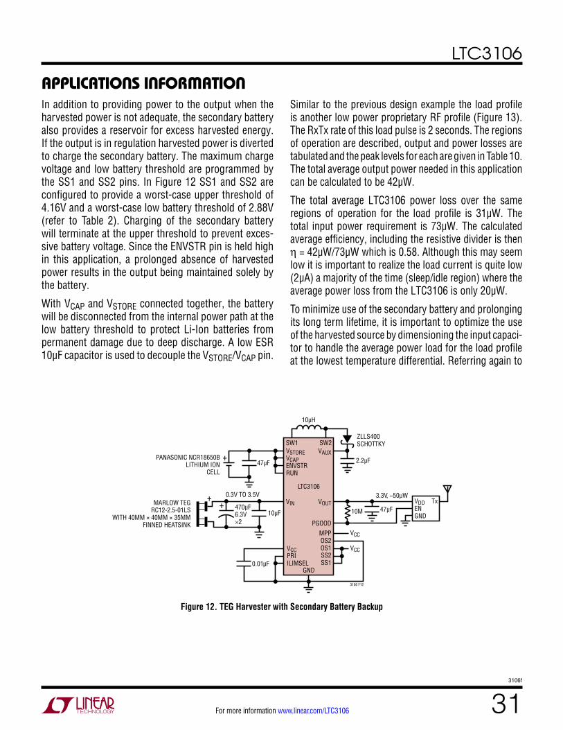
LTC3106
313106f
For more information www.linear.com/LTC3106
applicaTions inForMaTionIn addition to providing power to the output when the harvested power is not adequate, the secondary battery also provides a reservoir for excess harvested energy. If the output is in regulation harvested power is diverted to charge the secondary battery. The maximum charge voltage and low battery threshold are programmed by the SS1 and SS2 pins. In Figure 12 SS1 and SS2 are configured to provide a worst-case upper threshold of 4.16V and a worst-case low battery threshold of 2.88V (refer to Table 2). Charging of the secondary battery will terminate at the upper threshold to prevent exces-sive battery voltage. Since the ENVSTR pin is held high in this application, a prolonged absence of harvested power results in the output being maintained solely by the battery.
With VCAP and VSTORE connected together, the battery will be disconnected from the internal power path at the low battery threshold to protect Li-Ion batteries from permanent damage due to deep discharge. A low ESR 10µF capacitor is used to decouple the VSTORE/VCAP pin.
Figure 12. TEG Harvester with Secondary Battery Backup
Similar to the previous design example the load profile is another low power proprietary RF profile (Figure 13). The RxTx rate of this load pulse is 2 seconds. The regions of operation are described, output and power losses are tabulated and the peak levels for each are given in Table 10. The total average output power needed in this application can be calculated to be 42µW.
The total average LTC3106 power loss over the same regions of operation for the load profile is 31µW. The total input power requirement is 73µW. The calculated average efficiency, including the resistive divider is then η = 42µW/73µW which is 0.58. Although this may seem low it is important to realize the load current is quite low (2µA) a majority of the time (sleep/idle region) where the average power loss from the LTC3106 is only 20µW.
To minimize use of the secondary battery and prolonging its long term lifetime, it is important to optimize the use of the harvested source by dimensioning the input capaci-tor to handle the average power load for the load profile at the lowest temperature differential. Referring again to
+
10µH
VSTOREVCAPENVSTRRUN
VCCPRIILIMSEL
VAUXPANASONIC NCR18650B
LITHIUM IONCELL
VOUT
MPPOS2OS1SS2SS1
GND
SW1 SW2
LTC3106
VIN10M
VCC
VCC
3106 F12
2.2µF
ZLLS400SCHOTTKY
47µF
3.3V, ~50µW0.3V TO 3.5V
47µF
10µF
MARLOW TEGRC12-2.5-01LS
WITH 40MM × 40MM × 35MMFINNED HEATSINK
+
0.01µF
470µF6.3V×2
+ VDDENGND
Tx
PGOOD
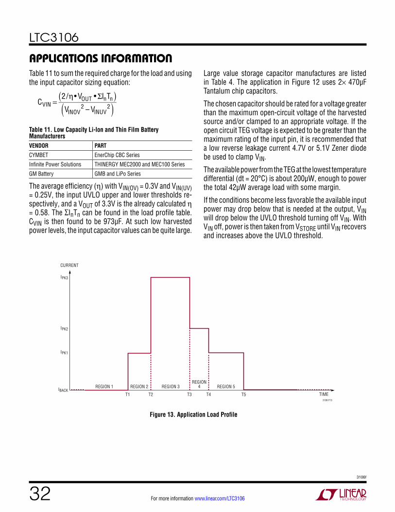
LTC3106
323106f
For more information www.linear.com/LTC3106
applicaTions inForMaTionTable 11 to sum the required charge for the load and using the input capacitor sizing equation:
CVIN =2/η• VOUT • ΣlnTn( )VINOV
2 – VINUV2( )
Table 11. Low Capacity Li-Ion and Thin Film Battery ManufacturersVENDOR PART
CYMBET EnerChip CBC Series
Infinite Power Solutions THINERGY MEC2000 and MEC100 Series
GM Battery GMB and LiPo Series
The average efficiency (η) with VIN(OV) = 0.3V and VIN(UV) = 0.25V, the input UVLO upper and lower thresholds re-spectively, and a VOUT of 3.3V is the already calculated η = 0.58. The ∑InTn can be found in the load profile table. CVIN is then found to be 973µF. At such low harvested power levels, the input capacitor values can be quite large.
Large value storage capacitor manufactures are listed in Table 4. The application in Figure 12 uses 2× 470µF Tantalum chip capacitors.
The chosen capacitor should be rated for a voltage greater than the maximum open-circuit voltage of the harvested source and/or clamped to an appropriate voltage. If the open circuit TEG voltage is expected to be greater than the maximum rating of the input pin, it is recommended that a low reverse leakage current 4.7V or 5.1V Zener diode be used to clamp VIN.
The available power from the TEG at the lowest temperature differential (dt = 20°C) is about 200µW, enough to power the total 42µW average load with some margin.
If the conditions become less favorable the available input power may drop below that is needed at the output, VIN will drop below the UVLO threshold turning off VIN. With VIN off, power is then taken from VSTORE until VIN recovers and increases above the UVLO threshold.
Figure 13. Application Load Profile
TIME3106 F13
T5T4T3T2T1IBACK
IPK1
IPK3
IPK2
REGION 5REGION
4REGION 3REGION 2REGION 1
CURRENT
LTC3106
333106f
For more information www.linear.com/LTC3106
Table 10. Application Load Profile Power Budget for Figure 11
INTERVAL MCU FUNCTION
PEAK CURRENT In
(mA)INTERVAL Tn
(ms)CHARGE InTn
(µC)
REGION DUTY CYCLE
(%)
INTERVAL OUTPUT POWER (mW)
AVERAGE OUTPUT
POWER (µW)
LTC3106 POWER
LOSS (FROM CURVES)
(mW)
LTC3106 AVERAGE
POWER LOSS (µW)
Region 1 Sleep/Idle 0.002 2000 4 99.85 0.007 7 0.2 20.0
Region 2 Pre-Processing 1.7 0.6 1.02 0.03 56 2 3 0.9
Region 3 Tx 17 1 17 0.05 53.1 28 5 7.5
Region 4 Rx 4 0.5 2 0.02 13.2 3 3 1.2
Region 5 Post-Processing 1.7 1 1.7 0.05 5.6 3 5 1.5
Total Period: 2003ms Total Avg Power: 42.37µW Total Avg. Power Loss: 31µW
applicaTions inForMaTionIf conditions become more favorable the input capacitor will charge to a higher voltage terminating at the open-circuit voltage of the harvested source. When the output is idle under these conditions, excess energy is used to maintain the charge on the VSTORE battery. Any remaining excess energy will be stored on the input capacitor and VIN will rise to the open-circuit voltage of the harvested source. As already mentioned, if the open-circuit voltage of the harvested source will exceed the maximum voltage
rating of the pin an appropriate clamp should be added to prevent damage to the LTC3106.
Most MCUs, even low power wireless specific MCUs, still load the LTC3106 output with a small current. If, however, the load current will be less than 400nA the output regulation error can increase to 5% of the nominal output voltage depending on sleep period and the size of the output capacitor.
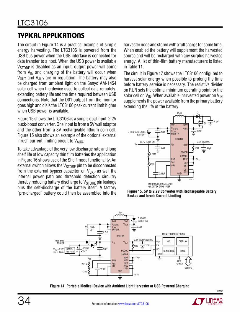
LTC3106
343106f
For more information www.linear.com/LTC3106
The circuit in Figure 14 is a practical example of simple energy harvesting. The LTC3106 is powered from the USB bus power when the USB interface is connected for data transfer to a host. When the USB power is available VSTORE is disabled as an input, output power will come from VIN and charging of the battery will occur when VOUT and VAUX are in regulation. The battery may also be charged from ambient light on the Sanyo AM-1454 solar cell when the device used to collect data remotely, extending battery life and the time required between USB connections. Note that the D01 output from the monitor goes high and dials the LTC3106 peak current limit higher when USB power is available.
Figure 15 shows the LTC3106 as a simple dual input, 2.2V buck-boost converter. One input is from a 5V wall adaptor and the other from a 3V rechargeable lithium coin cell. Figure 15 also shows an example of the optional external inrush current limiting circuit to VAUX.
To take advantage of the very low discharge rate and long shelf life of low capacity thin film batteries the application in Figure 16 shows use of the Shelf mode functionality. An external switch allows the VSTORE pin to be disconnected from the external bypass capacitor on VCAP as well the internal power path and threshold detection circuitry thereby reducing battery discharge to VSTORE pin leakage plus the self-discharge of the battery itself. A factory “pre-charged” battery could then be assembled into the
harvester node and stored with a full charge for some time. When enabled the battery will supplement the harvested source and will be recharged with any surplus harvested energy. A list of thin-film battery manufacturers is listed in Table 11.The circuit in Figure 17 shows the LTC3106 configured to harvest solar energy when possible to prolong the time before battery service is necessary. The resistive divider on RUN sets the optimal minimum operating point for the solar cell on VIN. When available, harvested power on VIN supplements the power available from the primary battery extending the life of the battery.
Typical applicaTions
Figure 14. Portable Medical Device with Ambient Light Harvester or USB Powered Charging
10µH
PRI
VAUX
VOUT
ILIMSELMPP
OS2SS1
OS1SS2GND
SW1 SW2
LTC3106
VIN5V
RUN
10M
432k
D1: DIODES INC ZLLS400Q1: ZETEX ZMX61P03F
2.21M
VCC
3106 F15
2.2µF
0.1µF
47µF
2.2V (300mA)(3.7V TURN ON)
47µF
22µF
0.01µF
PGOOD
VCC
+VSTOREVCAPENVSTR
Li RECHARGEABLEBATTERY
Q1
D1
10µH
VSTOREVCAPENVSTR
VCCPRI
VAUX
VOUT
MPPOS1SS2OS2SS1
GND
SW1 SW2
LTC3106
VIN
RUN
10M
1.33M
2.21M
VOC = 2.4VISC = 35µA
VIN VCC
3106 F14
2.2µFNiMH×2
47µF
GNDSENSOR(S)
USB I/O
USBPOWER
VDDEN
DO1
3.3V (90mA/300mA)
MONITOR PROCESSING
10µF
0.1µF
4700µF6.3V
+SANYOAM1454 PGOOD
ILMSEL
MCU
DATA
DISPLAYUSB BUSPOWER
+
4.7µF
ZLLS400SCHOTTKY
Figure 15. 5V to 2.2V Converter with Rechargeable Battery Backup and Inrush Current Limiting
LTC3106
353106f
For more information www.linear.com/LTC3106
Figure 16. Remote Outdoor Solar Powered Harvester with Thin Film Battery Backup
Figure 17. Extended Life Battery Powered Mote for Wireless Mesh Network
+
10µH
VSTORE
ENVSTRVCAP
PRIILIMSEL
VAUXTHINERGY
MEC201-10STR
VOUT
MPPOS2OS1
SS2SS1
GND
SW1 SW2
LTC3106
VIN
RUN
1M
432k
2.21M
VIN VCC
3106 F16
4.7µF
ZLLS400SCHOTTKY
47µFVDDEN
3.3V, (180µW)
WIRELESS SENSOR NODE
VIN THRESHOLD = 3.6V
1µF
0.01µF
100µF6.3V×2
+POWERFILMMPT3.6-75
PGOOD
VCC
GNDSENSOR(S)
MCU
47µFSHELFMODE
10µH
PRIILIMSEL
VAUX
VOUT
MPPOS2OS1
SS2SS1
GND
SW1 SW2
LTC3106
VIN
RUN
1M
402k
2.21MVCC
3106 F17
4.7µF
47µF
3VVCELL
1µF
1µF
0.1µF
100µF6.3V×2
+SANYO
AM-1815PGOOD
VCC
VSUPPLYLNA_ENGND
ANTENNA
+VSTOREVCAPENVSTRLITHIUM THIONYL
CHLORIDE AA CELL
3.6V
47µF
LTC5800
Typical applicaTions
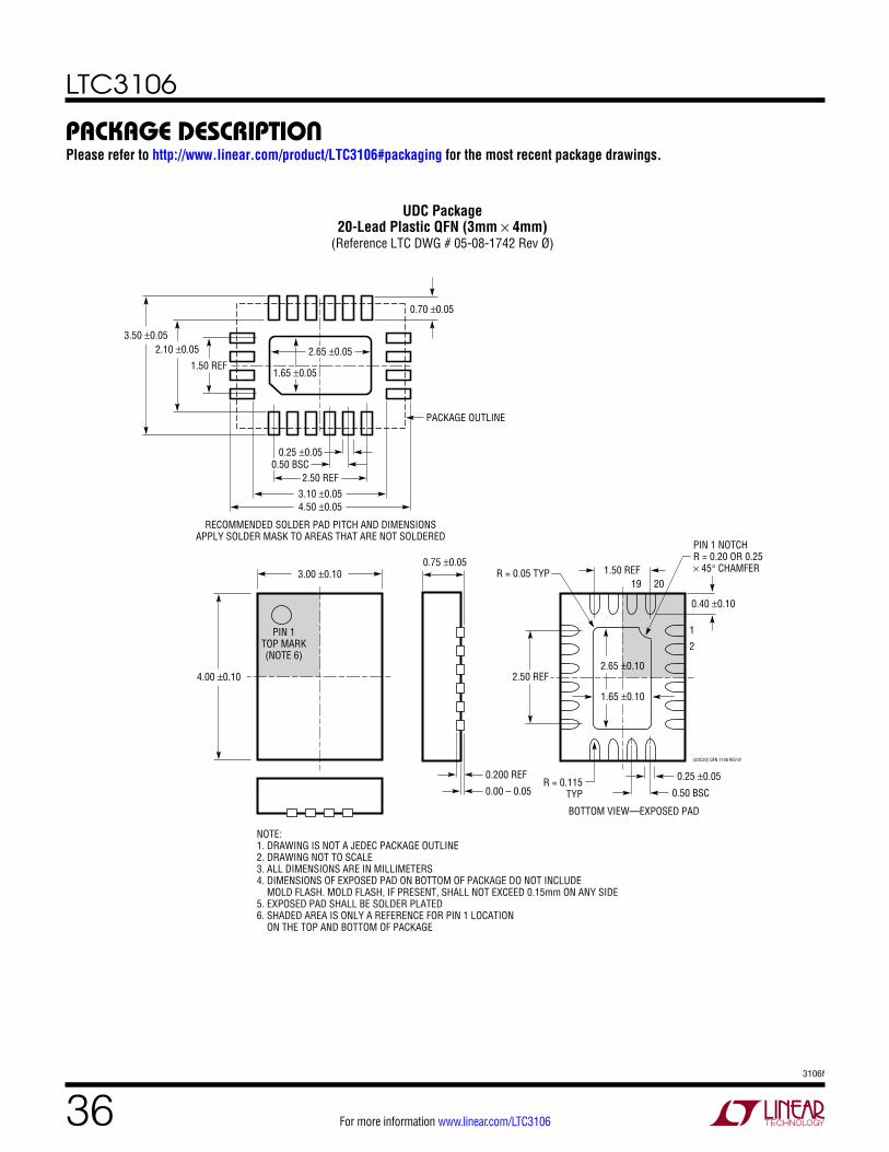
LTC3106
363106f
For more information www.linear.com/LTC3106
package DescripTionPlease refer to http://www.linear.com/product/LTC3106#packaging for the most recent package drawings.
3.00 ±0.10 1.50 REF
4.00 ±0.10
NOTE:1. DRAWING IS NOT A JEDEC PACKAGE OUTLINE2. DRAWING NOT TO SCALE3. ALL DIMENSIONS ARE IN MILLIMETERS4. DIMENSIONS OF EXPOSED PAD ON BOTTOM OF PACKAGE DO NOT INCLUDE MOLD FLASH. MOLD FLASH, IF PRESENT, SHALL NOT EXCEED 0.15mm ON ANY SIDE5. EXPOSED PAD SHALL BE SOLDER PLATED6. SHADED AREA IS ONLY A REFERENCE FOR PIN 1 LOCATION ON THE TOP AND BOTTOM OF PACKAGE
PIN 1TOP MARK(NOTE 6)
0.40 ±0.10
19 20
1
2
BOTTOM VIEW—EXPOSED PAD
2.50 REF
0.75 ±0.05
R = 0.115TYP
PIN 1 NOTCHR = 0.20 OR 0.25× 45° CHAMFER
0.25 ±0.05
0.50 BSC
0.200 REF
0.00 – 0.05
(UDC20) QFN 1106 REV Ø
RECOMMENDED SOLDER PAD PITCH AND DIMENSIONSAPPLY SOLDER MASK TO AREAS THAT ARE NOT SOLDERED
0.70 ±0.05
0.25 ±0.05
2.50 REF
3.10 ±0.054.50 ±0.05
1.50 REF
2.10 ±0.053.50 ±0.05
PACKAGE OUTLINE
R = 0.05 TYP
1.65 ±0.10
2.65 ±0.10
1.65 ±0.05
2.65 ±0.05
0.50 BSC
UDC Package20-Lead Plastic QFN (3mm × 4mm)
(Reference LTC DWG # 05-08-1742 Rev Ø)
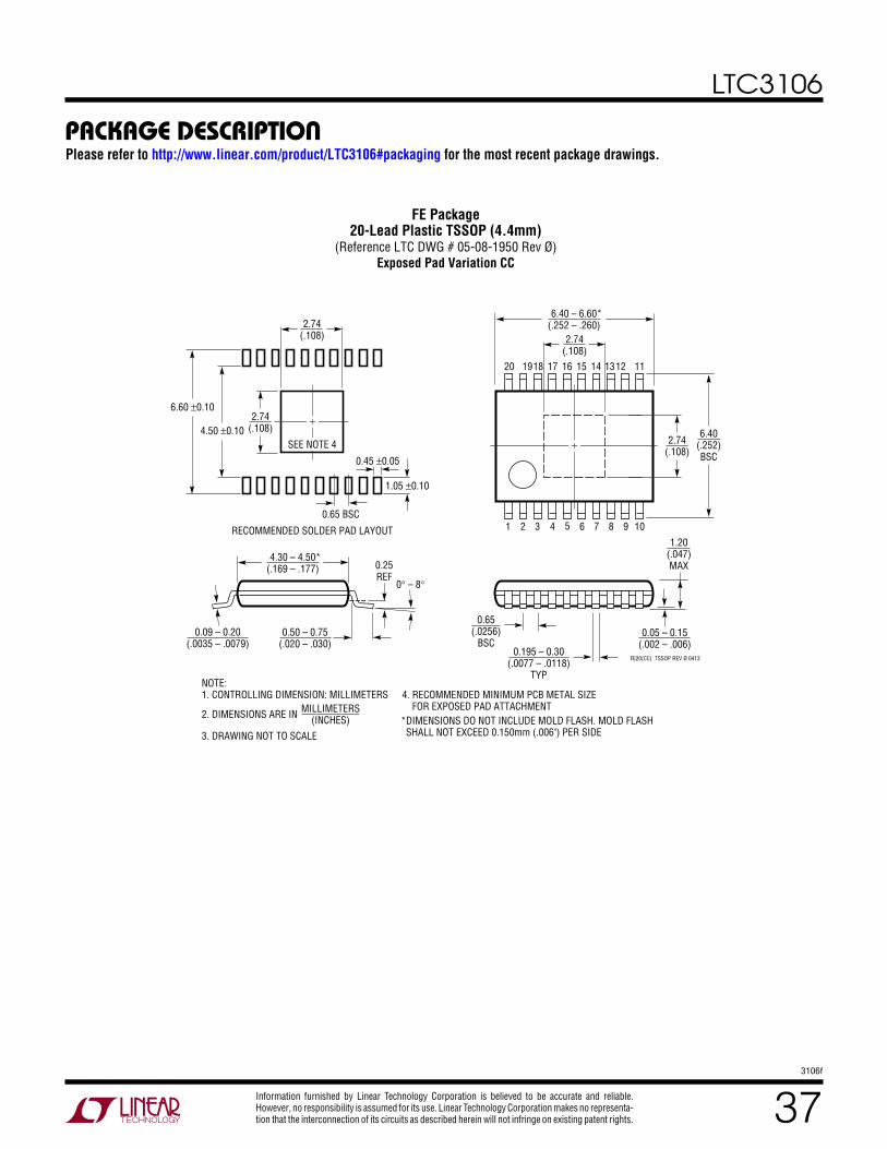
LTC3106
373106f
For more information www.linear.com/LTC3106
Information furnished by Linear Technology Corporation is believed to be accurate and reliable. However, no responsibility is assumed for its use. Linear Technology Corporation makes no representa-tion that the interconnection of its circuits as described herein will not infringe on existing patent rights.
package DescripTionPlease refer to http://www.linear.com/product/LTC3106#packaging for the most recent package drawings.
FE20(CC) TSSOP REV Ø 0413
0.09 – 0.20(.0035 – .0079)
0° – 8°
0.25REF
RECOMMENDED SOLDER PAD LAYOUT
0.50 – 0.75(.020 – .030)
4.30 – 4.50*(.169 – .177)
1 3 4 5 6 7 8 9 10
111214 13
6.40 – 6.60*(.252 – .260)
2.74(.108)
2.74(.108)
20 1918 17 16 15
1.20(.047)MAX
0.05 – 0.15(.002 – .006)
0.65(.0256)
BSC0.195 – 0.30
(.0077 – .0118)TYP
2
2.74(.108)
0.45 ±0.05
0.65 BSC
4.50 ±0.10
6.60 ±0.10
1.05 ±0.10
2.74(.108)
MILLIMETERS(INCHES) *DIMENSIONS DO NOT INCLUDE MOLD FLASH. MOLD FLASH
SHALL NOT EXCEED 0.150mm (.006") PER SIDE
NOTE:1. CONTROLLING DIMENSION: MILLIMETERS
2. DIMENSIONS ARE IN
3. DRAWING NOT TO SCALE
SEE NOTE 4
4. RECOMMENDED MINIMUM PCB METAL SIZE FOR EXPOSED PAD ATTACHMENT
6.40(.252)BSC
FE Package20-Lead Plastic TSSOP (4.4mm)
(Reference LTC DWG # 05-08-1950 Rev Ø)Exposed Pad Variation CC
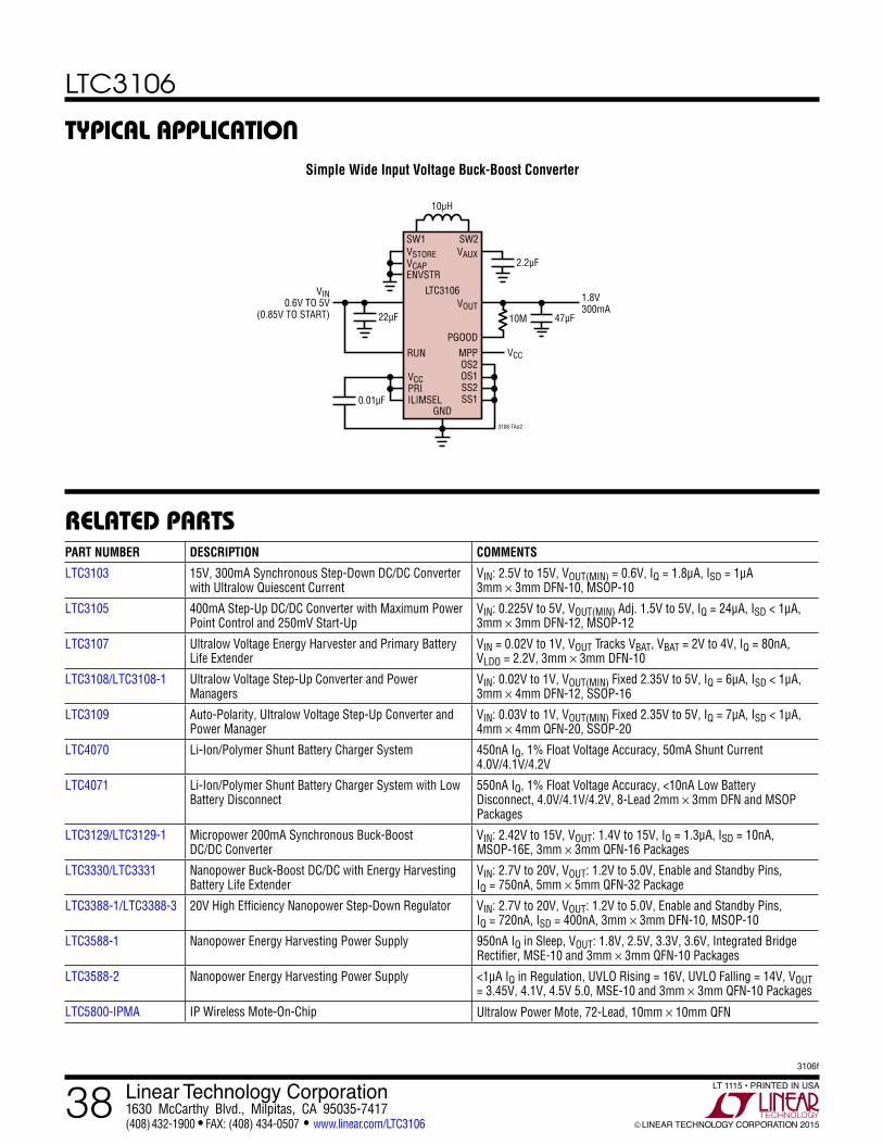
LTC3106
383106f
For more information www.linear.com/LTC3106 LINEAR TECHNOLOGY CORPORATION 2015
LT 1115 • PRINTED IN USALinear Technology Corporation1630 McCarthy Blvd., Milpitas, CA 95035-7417(408) 432-1900 FAX: (408) 434-0507 www.linear.com/LTC3106
relaTeD parTs
Typical applicaTion
PART NUMBER DESCRIPTION COMMENTS
LTC3103 15V, 300mA Synchronous Step-Down DC/DC Converter with Ultralow Quiescent Current
VIN: 2.5V to 15V, VOUT(MIN) = 0.6V, IQ = 1.8μA, ISD = 1μA 3mm × 3mm DFN-10, MSOP-10
LTC3105 400mA Step-Up DC/DC Converter with Maximum Power Point Control and 250mV Start-Up
VIN: 0.225V to 5V, VOUT(MIN) Adj. 1.5V to 5V, IQ = 24μA, ISD < 1μA, 3mm × 3mm DFN-12, MSOP-12
LTC3107 Ultralow Voltage Energy Harvester and Primary Battery Life Extender
VIN = 0.02V to 1V, VOUT Tracks VBAT, VBAT = 2V to 4V, IQ = 80nA, VLDO = 2.2V, 3mm × 3mm DFN-10
LTC3108/LTC3108-1 Ultralow Voltage Step-Up Converter and Power Managers
VIN: 0.02V to 1V, VOUT(MIN) Fixed 2.35V to 5V, IQ = 6μA, ISD < 1μA, 3mm × 4mm DFN-12, SSOP-16
LTC3109 Auto-Polarity, Ultralow Voltage Step-Up Converter and Power Manager
VIN: 0.03V to 1V, VOUT(MIN) Fixed 2.35V to 5V, IQ = 7μA, ISD < 1μA, 4mm × 4mm QFN-20, SSOP-20
LTC4070 Li-Ion/Polymer Shunt Battery Charger System 450nA IQ, 1% Float Voltage Accuracy, 50mA Shunt Current 4.0V/4.1V/4.2V
LTC4071 Li-Ion/Polymer Shunt Battery Charger System with Low Battery Disconnect
550nA IQ, 1% Float Voltage Accuracy, <10nA Low Battery Disconnect, 4.0V/4.1V/4.2V, 8-Lead 2mm × 3mm DFN and MSOP Packages
LTC3129/LTC3129-1 Micropower 200mA Synchronous Buck-Boost DC/DC Converter
VIN: 2.42V to 15V, VOUT: 1.4V to 15V, IQ = 1.3μA, ISD = 10nA, MSOP-16E, 3mm × 3mm QFN-16 Packages
LTC3330/LTC3331 Nanopower Buck-Boost DC/DC with Energy Harvesting Battery Life Extender
VIN: 2.7V to 20V, VOUT: 1.2V to 5.0V, Enable and Standby Pins, IQ = 750nA, 5mm × 5mm QFN-32 Package
LTC3388-1/LTC3388-3 20V High Efficiency Nanopower Step-Down Regulator VIN: 2.7V to 20V, VOUT: 1.2V to 5.0V, Enable and Standby Pins, IQ = 720nA, ISD = 400nA, 3mm × 3mm DFN-10, MSOP-10
LTC3588-1 Nanopower Energy Harvesting Power Supply 950nA IQ in Sleep, VOUT: 1.8V, 2.5V, 3.3V, 3.6V, Integrated Bridge Rectifier, MSE-10 and 3mm × 3mm QFN-10 Packages
LTC3588-2 Nanopower Energy Harvesting Power Supply <1μA IQ in Regulation, UVLO Rising = 16V, UVLO Falling = 14V, VOUT = 3.45V, 4.1V, 4.5V 5.0, MSE-10 and 3mm × 3mm QFN-10 Packages
LTC5800-IPMA IP Wireless Mote-On-Chip Ultralow Power Mote, 72-Lead, 10mm × 10mm QFN
10µH
VSTOREVCAPENVSTR
VCCPRIILIMSEL
VAUX
VOUT
MPPOS2OS1SS2SS1
GND
SW1 SW2
LTC3106
RUN
10M 47µF
1.8V300mA
VCC
3106 TAo2
2.2µF
22µF
0.01µF
PGOOD
VIN0.6V TO 5V
(0.85V TO START)
Simple Wide Input Voltage Buck-Boost Converter