Embed Size (px)
Citation preview
LTC2951-1/LTC2951-2
1295112fb
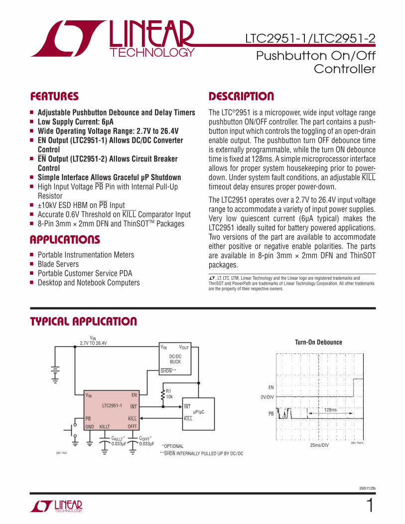
TYPICAL APPLICATION
APPLICATIONS
FEATURES DESCRIPTION
Pushbutton On/Off Controller
The LTC®2951 is a micropower, wide input voltage range pushbutton ON/OFF controller. The part contains a push-button input which controls the toggling of an open-drain enable output. The pushbutton turn OFF debounce time is externally programmable, while the turn ON debounce time is fixed at 128ms. A simple microprocessor interface allows for proper system housekeeping prior to power-down. Under system fault conditions, an adjustable KILL timeout delay ensures proper power-down.
The LTC2951 operates over a 2.7V to 26.4V input voltage range to accommodate a variety of input power supplies. Very low quiescent current (6µA typical) makes the LTC2951 ideally suited for battery powered applications. Two versions of the part are available to accommodate either positive or negative enable polarities. The parts are available in 8-pin 3mm × 2mm DFN and ThinSOT packages.
n Portable Instrumentation Metersn Blade Serversn Portable Customer Service PDAn Desktop and Notebook Computers
n Adjustable Pushbutton Debounce and Delay Timersn Low Supply Current: 6µA n Wide Operating Voltage Range: 2.7V to 26.4Vn EN Output (LTC2951-1) Allows DC/DC Converter
Controln EN Output (LTC2951-2) Allows Circuit Breaker
Controln Simple Interface Allows Graceful µP Shutdownn High Input Voltage PB Pin with Internal Pull-Up
Resistor n ±10kV ESD HBM on PB Input n Accurate 0.6V Threshold on KILL Comparator Inputn 8-Pin 3mm × 2mm DFN and ThinSOTTM Packages
Turn-On Debounce
L, LT, LTC, LTM, Linear Technology and the Linear logo are registered trademarks and ThinSOT and PowerPath are trademarks of Linear Technology Corporation. All other trademarks are the property of their respective owners.
VIN VOUT
VIN 2.7V TO 26.4V
EN
INT
KILL
INT
KILL
LTC2951-1
KILLT OFFT
DC/DCBUCK
µP/µC
R110k
2951 TA01
CKILLT*0.033µF
COFFT*0.033µF
PB
GND
VIN
SHDN**
*OPTIONAL
**SHDN INTERNALLY PULLED UP BY DC/DC
EN
2V/DIV
PB
25ms/DIV2951 TA01b
128ms
LTC2951-1/LTC2951-2
2295112fb
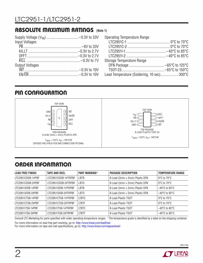
PIN CONFIGURATION
ABSOLUTE MAXIMUM RATINGSSupply Voltage (VIN) .................................. –0.3V to 33VInput Voltages PB .............................................................–6V to 33V KILLT .................................................... –0.3V to 2.7V OFFT ..................................................... –0.3V to 2.7V KILL ........................................................–0.3V to 7V Output Voltages INT ......................................................... –0.3V to 10V EN/EN .................................................... –0.3V to 10V
(Note 1)
Operating Temperature Range LTC2951C-1 ............................................. 0°C to 70°C LTC2951C-2 ............................................. 0°C to 70°C LTC2951I-1 ...........................................–40°C to 85°C LTC2951I-2 ..........................................–40°C to 85°CStorage Temperature Range
DFN Package ..................................... –65°C to 125°C TSOT-23 .............................................–65°C to 150°CLead Temperature (Soldering, 10 sec) ................... 300°C
TOP VIEW
DDB PACKAGE 8-LEAD (3mm × 2mm) PLASTIC DFN
5
6
7
8
9
4
3
2
1 INT
EN/EN
OFFT
KILL
GND
KILLT
PB
VIN
TJMAX = 125°C, θJA = 165°C/W
EXPOSED PAD (PIN 9) PCB GND CONNECTION OPTIONAL
VIN 1 PB 2
KILLT 3GND 4
8 KILL7 OFFT6 EN/EN5 INT
TOP VIEW
TS8 PACKAGE8-LEAD PLASTIC TSOT-23
TJMAX = 125°C, θJA = 140°C/W
ORDER INFORMATIONLEAD FREE FINISH TAPE AND REEL PART MARKING* PACKAGE DESCRIPTION TEMPERATURE RANGE
LTC2951CDDB-1#PBF LTC2951CDDB-1#TRPBF LBTB 8-Lead (3mm × 2mm) Plastic DFN 0°C to 70°C
LTC2951CDDB-2#PBF LTC2951CDDB-2#TRPBF LBTD 8-Lead (3mm × 2mm) Plastic DFN 0°C to 70°C
LTC2951IDDB-1#PBF LTC2951IDDB-1#TRPBF LBTB 8-Lead (3mm × 2mm) Plastic DFN –40°C to 85°C
LTC2951IDDB-2#PBF LTC2951IDDB-2#TRPBF LBTD 8-Lead (3mm × 2mm) Plastic DFN –40°C to 85°C
LTC2951CTS8-1#PBF LTC2951CTS8-1#TRPBF LTBTC 8-Lead Plastic TSOT 0°C to 70°C
LTC2951CTS8-2#PBF LTC2951CTS8-2#TRPBF LTBTF 8-Lead Plastic TSOT 0°C to 70°C
LTC2951ITS8-1#PBF LTC2951ITS8-1#TRPBF LTBTC 8-Lead Plastic TSOT –40°C to 85°C
LTC2951ITS8-2#PBF LTC2951ITS8-2#TRPBF LTBTF 8-Lead Plastic TSOT –40°C to 85°C
Consult LTC Marketing for parts specified with wider operating temperature ranges. *The temperature grade is identified by a label on the shipping container.For more information on lead free part marking, go to: http://www.linear.com/leadfree/ For more information on tape and reel specifications, go to: http://www.linear.com/tapeandreel/
LTC2951-1/LTC2951-2
3295112fb
The l denotes the specifications which apply over the full operating temperature range, otherwise specifications are at TA = 25°C. VIN = 2.7V to 26.4V, unless otherwise noted. (Note 2)
Note 1: Stresses beyond those listed under Absolute Maximum Ratings may cause permanent damage to the device. Exposure to any Absolute Maximum Rating condition for extended periods may affect device reliability and lifetime.Note 2: All currents into pins are positive; all voltages are referenced to GND unless otherwise noted.Note 3: The KILL turn-on blanking timer period is the waiting period immediately after the enable output is asserted. This blanking time allows sufficient time for the DC/DC converter and the µP to perform power-up tasks. The KILL and PB inputs are ignored during this period. If KILL remains low at the end of this time period, the enable output is released, thus turning off system power. This time delay does not include tDB,ON.
Note 4: The internal KILL turn-off delay (tKILL, OFF DELAY) is the default delay from the initiation of a power-off sequence (INT falling, KILL = high), to the release of the enable output. The additional, adjustable KILL turn-off delay (tKILL, OFF DELAY, ADDITIONAL) uses an optional external capacitor (CKILLT) to provide extra delay from INT falling to the release of the enable output. If the KILL input switches low at any time during KILL turn-off delay, enable is released, thus turning off system power.Note 5: The enable lockout time is designed to allow an application to properly power down such that the next power-up sequence starts from a consistent powered down configuration. PB is ignored during this lockout time. This time delay does not include tDB, ON.
ELECTRICAL CHARACTERISTICSSYMBOL PARAMETER CONDITIONS MIN TYP MAX UNITS
VIN Supply Voltage Range Steady-State Operation l 2.7 26.4 V
IIN VIN Supply Current System Power-On, VIN = 2.7V to 24V l 6 12 µA
VUVL VIN Undervoltage Lockout VIN Falling l 2.2 2.3 2.4 V
VUVL(HYST) VIN Undervoltage Lockout Hysteresis l 50 300 600 mV
Pushbutton, Enable (PB, EN/EN)
VPB(MIN, MAX) PB Voltage Range Single-Ended l –1 26.4 V
IPB PB Input Current 2.5V < VPB < 26.4V VPB = 1V VPB = 0.6V
l
l
l
–1 –3
–6 –9
±1 –12 –15
µA µA µA
VPB(VTH) PB Input Threshold PB Falling l 0.6 0.8 1 V
tEN/EN, Lockout EN/EN Lockout Time (Note 5) Enable Released → Enable Asserted l 200 256 325 ms
IEN/EN(LKG) EN/EN Leakage Current VEN/EN = 1V, Sink Current Off l ±0.1 µA
VEN/EN(VOL) EN/EN Voltage Output Low IEN/EN = 3mA l 0.11 0.4 V
VPB(VOC) PB Open-Circuit Voltage IPB = –1µA l 1 1.6 2 V
Timing Pins (KILLT, OFFT)
IKILLT, OFFT(PU) KILLT/OFFT Pull-Up Current VKILLT, OFFT = 0V l –2.4 –3 –3.6 µA
IKILLT, OFFT(PD) KILLT/OFFT Pull-Down Current VKILLT, OFFT = 1.3V l 2.4 3 3.6 µA
tDB, ON Turn-On Debounce Time PB Falling → Enable Asserted l 100 128 163 ms
tDB, OFF Internal Turn-Off Debounce Time OFFT Pin Float, PB Falling → INT Falling l 26 32 41 ms
tOFFT Additional Adjustable Turn-Off Time COFFT = 1500pF l 9 11.5 13.5 ms
µP Handshake Pins (INT, KILL)
IINT(LKG) INT Leakage Current VINT = 3V l ±1 µA
VINT(VOL) INT Output Voltage Low IINT = 3mA l 0.11 0.4 V
VKILL(TH) KILL Input Threshold Voltage KILL Falling l 0.57 0.6 0.63 V
VKILL(HYST) KILL Input Threshold Hysteresis l 10 30 50 mV
IKILL(LKG) KILL Leakage Current VKILL = 0.6V l ±0.1 µA
tKILL(PW) KILL Minimum Pulse Width l 30 µs
tKILL(PD) KILL Propagation Delay KILL Falling → Enable Released l 30 µs
tKILL, ON BLANK KILL Turn-On Blanking (Note 3) KILL = Low, Enable Asserted → Enable Released l 400 512 650 ms
tKILL, OFF DELAY Internal KILL Turn-Off Delay (Note 4) KILLT Pin Float, KILL = High, INT Asserted → Enable Released
l 100 128 163 ms
tKILL,OFF DELAY, ADDITIONAL
Additional Adjustable KILL Turn-Off Delay (Note 4)
CKILLT = 1500pF l 9 11.5 13.5 ms
LTC2951-1/LTC2951-2
4295112fb
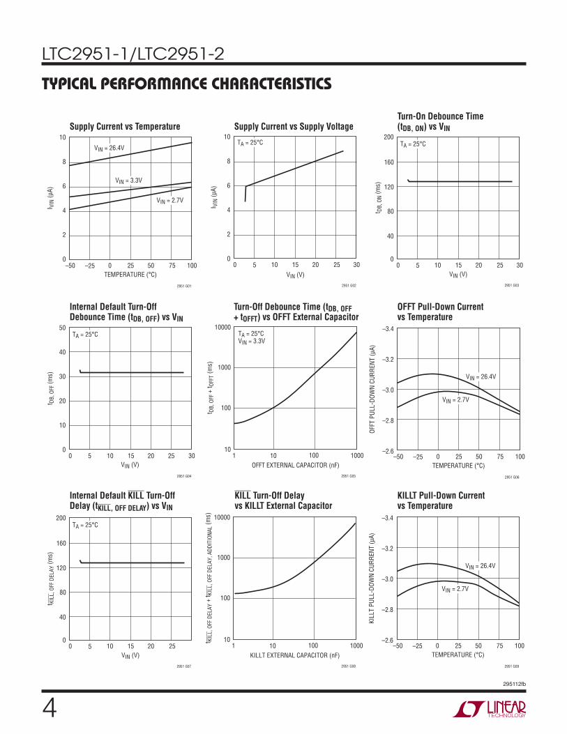
Supply Current vs Temperature
KILL Turn-Off Delay vs KILLT External Capacitor
Supply Current vs Supply Voltage
KILLT Pull-Down Current vs Temperature
Internal Default Turn-Off Debounce Time (tDB, OFF) vs VIN
Turn-Off Debounce Time (tDB, OFF + tOFFT) vs OFFT External Capacitor
OFFT Pull-Down Current vs Temperature
Internal Default KILL Turn-Off Delay (tKILL, OFF DELAY) vs VIN
Turn-On Debounce Time (tDB, ON) vs VIN
TEMPERATURE (°C)–50
I VIN
(µA)
10
8
6
4
2
0–25 0 25 50
2951 G01
75 100
VIN = 26.4V
VIN = 3.3V
VIN = 2.7V
0 5 10 15 20 25 30VIN (V)
I VIN
(µA)
10
8
6
4
2
0
2951 G02
TA = 25°C
2951 G03
VIN (V)0
0
t DB,
ON
(ms)
40
80
120
160
200
5 10 15 20 25 30
TA = 25°C
VIN (V)0
t DB,
OFF
(ms)
5 10 15 20
2951 G04
25 30
50
40
30
20
10
0
TA = 25°C
2951 G05
1
t DB,
OFF
+ t O
FFT
(ms)
100
1000
100010
10 100
10000TA = 25°CVIN = 3.3V
OFFT EXTERNAL CAPACITOR (nF)
2951 G06
TEMPERATURE (°C)–50 –25 0 25 50 75 100
OFFT
PUL
L-DO
WN
CURR
ENT
(µA)
–3.4
–3.2
–3.0
–2.8
–2.6
VIN = 26.4V
VIN = 2.7V
2951 G07
VIN (V)0
0
t KIL
L, O
FF D
ELAY
(ms)
40
80
120
160
200
5 10 15 20 25
TA = 25°C
1
t KIL
L, O
FF D
ELAY
+ t K
ILL,
OFF
DEL
AY, A
DDIT
IONA
L (m
s)
100
1000
1000
2951 G08
1010 100
10000
KILLT EXTERNAL CAPACITOR (nF) TEMPERATURE (°C)–50 –25 0 25 50 75 100
KILL
T PU
LL-D
OWN
CURR
ENT
(µA)
2951 G09
–3.4
–3.2
–3.0
–2.8
–2.6
VIN = 26.4V
VIN = 2.7V
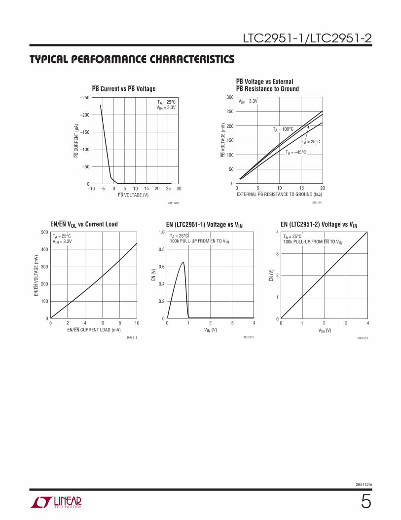
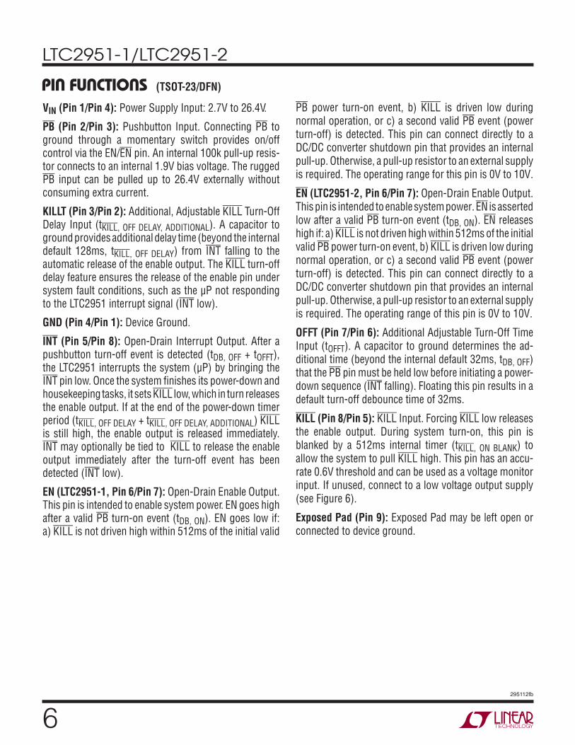
TYPICAL PERFORMANCE CHARACTERISTICS
LTC2951-1/LTC2951-2
5295112fb
PB Current vs PB VoltagePB Voltage vs External PB Resistance to Ground
EN/EN VOL vs Current Load EN (LTC2951-2) Voltage vs VINEN (LTC2951-1) Voltage vs VIN
PB C
URRE
NT (µ
A)
2951 G10
–10 0 10 20 30–5 5 15 25
–250
–200
–150
–100
–50
0
PB VOLTAGE (V)
TA = 25°CVIN = 3.3V
2951 G11
00
50
100
150
200
250
300
5 10 15 20
VIN = 3.3V
TA = 25°C
PB V
OLTA
GE (m
V)
EXTERNAL PB RESISTANCE TO GROUND (kΩ)
TA = –45°C
TA = 100°C
EN/EN CURRENT LOAD (mA)0
EN/E
N VO
LTAG
E (m
V)
500
400
300
200
100
08
2951 G12
2 4 6 10
TA = 25°CVIN = 3.3V
VIN (V)0
EN (V
)
4
2951 G13
1 2 3
TA = 25°C100k PULL-UP FROM EN TO VIN
1.0
0.8
0.6
0.4
0.2
0
EN (V
)
2951 G14
VIN (V)
0 41 2 3
4
3
2
1
0
TA = 25°C100k PULL-UP FROM EN TO VIN
TA = 25°C100k PULL-UP FROM EN TO VIN
TYPICAL PERFORMANCE CHARACTERISTICS
LTC2951-1/LTC2951-2
6295112fb
VIN (Pin 1/Pin 4): Power Supply Input: 2.7V to 26.4V.
PB (Pin 2/Pin 3): Pushbutton Input. Connecting PB to ground through a momentary switch provides on/off control via the EN/EN pin. An internal 100k pull-up resis-tor connects to an internal 1.9V bias voltage. The rugged PB input can be pulled up to 26.4V externally without consuming extra current.
KILLT (Pin 3/Pin 2): Additional, Adjustable KILL Turn-Off Delay Input (tKILL, OFF DELAY, ADDITIONAL). A capacitor to ground provides additional delay time (beyond the internal default 128ms, tKILL, OFF DELAY) from INT falling to the automatic release of the enable output. The KILL turn-off delay feature ensures the release of the enable pin under system fault conditions, such as the µP not responding to the LTC2951 interrupt signal (INT low).
GND (Pin 4/Pin 1): Device Ground.
INT (Pin 5/Pin 8): Open-Drain Interrupt Output. After a pushbutton turn-off event is detected (tDB, OFF + tOFFT), the LTC2951 interrupts the system (µP) by bringing the INT pin low. Once the system finishes its power-down and housekeeping tasks, it sets KILL low, which in turn releases the enable output. If at the end of the power-down timer period (tKILL, OFF DELAY + tKILL, OFF DELAY, ADDITIONAL) KILL is still high, the enable output is released immediately. INT may optionally be tied to KILL to release the enable output immediately after the turn-off event has been detected (INT low).
EN (LTC2951-1, Pin 6/Pin 7): Open-Drain Enable Output. This pin is intended to enable system power. EN goes high after a valid PB turn-on event (tDB, ON). EN goes low if: a) KILL is not driven high within 512ms of the initial valid
PB power turn-on event, b) KILL is driven low during normal operation, or c) a second valid PB event (power turn-off) is detected. This pin can connect directly to a DC/DC converter shutdown pin that provides an internal pull-up. Otherwise, a pull-up resistor to an external supply is required. The operating range for this pin is 0V to 10V.
EN (LTC2951-2, Pin 6/Pin 7): Open-Drain Enable Output. This pin is intended to enable system power. EN is asserted low after a valid PB turn-on event (tDB, ON). EN releases high if: a) KILL is not driven high within 512ms of the initial valid PB power turn-on event, b) KILL is driven low during normal operation, or c) a second valid PB event (power turn-off) is detected. This pin can connect directly to a DC/DC converter shutdown pin that provides an internal pull-up. Otherwise, a pull-up resistor to an external supply is required. The operating range of this pin is 0V to 10V.
OFFT (Pin 7/Pin 6): Additional Adjustable Turn-Off Time Input (tOFFT). A capacitor to ground determines the ad-ditional time (beyond the internal default 32ms, tDB, OFF) that the PB pin must be held low before initiating a power-down sequence (INT falling). Floating this pin results in a default turn-off debounce time of 32ms.
KILL (Pin 8/Pin 5): KILL Input. Forcing KILL low releases the enable output. During system turn-on, this pin is blanked by a 512ms internal timer (tKILL, ON BLANK) to allow the system to pull KILL high. This pin has an accu-rate 0.6V threshold and can be used as a voltage monitor input. If unused, connect to a low voltage output supply (see Figure 6).
Exposed Pad (Pin 9): Exposed Pad may be left open or connected to device ground.
(TSOT-23/DFN)PIN FUNCTIONS
LTC2951-1/LTC2951-2
7295112fb
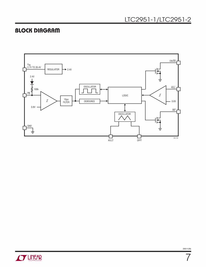
BLOCK DIAGRAM
LOGIC
OSCILLATOR
OSCILLATOR
DEBOUNCE
2.4V
2.4V
100k
VIN2.7V TO 26.4V
PB
GND
EN/EN
KILL
INT
KILLT OFFT
0.8V
0.6V
2951 BD
REGULATOR
10µsFILTER
LTC2951-1/LTC2951-2
8295112fb
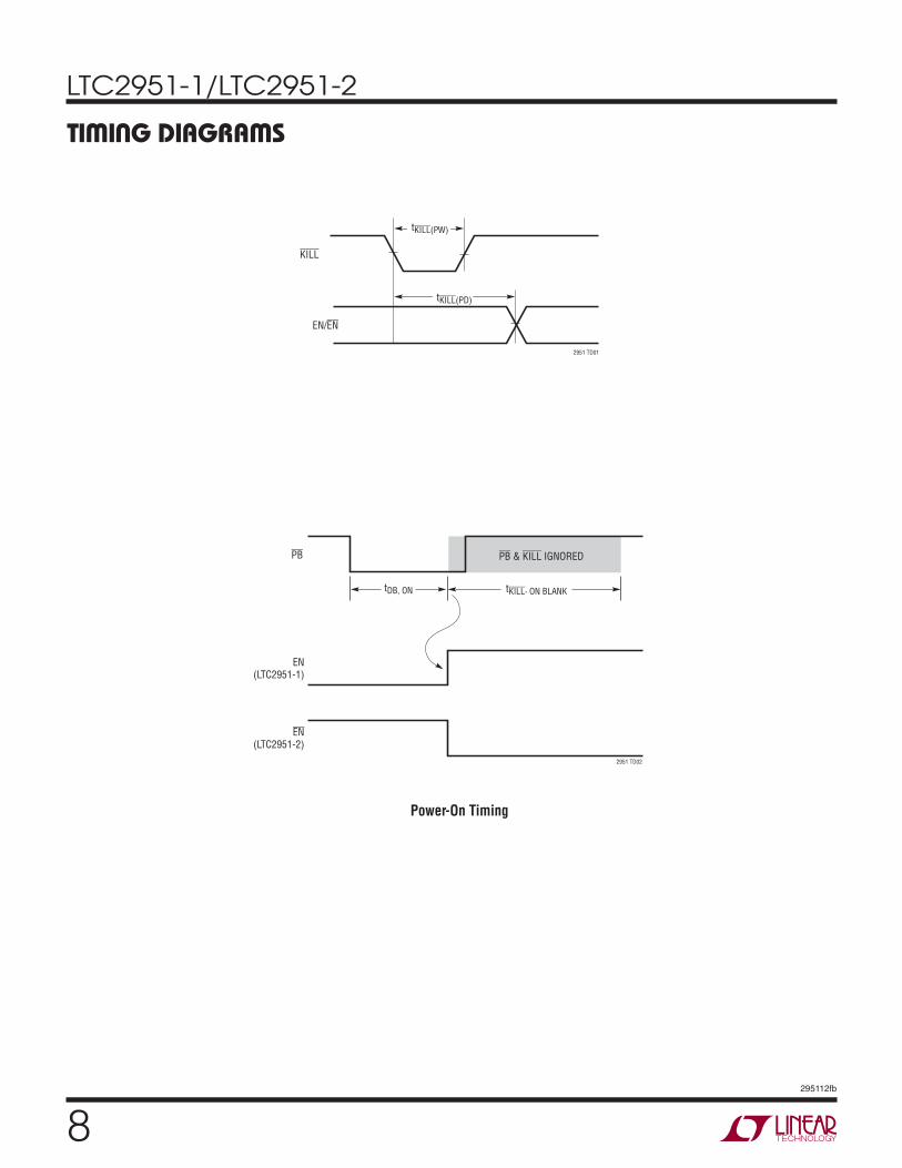
Power-On Timing
tDB, ON
PB PB & KILL IGNORED
EN(LTC2951-1)
EN(LTC2951-2)
tKILL, ON BLANK
2951 TD02
TIMING DIAGRAMS
KILL
EN/EN
tKILL(PD)
2951 TD01
tKILL(PW)
LTC2951-1/LTC2951-2
9295112fb
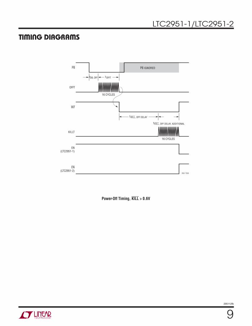
Power-Off Timing, KILL > 0.6V
PB
INT
OFFT
PB IGNORED
2951 TD03
16 CYCLES
16 CYCLES
EN(LTC2951-1)
KILLT
EN(LTC2951-2)
tKILL, OFF DELAY
tKILL, OFF DELAY, ADDITIONAL
tDB, OFF tOFFT
TIMING DIAGRAMS
LTC2951-1/LTC2951-2
10295112fb
Description
The LTC2951 is a low power (6µA), wide input voltage range (2.7V to 26.4V), pushbutton On/Off controller that can in-terface to a µP and a power supply. The part incorporates all the flexible timing needed to debounce the pushbutton input (PB). The LTC2951 also provides a simple interface (INT output, KILL input) to allow a system to power on and power off in a controlled manner. The wide input voltage range allows a system designer to operate from single cell to multi-cell battery stacks. Very low quiescent current makes the LTC2951 ideal for continuously monitoring the on/off pushbutton of a handheld device.
Turn-On
When power is first applied to the LTC2951, the part initial-izes the output pins. Any DC/DC converters connected to the EN/EN pin will, therefore, be off. To assert the enable output, PB must be held low for a minimum of 128ms (tDB, ON).
Once the enable output is asserted, any DC/DC converters connected to this pin are turned on. The KILL input from the µP is ignored during the succeeding 512ms blanking time (tKILL, ON BLANK). This blanking time represents the maximum time required to power up the DC/DC converter and the µP. If KILL is not brought high during this 512ms time window, the enable output is released. The assumption is that 512ms is sufficient time for the system to power up.
Turn-Off
To initiate a power-off sequence, PB must be held low for a minimum of 32ms (tDB, OFF). Additional turn-off debounce time may be added via an optional capacitor connected to the OFFT pin (tOFFT). The following equation describes the additional time that PB must be held low to initiate a power-off sequence. COFFT is the OFFT external capacitor:
COFFT = 1.56E-4 [µF/ms] • (tOFFT – 1ms)
Once PB has been validly pressed, INT is switched low. This alerts the µP to perform its power-down and house-keeping tasks.
KILL Turn-Off Delay
The LTC2951 provides a failsafe feature that allows the user to turn off system power (via PB) under system fault conditions. During a normal power-down sequence, the LTC2951 first interrupts the µP by setting INT low. The µP then performs power-down and housekeeping tasks and drives KILL low when done. The LTC2951 releases the enable output, thus turning off system power. The KILL turn-off timer starts when INT is driven low. If the µP fails to respond during this timeout period, the enable output will automatically release. The default power-down timeout period is 128ms (tKILL, OFF DELAY), which can be extended by placing an optional capacitor on the KILLT pin (tKILL, OFF DELAY, ADDITIONAL). The following equation describes the additional power-down timeout period. CKILLT is the KILLT external capacitor:
CKILLT = 1.56e-4 [µF/ms] • (tKILL, OFF DELAY, ADDITIONAL – 1ms)
Note that KILL can be driven low (thereby releasing the enable output) at any time after tKILL, ON BLANK period.
APPLICATIONS INFORMATION
LTC2951-1/LTC2951-2
11295112fb
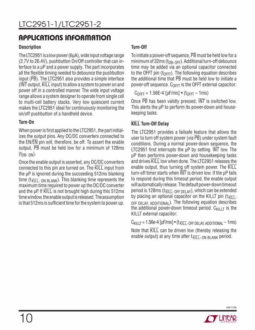
Figure 1. Simplified Power-On/-Off Sequence for LTC2951-1
Simplified Power-On/-Off Sequence
Figure 1 shows a simplified LTC2951-1 power-on and power-off sequence. A high to low transition on PB (t1) initiates the power-on sequence. This diagram does not show any bounce on PB . In order to assert the enable output, the PB pin must stay low continuously (PB high resets timers) for 128ms (t2–t1). Once EN goes high (t2), an internal 512ms blanking timer is started. This blank-ing timer is designed to give sufficient time for the DC/DC converter to reach its final voltage, and to allow the µP enough time to perform power-on tasks.
The KILL pin must be pulled high within 512ms of the EN pin going high. Failure to do so results in the EN
APPLICATIONS INFORMATION
PB
OFFT
EN
KILL
INT
PB & KILL IGNORED PB IGNORED
2951 F01
tDB, ON tKILL, ON BLANK
t1 t2 t3 t4 t5 t6 t7
tDB, OFF
tOFFT
< tKILL, OFF DELAY
pin going low 512ms after it went high. (EN = low, see Figure 2). Note that the LTC2951 does not sample KILL and PB until after the 512ms internal timer has expired. The reason PB is ignored is to ensure that the system is not forced off while powering on. Once the 512ms timer expires (t4), the release of the PB pin is then debounced with an internal 32ms timer. The system has now properly powered on and the LTC2951 monitors PB and KILL (for a turnoff command) while consuming only 6µA of supply current.
A high to low transition on PB (t5) initiates the power-off sequence. PB must stay low continuously (PB high resets debounce timer) for a period controlled by the default 32ms
LTC2951-1/LTC2951-2
12295112fb
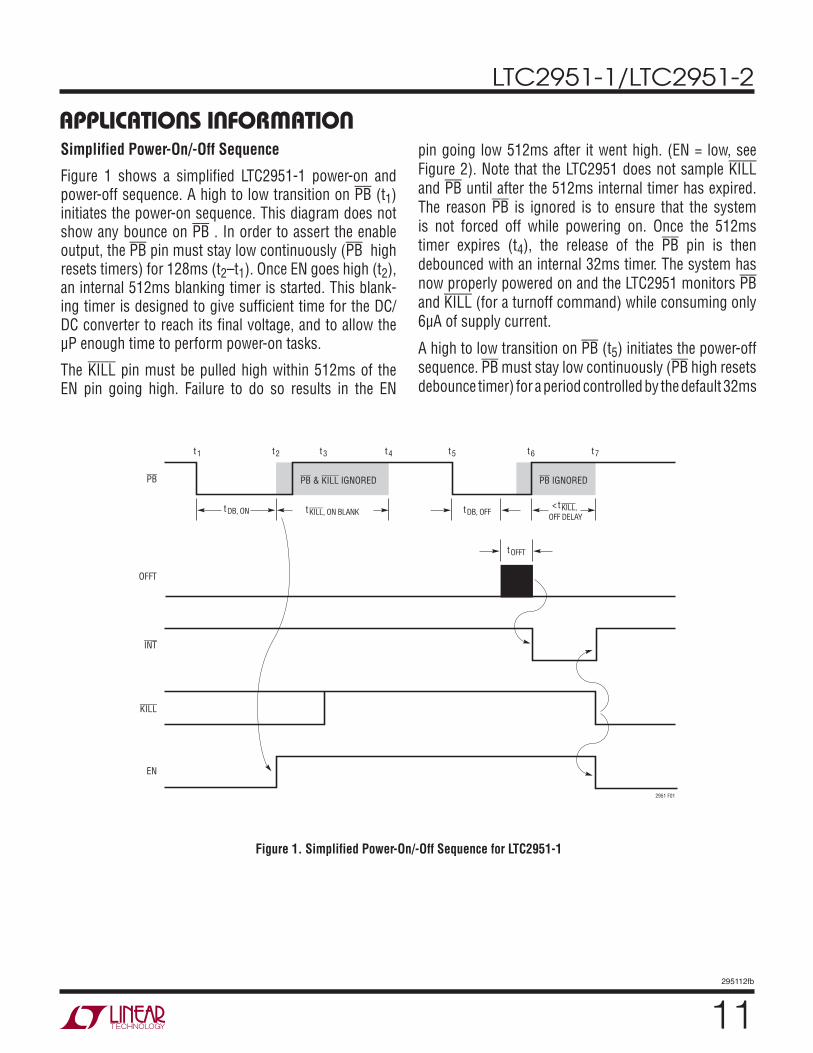
Figure 2. Aborted Power-On Sequence for LTC2951-1
and the external OFFT capacitor (t6–t5). At the completion of the OFFT timing (t6), an interrupt (INT) is set, signify-ing that EN will be switched low after the KILL turn-off (tKILL, OFF DELAY + tKILL, OFF DELAY, ADDITIONAL) timeout period. Once a system has finished performing its power-down operations, it can set KILL low (t7) and thus imme-diately set EN low, terminating the KILL turn-off timer. The release of the PB pin is then debounced with an internal 32ms timer.
The system is now in its reset state: where the LTC2951 is in low power mode (6µA). PB is monitored for a high to low transition.
Figure 3. µP Turns Off Power (LTC2951-1)
APPLICATIONS INFORMATION
PB
KILL
POWER-ONTIMING
EN
512msINTERNAL
TIMER
POWERTURNED OFF
2951 F02
µP FAILED TO SETKILL HIGH
tDB, ON
tABORT
PB & KILL IGNOREDPB
EN
DC/DCTURNS OFF
2951 F03
KILL XXX DON’T CARE
µP SETSKILL LOW
tKILL
Aborted Power-On Sequence
The power-on sequence is aborted when the KILL remains low after the end of the 512ms blanking time. Figure 2 is a simplified version of an aborted power-on sequence. At time tABORT, since KILL is still low, EN pulls low (thus turning off the DC/DC converter).
µP Turns Off Power During Normal Operation
Once the system has powered on and is operating nor-mally, the µP can turn off power by setting KILL low, as shown in Figure 3. At time tKILL, KILL is set low by the µP. This immediately pulls EN low, thus turning off the DC/DC converter.
LTC2951-1/LTC2951-2
13295112fb
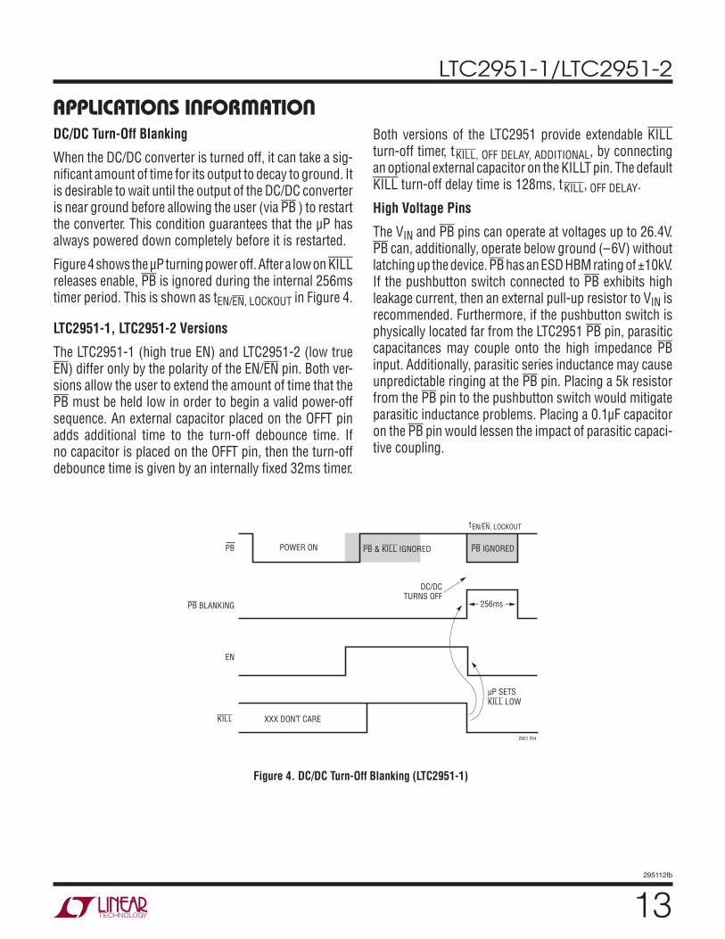
DC/DC Turn-Off Blanking
When the DC/DC converter is turned off, it can take a sig-nificant amount of time for its output to decay to ground. It is desirable to wait until the output of the DC/DC converter is near ground before allowing the user (via PB ) to restart the converter. This condition guarantees that the µP has always powered down completely before it is restarted.
Figure 4 shows the µP turning power off. After a low on KILL releases enable, PB is ignored during the internal 256ms timer period. This is shown as tEN/EN, LOCKOUT in Figure 4.
LTC2951-1, LTC2951-2 Versions
The LTC2951-1 (high true EN) and LTC2951-2 (low true EN) differ only by the polarity of the EN/EN pin. Both ver-sions allow the user to extend the amount of time that the PB must be held low in order to begin a valid power-off sequence. An external capacitor placed on the OFFT pin adds additional time to the turn-off debounce time. If no capacitor is placed on the OFFT pin, then the turn-off debounce time is given by an internally fixed 32ms timer.
Both versions of the LTC2951 provide extendable KILL turn-off timer, tKILL, OFF DELAY, ADDITIONAL, by connecting an optional external capacitor on the KILLT pin. The default KILL turn-off delay time is 128ms, tKILL, OFF DELAY.
High Voltage Pins
The VIN and PB pins can operate at voltages up to 26.4V. PB can, additionally, operate below ground (–6V) without latching up the device. PB has an ESD HBM rating of ±10kV. If the pushbutton switch connected to PB exhibits high leakage current, then an external pull-up resistor to VIN is recommended. Furthermore, if the pushbutton switch is physically located far from the LTC2951 PB pin, parasitic capacitances may couple onto the high impedance PB input. Additionally, parasitic series inductance may cause unpredictable ringing at the PB pin. Placing a 5k resistor from the PB pin to the pushbutton switch would mitigate parasitic inductance problems. Placing a 0.1µF capacitor on the PB pin would lessen the impact of parasitic capaci-tive coupling.
APPLICATIONS INFORMATION
Figure 4. DC/DC Turn-Off Blanking (LTC2951-1)
PB & KILL IGNOREDPB PB IGNORED
EN
KILL
PB BLANKING
XXX DON’T CARE
256ms
POWER ON
2951 F04
DC/DCTURNS OFF
tEN/EN, LOCKOUT
µP SETSKILL LOW
LTC2951-1/LTC2951-2
14295112fb
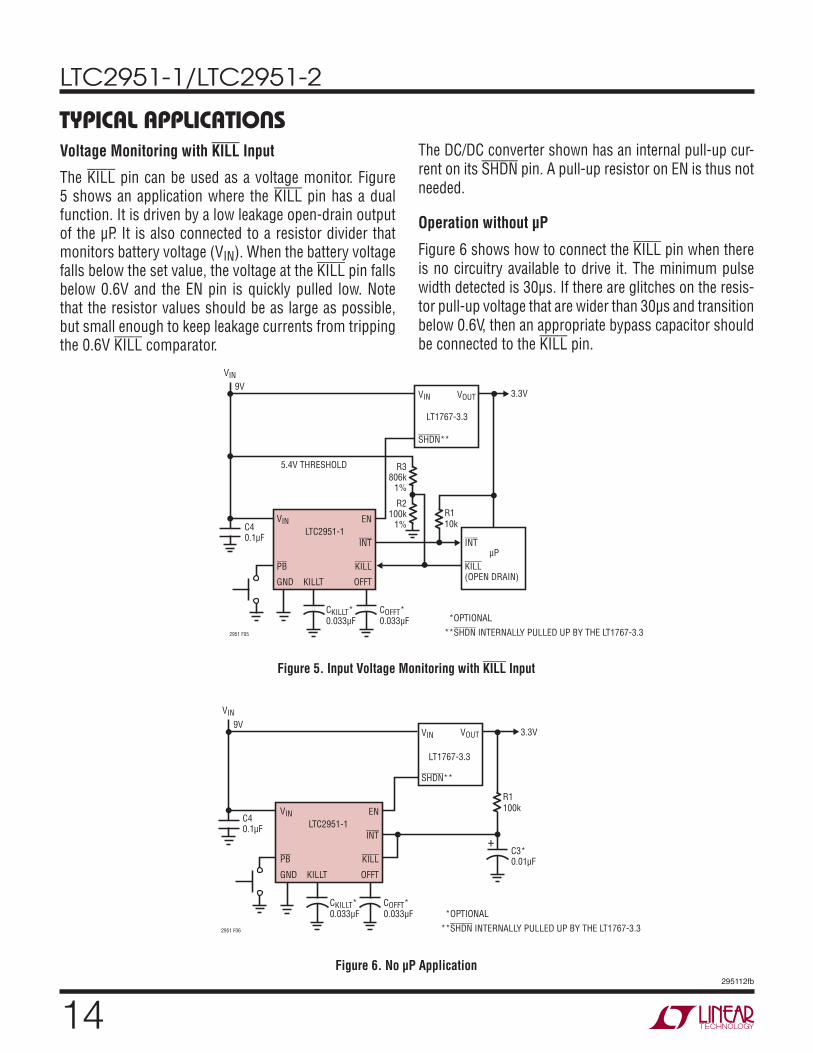
TYPICAL APPLICATIONSVoltage Monitoring with KILL Input
The KILL pin can be used as a voltage monitor. Figure 5 shows an application where the KILL pin has a dual function. It is driven by a low leakage open-drain output of the µP. It is also connected to a resistor divider that monitors battery voltage (VIN). When the battery voltage falls below the set value, the voltage at the KILL pin falls below 0.6V and the EN pin is quickly pulled low. Note that the resistor values should be as large as possible, but small enough to keep leakage currents from tripping the 0.6V KILL comparator.
The DC/DC converter shown has an internal pull-up cur-rent on its SHDN pin. A pull-up resistor on EN is thus not needed.
Operation without µP
Figure 6 shows how to connect the KILL pin when there is no circuitry available to drive it. The minimum pulse width detected is 30µs. If there are glitches on the resis-tor pull-up voltage that are wider than 30µs and transition below 0.6V, then an appropriate bypass capacitor should be connected to the KILL pin.
Figure 5. Input Voltage Monitoring with KILL Input
Figure 6. No µP Application
PB
VIN
SHDN**
VIN
VOUT
EN
INT
KILL
INT
KILL(OPEN DRAIN)
LTC2951-1
GND OFFT
LT1767-3.3
µP
9V
R110k
3.3V
2951 F05
C40.1µF
R3806k
1%
R2100k
1%
5.4V THRESHOLD
*OPTIONAL
**SHDN INTERNALLY PULLED UP BY THE LT1767-3.3
VIN
CKILLT*0.033µF
COFFT*0.033µF
KILLT
VIN
VIN
VOUT
LT1767-3.3
9V3.3V
R1100k
C3*0.01µF
2951 F06
+
C40.1µF
C3*0.01µFPB
EN
INT
KILL
LTC2951-1
GND KILLT OFFT
VIN
CKILLT*0.033µF
COFFT*0.033µF
SHDN**
*OPTIONAL
**SHDN INTERNALLY PULLED UP BY THE LT1767-3.3
LTC2951-1/LTC2951-2
15295112fb
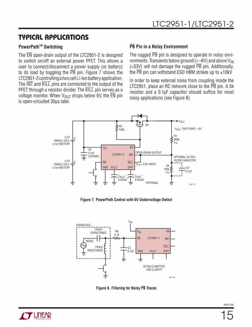
PowerPathTM Switching
The EN open-drain output of the LTC2951-2 is designed to switch on/off an external power PFET. This allows a user to connect/disconnect a power supply (or battery) to its load by toggling the PB pin. Figure 7 shows the LTC2951-2 controlling a two cell Li-Ion battery application. The INT and KILL pins are connected to the output of the PFET through a resistor divider. The KILL pin serves as a voltage monitor. When VOUT drops below 6V, the EN pin is open-circuited 30µs later.
Figure 7. PowerPath Control with 6V Undervoltage Detect
Figure 8. Filtering for Noisy PB Traces
PB Pin in a Noisy Environment
The rugged PB pin is designed to operate in noisy envi-ronments. Transients below ground (>–6V) and above VIN (<33V) will not damage the rugged PB pin. Additionally, the PB pin can withstand ESD HBM strikes up to ±10kV.
In order to keep external noise from coupling inside the LTC2951, place an RC network close to the PB pin. A 5k resistor and a 0.1µF capacitor should suffice for most noisy applications (see Figure 8).
TYPICAL APPLICATIONS
VOUT
R1909k1%
R4100k
1%
C3*0.1µF
2951 F07
C40.1µFCERAMIC
*OPTIONAL
OPEN-DRAIN OUTPUT
VTH = 0.6V INPUT
R5100k
M1
+4.2VSINGLE-CELL
Li-Ion BATTERY
+4.2VSINGLE-CELL
Li-Ion BATTERY
OPTIONAL GLITCHFILTER CAPACITOR
VOUT, TRIP POINT = 6V
PB
EN
INT
KILL
LTC2951-2
GND OFFT
VIN
CKILLT*0.033µF
COFFT*0.033µF
KILLT
PB LTC2951-1
GND
R65.1k
2951 F08
TRACECAPACITANCE
PARASITICS
C50.1µF
DETAILS OMITTED FOR CLARITY
TRACEINDUCTANCE
NOISE
EN
INT
KILL
OFFT
VIN
KILLT
VIN
LTC2951-1/LTC2951-2
16295112fb
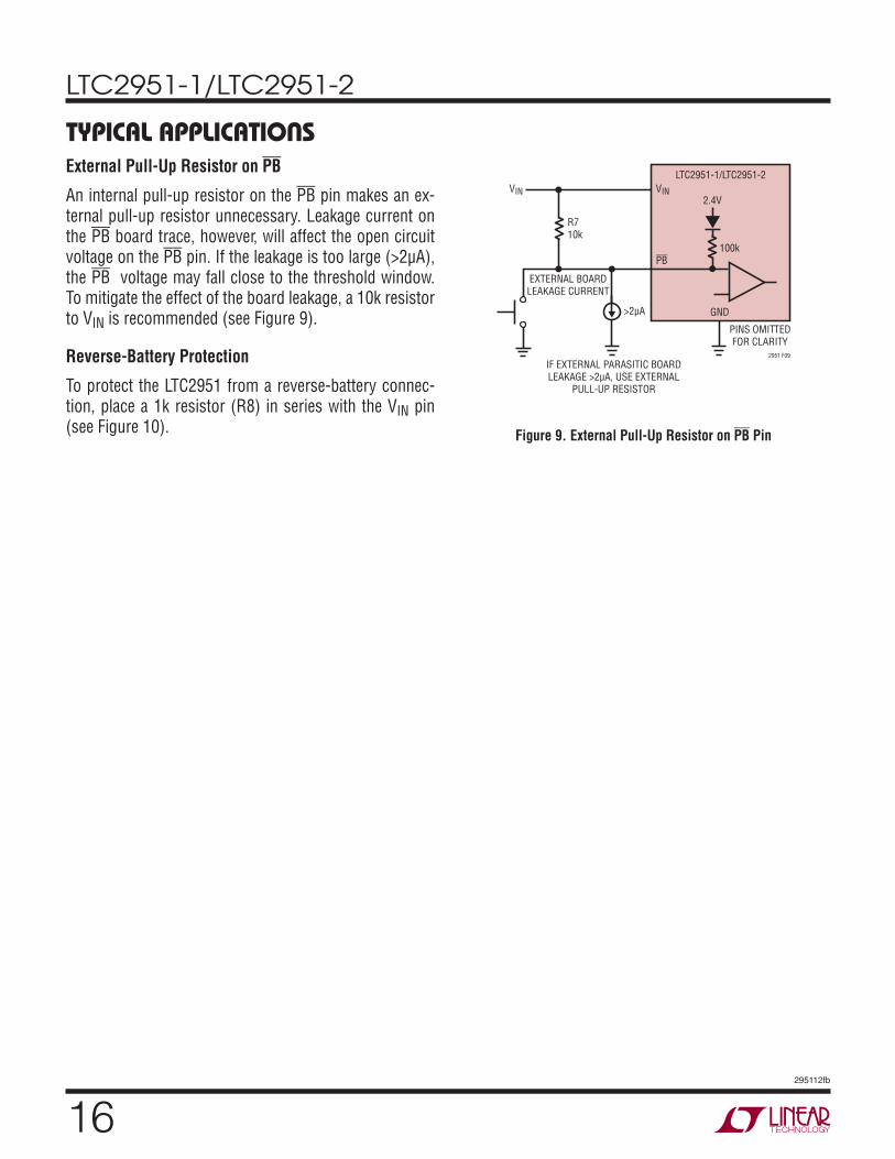
External Pull-Up Resistor on PB
An internal pull-up resistor on the PB pin makes an ex-ternal pull-up resistor unnecessary. Leakage current on the PB board trace, however, will affect the open circuit voltage on the PB pin. If the leakage is too large (>2µA), the PB voltage may fall close to the threshold window. To mitigate the effect of the board leakage, a 10k resistor to VIN is recommended (see Figure 9).
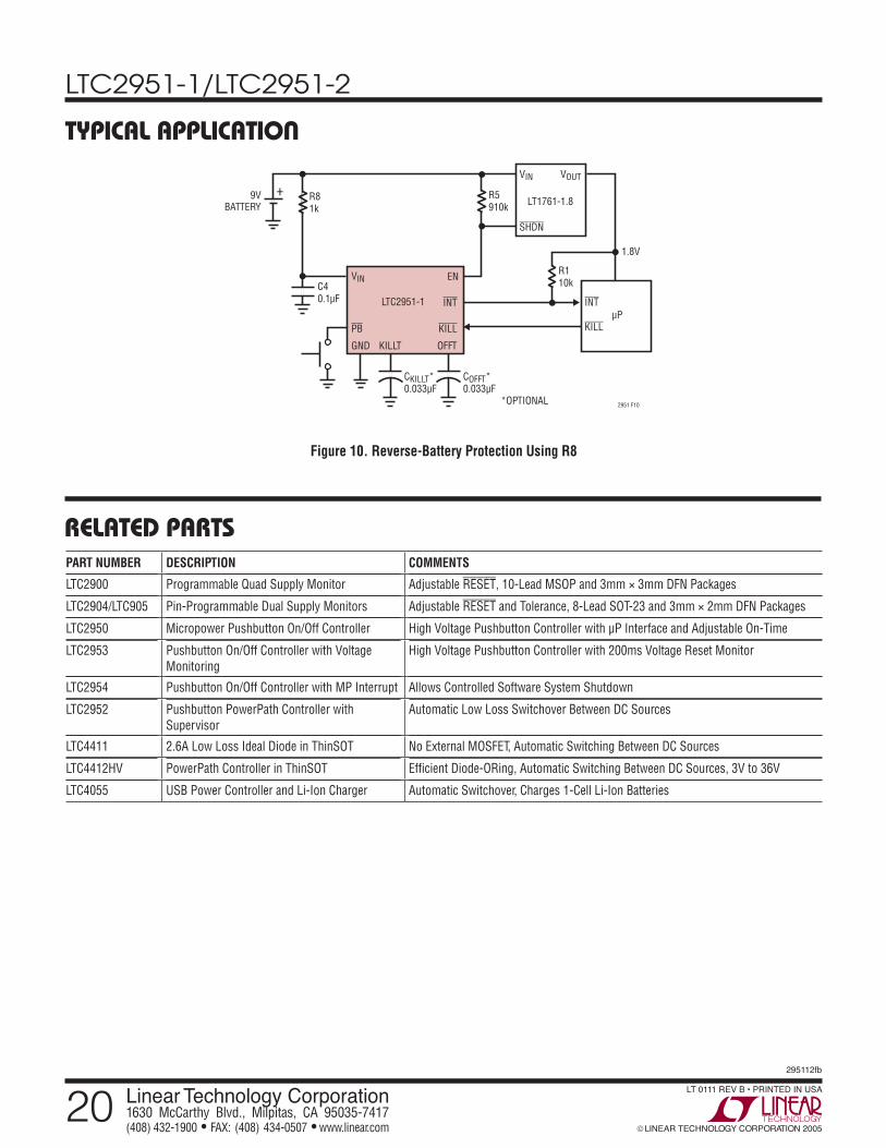
Reverse-Battery Protection
To protect the LTC2951 from a reverse-battery connec-tion, place a 1k resistor (R8) in series with the VIN pin (see Figure 10). Figure 9. External Pull-Up Resistor on PB Pin
TYPICAL APPLICATIONS
PB
LTC2951-1/LTC2951-2
GND
EXTERNAL BOARDLEAKAGE CURRENT
100k
2.4V
R710k
2951 F09
>2µA
PINS OMITTEDFOR CLARITY
IF EXTERNAL PARASITIC BOARDLEAKAGE >2µA, USE EXTERNAL
PULL-UP RESISTOR
VINVIN
LTC2951-1/LTC2951-2
17295112fb
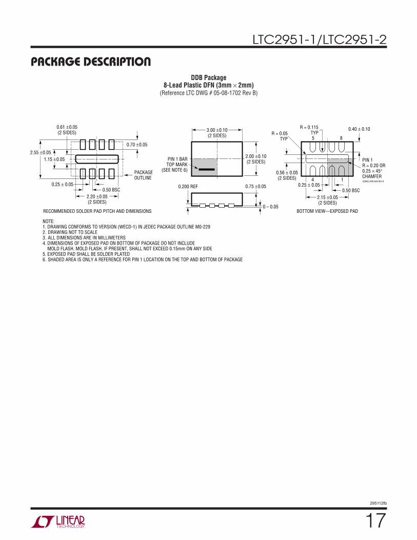
PACKAGE DESCRIPTION
2.00 ±0.10(2 SIDES)
NOTE:1. DRAWING CONFORMS TO VERSION (WECD-1) IN JEDEC PACKAGE OUTLINE M0-229 2. DRAWING NOT TO SCALE 3. ALL DIMENSIONS ARE IN MILLIMETERS4. DIMENSIONS OF EXPOSED PAD ON BOTTOM OF PACKAGE DO NOT INCLUDE MOLD FLASH. MOLD FLASH, IF PRESENT, SHALL NOT EXCEED 0.15mm ON ANY SIDE5. EXPOSED PAD SHALL BE SOLDER PLATED6. SHADED AREA IS ONLY A REFERENCE FOR PIN 1 LOCATION ON THE TOP AND BOTTOM OF PACKAGE
0.40 ± 0.10
BOTTOM VIEW—EXPOSED PAD
0.56 ± 0.05(2 SIDES)
0.75 ±0.05
R = 0.115TYPR = 0.05
TYP
2.15 ±0.05(2 SIDES)
3.00 ±0.10(2 SIDES)
14
85
PIN 1 BARTOP MARK
(SEE NOTE 6)
0.200 REF
0 – 0.05
(DDB8) DFN 0905 REV B
0.25 ± 0.05
2.20 ±0.05(2 SIDES)
RECOMMENDED SOLDER PAD PITCH AND DIMENSIONS
0.61 ±0.05(2 SIDES)
1.15 ±0.05
0.70 ±0.05
2.55 ±0.05
PACKAGEOUTLINE
0.25 ± 0.050.50 BSC
PIN 1R = 0.20 OR0.25 × 45°CHAMFER
0.50 BSC
DDB Package8-Lead Plastic DFN (3mm × 2mm)
(Reference LTC DWG # 05-08-1702 Rev B)
LTC2951-1/LTC2951-2
18295112fb
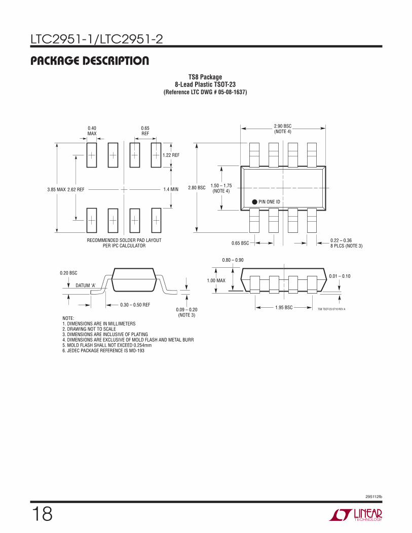
TS8 Package8-Lead Plastic TSOT-23
(Reference LTC DWG # 05-08-1637)
1.50 – 1.75(NOTE 4)
2.80 BSC
0.22 – 0.36 8 PLCS (NOTE 3)
DATUM ‘A’
0.09 – 0.20(NOTE 3)
TS8 TSOT-23 0710 REV A
2.90 BSC(NOTE 4)
0.65 BSC
1.95 BSC
0.80 – 0.90
1.00 MAX0.01 – 0.10
0.20 BSC
0.30 – 0.50 REF
PIN ONE ID
NOTE:1. DIMENSIONS ARE IN MILLIMETERS2. DRAWING NOT TO SCALE3. DIMENSIONS ARE INCLUSIVE OF PLATING4. DIMENSIONS ARE EXCLUSIVE OF MOLD FLASH AND METAL BURR5. MOLD FLASH SHALL NOT EXCEED 0.254mm6. JEDEC PACKAGE REFERENCE IS MO-193
3.85 MAX
0.40MAX
0.65REF
RECOMMENDED SOLDER PAD LAYOUTPER IPC CALCULATOR
1.4 MIN2.62 REF
1.22 REF
PACKAGE DESCRIPTION
LTC2951-1/LTC2951-2
19295112fb
Information furnished by Linear Technology Corporation is believed to be accurate and reliable. However, no responsibility is assumed for its use. Linear Technology Corporation makes no representa-tion that the interconnection of its circuits as described herein will not infringe on existing patent rights.
REVISION HISTORYREV DATE DESCRIPTION PAGE NUMBER
B 01/11 Revised Features and Typical Application 1
Updated Pin Configuration 2
Revised Electrical Characteristics section 3
Revised Pin Functions section 6
Revised Block Diagram 7
Minor edit to Figure 1 11
Added C3 to Figure 6 14
Updated Figure 8 15
Updated Related Parts 20
(Revision history begins at Rev B)
LTC2951-1/LTC2951-2
20295112fb
Linear Technology Corporation1630 McCarthy Blvd., Milpitas, CA 95035-7417 (408) 432-1900 ● FAX: (408) 434-0507 ● www.linear.com LINEAR TECHNOLOGY CORPORATION 2005
LT 0111 REV B • PRINTED IN USA
SHDN
INT
KILL
LT1761-1.8
R110k
R81k
R5910k
2951 F10
C40.1µF
+
µP
1.8V
9VBATTERY
PB
EN
INT
KILL
LTC2951-1
GND KILLT OFFT
CKILLT*0.033µF
VIN
COFFT*0.033µF
*OPTIONAL
VIN VOUT
Figure 10. Reverse-Battery Protection Using R8
TYPICAL APPLICATION
RELATED PARTSPART NUMBER DESCRIPTION COMMENTS
LTC2900 Programmable Quad Supply Monitor Adjustable RESET, 10-Lead MSOP and 3mm × 3mm DFN Packages
LTC2904/LTC905 Pin-Programmable Dual Supply Monitors Adjustable RESET and Tolerance, 8-Lead SOT-23 and 3mm × 2mm DFN Packages
LTC2950 Micropower Pushbutton On/Off Controller High Voltage Pushbutton Controller with µP Interface and Adjustable On-Time
LTC2953 Pushbutton On/Off Controller with Voltage Monitoring
High Voltage Pushbutton Controller with 200ms Voltage Reset Monitor
LTC2954 Pushbutton On/Off Controller with MP Interrupt Allows Controlled Software System Shutdown
LTC2952 Pushbutton PowerPath Controller with Supervisor
Automatic Low Loss Switchover Between DC Sources
LTC4411 2.6A Low Loss Ideal Diode in ThinSOT No External MOSFET, Automatic Switching Between DC Sources
LTC4412HV PowerPath Controller in ThinSOT Efficient Diode-ORing, Automatic Switching Between DC Sources, 3V to 36V
LTC4055 USB Power Controller and Li-Ion Charger Automatic Switchover, Charges 1-Cell Li-Ion Batteries


![CR-1 : @TAWAS B LIB.TAWAS B(SCH 1):PAGE1 TAWASnotebookschematic.org/data/NOTEBOOK/attachments/SC... · resume gp[6] gp[7] gp[8] gp[9] 3.3v 3.3v 3.3v 3.3v gp[23] gp[24] gp[25] gp[26]](https://img.pdfslide.us/doc/110x75/5f812ff679030c23f20de0bd/cr-1-tawas-b-libtawas-bsch-1page1-ta-resume-gp6-gp7-gp8-gp9-33v.jpg)