Embed Size (px)
Citation preview
LTC2050/LTC2050HV
1Rev. F
For more information www.analog.com
TYPICAL APPLICATION
FEATURES
APPLICATIONS
DESCRIPTION
Zero-Drift Operational Amplifiers in SOT-23
The LTC®2050 and LTC2050HV are zero-drift operational amplifiers available in the 5- or 6-lead SOT-23 and SO-8 packages. The LTC2050 operates from a single 2.7V to 6V supply. The LTC2050HV operates on supplies from 2.7V to ±5.5V. The current consumption is 800µA and the versions in the 6-lead SOT-23 and SO-8 packages offer power shutdown (active low). The LTC2050HVMP offer operating range from 4.5V to ±5.5V and operating temperature range of – 55°C to 150°C.
The LTC2050, despite its miniature size, features uncom-promising DC performance. The typical input offset volt-age and offset drift are 0.5µV and 10nV/°C. The almost zero DC offset and drift are supported with a power sup-ply rejection ratio (PSRR) and common mode rejection ratio (CMRR) of more than 130dB.
The input common mode voltage ranges from the nega-tive supply up to typically 1V from the positive supply. The LTC2050 also has an enhanced output stage capable of driving loads as low as 2kΩ to both supply rails. The open-loop gain is typically 140dB. The LTC2050 also features a 1.5µVP-P DC to 10Hz noise and a 3MHz gain bandwidth product.
n Maximum Offset Voltage of 3µV n Maximum Offset Voltage Drift of 30nV/°C n Noise: 1.5µVP-P (0.01Hz to 10Hz Typ) n Voltage Gain: 140dB (Typ) n PSRR: 130dB (Typ) n CMRR: 130dB (Typ) n Supply Current: 0.8mA (Typ) n Supply Operation
n LTC2050: 2.7V to 6V n LTC2050HV: 2.7V to ±5.5V n LTC2050HVMP: 4.5V to ±5.5V
n Extended Common Mode Input Range n Output Swings Rail-to-Rail n Input Overload Recovery Time: 2ms (Typ) n Operating Temperature Range
n LTC2050: –40°C to 125°C n LTC2050HVMP: –55°C to 150°C
n Low Profile (1mm) SOT-23 (ThinSOT™) Package n AEC-Q100 Qualified for Automotive Applications
n Thermocouple Amplifiers n Electronic Scales n Medical Instrumentation n Strain Gauge Amplifiers n High Resolution Data Acquisition n DC Accurate RC Active Filters n Low Side Current Sense
Input Referred Noise 0.1Hz to 10HzDifferential Bridge Amplifier
–
+
5V
0.1µF 18.2k
0.1µF
18.2k
5
1
2
3
4
0.1µF
5V
AV = 100
2050 TA01a
350ΩSTRAINGAUGE
50ΩGAINTRIM
LTC2050HV
–5V
2
1
0
–1
–2
(µV)
2 40 6 8 10TIME (SEC) 2050 TA01b
Document Feedback
All registered trademarks and trademarks are the property of their respective owners. Protected by U.S. patents, including 5481178.
LTC2050/LTC2050HV
2Rev. F
For more information www.analog.com
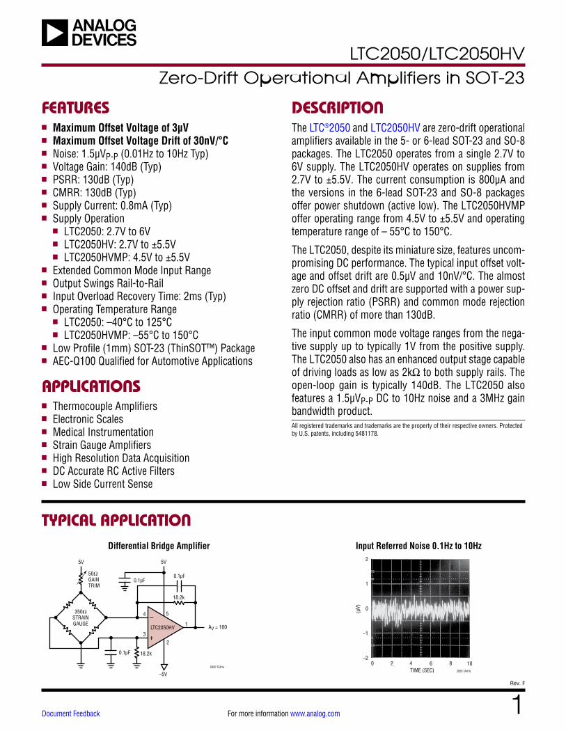
OUT 1
V– 2
TOP VIEW
S5 PACKAGE5-LEAD PLASTIC TSOT-23
TJMAX = 150°C, θJA = 250°C/W
+IN 3
5 V+
4 –IN
OUT 1
V– 2
+IN 3
6 V+
5 SHDN
4 –IN
TOP VIEW
S6 PACKAGE6-LEAD PLASTIC TSOT-23
TJMAX = 150°C, θJA = 230°C/W
1
2
3
4
8
7
6
5
TOP VIEW
NC
V+
OUT
NC
SHDN
–IN
+IN
V–
S8 PACKAGE8-LEAD PLASTIC SO
TJMAX = 150°C, θJA = 190°C/W
ABSOLUTE MAXIMUM RATINGS
Total Supply Voltage (V+ to V–) LTC2050 .................................................................7V LTC2050HV...........................................................12V
Input Voltage ........................(V+ + 0.3V) to (V– – 0.3V)Output Short-Circuit Duration ......................... Indefinite
(Note 1)
Operating Temperature Range LTC2050 ............................................ –40°C to 125°C LTC2050HVMP .................................. –55°C to 150°CSpecified Temperature Range (Note 3) .................................................. –55°C to 150°C Storage Temperature Range .................. –65°C to 150°CLead Temperature (Soldering, 10 sec) ................... 300°C
PIN CONFIGURATION
ORDER INFORMATIONLEAD FREE FINISH TAPE AND REEL PART MARKING* PACKAGE DESCRIPTION SPECIFIED TEMPERATURE RANGE
LTC2050CS5#PBF LTC2050CS5#TRPBF LTAEG 5-Lead Plastic TSOT-23 0°C to 70°C
LTC2050IS5#PBF LTC2050IS5#TRPBF LTAEG 5-Lead Plastic TSOT-23 –40°C to 85°C
LTC2050HS5#PBF LTC2050HS5#TRPBF LTAEG 5-Lead Plastic TSOT-23 –40°C to 125°C
LTC2050HVCS5#PBF LTC2050HVCS5#TRPBF LTAEH 5-Lead Plastic TSOT-23 0°C to 70°C
LTC2050HVIS5#PBF LTC2050HVIS5#TRPBF LTAEH 5-Lead Plastic TSOT-23 –40°C to 85°C
LTC2050HVHS5#PBF LTC2050HVHS5#TRPBF LTAEH 5-Lead Plastic TSOT-23 –40°C to 125°C
LTC2050CS6#PBF LTC2050CS6#TRPBF LTAEJ 6-Lead Plastic TSOT-23 0°C to 70°C
LTC2050IS6#PBF LTC2050IS6#TRPBF LTAEJ 6-Lead Plastic TSOT-23 –40°C to 85°C
LTC2050HS6#PBF LTC2050HS6#TRPBF LTAEJ 6-Lead Plastic TSOT-23 –40°C to 125°C
LTC2050HVMPS6#PBF LTC2050HVMPS6#TRPBF LTHGP 6-Lead Plastic TSOT-23 –55°C to 150°C
LTC2050HVCS6#PBF LTC2050HVCS6#TRPBF LTAEK 6-Lead Plastic TSOT-23 0°C to 70°C
LTC2050HVIS6#PBF LTC2050HVIS6#TRPBF LTAEK 6-Lead Plastic TSOT-23 –40°C to 85°C
LTC2050HVHS6#PBF LTC2050HVHS6#TRPBF LTAEK 6-Lead Plastic TSOT-23 –40°C to 125°C
LTC2050CS8#PBF LTC2050CS8#TRPBF 2050 8-Lead Plastic SO 0°C to 70°C
LTC2050IS8#PBF LTC2050IS8#TRPBF 2050I 8-Lead Plastic SO –40°C to 85°C
LTC2050HVCS8#PBF LTC2050HVCS8#TRPBF 2050HV 8-Lead Plastic SO 0°C to 70°C
LTC2050/LTC2050HV
3Rev. F
For more information www.analog.com
ORDER INFORMATIONLEAD FREE FINISH TAPE AND REEL PART MARKING* PACKAGE DESCRIPTION SPECIFIED TEMPERATURE RANGE
LTC2050HVIS8#PBF LTC2050HVIS8#TRPBF 050HVI 8-Lead Plastic SO –40°C to 85°C
AUTOMOTIVE PRODUCTS**
LTC2050HVMPS6#WPBF LTC2050HVMPS6#WTRPBF LTHGP 6-Lead Plastic TSOT-23 –55°C to 150°C
Contact the factory for parts specified with wider operating temperature ranges. *The temperature grade is identified by a label on the shipping container.
Tape and reel specifications. Some packages are available in 500 unit reels through designated sales channels with #TRMPBF suffix.**Versions of this part are available with controlled manufacturing to support the quality and reliability requirements of automotive applications. These
models are designated with a #W suffix. Only the automotive grade products shown are available for use in automotive applications. Contact your local Analog Devices account representative for specific product ordering information and to obtain the specific Automotive Reliability reports for these models.
ELECTRICAL CHARACTERISTICS
PARAMETER CONDITIONS
C, I SUFFIXES H SUFFIX
UNITSMIN TYP MAX MIN TYP MAXInput Offset Voltage (Note 2) ±0.5 ±3 ±0.5 ±3 µV
Average Input Offset Drift (Note 2) l ±0.03 ±0.05 µV/°C
Long-Term Offset Drift 50 50 nV/√mo
Input Bias Current LTC2050
l
±20 ±75 ±300
±20 ±75 ±4000
pA pA
LTC2050HV
l
±1 ±50 ±100
±1 ±50 ±4000
pA pA
Input Offset Current LTC2050
l
±150 ±200
±150 ±1000
pA pA
LTC2050HV
l
±100 ±150
±100 ±1000
pA pA
Input Noise Voltage RS = 100Ω, 0.01Hz to 10Hz 1.5 1.5 µVP-P
Input Capacitance 1.7 1.7 pF
Common Mode Rejection Ratio LTC2050/LTC2050HV VCM = GND to (V+ – 1.3) VCM = GND to (V+ – 1.3)
l
115 110
130 130
115 110
130 130
dB dB
Power Supply Rejection Ratio VS = 2.7V to 6V
l
120 115
130 130
120 115
130 130
dB dB
Large-Signal Voltage Gain RL = 10k
l
120 115
140 140
120 115
140 140
dB dB
Output Voltage Swing High RL = 2k to GND RL = 10k to GND
l
l
2.85 2.95
2.94 2.98
2.85 2.95
2.94 2.98
V V
Output Voltage Swing Low RL = 2k to GND RL = 10k to GND
l
l
1 1
10 10
1 1
10 10
mV mV
Slew Rate 2 2 V/µs
Gain Bandwidth Product 3 3 MHz
Supply Current VSHDN = VIH, No Load VSHDN = VIL
l
l
0.75 1.1 10
0.75 1.2 10
mA µA
Shutdown Pin Input Low Voltage (VIL) l V– + 0.5 V– + 0.5 V
Shutdown Pin Input High Voltage (VIH) l V+ – 0.5 V+ – 0.5 V
Shutdown Pin Input Current VSHDN = GND l –0.5 –3 –0.5 –3 µA
Internal Sampling Frequency 7.5 7.5 kHz
(LTC2050/LTC2050HV) The l denotes the specifications which apply over the full operating temperature range, otherwise specifications are at TA = 25°C. VS = 3V unless otherwise noted. (Note 3)

LTC2050/LTC2050HV
4Rev. F
For more information www.analog.com
PARAMETER CONDITIONS
C, I SUFFIXES H, MP SUFFIX
UNITSMIN TYP MAX MIN TYP MAX
Input Offset Voltage (Note 2) ±0.5 ±3 ±0.5 ±3 µV
Average Input Offset Drift (Note 2) LTC2050HVMP
l
l
±0.03 ±0.05 ±0.10
µV/°C µV/°C
Long-Term Offset Drift 50 50 nV/√mo
Input Bias Current LTC2050
l
±75 ±150 ±300
±75 ±150 ±4000
pA pA
LTC2050HV
l
±7 ±50 ±150
±7 ±50 ±4000
pA pA
LTC2050HVMP
l
±7 ±50 ±8000
pA pA
Input Offset Current LTC2050
l
±300 ±400
±300 ±1000
pA pA
LTC2050HV
l
±100 ±200
±100 ±1000
pA pA
LTC2050HVMP l ±2000 pA
Input Noise Voltage RS = 100Ω, 0.01Hz to 10Hz 1.5 1.5 µVP-P
Common Mode Rejection Ratio LTC2050/LTC2050HV VCM = GND to (V+ – 1.3) VCM = GND to (V+ – 1.3)
l
120 115
130 130
120 110
130 130
dB dB
LTC2050HVMP VCM = GND to (V+ – 1.3)
l
107
130
dB
Power Supply Rejection Ratio VS = 2.7V to 6V
l
120 115
130 130
120 115
130 130
dB dB
LTC2050HVMP VS = 4.5V to 11V
l
117 112
130 130
dB dB
Large-Signal Voltage Gain RL = 10k
l
125 120
140 140
125 115
140 140
dB dB
Output Voltage Swing High RL = 2k to GND RL = 10k to GND
l
l
4.85 4.95
4.94 4.98
4.85 4.95
4.94 4.98
V V
Output Voltage Swing Low RL = 2k to GND RL = 10k to GND
l
l
1 1
10 10
1 1
10 10
mV mV
Slew Rate 2 2 V/µs
Gain Bandwidth Product 3 3 MHz
Supply Current VSHDN = VIH, No Load VSHDN = VIL
l
l
0.8 1.2 15
0.8 1.3 15
mA µA
Shutdown Pin Input Low Voltage (VIL) l V– + 0.5 V– + 0.5 V
Shutdown Pin Input High Voltage (VIH) l V+ – 0.5 V+ – 0.5 V
Shutdown Pin Input Current VSHDN = GND l –0.5 –7 –0.5 –7 µA
Internal Sampling Frequency 7.5 7.5 kHz
ELECTRICAL CHARACTERISTICS The l denotes the specifications which apply over the full operating temperature range, otherwise specifications are at TA = 25°C. (LTC2050/LTC2050HV) VS = 5V unless otherwise noted. (Note 3)

LTC2050/LTC2050HV
5Rev. F
For more information www.analog.com
ELECTRICAL CHARACTERISTICS (LTC2050HV) The l denotes the specifications which apply over the full operating temperature range, otherwise specifications are at TA = 25°C. VS = ±5V unless otherwise noted. (Note 3)
PARAMETER CONDITIONS
C, I SUFFIXES H, MP SUFFIX
UNITSMIN TYP MAX MIN TYP MAX
Input Offset Voltage (Note 2) ±0.5 ±3 ±0.5 ±3 µV
Average Input Offset Drift (Note 2) LTC2050HVMP
l
l
±0.03 ±0.05 ±0.10
µV/°C µV/°C
Long-Term Offset Drift 50 50 nV/√mo
Input Bias Current (Note 4) LTC2050HV
l
±25 ±125 ±300
±25 ±125 ±4000
pA pA
LTC2050HVMP
l
±25 ±125 ±8000
pA pA
Input Offset Current (Note 4) LTC2050HV
l
±250 ±500
±250 ±1000
pA pA
LTC2050HVMP l ±2000 pA
Input Noise Voltage RS = 100Ω, 0.01Hz to 10Hz 1.5 1.5 µVP-P
Common Mode Rejection Ratio LTC2050HV VCM = V– to (V+ – 1.3) VCM = V– to (V+ – 1.3)
l
120 115
130 130
120 115
130 130
dB dB
LTC2050HVMP VCM = V– to (V+ – 1.3)
l
112
130
dB
Power Supply Rejection Ratio VS = 2.7V to 11V
l
120 115
130 130
120 115
130 130
dB dB
LTC2050HVMP VS = 4.5 to 11V
l
117 112
130 130
dB dB
Large-Signal Voltage Gain RL = 10k
l
125 120
140 140
125 120
140 140
dB dB
Maximum Output Voltage Swing RL = 2k to GND RL = 10k to GND
l
l
±4.75 ±4.90
±4.94 ±4.98
±4.50 ±4.85
±4.94 ±4.98
V V
Slew Rate 2 2 V/µs
Gain Bandwidth Product 3 3 MHz
Supply Current VSHDN = VIH, No Load VSHDN = VIL
l
l
1 1.5 25
1 1.6 25
mA µA
Shutdown Pin Input Low Voltage (VIL) l V– + 0.5 V– + 0.5 V
Shutdown Pin Input High Voltage (VIH) l V+ – 0.5 V+ – 0.5 V
Shutdown Pin Input Current VSHDN = V– l –3 –20 –3 –20 µA
Internal Sampling Frequency 7.5 7.5 kHz
Note 1: Stresses beyond those listed under Absolute Maximum Ratings may cause permanent damage to the device. Exposure to any Absolute Maximum Rating condition for extended periods may affect device reliability and lifetime.Note 2: These parameters are guaranteed by design. Thermocouple effects preclude measurements of these voltage levels during automated testing.Note 3: All versions of the LTC2050 are designed, characterized and expected to meet the extended temperature limits of –40°C and 125°C.
The LTC2050C/LTC2050HVC are guaranteed to meet the temperature limits of 0°C and 70°C. The LTC2050I/LTC2050HVI are guaranteed to meet the temperature limits of –40°C and 85°C. The LTC2050H/LTC2050HVH are guaranteed to meet the temperature limits of –40°C and 125°C. The LTC2050HVMP is guaranteed to meet the temperature limits of –55°C and 150°C.Note 4: The bias current measurement accuracy depends on the proximity of the supply bypass capacitor to the device under test, especially at ±5V supplies. Because of testing limitations on the placement of this bypass capacitor, the bias current at ±5V supplies is guaranteed by design to meet the data sheet limits, but tested to relaxed limits.

LTC2050/LTC2050HV
6Rev. F
For more information www.analog.com
TYPICAL PERFORMANCE CHARACTERISTICS
Common Mode Rejection Ratio vs Frequency
DC CMRR vs Common Mode Input Voltage
PSRR vs Frequency
Output Voltage Swing vs Load Resistance
Output Swing vs Output Current
Output Swing vs Load Resistance ±5V Supply
Output Swing vs Output Current ±5V Supply
Gain/Phase vs Frequency
Input Bias Current vs Temperature (LTC2050)
FREQUENCY (Hz)
20
CMRR
(dB)
40
80
120
140
1 100 1k 100k
2050 G01
010 10k
60
100
VS = 3V OR 5VVCM = 0.5VP-P
VCM (V)
20
CMRR
(dB)
40
80
120
140
1 3 40
2050 G02
02 5
60
100
VS = 3VVS = 5V
TA = 25°C
FREQUENCY (Hz)10
PSRR
(dB)
120
100
80
60
40
20
0100 1k 10k 100k
2050 G03
1M
–PSRR
+PSRR
OUTPUT CURRENT (mA)0.01
2
OUTP
UT V
OLTA
GE (V
)
3
4
5
0.1 1 10
2050 G05
1
0
6
VS = 5V
VS = 3V
FREQUENCY (Hz)
0
GAIN
(dB)
20
40
60
100
100 1k 100k 1M 10M
2050 G08
–20
–4010k
80
180
PHASE (DEG)160
140
120
100
200
80
GAIN
PHASE
VS = 3V OR 5VCL = 35pFRL = 10kΩ
TEMPERATURE (°C)–25
10
1
100
10k
1k
10075
2050 G09
–50 125
INPU
T BI
AS C
URRE
NT (p
A)
500 25
VS = 3V
VS = 5V
LOAD RESISTANCE (kΩ)0
OUTP
UT S
WIN
G (V
)
5
4
3
2
1
0
–1
–2
–3
–4
–58
2050 G06
2 4 6 10
RL TO GND
OUTPUT CURRENT (mA)0.01
OUTP
UT S
WIN
G (V
)
5
4
3
2
1
0
–1
–2
–3
–4
–5
2050 G07
0.1 101.0
RL TO GND
LOAD RESISTANCE (kΩ)0
OUTP
UT S
WIN
G (V
)
6
5
4
3
2
1
02 4
2050 G04
6 8 10
RL TO GND
VS = 5V
VS = 3V

LTC2050/LTC2050HV
7Rev. F
For more information www.analog.com
TYPICAL PERFORMANCE CHARACTERISTICS
Input Bias Current vs Input Common Mode Voltage
Input Bias Current vs Input Common Mode Voltage (LTC2050HV)
Transient Response
Input Overload Recovery
INPUT COMMON MODE VOLTAGE (V)0
INPU
T BI
AS C
URRE
NT M
AGNI
TUDE
(pA)
3 5
2050 G12
1 2 4
160
140
120
100
80
60
40
20
0
VS = 5V
VS = 3V
INPUT COMMON MODE VOLTAGE (V)
INPU
T BI
AS C
URRE
NT (p
A)60
50
40
30
20
10
0
–10
2050 G13
–5 –3 –1 1 3 5
VS = ±5V
VS = 5V
VS = 3V
1µs/DIV
0.5/DIV
2050 G14AV = 1RL = 100kCL = 50pFVS = 5V
500µs/DIV
INPUT (V)
OUTPUT (V)
–0.2
1.5
0
0
2050 G15AV = –100RL = 100kCL = 10pFVS = ±1.5V
Input Bias Current vs Temperature (LTC2050HVMP)
Input Bias Current vs Temperature (LTC2050HV)
VS = 5VVS = ±5V
TEMPERATURE (°C)–50 –25 0 25 50 75 100 125 150
1
10
100
1k
10k
INPU
T BI
AS C
URRE
NT (p
A)
2050 G10
VS = 3VVS = 5VVS = ±5V
TEMPERATURE (°C)–50 –15 20 55 90 125
1
10
100
1k
10k
INPU
T BI
AS C
URRE
NT (p
A)
2050 G11

LTC2050/LTC2050HV
8Rev. F
For more information www.analog.com
Sampling Frequency vs Supply Voltage
Sampling Frequency vs Temperature
Supply Current vs Supply Voltage
Supply Current vs Temperature
SUPPLY VOLTAGE (V)2.5
5
SAM
PLIN
G FR
EQUE
NCY
(kHz
)
6
7
3.53.0 4.54.0 5.0 5.5
2050 G16
8
9
10
6.0
TA = 25°C
VS = 5V
TEMPERATURE (°C)–50 –25 0 25 50 75 100 125 150
5
6
7
8
9
10
SAM
PLIN
G FR
EQUE
NCY
(kHz
)
2050 G17
SUPPLY VOLTAGE (V)
SUPP
LY C
URRE
NT (m
A)
2 4 6 8 10
1.2
1.0
0.8
0.6
0.4
0.2
0
2050 G18
TA = 25°C
VS = 3VVS = 5VVS = ±5V
TEMPERATURE (°C)–50 –30 –10 10 30 50 70 90 110 130 150
0.5
0.6
0.7
0.8
0.9
1.0
1.1SU
PPLY
CUR
RENT
(mA)
2050 G19
TYPICAL PERFORMANCE CHARACTERISTICS

LTC2050/LTC2050HV
9Rev. F
For more information www.analog.com
TEST CIRCUITS
Electrical Characteristics Test Circuit
DC−10Hz Noise Test Circuit
–
+LTC2050 –
+LT1012
10Ω
1
3
4
2050 TC02
100k 475k
475k316k158k
0.1µF 0.01µF
0.01µF
TO X-YRECORDER
FOR 1Hz NOISE BW INCREASE ALL THE CAPACITORS BY A FACTOR OF 10.
–
+LTC2050
V+
V–
10Ω
1
23
4 5
RL
2050 TC01
100kOUTPUT

LTC2050/LTC2050HV
10Rev. F
For more information www.analog.com
output multiplied by the closed loop gain of the op amp. To reduce this form of clock feedthrough, use smaller valued gain setting resistors and minimize the source resistance at the input. If the resistance seen at the inputs is less than 10k, this form of clock feedthrough is less than 1µVRMS input referred at 7.5kHz, or less than the amount of residue clock feedthrough from the first form described above.
Placing a capacitor across the feedback resistor reduces either form of clock feedthrough by limiting the bandwidth of the closed loop gain.
Input bias current is defined as the DC current into the input pins of the op amp. The same current spikes that cause the second form of clock feedthrough described above, when averaged, dominate the DC input bias current of the op amp below 70°C.
At temperatures above 70°C, the leakage of the ESD pro-tection diodes on the inputs increases the input bias cur-rents of both inputs in the positive direction, while the current caused by the charge injection stays relatively constant. At elevated temperatures (above 85°C) the leakage current begins to dominate and both the negative and positive pin’s input bias currents are in the positive direction (into the pins).
Input Pins, ESD Sensitivity
ESD voltages above 700V on the input pins of the op amp will cause the input bias currents to increase (more DC current into the pins). At these voltages, it is possible to damage the device to a point where the input bias current exceeds the maximums specified in this data sheet.
Shutdown
The LTC2050 includes a shutdown pin in the 6-lead SOT-23 and the SO-8 version. When this active low pin is high or allowed to float, the device operates normally. When the shutdown pin is pulled low, the device enters shutdown mode; supply current drops to 3µA, all clock-ing stops, and both inputs and output assume a high impedance state.
Clock Feedthrough, Input Bias Current
The LTC2050 uses auto-zeroing circuitry to achieve an almost zero DC offset over temperature, common mode voltage, and power supply voltage. The frequency of the clock used for auto-zeroing is typically 7.5kHz. The term clock feedthrough is broadly used to indicate visibility of this clock frequency in the op amp output spectrum. There are typically two types of clock feedthrough in auto zeroed op amps like the LTC2050.
The first form of clock feedthrough is caused by the settling of the internal sampling capacitor and is input referred; that is, it is multiplied by the closed loop gain of the op amp. This form of clock feedthrough is independent of the magnitude of the input source resistance or the magni-tude of the gain setting resistors. The LTC2050 has a resi-due clock feedthrough of less then 1µVRMS input referred at 7.5kHz.
The second form of clock feedthrough is caused by the small amount of charge injection occurring during the sampling and holding of the op amp’s input offset volt-age. The current spikes are multiplied by the impedance seen at the input terminals of the op amp, appearing at the
APPLICATIONS INFORMATION

LTC2050/LTC2050HV
11Rev. F
For more information www.analog.com
Single Supply Thermocouple Amplifier
Gain of 1001 Single Supply Instrumentation Amplifier
TYPICAL APPLICATIONS
2050 TA04
+
–
+
–
10k
10Ω
10Ω
10kV+
V+4 5
1
23
4 5
1
23
VOUT–VIN
+VIN
LTC2050
LTC2050
OUTPUT DC OFFSET ≤ 6mVFOR 0.1% RESISTORS, CMRR = 54dB
0.1µF
–
+– +
LT1025A
GND
K
R–
5V
0.1µF
LTC2050
5
1
4
54
3
2
2
TYPE K
7
VOUT10mV/°C
1k1%
255k1%100Ω
0.068µF
2050 TA03
LT1025 COMPENSATES COLD JUNCTION OVER 0°C TO 100°C TEMPERATURE RANGE
5V
Instrumentation Amplifier with 100V Common Mode Input Voltage
–
+LTC2050HV –
+LTC2050HV
1M
1M1
3
4
2050 TA06
1k 1M
1k
1k
VOUT
5
21
3
4 5
2
V+
V–
V+
V–
OUTPUT OFFSET ≤3mVFOR 0.1% RESISTORS, CMRR = 54dB
+
–
VIN
LTC2050/LTC2050HV
12Rev. F
For more information www.analog.com
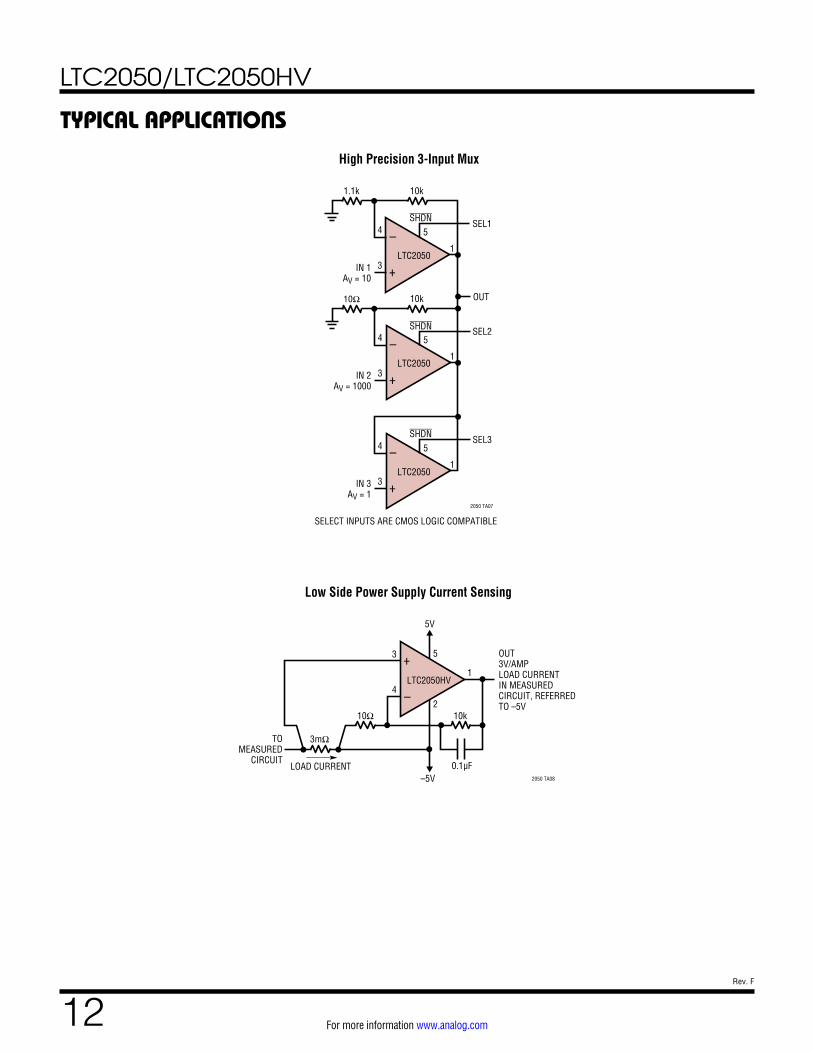
High Precision 3-Input Mux
–
+
1
3
4 5SEL1
10k1.1k
IN 1AV = 10
–
+
1
3
4 5SEL2
10k10Ω
IN 2AV = 1000
–
+
1
3
4 5SEL3
IN 3AV = 1
LTC2050
LTC2050
LTC2050
OUT
SELECT INPUTS ARE CMOS LOGIC COMPATIBLE
2050 TA07
SHDN
SHDN
SHDN
TYPICAL APPLICATIONS
Low Side Power Supply Current Sensing
–
+LTC2050HV
1
4
3
2050 TA08
5
2
5V
–5V
TOMEASURED
CIRCUIT
OUT 3V/AMPLOAD CURRENTIN MEASUREDCIRCUIT, REFERRED TO –5V
10Ω 10k
3mΩ
0.1µFLOAD CURRENT

LTC2050/LTC2050HV
13Rev. F
For more information www.analog.com
PACKAGE DESCRIPTION
1.50 – 1.75(NOTE 4)2.80 BSC
0.30 – 0.45 TYP 5 PLCS (NOTE 3)
DATUM ‘A’
0.09 – 0.20(NOTE 3) S5 TSOT-23 0302 REV B
PIN ONE
2.90 BSC(NOTE 4)
0.95 BSC
1.90 BSC
0.80 – 0.90
1.00 MAX0.01 – 0.100.20 BSC
0.30 – 0.50 REF
NOTE:1. DIMENSIONS ARE IN MILLIMETERS2. DRAWING NOT TO SCALE3. DIMENSIONS ARE INCLUSIVE OF PLATING4. DIMENSIONS ARE EXCLUSIVE OF MOLD FLASH AND METAL BURR5. MOLD FLASH SHALL NOT EXCEED 0.254mm6. JEDEC PACKAGE REFERENCE IS MO-193
3.85 MAX
0.62MAX
0.95REF
RECOMMENDED SOLDER PAD LAYOUTPER IPC CALCULATOR
1.4 MIN2.62 REF
1.22 REF
S5 Package5-Lead Plastic TSOT-23
(Reference LTC DWG # 05-08-1635 Rev B)
LTC2050/LTC2050HV
14Rev. F
For more information www.analog.com
PACKAGE DESCRIPTION
1.50 – 1.75(NOTE 4)
2.80 BSC
0.30 – 0.45 6 PLCS (NOTE 3)
DATUM ‘A’
0.09 – 0.20(NOTE 3) S6 TSOT-23 0302
2.90 BSC(NOTE 4)
0.95 BSC
1.90 BSC
0.80 – 0.90
1.00 MAX0.01 – 0.10
0.20 BSC
0.30 – 0.50 REF
PIN ONE ID
NOTE:1. DIMENSIONS ARE IN MILLIMETERS2. DRAWING NOT TO SCALE3. DIMENSIONS ARE INCLUSIVE OF PLATING4. DIMENSIONS ARE EXCLUSIVE OF MOLD FLASH AND METAL BURR5. MOLD FLASH SHALL NOT EXCEED 0.254mm6. JEDEC PACKAGE REFERENCE IS MO-193
3.85 MAX
0.62MAX
0.95REF
RECOMMENDED SOLDER PAD LAYOUTPER IPC CALCULATOR
1.4 MIN2.62 REF
1.22 REF
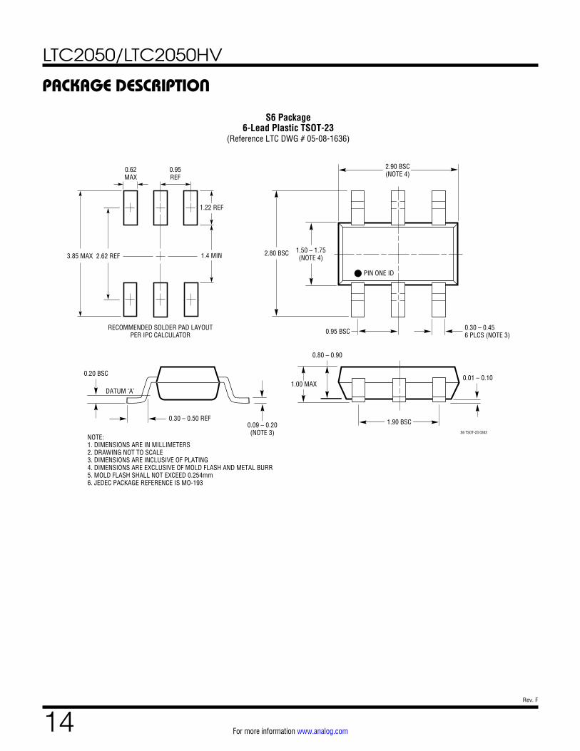
S6 Package6-Lead Plastic TSOT-23
(Reference LTC DWG # 05-08-1636)

LTC2050/LTC2050HV
15Rev. F
For more information www.analog.com
Information furnished by Analog Devices is believed to be accurate and reliable. However, no responsibility is assumed by Analog Devices for its use, nor for any infringements of patents or other rights of third parties that may result from its use. Specifications subject to change without notice. No license is granted by implication or otherwise under any patent or patent rights of Analog Devices.
PACKAGE DESCRIPTION
.016 – .050(0.406 – 1.270)
.010 – .020(0.254 – 0.508)
× 45°
0°– 8° TYP.008 – .010
(0.203 – 0.254)
SO8 REV G 0212
.053 – .069(1.346 – 1.752)
.014 – .019(0.355 – 0.483)
TYP
.004 – .010(0.101 – 0.254)
.050(1.270)
BSC
1 2 3 4
.150 – .157(3.810 – 3.988)
NOTE 3
8 7 6 5
.189 – .197(4.801 – 5.004)
NOTE 3
.228 – .244(5.791 – 6.197)
.245MIN .160 ±.005
RECOMMENDED SOLDER PAD LAYOUT
.045 ±.005 .050 BSC
.030 ±.005 TYP
INCHES(MILLIMETERS)
NOTE:1. DIMENSIONS IN
2. DRAWING NOT TO SCALE3. THESE DIMENSIONS DO NOT INCLUDE MOLD FLASH OR PROTRUSIONS. MOLD FLASH OR PROTRUSIONS SHALL NOT EXCEED .006" (0.15mm)4. PIN 1 CAN BE BEVEL EDGE OR A DIMPLE
S8 Package8-Lead Plastic Small Outline (Narrow .150 Inch)
(Reference LTC DWG # 05-08-1610 Rev G)
REVISION HISTORYREV DATE DESCRIPTION PAGE NUMBER
D 08/17 Updated TJMAX 2
E 11/18 Added MP option (higher temperature version) 1, 2, 4-6, 7-8
F 10/19 Added Automotive product option All
(Revision history begins at Rev D)

LTC2050/LTC2050HV
16Rev. F
For more information www.analog.com
10/19
ANALOG DEVICES, INC. 1999-2019www.analog.com
RELATED PARTS
TYPICAL APPLICATION
–
+LTC2050
LT1034
+
–VOUT
V+
10k
1
23
4 5
RSET
0 ≤ IOUT ≤ 4mA0.2V ≤ VOUT ≤ (V+) – 1.5V
–
+LTC2050
LT1034
+
–VOUT
V–
10k1
2
3
4
5 RSET
0 ≤ IOUT ≤ 4mA(V–) + 1.5V ≤ VOUT ≤ – 1V
2050 TA05
IOUT = ———RSET
1.235V
IOUT = ———RSET
1.235V
PART NUMBER DESCRIPTION COMMENTS
LTC1049 Low Power Zero-Drift Op Amp Low Supply Current 200µA
LTC1050 Precision Zero-Drift Op Amp Single Supply Operation 4.75V to 16V, Noise Tested and Guaranteed
LTC1051/LTC1053 Precision Zero-Drift Op Amp Dual/Quad
LTC1150 ±15V Zero-Drift Op Amp High Voltage Operation ±18V
LTC1152 Rail-to-Rail Input and Output Zero-Drift Op Amp Single Zero-Drift Op Amp with Rail-to-Rail Input and Output and Shutdown
LT®1677 Low Noise Rail-to-Rail Input and Output Precision Op Amp
VOS = 90µV, VS = 2.7V to 44V
LT1884/LT1885 Rail-to-Rail Output Precision Op Amp VOS = 50µV, IB = 400pA, VS = 2.7V to 40V
LTC2051 Dual Zero-Drift Op Amp Dual Version of the LTC2050 in MS8 Package
Ground Referred Precision Current Sources