Embed Size (px)
Citation preview

1
LTC17092-Phase, 5-Bit Adjustable,
High Efficiency, Synchronous Step-DownSwitching Regulator
, LTC and LT are registered trademarks of Linear Technology Corporation.OPTI-LOOP is a trademark of Linear Technology Corporation.
The LTC®1709 is a 2-phase, VID programmable, synchro-nous step-down switching regulator controller that drivesall N-channel external power MOSFET stages in a fixedfrequency architecture. The 2-phase controller drives itstwo output stages out of phase at frequencies up to300kHz to minimize the RMS ripple currents in both inputand output capacitors. The 2-phase technique effectivelymultiplies the fundamental frequency by two, improvingtransient response while operating each channel at aoptimum frequency for efficiency. Thermal design is alsosimplified.
An internal differential amplifier provides true remotesensing of the regulated supply’s positive and negativeoutput terminals as required in high current applications.
The RUN/SS pin provides soft-start and optional timed,short-circuit shutdown. Current foldback limits MOSFETdissipaton during short-circuit conditions when overcurrentlatchoff is disabled. OPTI-LOOP compensation allows thetransient response to be optimized for a wide range ofoutput capacitors and ESR values.
Figure 1. High Current 2-Phase Step-Down Converter
Desktop Computers Internet/Network Servers Large Memory Arrays DC Power Distribution Systems Battery Chargers
Two Ouput Stages Operate Antiphase ReducingInput Capacitance and Power Supply Noise
5-Bit VID Control (VRM 8.4 Compliant)VOUT: 1.3V to 3.5V in 50mV/100mV Steps
Current Mode Control Ensures Current Sharing True Remote Sensing Differential Amplifier OPTI-LOOPTM Compensation Minimizes COUT Programmable Fixed Frequency: 150kHz to
300kHz—Effective 300kHz to 600kHz SwitchingFrequency
±1% Output Voltage Accuracy Wide VIN Range: 4V to 36V Operation Adjustable Soft-Start Current Ramping Internal Current Foldback Short-Circuit Shutdown Timer with Defeat Option Overvoltage Soft-Latch Eliminates Nuisance Trips Low Shutdown Current: 20µA Small 36-Lead Narrow (0.209") SSOP Package
1709 TA01
TG1BOOST 1
SW1BG1
PGND
SENSE1+
SENSE1–
TG2BOOST2
SW2BG2
INTVCCSENSE 2+
SENSE 2–
VINRUN/SS
VDIFFOUT
ITH
SENSEINFBOUTEAIN
VID0–VID4
VOS–
VOS+
LTC1709
SGND
0.1µF
1.2nF
5 VID BITS
S
S
S
S
S
S
15k
+
10µF ×435V
+ COUT1000µF4V×2
VOUT1.3V TO 3.5V40A
1µH
Q1
Q2
Q3
Q4
0.002Ω
0.002Ω
VIN5V TO 28V
1µH
0.47µF
S
0.47µF
10µF
Q1–Q4 2× FAIRCHILD FDS7760A OR SILICONIX Si4874
APPLICATIO SU
FEATURES
TYPICAL APPLICATIO
U
DESCRIPTIO
U
Efficiency Curve
LOAD CURRENTS (A)0
50
EFFI
CIEN
CY (%
)
60
80
90
100
10 20 25 45
1709 TA01a
70
5 15 30 35 40
VIN = 5VVOUT = 1.6VfS = 200kHz

2
LTC1709
ORDER PARTNUMBER
LTC1709EG
ABSOLUTE AXI U RATI GS
W WW U
PACKAGE/ORDER I FOR ATIOU UW
TJMAX = 125°C, θJA = 85°C/W
Consult factory for Industrial and Military grade parts.
ELECTRICAL CHARACTERISTICS The denotes the specifications which apply over the full operatingtemperature range, otherwise specifications are at TA = 25°C. VIN = 15V, VRUN/SS = 5V unless otherwise noted.
(Note 1)
Input Supply Voltage (VIN) .........................36V to –0.3VTopside Driver Voltages (BOOST 1, 2) .......42V to –0.3VSwitch Voltage (SW1, 2) .............................36V to –5 VSENSE 1+, SENSE 2 +, SENSE 1–,SENSE 2– Voltages ....................... (1.1)INTVCC to –0.3VEAIN, VOS
+, VOS–, EXTVCC, INTVCC, RUN/SS,
AMPMD, VBIAS, ATTENIN, ATTENOUT,VID0–VID4, Voltages ...................................7V to –0.3VBoosted Driver Voltage (BOOST-SW) ..........7V to –0.3VPLLFLTR, PLLIN, VDIFFOUT Voltages .... INTVCC to –0.3VITH Voltage ................................................2.7V to –0.3VPeak Output Current <1µs(TGL1, 2; BG1, 2) .............. 3AINTVCC RMS Output Current ................................ 50mAOperating Ambient Temperature Range(Note 2) .................................................. –40°C to 85°CJunction Temperature (Note 3) ............................. 125°CStorage Temperature Range ................. –65°C to 150°CLead Temperature (Soldering, 10 sec).................. 300°C
SYMBOL PARAMETER CONDITIONS MIN TYP MAX UNITS
Main Control Loop
VEAIN Regulated Feedback Voltage (Note 4); ITH Voltage = 1.2V 0.792 0.800 0.808 V
VSENSEMAX Maximum Current Sense Threshold VSENSE– = 5V 62 75 88 mV
IINEAIN Feedback Current (Note 4) –5 – 50 nA
VLOADREG Output Voltage Load Regulation (Note 4)Measured in Servo Loop; ∆ITH Voltage: 1.2V to 0.7V 0.1 0.5 %Measured in Servo Loop; ∆ITH Voltage: 1.2V to 2V – 0.1 – 0.5 %
VREFLNREG Reference Voltage Line Regulation VIN = 3.6V to 30V (Note 4) 0.002 0.02 %/V
VOVL Output Overvoltage Threshold Measured at VEAIN 0.84 0.86 0.88 V
UVLO Undervoltage Lockout VIN Ramping Down 3 3.5 4 V
gm Transconductance Amplifier gm ITH = 1.2V; Sink/Source 5µA; (Note 4) 3 mmho
gmOL Transconductance Amplifier Gain ITH = 1.2V; (gmxZL; No Ext Load); (Note 4) 1.5 V/mV
IQ Input DC Supply Current (Note 5)Normal Mode EXTVCC Tied to VOUT; VOUT = 5V 470 µAShutdown VRUN/SS = 0V 20 40 µA
IRUN/SS Soft-Start Charge Current VRUN/SS = 1.9V – 0.5 –1.2 µA
VRUN/SS RUN/SS Pin ON Arming VRUN/SS Rising 1.0 1.5 1.9 V
1
2
3
4
5
6
7
8
9
10
11
12
13
14
15
16
17
18
TOP VIEW
G PACKAGE36-LEAD PLASTIC SSOP
36
35
34
33
32
31
30
29
28
27
26
25
24
23
22
21
20
19
RUNN/SS
SENSE 1+
SENSE 1–
EAIN
PLLFLTR
PLLIN
NC
ITH
SGND
VDIFFOUT
VOS–
VOS+
SENSE 2–
SENSE 2+
ATTENOUT
ATTENIN
VID0
VID1
NC
TG1
SW1
BOOST 1
VIN
BG1
EXTVCC
INTVCC
PGND
BG2
BOOST 2
SW2
TG2
AMPMD
VBIAS
VID4
VID3
VID2

3
LTC1709
SYMBOL PARAMETER CONDITIONS MIN TYP MAX UNITS
ELECTRICAL CHARACTERISTICS The denotes the specifications which apply over the full operatingtemperature range, otherwise specifications are at TA = 25°C. VIN = 15V, VRUN/SS = 5V unless otherwise noted.
VRUN/SSLO RUN/SS Pin Latchoff Arming VRUN/SS Rising from 3V 4.1 4.5 V
ISCL RUN/SS Discharge Current Soft Short Condition VEAIN = 0.5V; 0.5 2 4 µAVRUN/SS = 4.5V
ISDLHO Shutdown Latch Disable Current VEAIN = 0.5V 1.6 5 µA
ISENSE Total Sense Pins Source Current Each Channel: VSENSE1–, 2– = VSENSE1+, 2+ = 0V – 85 – 60 µA
DFMAX Maximum Duty Factor In Dropout 98 99.5 %
Top Gate Transition Time: (Note 6)TG1, 2 tr Rise Time CLOAD = 3300pF 30 90 nsTG1, 2 tf Fall Time CLOAD = 3300pF 40 90 ns
Bottom Gate Transition Time: (Note 6)BG1, 2 tr Rise Time CLOAD = 3300pF 30 90 nsBG1, 2 tf Fall Time CLOAD = 3300pF 20 90 ns
TG/BG t1D Top Gate Off to Bottom Gate On Delay (Note 6)Synchronous Switch-On Delay Time CLOAD = 3300pF Each Driver 90 ns
BG/TG t2D Bottom Gate Off to Top Gate On Delay (Note 6)Top Switch-On Delay Time CLOAD = 3300pF Each Driver 90 ns
tON(MIN) Minimum On-Time Tested with a Square Wave (Note 7) 180 200 ns
Internal VCC Regulator
VINTVCC Internal VCC Voltage 6V < VIN < 30V; VEXTVCC = 4V 4.8 5.0 5.2 V
VLDO INT INTVCC Load Regulation ICC = 0 to 20mA; VEXTVCC = 4V 0.2 1.0 %
VLDO EXT EXTVCC Voltage Drop ICC = 20mA; VEXTVCC = 5V 120 240 mV
VEXTVCC EXTVCC Switchover Voltage ICC = 20mA, EXTVCC Ramping Positive 4.5 4.7 V
VLDOHYS EXTVCC Switchover Hysteresis ICC = 20mA, EXTVCC Ramping Negative 0.2 V
VID Parameters
RATTEN Resistance Between ATTENIN and 20 kΩATTENOUT Pins
ATTENERR Resistive Divider Worst-Case Error Programmed from 1.3V to 2.05V (VID4 = 0) –0.25 +0.25 %Programmed from 2.1V to 3.5V (VID4 = 1) –0.35 +0.25 %
RPULLUP VID0–VID4 Pull-Up Resistance (Note 8) 40 kΩVIDTHLOW VID0–VID4 Logic Threshold Low 0.4 V
VIDTHHIGH VID0–VID4 Logic Threshold High 1.6 V
VIDLEAK VID0–VID4 Leakage VBIAS < VID0–VID4 < 7V 1 µA
Oscillator and Phase-Locked Loop
fNOM Nominal Frequency VPLLFLTR = 1.2V 190 220 250 kHz
fLOW Lowest Frequency VPLLFLTR = 0V 120 140 160 kHz
fHIGH Highest Frequency VPLLFLTR ≥ 2.4V 280 310 360 kHz
RPLLIN PLLIN Input Resistance 50 kΩIPLLFLTR Phase Detector Output Current
Sinking Capability fPLLIN < fOSC – 15 µASourcing Capability fPLLIN > fOSC 15 µA
RRELPHS Controller 2-Controller 1 Phase 180 Deg
Differential Amplifier/Op Amp Gain Block (Note 9)
ADA Gain Differential Amp Mode 0.995 1 1.005 V/V
CMRRDA Common Mode Rejection Ratio Differential Amp Mode; 0V < VCM < 5V 46 55 dB

4
LTC1709
ELECTRICAL CHARACTERISTICS The denotes the specifications which apply over the full operatingtemperature range, otherwise specifications are at TA = 25°C. VIN = 15V, VRUN/SS = 5V unless otherwise noted.
Note 6: Rise and fall times are measured using 10% and 90% levels. Delaytimes are measured using 50% levels.Note 7: The minimum on-time condition corresponds to the on inductorpeak-to-peak ripple current ≥40% IMAX (see Minimum On-TimeConsiderations in the Applications Information section).Note 8: Each built-in pull-up resistor attached to the VID inputs also has aseries diode to allow input voltages higher than the VIDVCC supply withoutdamage or clamping (see the Applications Information section).Note 9: When the AMPMD pin is high, the IC pins are connected directly tothe internal op amp inputs. When the AMPMD pin is low, internal MOSFETswitches connect four 40k resistors around the op amp to create astandard unity-gain differential amp.
Note 1: Absolute Maximum Ratings are those values beyond which thelife of a device may be impaired.Note 2: The LTC1709EG is guaranteed to meet performance specificationsfrom 0°C to 70°C. Specifications over the –40°C to 85°C operatingtemperature range are assured by design, characterization and correlationwith statistical process controls.Note 3: TJ is calculated from the ambient temperature TA and powerdissipation PD according to the following formulas:LTC1709EG: TJ = TA + (PD • 85°C/W)Note 4: The LTC1709 is tested in a feedback loop that servos VITH to aspecified voltage and measures the resultant VEAIN.Note 5: Dynamic supply current is higher due to the gate charge beingdelivered at the switching frequency. See Applications Information.
SYMBOL PARAMETER CONDITIONS MIN TYP MAX UNITS
RIN Input Resistance Differential Amp Mode; Measured at VOS+ Input 80 kΩVOS Input Offset Voltage Op Amp Mode; VCM = 2.5V; VDIFFOUT = 5V; 6 mV
IDIFFOUT = 1mA
IB Input Bias Current Op Amp Mode 30 200 nA
AOL Open Loop DC Gain Op Amp Mode; 0.7V ≤ VDIFFOUT < 10V 5000 V/mV
VCM Common Mode Input Voltage Range Op Amp Mode 0 3 V
CMRROA Common Mode Rejection Ratio Op Amp Mode; 0V < VCM < 3V 70 90 dB
PSRROA Power Supply Rejection Ratio Op Amp Mode; 6V < VIN < 30V 70 90 dB
ICL Maximum Output Current Op Amp Mode; VDIFFOUT = 0V 10 35 mA
VO(MAX) Maximum Output Voltage Op Amp Mode; IDIFFOUT = 1mA 10 11 V
GBW Gain-Bandwidth Product Op Amp Mode; IDIFFOUT = 1mA 2 MHz
SR Slew Rate Op Amp Mode; RL = 2k 5 V/µs
TYPICAL PERFOR A CE CHARACTERISTICS
UW
Efficiency vs Output Current(Figure 12)
Efficiency vs Output Current(Figure 12)
Efficiency vs Input Voltage(Figure 12)
OUTPUT CURRENT (A)
EFFI
CIEN
CY (%
)
100
80
60
40
20
0
1709 G01
0.1 1 10 100
VOUT = 2VVEXTVCC = 0Vf = 200kHz
VIN = 5V
VIN = 8V
VIN = 12V
VIN = 20V
OUTPUT CURRENT (A)
EFFI
CIEN
CY (%
)
1709 G02
100
80
60
40
20
00.1 1 10 100
VOUT = 2VVIN = 12Vf = 200kHz
INTERNAL LDO VS EXTERNALLYAPPLIED 5V OVERALL EFFICIENCY(FIGURE 12)
VEXTVCC = 5VVEXTVCC = 0V
VIN (V)5
EFFI
CIEN
CY (%
)
100
90
80
70
1709 G03
10 15 20
VOUT = 3.3VVEXTVCC = 5VIOUT = 20A

5
LTC1709
Internal 5V LDO Line RegMaximum Current Sense Thresholdvs Duty Factor
Maximum Current Sense Thresholdvs Percent of Nominal OutputVoltage (Foldback)
Maximum Current Sense Thresholdvs VRUN/SS (Soft-Start)
Maximum Current Sense Thresholdvs Sense Common Mode Voltage
Current Sense Thresholdvs ITH Voltage
INTVCC and EXTVCC SwitchVoltage vs Temperature
Supply Current vs Input Voltageand Mode EXTVCC Voltage Drop
TYPICAL PERFOR A CE CHARACTERISTICS
UW
INPUT VOLTAGE (V)0 5
0
SUPP
LY C
URRE
NT (µ
A)
400
1000
10 20 25
1709 G04
200
800
600
15 30 35
ON
SHUTDOWN
CURRENT (mA)0
EXTV
CC V
OLTA
GE D
ROP
(mV)
150
200
250
40
1709 G05
100
50
010 20 30 50
TEMPERATURE (°C)–50
INTV
CC A
ND E
XTV C
C SW
ITCH
VOL
TAGE
(V)
4.95
5.00
5.05
25 75
1709 G06
4.90
4.85
–25 0 50 100 125
4.80
4.70
4.75
INTVCC VOLTAGE
EXTVCC SWITCHOVER THRESHOLD
INPUT VOLTAGE (V)0
4.8
4.9
5.1
15 25
1709 G07
4.7
4.6
5 10 20 30 35
4.5
4.4
5.0
INTV
CC V
OLTA
GE (V
)
ILOAD = 1mA
DUTY FACTOR (%)0
0
V SEN
SE (m
V)
25
50
75
20 40 60 80
1709 G08
100
PERCENT ON NOMINAL OUTPUT VOLTAGE (%)0
V SEN
SE (m
V)
40
50
60
100
1709 G09
30
20
025 50 75
10
80
70
VRUN/SS (V)0
0
V SEN
SE (m
V)
20
40
60
80
1 2 3 4
1709 G10
5 6
VSENSE(CM) = 1.6V
COMMON MODE VOLTAGE (V)0
V SEN
SE (m
V) 72
76
80
4
1709 G11
68
64
601 2 3 5
VITH (V)0
V SEN
SE (m
V)
30
50
70
90
2
1709 G12
10
–10
20
40
60
80
0
–20
–300.5 1 1.5 2.5

6
LTC1709
Load Regulation VITH vs VRUN/SS SENSE Pins Total Source Current
Current Sense Pin Input Currentvs Temperature
EXTVCC Switch Resistancevs Temperature
Maximum Current SenseThreshold vs Temperature Soft-Start Up (Figure 12)
VITH1V/DIV
VOUT2V/DIV
VRUNSS2V/DIV
100ms/DIV 1629 G19
RUN/SS Current vs Temperature
TYPICAL PERFOR A CE CHARACTERISTICS
UW
LOAD CURRENT (A)0
NORM
ALIZ
ED V
OUT
(%)
–0.2
–0.1
4
1709 G13
–0.3
–0.41 2 3 5
0.0FCB = 0VVIN = 15VFIGURE 1
VRUN/SS (V)0
0
V ITH
(V)
0.5
1.0
1.5
2.0
2.5
1 2 3 4
1709 G14
5 6
VOSENSE = 0.7V
VSENSE COMMON MODE VOLTAGE (V)0
I SEN
SE (µ
A)
0
1709 G15
–50
–1002 4
50
100
6
TEMPERATURE (°C)–50 –25
70
V SEN
SE (m
V)
74
80
0 50 75
1709 G17
72
78
76
25 100 125TEMPERATURE (°C)
–50 –250
RUN/
SS C
URRE
NT (µ
A)
0.2
0.6
0.8
1.0
75 10050
1.8
1709 G18
0.4
0 25 125
1.2
1.4
1.6
TEMPERATURE (°C)–50 –25
0
EXTV
CC S
WIT
CH R
ESIS
TANC
E (Ω
)
4
10
0 50 75
1709 G22
2
8
6
25 100 125TEMPERATURE (°C)
–50 –2525
CURR
ENT
SENS
E IN
PUT
CURR
ENT
(µA)
29
35
0 50 75
1709 G21
27
33
31
25 100 125
EXTVCC = 5V
IOUT10A/DIV
VOUT50mV/DIV
20µs/DIV 1709 G20
0A
20A
Load Step Response Using ActiveVoltage Positioning (Figure 12)
7
LTC1709
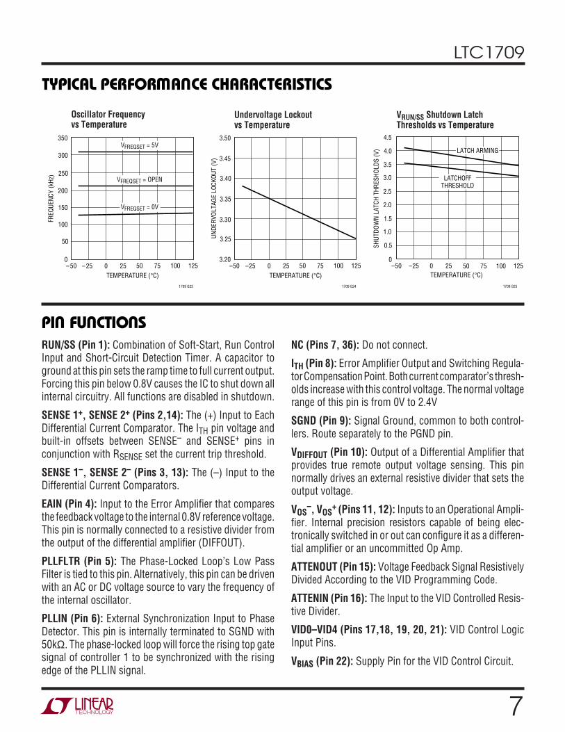
Oscillator Frequencyvs Temperature
Undervoltage Lockoutvs Temperature
VRUN/SS Shutdown LatchThresholds vs Temperature
TYPICAL PERFOR A CE CHARACTERISTICS
UW
TEMPERATURE (°C)–50 –25
0
SHUT
DOW
N LA
TCH
THRE
SHOL
DS (V
)
0.5
1.5
2.0
2.5
75 10050
4.5
1709 G25
1.0
0 25 125
3.0
3.5
4.0 LATCH ARMING
LATCHOFFTHRESHOLD
TEMPERATURE (°C)–50
UNDE
RVOL
TAGE
LOC
KOUT
(V)
3.40
3.45
3.50
25 75
1709 G24
3.35
3.30
–25 0 50 100 125
3.25
3.20
TEMPERATURE (°C)–50
200
250
350
25 75
1709 G23
150
100
–25 0 50 100 125
50
0
300
FREQ
UENC
Y (k
Hz)
VFREQSET = 5V
VFREQSET = OPEN
VFREQSET = 0V
RUN/SS (Pin 1): Combination of Soft-Start, Run ControlInput and Short-Circuit Detection Timer. A capacitor toground at this pin sets the ramp time to full current output.Forcing this pin below 0.8V causes the IC to shut down allinternal circuitry. All functions are disabled in shutdown.
SENSE 1+, SENSE 2+ (Pins 2,14): The (+) Input to EachDifferential Current Comparator. The ITH pin voltage andbuilt-in offsets between SENSE– and SENSE+ pins inconjunction with RSENSE set the current trip threshold.
SENSE 1–, SENSE 2– (Pins 3, 13): The (–) Input to theDifferential Current Comparators.
EAIN (Pin 4): Input to the Error Amplifier that comparesthe feedback voltage to the internal 0.8V reference voltage.This pin is normally connected to a resistive divider fromthe output of the differential amplifier (DIFFOUT).
PLLFLTR (Pin 5): The Phase-Locked Loop’s Low PassFilter is tied to this pin. Alternatively, this pin can be drivenwith an AC or DC voltage source to vary the frequency ofthe internal oscillator.
PLLIN (Pin 6): External Synchronization Input to PhaseDetector. This pin is internally terminated to SGND with50kΩ. The phase-locked loop will force the rising top gatesignal of controller 1 to be synchronized with the risingedge of the PLLIN signal.
NC (Pins 7, 36): Do not connect.
ITH (Pin 8): Error Amplifier Output and Switching Regula-tor Compensation Point. Both current comparator’s thresh-olds increase with this control voltage. The normal voltagerange of this pin is from 0V to 2.4V
SGND (Pin 9): Signal Ground, common to both control-lers. Route separately to the PGND pin.
VDIFFOUT (Pin 10): Output of a Differential Amplifier thatprovides true remote output voltage sensing. This pinnormally drives an external resistive divider that sets theoutput voltage.
VOS–, VOS
+ (Pins 11, 12): Inputs to an Operational Ampli-fier. Internal precision resistors capable of being elec-tronically switched in or out can configure it as a differen-tial amplifier or an uncommitted Op Amp.
ATTENOUT (Pin 15): Voltage Feedback Signal ResistivelyDivided According to the VID Programming Code.
ATTENIN (Pin 16): The Input to the VID Controlled Resis-tive Divider.
VID0–VID4 (Pins 17,18, 19, 20, 21): VID Control LogicInput Pins.
VBIAS (Pin 22): Supply Pin for the VID Control Circuit.
PI FU CTIO S
UUU

8
LTC1709
PI FU CTIO S
UUU
AMPMD (Pin 23): This Logic Input pin controls theconnections of internal precision resistors that configurethe operational amplifier as a unity-gain differentialamplifier.
TG2, TG1 (Pins 24, 35): High Current Gate Drives for TopN-Channel MOSFETS. These are the outputs of floatingdrivers with a voltage swing equal to INTVCC superim-posed on the switch node voltage SW.
SW2, SW1 (Pins 25, 34): Switch Node Connections toInductors. Voltage swing at these pins is from a Schottkydiode (external) voltage drop below ground to VIN.
BOOST 2, BOOST 1 (Pins 26, 33): Bootstrapped Suppliesto the Topside Floating Drivers. External capacitors areconnected between the Boost and Switch pins, and Schottkydiodes are connected between the Boost and INTVCC pins.
BG2, BG1 (Pins 27, 31): High Current Gate Drives forBottom N-Channel MOSFETS. Voltage swing at these pinsis from ground to INTVCC.
PGND (Pin 28): Driver Power Ground, connect to sourcesof bottom N-channel MOSFETS and the (–) terminals ofCIN.
INTVCC (Pin 29): Output of the Internal 5V Linear LowDropout Regulator and the EXTVCC Switch. The driver andcontrol circuits are powered from this voltage source.Decouple to power ground with a 1µF ceramic capacitorplaced directly adjacent to the IC and minimum of 4.7µFadditional tantalum or other low ESR capacitor.
EXTVCC (Pin 30): External Power Input to an InternalSwitch . This switch closes and supplies INTVCC, bypass-ing the internal low dropout regulator whenever EXTVCC ishigher than 4.7V. See EXTVCC Connection in the Applica-tions Information section. Do not exceed 7V on this pinand ensure VEXTVCC ≤ VIN.
VIN (Pin 32): Main Supply Pin. Should be closely decoupledto the IC’s signal ground pin.

9
LTC1709
FU CTIO AL DIAGRA
UU W
SWITCHLOGIC
0.8V
4.7V
5V
VIN
VIN
A1
CLK2
TOSECONDCHANNEL
CLK1
+
–
+
–
–
+
VREF
INTERNALSUPPLY
EXTVCC
INTVCC
SGND
+
5VLDOREG
SW
SHDN
TOP
BOOST
TG CB
CIN
DB
PGND*
BOTBG
INTVCC
INTVCC
VIN
+
VOUT
1709 FBD
EAIN
DROPOUTDET
RUNSOFT-START
BOT
FORCE BOTS
R
Q
Q
OSCILLATOR
PLLFLTR
50k
EA
0.86V
0.80VOV
VFB
1.2µA
6V
VIN –
+
RC
4(VFB)
SHDNRST
RUN/SS
TYPICAL ALLVID PINS
ITHCC
CSS
4(VFB)
SLOPECOMP
+
–
SENSE–
SENSE+
INTVCC
30k
45k
2.4V
45k
30k
I1
VID0 VID1 VID2 VID4
40k
VBIAS
ATTENIN
ATTENOUT
R220k
R1 R1 VARIABLE
AMPMD
DIFFOUT0V POSITION
PHASE DETPLLIN
DUPLICATE FOR SECOND CHANNEL
+–
RSENSE
L
COUT
+
VOS+
VOS–
FIN
RLP
CLP
VID3
5-BIT VID DECODER

10
LTC1709
OPERATIOU
(Refer to Functional Diagram)
Main Control Loop
The LTC1709 uses a constant frequency, current modestep-down architecture with inherent current sharing.During normal operation, the top MOSFET is turned oneach cycle when the oscillator sets the RS latch, andturned off when the main current comparator, I1, resetsthe RS latch. The peak inductor current at which I1 resetsthe RS latch is controlled by the voltage on the ITH pin,which is the output of the error amplifier EA. The differen-tial amplifier, A1, produces a signal equal to the differentialvoltage sensed across the output capacitor but re-refer-ences it to the internal signal ground (SGND) reference.The EAIN pin receives a portion of this voltage feedbacksignal at the DIFFOUT as determined by VID logic inputpins (VID0 to VID4) and is compared to the internalreference voltage by the EA. When the load current in-creases, it causes a slight decrease in the EAIN pin voltagerelative to the 0.8V reference, which in turn causes the ITHvoltage to increase until the average inductor currentmatches the new load current. After the top MOSFET hasturned off, the bottom MOSFET is turned on for the rest ofthe period.
The top MOSFET drivers are biased from floating boot-strap capacitor CB, which normally is recharged duringeach off cycle through an external Schottky diode. WhenVIN decreases to a voltage close to VOUT, however, the loopmay enter dropout and attempt to turn on the top MOSFETcontinuously. A dropout detector detects this conditionand forces the top MOSFET to turn off for about 400nsevery 10th cycle to recharge the bootstrap capacitor, CB.
The main control loop is shut down by pulling Pin 1 (RUN/SS) low. Releasing RUN/SS allows an internal 1.2µAcurrent source to charge soft-start capacitor CSS. WhenCSS reaches 1.5V, the main control loop is enabled with theITH voltage clamped at approximately 30% of its maximumvalue. As CSS continues to charge, ITH is gradually re-leased allowing normal operation to resume. When theRUN/SS pin is low, all LTC1709 functions are shut down.If VOUT has not reached 70% of its nominal value when CSShas charged to 4.1V, an overcurrent latchoff can beinvoked as described in the Applications Informationsection.
Low Current Operation
The LTC1709 operates in a continuous, PWM controlmode. The resulting operation at low output currentsoptimizes transient response at the expense of substantialnegative inductor current during the latter part of theperiod. The level of ripple current is determined by theinductor value, input voltage, output voltage, and fre-quency of operation.
Frequency Synchronization
The phase-locked loop allows the internal oscillator to besynchronized to an external source via the PLLIN pin. Theoutput of the phase detector at the PLLFLTR pin is also theDC frequency control input of the oscillator that operatesover a 140kHz to 310kHz range corresponding to a DCvoltage input from 0V to 2.4V. When locked, the PLL alignsthe turn on of the top MOSFET to the rising edge of thesynchronizing signal. When PLLIN is left open, the PLLFLTRpin goes low, forcing the oscillator to minimum frequency.
Input capacitance ESR requirements and efficiency lossesare substantially reduced because the peak current drawnfrom the input capacitor is effectively divided by two andpower loss is proportional to the RMS current squared. Atwo stage, single output voltage implementation can re-duce input path power loss by 75% and radically reducethe required RMS current rating of the input capacitor(s).
INTVCC/EXTVCC Power
Power for the top and bottom MOSFET drivers and mostof the IC circuitry is derived from INTVCC. When theEXTVCC pin is left open, an internal 5V low dropoutregulator supplies INTVCC power. If the EXTVCC pin istaken above 4.7V, the 5V regulator is turned off and aninternal switch is turned on connecting EXTVCC to INTVCC.This allows the INTVCC power to be derived from a highefficiency external source such as the output of the regu-lator itself or a secondary winding, as described in theApplications Information section. An external Schottkydiode can be used to minimize the voltage drop fromEXTVCC to INTVCC in applications requiring greater thanthe specified INTVCC current. Voltages up to 7V can beapplied to EXTVCC for additional gate drive capability.

11
LTC1709
OPERATIOU
(Refer to Functional Diagram)
Differential Amplifier
This amplifier provides true differential output voltagesensing. Sensing both VOUT
+ and VOUT– benefits regula-
tion in high current applications and/or applications hav-ing electrical interconnection losses. The AMPMD pinallows selection of internal, precision feedback resistorsfor high common mode rejection differencing applica-tions, or direct access to the actual amplifier inputswithout these internal feedback resistors for other applica-tions. The AMPMD pin is grounded to connect the internalprecision resistors in a unity-gain differencing application,or tied to the INTVCC pin to bypass the internal resistorsand make the amplifier inputs directly available. Theamplifier is a unity-gain stable, 2MHz gain-bandwidth,>120dB open-loop gain design. The amplifier has anoutput slew rate of 5V/µs and is capable of driving capaci-tive loads with an output RMS current typically up to35mA. The amplifier is not capable of sinking current andtherefore must be resistively loaded to do so.
Short-Circuit Detection
The RUN/SS capacitor is used initially to limit the inrushcurrent from the input power source. Once the controllershave been given time, as determined by the capacitor onthe RUN/SS pin, to charge up the output capacitors andprovide full-load current, the RUN/SS capacitor is thenused as a short-circuit timeout circuit. If the output voltagefalls to less than 70% of its nominal output voltage theRUN/SS capacitor begins discharging assuming that theoutput is in a severe overcurrent and/or short-circuitcondition. If the condition lasts for a long enough periodas determined by the size of the RUN/SS capacitor, thecontroller will be shut down until the RUN/SS pin voltageis recycled. This built-in latchoff can be overidden byproviding a current >5µA at a compliance of 5V to theRUN/SS pin. This current shortens the soft-start periodbut also prevents net discharge of the RUN/SS capacitorduring a severe overcurrent and/or short-circuit condi-tion. Foldback current limiting is activated when the outputvoltage falls below 70% of its nominal level whether or notthe short-circuit latchoff circuit is enabled.
APPLICATIO S I FOR ATIO
WU UU
The basic LTC1709 application circuit is shown in Figure 1on the first page. External component selection beginswith the selection of the inductor(s) based on ripplecurrent requirements and continues with the RSENSE1, 2resistor selection using the calculated peak inductor cur-rent and/or maximum current limit. Next, the powerMOSFETs and D1 and D2 are selected. The operatingfrequency and the inductor are chosen based mainly onthe amount of ripple current. Finally, CIN is selected for itsability to handle the input ripple current (that PolyPhaseTM
operation minimizes) and COUT is chosen with low enoughESR to meet the output ripple voltage and load stepspecifications (also minimized with PolyPhase). Currentmode architecture provides inherent current sharing be-tween output stages. The circuit shown in Figure 1 can beconfigured for operation up to an input voltage of 28V(limited by the external MOSFETs).
RSENSE Selection For Output Current
RSENSE1, 2 are chosen based on the required peak output
current. The LTC1709 current comparator has a maxi-mum threshold of 75mV/RSENSE and an input commonmode range of SGND to 1.1( INTVCC). The current com-parator threshold sets the peak inductor current, yieldinga maximum average output current IMAX equal to the peakvalue less half the peak-to-peak ripple current, ∆IL.
Allowing a margin for variations in the LTC1709 andexternal component values yields:
RSENSE = 2(50mV/IMAX)
Operating Frequency
The LTC1709 uses a constant frequency, phase-lockablearchitecture with the frequency determined by an internalcapacitor. This capacitor is charged by a fixed current plusan additional current which is proportional to the voltageapplied to the PLLFLTR pin. Refer to Phase-Locked Loopand Frequency Synchronization in the Applications Infor-mation section for additional information.PolyPhase is a registered trademark of Linear Technology Corporation.

12
LTC1709
Kool Mµ is a registered trademark of Magnetics, Inc.
APPLICATIO S I FOR ATIO
WU UU
A graph for the voltage applied to the PLLFLTR pin vsfrequency is given in Figure 2. As the operating frequencyis increased the gate charge losses will be higher, reducingefficiency (see Efficiency Considerations). The maximumswitching frequency is approximately 310kHz.
In a 2-phase converter, the net ripple current seen by theoutput capacitor is much smaller than the individualinductor ripple currents due to ripple cancellation. Thedetails on how to calculate the net output ripple currentcan be found in Application Note 77.
Figure 3 shows the net ripple current seen by the outputcapacitors for the 1- and 2- phase configurations. Theoutput ripple current is plotted for a fixed output voltage asthe duty factor is varied between 10% and 90% on thex-axis. The output ripple current is normalized against theinductor ripple current at zero duty factor. The graph canbe used in place of tedious calculations, simplifying thedesign process.
Accepting larger values of ∆IL allows the use of lowinductances, but can result in higher output voltage ripple.A reasonable starting point for setting ripple current is ∆IL= 0.4(IOUT)/2, where IOUT is the total load current. Remem-ber, the maximum ∆IL occurs at the maximum inputvoltage. The individual inductor ripple currents are deter-mined by the inductor, input and output voltages.
Figure 2. Operating Frequency vs VPLLFLTR
Inductor Value Calculation and Output Ripple Current
The operating frequency and inductor selection are inter-related in that higher operating frequencies allow the useof smaller inductor and capacitor values. So why wouldanyone ever choose to operate at lower frequencies withlarger components? The answer is efficiency. A higherfrequency generally results in lower efficiency becauseMOSFET gate charge and transition losses increase di-rectly with frequency. In addition to this basic tradeoff, theeffect of inductor value on ripple current and low currentoperation must also be considered. The PolyPhase ap-proach reduces both input and output ripple currentswhile optimizing individual output stages to run at a lowerfundamental frequency, enhancing efficiency.
The inductor value has a direct effect on ripple current. Theinductor ripple current ∆IL per individual section, N,decreases with higher inductance or frequency and in-creases with higher VIN or VOUT:
∆IV
fLVV
LOUT OUT
IN= −
1
where f is the individual output stage operating frequency.
Figure 3. Normalized Output Ripple Current vsDuty Factor [IRMS ≈ 0.3 (∆IO(P–P))]
OPERATING FREQUENCY (kHz)120 170 220 270 320
PLLF
LTR
PIN
VOLT
AGE
(V)
1709 F02
2.5
2.0
1.5
1.0
0.5
0
DUTY FACTOR (VOUT/VIN)0.1 0.2 0.3 0.4 0.5 0.6 0.7 0.8 0.9
1.0
0.9
0.8
0.7
0.6
0.5
0.4
0.3
0.2
0.1
0
1709 F03
2-PHASE1-PHASE
∆IO(
P-P)
V O/fL
Inductor Core Selection
Once the values for L1 and L2 are known, the type ofinductor must be selected. High efficiency convertersgenerally cannot afford the core loss found in low costpowdered iron cores, forcing the use of more expensiveferrite, molypermalloy, or Kool Mµ® cores. Actual coreloss is independent of core size for a fixed inductor value,

13
LTC1709
but it is very dependent on inductance selected. As induc-tance increases, core losses go down. Unfortunately,increased inductance requires more turns of wire andtherefore copper losses will increase.
Ferrite designs have very low core loss and are preferredat high switching frequencies, so design goals can con-centrate on copper loss and preventing saturation. Ferritecore material saturates “hard,” which means that induc-tance collapses abruptly when the peak design current isexceeded. This results in an abrupt increase in inductorripple current and consequent output voltage ripple. Donot allow the core to saturate!
Molypermalloy (from Magnetics, Inc.) is a very good, lowloss core material for toroids, but it is more expensive thanferrite. A reasonable compromise from the same manu-facturer is Kool Mµ. Toroids are very space efficient,especially when you can use several layers of wire. Be-cause they lack a bobbin, mounting is more difficult.However, designs for surface mount are available whichdo not increase the height significantly.
Power MOSFET, D1 and D2 Selection
Two external power MOSFETs must be selected for eachoutput stage for the LTC1709: One N-channel MOSFET forthe top (main) switch, and one N-channel MOSFET for thebottom (synchronous) switch.
The peak-to-peak drive levels are set by the INTVCC volt-age. This voltage is typically 5V during start-up (seeEXTVCC Pin Connection). Consequently, logic-level thresh-old MOSFETs must be used in most applications. The onlyexception is if low input voltage is expected (VIN < 5V);then, sublogic-level threshold MOSFETs (VGS(TH) < 1V)should be used. Pay close attention to the BVDSS specifi-cation for the MOSFETs as well; most of the logic-levelMOSFETs are limited to 30V or less.
Selection criteria for the power MOSFETs include the “ON”resistance RDS(ON), reverse transfer capacitance CRSS,input voltage, and maximum output current. When theLTC1709 is operating in continuous mode the duty factorsfor the top and bottom MOSFETs of each output stage aregiven by:
Main SwitchDuty CycleVVOUT
IN=
Synchronous SwitchDuty CycleV V
VIN OUT
IN=
–
The MOSFET power dissipations at maximum outputcurrent are given by:
PVV
IR
k VI
C f
MAINOUT
IN
MAXDS ON
INMAX
RSS
=
+( ) +
( )
( )( )
21
2
2
2
δ ( )
PV V
VI
RSYNCIN OUT
IN
MAXDS ON=
+( )–
( )2
12
δ
where δ is the temperature dependency of RDS(ON) and kis a constant inversely related to the gate drive current.
Both MOSFETs have I2R losses but the topside N-channelequation includes an additional term for transition losses,which peak at the highest input voltage. For VIN < 20V thehigh current efficiency generally improves with largerMOSFETs, while for VIN > 20V the transition losses rapidlyincrease to the point that the use of a higher RDS(ON) devicewith lower CRSS actual provides higher efficiency. Thesynchronous MOSFET losses are greatest at high inputvoltage when the top switch duty factor is low or during ashort-circuit when the synchronous switch is on close to100% of the period.
The term (1 + δ) is generally given for a MOSFET in theform of a normalized RDS(ON) vs. Temperature curve, butδ = 0.005/°C can be used as an approximation for lowvoltage MOSFETs. CRSS is usually specified in the MOS-FET characteristics. The constant k = 1.7 can be used toestimate the contributions of the two terms in the mainswitch dissipation equation.
The Schottky diodes, D1 and D2 shown in Figure 1 conductduring the dead-time between the conduction of the twolarge power MOSFETs. This helps prevent the body diode
APPLICATIO S I FOR ATIO
WU UU

14
LTC1709
of the bottom MOSFET from turning on, storing chargeduring the dead-time, and requiring a reverse recoveryperiod which would reduce efficiency. A 1A to 3A Schottky(depending on output current) diode is generally a goodcompromise for both regions of operation due to therelatively small average current. Larger diodes result inadditional transition losses due to their larger junctioncapacitance.
CIN and COUT Selection
In continuous mode, the source current of each topN-channel MOSFET is a square wave of duty cycle VOUT/VIN. A low ESR input capacitor sized for the maximumRMS current must be used. The details of a closed formequation can be found in Application Note 77. Figure 4shows the input capacitor ripple current for a 2-phaseconfiguration with the output voltage fixed and inputvoltage varied. The input ripple current is normalizedagainst the DC output current. The graph can be used inplace of tedious calculations. The minimum input ripplecurrent can be achieved when the input voltage is twice theoutput voltage
In the graph of Figure 4, the 2-phase local maximum inputRMS capacitor currents are reached when:
VV
kOUT
IN= −2 1
4
where k = 1, 2.
These worst-case conditions are commonly used fordesign because even significant deviations do not offermuch relief. Note that capacitor manufacturer’s ripplecurrent ratings are often based on only 2000 hours of life.This makes it advisable to further derate the capacitor, orto choose a capacitor rated at a higher temperature thanrequired. Several capacitors may also be paralleled tomeet size or height requirements in the design. Alwaysconsult the capacitor manufacturer if there is anyquestion.
It is important to note that the efficiency loss is propor-tional to the input RMS current squared and therefore a2-phase implementation results in 75% less power losswhen compared to a single phase design. Battery/inputprotection fuse resistance (if used), PC board trace andconnector resistance losses are also reduced by the re-duction of the input ripple current in a 2-phase system. Therequired amount of input capacitance is further reduced bythe factor, 2, due to the effective increase in the frequencyof the current pulses.
The selection of COUT is driven by the required effectiveseries resistance (ESR). Typically once the ESR require-ment has been met, the RMS current rating generally farexceeds the IRIPPLE(P-P) requirements. The steady stateoutput ripple (∆VOUT) is determined by:
∆ ∆V I ESRfC
OUT RIPPLEOUT
≈ +
1
16
Where f = operating frequency of each stage, COUT =output capacitance and ∆IRIPPLE = combined inductorripple currents.
The output ripple varies with input voltage since ∆IL is afunction of input voltage. The output ripple will be less than50mV at max VIN with ∆IL = 0.4IOUT(MAX)/2 assuming:
COUT required ESR < 4(RSENSE) and
COUT > 1/(16f)(RSENSE)
The emergence of very low ESR capacitors in small,surface mount packages makes very physically smallimplementations possible. The ability to externally com-pensate the switching regulator loop using the ITH pin(OPTI-LOOP compensation) allows a much wider selection of
APPLICATIO S I FOR ATIO
WU UUDUTY FACTOR (VOUT/VIN)
0.1 0.2 0.3 0.4 0.5 0.6 0.7 0.8 0.9
0.6
0.5
0.4
0.3
0.2
0.1
0
1709 F04
RMS
INPU
T RI
PPLE
CUR
RNET
DC L
OAD
CURR
ENT
2-PHASE1-PHASE
Figure 4. Normalized RMS Input Ripple Current vsDuty Factor for 1 and 2 Output Stages

15
LTC1709
output capacitor types. OPTI-LOOP compensation effec-tively removes constraints on output capacitor ESR. Theimpedance characteristics of each capacitor type are sig-nificantly different than an ideal capacitor and thereforerequire accurate modeling or bench evaluation duringdesign.
Manufacturers such as Nichicon, United Chemicon andSanyo should be considered for high performance through-hole capacitors. The OS-CON semiconductor dielectriccapacitor available from Sanyo and the Panasonic SPsurface mount types have the lowest (ESR)(size) productof any aluminum electrolytic at a somewhat higher price.An additional ceramic capacitor in parallel with OS-CONtype capacitors is recommended to reduce the inductanceeffects.
In surface mount applications, multiple capacitors mayhave to be paralleled to meet the ESR or RMS currenthandling requirements of the application. Aluminum elec-trolytic and dry tantalum capacitors are both available insurface mount configurations. New special polymer sur-face mount capacitors offer very low ESR also but havemuch lower capacitive density per unit volume. In the caseof tantalum, it is critical that the capacitors are surge testedfor use in switching power supplies. Several excellentchoices are the AVX TPS, AVX TPSV or the KEMET T510series of surface mount tantalums, available in case heightsranging from 2mm to 4mm. Other capacitor types includeSanyo OS-CON, Nichicon PL series and Sprague 595Dseries. Consult the manufacturer for other specific recom-mendations. A combination of capacitors will often resultin maximizing performance and minimizing overall costand size.
INTVCC Regulator
An internal P-channel low dropout regulator produces 5Vat the INTVCC pin from the VIN supply pin. The INTVCCregulator powers the drivers and internal circuitry of theLTC1709. The INTVCC pin regulator can supply up to 50mApeak and must be bypassed to power ground with aminimum of 4.7µF tantalum or electrolytic capacitor. Anadditional 1µF ceramic capacitor placed very close to theIC is recommended due to the extremely high instanta-neous currents required by the MOSFET gate drivers.
High input voltage applications in which large MOSFETsare being driven at high frequencies may cause the maxi-mum junction temperature rating for the LTC1709 to beexceeded. The supply current is dominated by the gatecharge supply current, in addition to the current drawnfrom the differential amplifier output. The gate charge isdependent on operating frequency as discussed in theEfficiency Considerations section. The supply current caneither be supplied by the internal 5V regulator or via theEXTVCC pin. When the voltage applied to the EXTVCC pinis less than 4.7V, all of the INTVCC load current is suppliedby the internal 5V linear regulator. Power dissipation forthe IC is higher in this case by (IIN)(VIN – INTVCC) andefficiency is lowered. The junction temperature can beestimated by using the equations given in Note 1 of theElectrical Characteristics. For example, the LTC1709 VINcurrent is limited to less than 24mA from a 24V supply:
TJ = 70°C + (24mA)(24V)(85°C/W) = 119°C
Use of the EXTVCC pin reduces the junction temperatureto:
TJ = 70°C + (24mA)(5V)(85°C/W) = 80.2°C
The input supply current should be measured while thecontroller is operating in continuous mode at maximumVIN and the power dissipation calculated in order to pre-vent the maximum junction temperature from being ex-ceeded.
EXTVCC Connection
The LTC1709 contains an internal P-channel MOSFETswitch connected between the EXTVCC and INTVCC pins.When the voltage applied to EXTVCC rises above 4.7V, theinternal regulator is turned off and an internal switchcloses, connecting the EXTVCC pin to the INTVCC pinthereby supplying internal and MOSFET gate driving powerto the IC. The switch remains closed as long as the voltageapplied to EXTVCC remains above 4.5V. This allows theMOSFET driver and control power to be derived from theoutput during normal operation (4.7V < VEXTVCC < 7V) andfrom the internal regulator when the output is out ofregulation (start-up, short-circuit). Do not apply greaterthan 7V to the EXTVCC pin and ensure that EXTVCC < VIN +0.3V when using the application circuits shown. If an
APPLICATIO S I FOR ATIO
WU UU

16
LTC1709
Figure 5a. Secondary Output Loop with EXTVCC Connection Figure 5b. Capacitive Charge Pump for EXTVCC
external voltage source is applied to the EXTVCC pin whenthe VIN supply is not present, a diode can be placed inseries with the LTC1709’s VIN pin and a Schottky diodebetween the EXTVCC and the VIN pin, to prevent currentfrom backfeeding VIN.
Significant efficiency gains can be realized by poweringINTVCC from the output, since the VIN current resultingfrom the driver and control currents will be scaled by theratio: (Duty Factor)/(Efficiency). For 5V regulators thismeans connecting the EXTVCC pin directly to VOUT. How-ever, for 3.3V and other lower voltage regulators, addi-tional circuitry is required to derive INTVCC power from theoutput.
The following list summarizes the four possible connec-tions for EXTVCC:
1. EXTVCC left open (or grounded). This will cause INTVCCto be powered from the internal 5V regulator resulting ina significant efficiency penalty at high input voltages.
2. EXTVCC connected directly to VOUT. This is the normalconnection for a 5V regulator and provides the highestefficiency.
3. EXTVCC connected to an external supply. If an externalsupply is available in the 5V to 7V range, it may be used topower EXTVCC providing it is compatible with the MOSFETgate drive requirements.
4. EXTVCC connected to an output-derived boost network.For 3.3V and other low voltage regulators, efficiency gainscan still be realized by connecting EXTVCC to an output-derived voltage which has been boosted to greater than
4.7V but less than 7V. This can be done with either theinductive boost winding as shown in Figure 5a or thecapacitive charge pump shown in Figure 5b. The chargepump has the advantage of simple magnetics.
Topside MOSFET Driver Supply (CB,DB) (Refer toFunctional Diagram)
External bootstrap capacitors CB1 and CB2 connected tothe BOOST 1 and BOOST 2 pins supply the gate drivevoltages for the topside MOSFETs. Capacitor CB in theFunctional Diagram is charged though diode DB fromINTVCC when the SW pin is low. When the topside MOSFETturns on, the driver places the CB voltage across the gate-source of the desired MOSFET. This enhances the MOSFETand turns on the topside switch. The switch node voltage,SW, rises to VIN and the BOOST pin rises to VIN + VINTVCC.The value of the boost capacitor CB needs to be 30 to 100times that of the total input capacitance of the topsideMOSFET(s). The reverse breakdown of DB must be greaterthan VIN(MAX).
The final arbiter when defining the best gate drive ampli-tude level will be the input supply current. If a change ismade that decreases input current, the efficiency hasimproved. If the input current does not change then theefficiency has not changed either.
Output Voltage
The LTC1709 has a true remote voltage sense capablity.The sensing connections should be returned from the loadback to the differential amplifier’s inputs through a com-
APPLICATIO S I FOR ATIO
WU UU1709 F05a
VIN
TG1
N-CH
1N4148
N-CH
BG1
PGND
LTC1709
SW1
EXTVCC
OPTIONAL EXTVCC CONNECTION5V < VSEC < 7V
T1
RSENSE
VSEC
VOUT
VIN+CIN
+1µF
+COUT
1709 F05b
VIN
TG1
N-CH
N-CH
BG1
PGND
LTC1709
SW1EXTVCC
L1
RSENSE
BAT85
BAT85
BAT85 0.22µF
VOUT
VIN+CIN
+
+COUT
VN2222LL

17
LTC1709
mon, tightly coupled pair of PC traces. The differentialamplifier corrects for DC drops in both the power andground paths. The differential amplifier output signal isdivided down and compared with the internal precision0.8V voltage reference by the error amplifier.
The differential amplifier can be used in either of twoconfigurations according to the voltage applied to theAMPMD pin. The first configuration with the connectionsillustrated in the Functional Diagram, utilizes a set ofinternal, precision resistors to enable precision instru-mentation-type measurement of the output voltage. Thisconfiguration is activated when the AMPMD pin is tied toground. When the AMPMD pin is tied to INTVCC, theresistors are disconnected and the amplifier inputs aremade directly available. It can be used for general uses ifthe amplifier is not required for true remote sensing. Theamplifier has a 0V to 3V common mode input rangelimitation due to the internal switching of its inputs. Theoutput uses an NPN emitter follower without any internalpull-down current. A DC resistive load to ground is re-quired in order to sink current. The output will swing from0V to 10V (VIN ≥ VDIFFOUT + 2V).
Output Voltage Programming
The output voltage is digitally set to levels between 1.3Vand 3.5V using the voltage identification (VID) logic inputsVID0 to VID4. The internal 5-bit DAC configured as aprecision resistive voltage divider sets the output voltagein 100mV or 50mV increments according to Table 1.
The VID codes are engineered to be compatible with IntelPentium® II and Pentium III processor specifications foroutput voltages from 1.3V to 3.5V.
The LSB (VID0) represents 50mV or 100mV incrementsdepending on the MSB. The MSB is VID4.
Between the ATTENOUT pin and ground is a variableresistor, R1, whose value is controlled by the five VID inputpins (VID0 to VID4). Another resistor, R2, between theATTENIN and the ATTENOUT pins completes the resistivedivider. The output voltage is thus set by the ratio of(R1 + R2) to R1.
APPLICATIO S I FOR ATIO
WU UU
Table 1. VID Output Voltage Programming
VID4 VID3 VID2 VID1 VID0 VOUT (V)
1 0 0 0 0 3.50V
1 0 0 0 1 3.40V
1 0 0 1 0 3.30V
1 0 0 1 1 3.20V
1 0 1 0 0 3.10V
1 0 1 0 1 3.00V
1 0 1 1 0 2.90V
1 0 1 1 1 2.80V
1 1 0 0 0 2.70V
1 1 0 0 1 2.60V
1 1 0 1 0 2.50V
1 1 0 1 1 2.40V
1 1 1 0 0 2.30V
1 1 1 0 1 2.20V
1 1 1 1 0 2.10V
1 1 1 1 1 *
0 0 0 0 0 2.05V
0 0 0 0 1 2.00V
0 0 0 1 0 1.95V
0 0 0 1 1 1.90V
0 0 1 0 0 1.85V
0 0 1 0 1 1.80V
0 0 1 1 0 1.75V
0 0 1 1 1 1.70V
0 1 0 0 0 1.65V
0 1 0 0 1 1.60V
0 1 0 1 0 1.55V
0 1 0 1 1 1.50V
0 1 1 0 0 1.45V
0 1 1 0 1 1.40V
0 1 1 1 0 1.35V
0 1 1 1 1 1.30V
* Represents codes without a defined output voltage as specified in Intelspecifications. The LTC1709 interprets these codes as a valid input andproduces an output voltage as follows: (11111) = 2V
Pentium is a registered trademark of Intel Corporation.
Each VID digital input is pulled up by a 40k resistor inseries with a diode from VBIAS. Therefore, it must begrounded to get a digital low input, and can be either

18
LTC1709
APPLICATIO S I FOR ATIO
WU UU
Figure 6. RUN/SS Pin Interfacing
Diode D1 in Figure 6 reduces the start delay but allows CSSto ramp up slowly providing the soft-start function. TheRUN/SS pin has an internal 6V zener clamp (see Func-tional Diagram).
3.3V OR 5V RUN/SSVIN INTVCC
RUN/SSD1
D1*CSS
RSS*
CSS
RSS*
1709 F06*OPTIONAL TO DEFEAT OVERCURRENT LATCHOFF
floated or connected to VBIAS to get a digital high input. Theseries diode is used to prevent the digital inputs frombeing damaged or clamped if they are driven higher thanVBIAS. The digital inputs accept CMOS voltage levels.
VBIAS is the supply voltage for the VID section. It isnormally connected to INTVCC but can be driven fromother sources. If it is driven from another source, thatsource MUST be in the range of 2.7V to 5.5V and MUST bealive prior to enabling the LTC1709.
Soft-Start/Run Function
The RUN/SS pin provides three functions: 1) Run/Shut-down, 2) soft-start and 3) a defeatable short-circuit latchofftimer. Soft-start reduces the input power sources’ surgecurrents by gradually increasing the controller’s currentlimit ITH(MAX). The latchoff timer prevents very short,extreme load transients from tripping the overcurrentlatch. A small pull-up current (>5µA) supplied to the RUN/SS pin will prevent the overcurrent latch from operating.The following explanation describes how the functionsoperate.
An internal 1.2µA current source charges up the soft-startcapacitor, CSS. When the voltage on RUN/SS reaches1.5V, the controller is permitted to start operating. As thevoltage on RUN/SS increases from 1.5V to 3.0V, theinternal current limit is increased from 25mV/RSENSE to75mV/RSENSE. The output current limit ramps up slowly,taking an additional 1.25s/µF to reach full current. Theoutput current thus ramps up slowly, reducing the startingsurge current required from the input power supply. IfRUN/SS has been pulled all the way to ground there is adelay before starting of approximately:
tVA
C s F CDELAY SS SS=µ
= µ( )1 51 2
1 25.
.. /
The time for the output current to ramp up is then:
tV V
AC s F CRAMP SS SS= −
µ= µ( )3 1 5
1 21 25
..
. /
By pulling the RUN/SS pin below 0.8V the LTC1709 is putinto low current shutdown (IQ < 40µA). The RUN/SS pinscan be driven directly from logic as shown in Figure 6.
Fault Conditions: Overcurrent Latchoff
The RUN/SS pin also provides the ability to latch off thecontrollers when an overcurrent condition is detected. TheRUN/SS capacitor, CSS, is used initially to limit the inrushcurrent of both controllers. After the controllers have beenstarted and been given adequate time to charge up theoutput capacitors and provide full load current, the RUN/SS capacitor is used for a short-circuit timer. If the outputvoltage falls to less than 70% of its nominal value after CSSreaches 4.1V, CSS begins discharging on the assumptionthat the output is in an overcurrent condition. If thecondition lasts for a long enough period as determined bythe size of CSS, the controller will be shut down until theRUN/SS pin voltage is recycled. If the overload occursduring start-up, the time can be approximated by:
tLO1 ≈ (CSS • 0.6V)/(1.2µA) = 5 • 105 (CSS)
If the overload occurs after start-up, the voltage on CSS willcontinue charging and will provide additional time beforelatching off:
tLO2 ≈ (CSS • 3V)/(1.2µA) = 2.5 • 106 (CSS)
This built-in overcurrent latchoff can be overridden byproviding a pull-up resistor, RSS, to the RUN/SS pin asshown in Figure 6. This resistance shortens the soft-startperiod and prevents the discharge of the RUN/SS capaci-tor during a severe overcurrent and/or short-circuit con-dition. When deriving the 5µA current from VIN as in thefigure, current latchoff is always defeated. Diode connect-ing this pull-up resistor to INTVCC, as in

19
LTC1709
The output of the phase detector is a complementary pairof current sources charging or discharging the externalfilter network on the PLLFLTR pin. A simplified blockdiagram is shown in Figure 7.
If the external frequency (fPLLIN) is greater than the oscil-lator frequency f0SC, current is sourced continuously,pulling up the PLLFLTR pin. When the external frequencyis less than f0SC, current is sunk continuously, pullingdown the PLLFLTR pin. If the external and internal fre-quencies are the same but exhibit a phase difference, thecurrent sources turn on for an amount of time correspond-ing to the phase difference. Thus the voltage on thePLLFLTR pin is adjusted until the phase and frequency ofthe external and internal oscillators are identical. At thisstable operating point the phase comparator output isopen and the filter capacitor CLP holds the voltage. TheLTC1709 PLLIN pin must be driven from a low impedancesource such as a logic gate located close to the pin.
The loop filter components (CLP, RLP) smooth out thecurrent pulses from the phase detector and provide astable input to the voltage controlled oscillator. The filtercomponents CLP and RLP determine how fast the loopacquires lock. Typically RLP =10kΩ and CLP is 0.01µF to0.1µF.
APPLICATIO S I FOR ATIO
WU UU
Figure 7. Phase-Locked Loop Block Diagram
Figure 6, eliminates any extra supply current during shut-down while eliminating the INTVCC loading from prevent-ing controller start-up.
Why should you defeat current latchoff? During theprototyping stage of a design, there may be a problem withnoise pickup or poor layout causing the protection circuitto latch off the controller. Defeating this feature allowstroubleshooting of the circuit and PC layout. The internalshort-circuit and foldback current limiting still remainsactive, thereby protecting the power supply system fromfailure. A decision can be made after the design is com-plete whether to rely solely on foldback current limiting orto enable the latchoff feature by removing the pull-upresistor.
The value of the soft-start capacitor CSS may need to bescaled with output voltage, output capacitance and loadcurrent characteristics. The minimum soft-start capaci-tance is given by:
CSS > (COUT )(VOUT)(10-4)(RSENSE)
The minimum recommended soft-start capacitor of CSS =0.1µF will be sufficient for most applications.
Phase-Locked Loop and Frequency Synchronization
The LTC1709 has a phase-locked loop comprised of aninternal voltage controlled oscillator and phase detector.This allows the top MOSFET turn-on to be locked to therising edge of an external source. The frequency range ofthe voltage controlled oscillator is ±50% around thecenter frequency fO. A voltage applied to the PLLFLTR pinof 1.2V corresponds to a frequency of approximately220kHz. The nominal operating frequency range of theLTC1709 is 140kHz to 310kHz.
The phase detector used is an edge sensitive digital typewhich provides zero degrees phase shift between theexternal and internal oscillators. This type of phase detec-tor will not lock up on input frequencies close to theharmonics of the VCO center frequency. The PLL hold-inrange, ∆fH, is equal to the capture range, ∆fC:
∆fH = ∆fC = ±0.5 fO (150kHz-300kHz)
EXTERNALOSC
2.4VRLP10k
CLP
OSCDIGITALPHASE/
FREQUENCYDETECTOR
PHASEDETECTOR
PLLIN
1709 F07
PLLFLTR
50k
Minimum On-Time Considerations
Minimum on-time tON(MIN) is the smallest time durationthat the LTC1709 is capable of turning on the top MOSFET.It is determined by internal timing delays and the gatecharge required to turn on the top MOSFET. Low duty cycle

20
LTC1709
applications may approach this minimum on-time limitand care should be taken to ensure that:
tV
V fON MIN
OUT
IN( ) < ( )
If the duty cycle falls below what can be accommodated bythe minimum on-time, the LTC1709 will begin to skipcycles resulting in variable frequency operation. The out-put voltage will continue to be regulated, but the ripplecurrent and ripple voltage will increase.
The minimum on-time for the LTC1709 is generally lessthan 200ns. However, as the peak sense voltage de-creases, the minimum on-time gradually increases. This isof particular concern in forced continuous applicationswith low ripple current at light loads. If the duty cycle dropsbelow the minimum on-time limit in this situation, asignificant amount of cycle skipping can occur with corre-spondingly larger ripple current and voltage ripple.
If an application can operate close to the minimum on-time limit, an inductor must be chosen that has a lowenough inductance to provide sufficient ripple amplitudeto meet the minimum on-time requirement. As a generalrule, keep the inductor ripple current of each phase equalto or greater than 15% of IOUT(MAX) at VIN(MAX).
Voltage Positioning
Voltage positioning can be used to minimize peak-to-peakoutput voltage excursion under worst-case transient load-ing conditions. The open-loop DC gain of the control loopis reduced depending upon the maximum load step speci-fication. Voltage positioning can easily be added to theLTC1709 by loading the ITH pin with a resistive dividerhaving a Thevenin equivalent voltage source equal to themidpoint operating voltage of the error amplifier, or 1.2V(see Figure 8).
The resistive load reduces the DC loop gain while main-taining the linear control range of the error amplifier. Theworst-case peak-to-peak output voltage deviation due totransient loading can theoretically be reduced to half oralternatively the amount of output capacitance can bereduced for a particular application. A complete explana-
tion is included in Design Solutions 10 or the LTC1736data sheet. (See www.linear-tech.com)
Efficiency Considerations
The percent efficiency of a switching regulator is equal tothe output power divided by the input power times 100%.It is often useful to analyze individual losses to determinewhat is limiting the efficiency and which change wouldproduce the most improvement. Percent efficiency can beexpressed as:
%Efficiency = 100% – (L1 + L2 + L3 + ...)
where L1, L2, etc. are the individual losses as a percentageof input power.
Although all dissipative elements in the circuit producelosses, four main sources usually account for most of thelosses in LTC1709 circuits: 1) I2R losses, 2) TopsideMOSFET transition losses, 3) INTVCC regulator currentand 4) LTC1709 VIN current (including loading on thedifferential amplifier output).
1) I2R losses are predicted from the DC resistances of thefuse (if used), MOSFET, inductor, current sense resistor,and input and output capacitor ESR. In continuous modethe average output current flows through L and RSENSE,but is “chopped” between the topside MOSFET and thesynchronous MOSFET. If the two MOSFETs have approxi-mately the same RDS(ON), then the resistance of oneMOSFET can simply be summed with the resistances of L,RSENSE and ESR to obtain I2R losses. For example, if eachRDS(ON)=10mΩ, RL=10mΩ, and RSENSE=5mΩ, then thetotal resistance is 25mΩ. This results in losses rangingfrom 2% to 8% as the output current increases from 3A to15A per output stage for a 5V output, or a 3% to 12% lossper output stage for a 3.3V output. Efficiency varies as theinverse square of VOUT for the same external components
APPLICATIO S I FOR ATIO
WU UU
ITH
RCRT1
INTVCC
CC
1709 F08
LTC1709
RT2
Figure 8. Active Voltage Positioning Applied to the LTC1709

21
LTC1709
and output power level. The combined effects of increas-ingly lower output voltages and higher currents requiredby high performance digital systems is not doubling butquadrupling the importance of loss terms in the switchingregulator system!
2) Transition losses apply only to the topside MOSFET(s),and are significant only when operating at high inputvoltages (typically 12V or greater). Transition losses canbe estimated from:
Transition Loss = (1.7) VIN2 IO(MAX) CRSS f
3) INTVCC current is the sum of the MOSFET driver andcontrol currents. The MOSFET driver current results fromswitching the gate capacitance of the power MOSFETs.Each time a MOSFET gate is switched from low to high tolow again, a packet of charge dQ moves from INTVCC toground. The resulting dQ/dt is a current out of INTVCC thatis typically much larger than the control circuit current. Incontinuous mode, IGATECHG = (QT + QB), where QT and QBare the gate charges of the topside and bottom sideMOSFETs.
Supplying INTVCC power through the EXTVCC switch inputfrom an output-derived source will scale the VIN currentrequired for the driver and control circuits by the ratio(Duty Factor)/(Efficiency). For example, in a 20V to 5Vapplication, 10mA of INTVCC current results in approxi-mately 3mA of VIN current. This reduces the mid-currentloss from 10% or more (if the driver was powered directlyfrom VIN) to only a few percent.
4) The VIN current has two components: the first is theDC supply current given in the Electrical Characteristicstable, which excludes MOSFET driver and control cur-rents; the second is the current drawn from the differentialamplifier output. VIN current typically results in a small(<0.1%) loss.
Other “hidden” losses such as copper trace and internalbattery resistances can account for an additional 5% to10% efficiency degradation in portable systems. It is veryimportant to include these “system” level losses in thedesign of a system. The internal battery and input fuseresistance losses can be minimized by making sure thatCIN has adequate charge storage and a very low ESR at theswitching frequency. A 50W supply will typically require a
minimum of 200µF to 300µF of output capacitance havinga maximum of 10mΩ to 20mΩ of ESR. The LTC17092-phase architecture typically halves the input and outputcapacitance requirement over competing solutions. Otherlosses including Schottky conduction losses during dead-time and inductor core losses generally account for lessthan 2% total additional loss.
Checking Transient Response
The regulator loop response can be checked by looking atthe load transient response. Switching regulators takeseveral cycles to respond to a step in DC (resistive) loadcurrent. When a load step occurs, VOUT shifts by anamount equal to ∆ILOAD(ESR), where ESR is the effectiveseries resistance of COUT • (∆ILOAD) also begins to chargeor discharge COUT generating the feedback error signalthat forces the regulator to adapt to the current change andreturn VOUT to its steady-state value. During this recoverytime VOUT can be monitored for excessive overshoot orringing, which would indicate a stability problem. Theavailability of the ITH pin not only allows optimization ofcontrol loop behavior but also provides a DC coupled andAC filtered closed loop response test point. The DC step,rise time, and settling at this test point truly reflects theclosed loop response. Assuming a predominantly secondorder system, phase margin and/or damping factor can beestimated using the percentage of overshoot seen at thispin. The bandwidth can also be estimated by examiningthe rise time at the pin. The ITH external componentsshown in the Figure 1 circuit will provide an adequatestarting point for most applications.
The ITH series RC-CC filter sets the dominant pole-zeroloop compensation. The values can be modified slightly(from 0.2 to 5 times their suggested values) to optimizetransient response once the final PC layout is done and theparticular output capacitor type and value have beendetermined. The output capacitors need to be decidedupon because the various types and values determine theloop gain and phase. An output current pulse of 20% to80% of full-load current having a rise time of <2µs willproduce output voltage and ITH pin waveforms that willgive a sense of the overall loop stability without breakingthe feedback loop. The initial output voltage step resultingfrom the step change in output current may not be within
APPLICATIO S I FOR ATIO
WU UU

22
LTC1709
the bandwidth of the feedback loop, so this signal cannotbe used to determine phase margin. This is why it is betterto look at the Ith pin signal which is in the feedback loopand is the filtered and compensated control loop re-sponse. The gain of the loop will be increased by increas-ing RC and the bandwidth of the loop will be increased bydecreasing CC. If RC is increased by the same factor thatCC is decreased, the zero frequency will be kept the same,thereby keeping the phase the same in the most criticalfrequency range of the feedback loop. The output voltagesettling behavior is related to the stability of the closed-loop system and will demonstrate the actual overall supplyperformance.
Automotive Considerations: Plugging into theCigarette Lighter
As battery-powered devices go mobile, there is a naturalinterest in plugging into the cigarette lighter in order toconserve or even recharge battery packs during operation.But before you connect, be advised: you are plugging intothe supply from hell. The main battery line in an automo-bile is the source of a number of nasty potential transients,including load-dump, reverse-battery, and double-bat-tery.
Load-dump is the result of a loose battery cable. When thecable breaks connection, the field collapse in the alternatorcan cause a positive spike as high as 60V which takesseveral hundred milliseconds to decay. Reverse-battery isjust what it says, while double-battery is a consequence oftow truck operators finding that a 24V jump start crankscold engines faster than 12V.
The network shown in Figure 9 is the most straightforwardapproach to protect a DC/DC converter from the ravagesof an automotive power line. The series diode preventscurrent from flowing during reverse-battery, while thetransient suppressor clamps the input voltage duringload-dump. Note that the transient suppressor should notconduct during double-battery operation, but must stillclamp the input voltage below breakdown of the converter.Although the LT1709 has a maximum input voltage of 36V,most applications will be limited to 30V by the MOSFETBVDSS.
Design Example
As a design example, assume VIN = 5V (nominal), VIN = 5.5V(max), VOUT = 1.8V, IMAX = 20A, TA = 70°C and f = 300kHz.
The inductance value is chosen first based on a 30% ripplecurrent assumption. The highest value of ripple currentoccurs at the maximum input voltage. Tie the PLLFLTR pinto the INTVCC pin for 300kHz operation. The minimuminductance for 30% ripple current is:
LVf I
VV
VkHz A
VV
H
OUT OUT
IN≥
∆( ) −
≥ ( )( )( ) −
≥ µ
1
1 8300 30 10
11 85 5
1 35
.%
.
.
.
A 1.5µH inductor will produce 27% ripple current. Thepeak inductor current will be the maximum DC value plusone half the ripple current, or 11.4A. The minimum on-time occurs at maximum VIN:
tVV f
VV kHz
sON MINOUT
IN( ) = = ( )( ) = µ1 8
5 5 3001 1
..
.
The RSENSE resistors value can be calculated by using themaximum current sense voltage specification with someaccomodation for tolerances:
RmV
ASENSE = ≈ Ω5011 4
0 004.
.
APPLICATIO S I FOR ATIO
WU UU
Figure 9. Automotive Application Protection
VIN
1709 F09
12V
50A IPK RATING
TRANSIENT VOLTAGESUPPRESSOR
GENERAL INSTRUMENT1.5KA24A
LTC1709

23
LTC1709
The power dissipation on the topside MOSFET can beeasily estimated. Using a Siliconix Si4420DY for example;RDS(ON) = 0.013Ω, CRSS = 300pF. At maximum inputvoltage with Tj (estimated) = 110°C at an elevated ambienttemperature:
PVV
C C
V A pF
kHz W
MAIN = ( ) + ( ) ° − °( )[ ]+ ( ) ( )( )
( )=
1 85 5
10 1 0 005 110 25
0 013 1 7 5 5 10 300
300 0 65
2
2
.
..
. . .
.
Ω
The worst-case power disipated by the synchronousMOSFET under normal operating conditions at elevatedambient temperature and estimated 50°C junction tem-perature rise is:
PV V
VA
W
SYNC = − ( ) ( ) Ω( )=
5 5 1 85 5
10 1 48 0 013
1 29
2. ..
. .
.
A short-circuit to ground will result in a folded back currentof about:
ImV ns V
HASC =
Ω+ ( )
µ
=25
0 00412
200 5 51 5
7.
..
The worst-case power disipated by the synchronousMOSFET under short-circuit conditions at elevated ambi-ent temperature and estimated 50°C junction temperaturerise is:
PV V
VA
mW
SYNC = − ( ) ( ) Ω( )=
5 5 1 85 5
7 1 48 0 013
630
2. ..
. .
which is less than half of the normal, full-load conditions.Incidentally, since the load no longer dissipates power inthe shorted condition, total system power dissipation isdecreased by over 99%.
The duty factor for this application is:
DFVV
VV
O
IN. .
..= = =1 8
50 36
Using Figure 4, the RMS ripple current will be:
IINRMS = (20A)(0.23) = 4.6ARMS
An input capacitor(s) with a 4.6ARMS ripple current ratingis required.
The output capacitor ripple current is calculated by usingthe inductor ripple already calculated for each inductorand multiplying by the factor obtained from Figure 3 alongwith the calculated duty factor. The output ripple in con-tinuous mode will be highest at the maximum inputvoltage since the duty factor is <50%. The maximumoutput current ripple is:
∆
∆
IV
fLat D F
IV
kHz H
A
V m A mV
COUTOUT
COUTMAX
RMS
OUTRIPPLE RMS RMS
= ( )
= ( ) µ( )== Ω( ) =
0 3 33
1 8300 1 5
0 3
1 2
20 1 2 24
. % . .
..
.
.
.
PC Board Layout Checklist
When laying out the printed circuit board, the followingchecklist should be used to ensure proper operation of theLTC1709. These items are also illustrated graphically inthe layout diagram of Figure 11. Check the following inyour layout:
1) Are the signal and power grounds segregated? TheLTC1709 signal ground pin should return to the (–) plateof COUT separately. The power ground returns to thesources of the bottom N-channel MOSFETs, anodes of theSchottky diodes, and (–) plates of CIN, which should haveas short lead lengths as possible.
2) Does the LTC1709 VOS+ pin connect to the point of
load? Does the LTC1709 VOS– pin connect to the load
return?
APPLICATIO S I FOR ATIO
WU UU

24
LTC1709
APPLICATIO S I FOR ATIO
WU UU
3) Are the SENSE – and SENSE + leads routed together withminimum PC trace spacing? The filter capacitors betweenSENSE + and SENSE– pin pairs should be as close aspossible to the LTC1709. Ensure accurate current sensingwith Kelvin connections at the current sense resistor.
4) Does the (+) plate of CIN connect to the drains of thetopside MOSFETs and the (–) plate of CIN to the sources ofthe bottom MOSFETS as closely as possible? This capaci-tor provides the AC current to the MOSFETs. Keep theinput current path formed by the input capacitor, top andbottom MOSFETs, and the Schottky diode on the sameside of the PC board in a tight loop to minimize conductedand radiated EMI.
5) Is the INTVCC 1µF ceramic decoupling capacitor con-nected closely between INTVCC and the PGND pin? Thiscapacitor carries the MOSFET driver peak currents. Asmall value is recommended to allow placement immedi-ately adjacent to the IC.
6) Keep the switching nodes, SW1 (SW2), away fromsensitive small-signal nodes. Ideally the switch nodesshould be placed at the furthest point from the LTC1709.
7) Use a low impedance source such as a logic gate to drivethe PLLIN pin and keep the lead as short as possible.
The diagram in Figure 10 illustrates all branch currents ina 2-phase switching regulator. It becomes very clear afterstudying the current waveforms why it is critical to keepthe high-switching-current paths to a small physical size.High electric and magnetic fields will radiate from these“loops” just as radio stations transmit signals. The outputcapacitor ground should return to the negative terminal ofthe input capacitor and not share a common ground pathwith any switched current paths. The left half of the circuitgives rise to the “noise” generated by a switching regula-tor. The ground terminations of the sychronous MOSFETsand Schottky diodes should return to the negative plate(s)of the input capacitor(s) with a short isolated PC tracesince very high switched currents are present. A separateisolated path from the negative plate(s) of the inputcapacitor(s) should be used to tie in the IC power groundpin (PGND) and the signal ground pin (SGND). Thistechnique keeps inherent signals generated by high cur-rent pulses from taking alternate current paths that have
finite impedances during the total period of the switchingregulator. External OPTI-LOOP compensation allows over-compensation for PC layouts which are not optimized butthis is not the recommended design procedure.
Simplified Visual Explanation of How a 2-PhaseController Reduces Both Input and Output RMS RippleCurrent
A multiphase power supply significantly reduces theamount of ripple current in both the input and outputcapacitors. The effective input and output ripple frequencyis multiplied up by the number of phases used. Figure 11graphically illustrates the principle.
The worst-case RMS ripple current for a single stagedesign peaks at an input voltage of twice the outputvoltage. The worst-case RMS ripple current for a two stagedesign results in peak outputs of 1/4 and 3/4 of inputvoltage. When the RMS current is calculated, highereffective duty factor results and the peak current levels aredivided as long as the currents in each stage are balanced.Refer to Application Note 77 for a detailed description ofhow to calculate RMS current for the multiphase switchingregulator. Figures 3 and 4 help to illustrate how the inputand output currents are reduced by using an additionalphase. The input current peaks drop in half and thefrequency is doubled for this 2-phase converter. The inputcapacity requirement is thus reduced theoretically by afactor of four! Ceramic input capacitors with theirunbeatably low ESR characteristics can be used.
Figure 4 illustrates the RMS input current drawn from theinput capacitance vs the duty cycle as determined by theratio of input and output voltage. The peak input RMScurrent level of the single phase system is reduced by 50%in a 2-phase solution due to the current splitting betweenthe two stages.
An interesting result of the 2-phase solution is that the VINwhich produces worst-case ripple current for the inputcapacitor, VOUT = VIN/2, in the single phase design pro-duces zero input current ripple in the 2-phase design.

25
LTC1709
APPLICATIO S I FOR ATIO
WU UUFigure 10. Instantaneous Current Path Flow in a Multiple Phase Switching Regulator
RL
VOUT
COUT+
D1
L1SW1 RSENSE1
VIN
CIN
RIN+
D2BOLD LINES INDICATEHIGH, SWITCHING CURRENT LINES. KEEP LINES TO A MINIMUM LENGTH.
L2SW2
1709 F10
RSENSE2
The output ripple current is reduced significantly whencompared to the single phase solution using the sameinductance value because the VOUT/L discharge currentterm from the stage that has its bottom MOSFET onsubtracts current from the (VIN - VOUT)/L charging currentresulting from the stage which has its top MOSFET on. Theoutput ripple current is:
∆IVfL
D D
DRIPPLE
OUT=− −( )
− +
2 1 2 1
1 2 1
where D is duty factor.
The input and output ripple frequency is increased by thenumber of stages used, reducing the output capacityrequirements. When VIN is approximately equal to 2(VOUT)as illustrated in Figures 3 and 4, very low input and outputripple currents result.

26
LTC1709
Figure 11. Single and 2-Phase Current Waveforms
ICIN
SW V
ICOUT
ICIN
SW1 V
DUAL PHASESINGLE PHASE
SW2 V
ICOUT
RIPPLE1709 F11
IL1
IL2
APPLICATIO S I FOR ATIO
WU UU

27
LTC1709
PACKAGE DESCRIPTIO
U
Dimensions in inches (millimeters) unless otherwise noted.
G36 SSOP 1098
0.13 – 0.22(0.005 – 0.009)
0° – 8°
0.55 – 0.95(0.022 – 0.037)
5.20 – 5.38**(0.205 – 0.212)
7.65 – 7.90(0.301 – 0.311)
1 2 3 4 5 6 7 8 9 10 11 12 14 15 16 17 1813
12.67 – 12.93*(0.499 – 0.509)
2526 22 21 20 19232427282930313233343536
1.73 – 1.99(0.068 – 0.078)
0.05 – 0.21(0.002 – 0.008)
0.65(0.0256)
BSC0.25 – 0.38
(0.010 – 0.015)NOTE: DIMENSIONS ARE IN MILLIMETERSDIMENSIONS DO NOT INCLUDE MOLD FLASH. MOLD FLASH SHALL NOT EXCEED 0.152mm (0.006") PER SIDEDIMENSIONS DO NOT INCLUDE INTERLEAD FLASH. INTERLEAD FLASH SHALL NOT EXCEED 0.254mm (0.010") PER SIDE
*
**
G Package36-Lead Plastic SSOP (0.209)
(LTC DWG # 05-08-1640)
Information furnished by Linear Technology Corporation is believed to be accurate and reliable.However, no responsibility is assumed for its use. Linear Technology Corporation makes no represen-tation that the interconnection of its circuits as described herein will not infringe on existing patent rights.

28
LTC1709
Linear Technology Corporation1630 McCarthy Blvd., Milpitas, CA 95035-7417(408) 432-1900 FAX: (408) 434-0507 www.linear-tech.com LINEAR TECHNOLOGY CORPORATION 1999
1709f LT/TP 0500 4K • PRINTED IN USA
TYPICAL APPLICATIO
U
RELATED PARTSPART NUMBER DESCRIPTION COMMENTS
LTC1438/LTC1439 Dual High Efficiency Low Noise Synchronous Step-Down Switching Regulators POR, Auxiliary Regulator
LTC1438-ADJ Dual Synchronous Controller with Auxiliary Regulator POR, External Feedback Divider
LTC1538-AUX Dual High Efficiency Low Noise Synchronous Step-Down Switching Regulator Auxiliary Regulator, 5V Standby
LTC1539 Dual High Efficiency Low Noise Synchronous Step-Down Switching Regulator 5V Standby, POR, Low-Battery, Aux Regulator
LTC1436A-PLL High Efficiency Low Noise Synchronous Step-Down Switching Regulator Adaptive PowerTM Mode, 24-Pin SSOP
LTC1628/LTC1628-PG Dual High Efficiency, 2-Phase Synchronous Step-Down Switching Regulator Constant Frequency, Standby, 5V and 3.3V LDOs
LTC1629/LTC1629-PG PolyPhase High Efficiency Controller Expandable Up to 12 Phases, G-28, Up to 120A
LTC1929 2-Phase High Efficiency Controller Adjustable Output Up to 40A, G-28
LTC1702/LTC1703 Dual High Efficiency, 2-Phase Synchronous Step-Down Switching Regulator 500kHz, 25MHz GBW
LTC1709-7/ High Efficiency, 2-Phase Synchronous Step-Down Switching Regulator with 1.3V ≤ VOUT ≤ 3.5V (LTC1709-8),LTC1709-8/ 5-Bit VID and Power Good Indication 1.1V ≤ VOUT ≤ 1.85V (LTC1709-9),LTC1709-9 Current Mode Ensures Accurate Current Sharing,
3.5V ≤ VIN ≤ 36V
LTC1708-PG Dual High Efficiency, 2-Phase Synchronous Step-Down Switching Regulator 1.3V ≤ VOUT ≤ 3.5V, Current Mode Ensureswith 5-Bit VID and Power Good Indication Accurate Current Sharing, 3.5V ≤ VIN ≤ 36V
LTC1735 High Efficiency Synchronous Step-Down Controller Burst ModeTM Operation, 16-Pin Narrow SSOP,Fault Protection, 3.5V ≤ VIN ≤ 36V
LTC1736 High Efficiency Synchronous Step-Down Controller with 5-Bit VID Output Fault Protection, Power Good, GN-24,3.5V ≤ VIN ≤ 36V, 0.925V ≤ VOUT ≤ 2V
Adaptive Power and Burst Mode are trademarks of Linear Technology Corporation.
Figure 12. 5V Input, 1.8V/20A Power Supply with Active Voltage Positioning
SWITCHING FREQUENCY = 310kHzMI – M4: FAIRCHILD FDS7760AL1 – L2: SUMIDA CEP125-1R5M
COUT OUTPUT CAPACITORS: PANASONIC EEFUE0G181RD3, D4: CENTRAL CMDSH-3TR
3635343332313029282726252423
123456789
1011121314
15
NCTG1
SW1BOOST 1
VINBG1
EXTVCCINTVCC
INTVCC
PGNDBG2
BOOST 2SW2TG2
AMPMD
RUN/SSSENSE 1+
SENSE 1–
EAINPLLFLTRPLLINNCITHSGNDVDIFFOUTVOS
–
VOS+
SENSE 2–
SENSE 2+
LTC1709
M4M3
0.1µF
47k
15k
10k
51k 2.7k
22VBIASATTENOUT
2116VID4ATTENIN
2017VID3VID0
19
VID INPUTS
18VID2VID1
1000pF
1000pF
3.3nF
470pF
100pF
47µF×2 GND
COUT
35V
M2M1D1MBRM140T3
D2MBRM140T3
0.22µF
0.1µF
4.7µF6.3V +
0.1µF
1µF,25V
10Ω
10Ω
0.22µF
D3
D4
4×180µF4V
VOUT1.3V TO 3.5V
VIN5V TO 28V
+
+
L1
0.004Ω
L21.5µH
1.5µH
0.004Ω
1709 TA02