Embed Size (px)
Citation preview
LTC1646
11646fa
CompactPCI Bus Removable Boards
Allows Safe Board Insertion and Removal from aLive, CompactPCITM Bus
Controls 3.3V and/or 5V Supplies Programmable Foldback Current Limit During
Power-Up Dual Level Circuit Breakers Protect Supplies from
Overcurrent and Short-Circuit Faults LOCAL_PCI_RST# Logic On-Chip PRECHARGE Output Biases I/O Pins During Card
Insertion and Extraction User Programmable Supply Voltage Power-Up Rate 15V High Side Drive for External N-Channel
MOSFETS PWRGD, RESETOUT and FAULT Outputs
CompactPCI DualHot Swap Controller
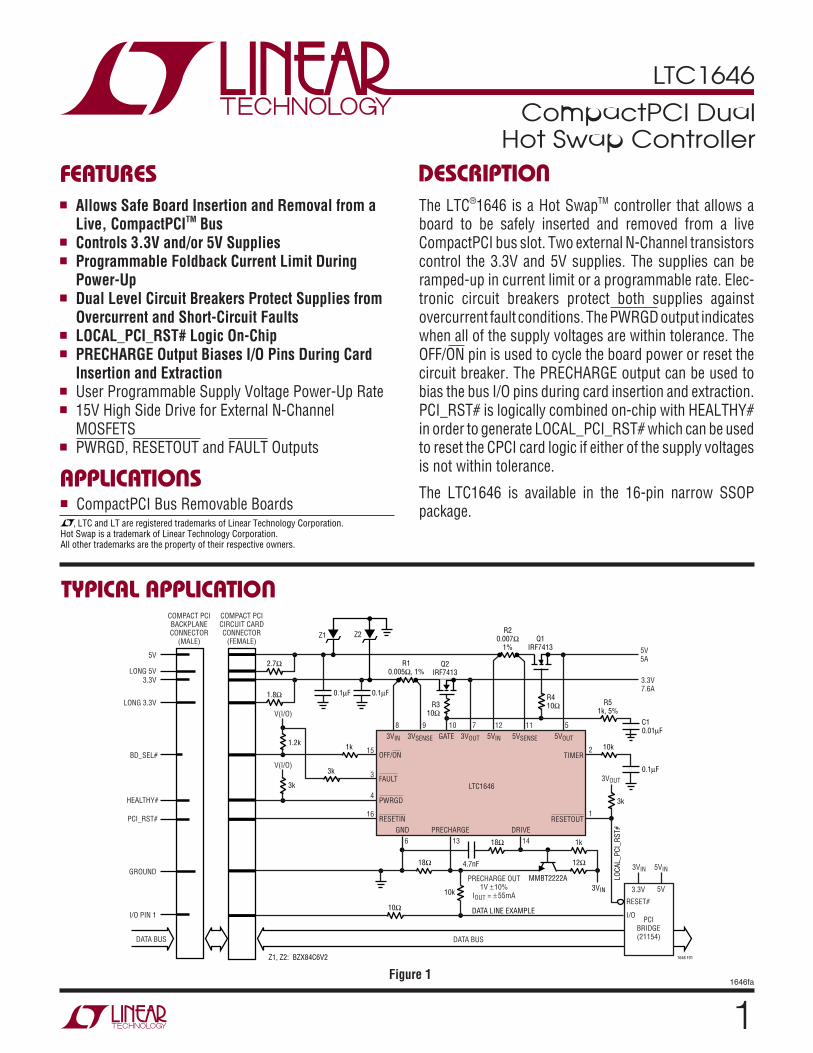
The LTC®1646 is a Hot SwapTM controller that allows aboard to be safely inserted and removed from a liveCompactPCI bus slot. Two external N-Channel transistorscontrol the 3.3V and 5V supplies. The supplies can beramped-up in current limit or a programmable rate. Elec-tronic circuit breakers protect both supplies againstovercurrent fault conditions. The PWRGD output indicateswhen all of the supply voltages are within tolerance. TheOFF/ON pin is used to cycle the board power or reset thecircuit breaker. The PRECHARGE output can be used tobias the bus I/O pins during card insertion and extraction.PCI_RST# is logically combined on-chip with HEALTHY#in order to generate LOCAL_PCI_RST# which can be usedto reset the CPCI card logic if either of the supply voltagesis not within tolerance.
The LTC1646 is available in the 16-pin narrow SSOPpackage.
Figure 1
MMBT2222A
4.7nF
18Ω
18Ω 12Ω
10Ω
2.7Ω
1.8ΩR3
10Ω
3k
R410Ω
3k
1k
R10.005Ω, 1%
R20.007Ω
1%
1k
R51k, 5%
10k
10k
3k
1.2k
3VIN
PRECHARGE OUT1V ±10%
IOUT = ± 55mA
3VIN
3VIN 3VSENSE 5VSENSE
3VOUT
3VOUT 5VOUT
3.3V
5VIN
5VIN
5V
RESET#
I/O PCIBRIDGE(21154)DATA BUSDATA BUS
V(I/O)
V(I/O)
0.1µF 0.1µF
0.1µF
C10.01µF
Q2IRF7413
Q1IRF7413
LOCA
L_PC
I_RS
T#
5V5A
3.3V7.6A
GATE
GND PRECHARGE DRIVERESETOUT
TIMEROFF/ON
FAULT
PWRGD
RESETIN
LTC1646
15
8 9 10 7 12 11 5
2
1
6 13 14
3
4
16
BD_SEL#
HEALTHY#
PCI_RST#
1646 F01
DATA LINE EXAMPLE
COMPACT PCIBACKPLANECONNECTOR
(MALE)
COMPACT PCICIRCUIT CARDCONNECTOR
(FEMALE)
5V
LONG 5V3.3V
LONG 3.3V
GROUND
I/O PIN 1
Z1, Z2: BZX84C6V2
Z2Z1
APPLICATIO SU
FEATURES
TYPICAL APPLICATIO
U
DESCRIPTIO
U
, LTC and LT are registered trademarks of Linear Technology Corporation.Hot Swap is a trademark of Linear Technology Corporation.All other trademarks are the property of their respective owners.

LTC1646
21646fa
SYMBOL PARAMETER CONDITIONS MIN TYP MAX UNITS
IDD V5VIN Supply Current OFF/ON = 0V 1.5 4 mA
VLKO Undervoltage Lockout 5VIN 2.3 2.50 2.7 V3VIN 2.3 2.55 2.7 V
VFB Foldback Current Limit Voltage VFB = (V5VIN – V5VSENSE), V5VOUT = 0V, TIMER = 0V 15 20 30 mVVFB = (V5VIN – V5VSENSE), V5VOUT = 4V, TIMER = 0V 50 55 65 mVVFB = (V3VIN – V3VSENSE), V3VOUT = 0V, TIMER = 0V 15 20 30 mVVFB = (V3VIN – V3VSENSE), V3VOUT = 2V, TIMER = 0V 50 55 65 mV
VCB Circuit Breaker Trip Voltage VCB = (V5VIN – V5VSENSE), V5VOUT = 5V, TIMER Open 50 56 65 mVVCB = (V3VIN – V3VSENSE), V3VOUT = 3.3V, TIMER Open 50 56 65 mV
tOC Overcurrent Fault Response Time (V5VIN – V5VSENSE) = 100mV, TIMER Open 10 21 30 µs(V3VIN – V3VSENSE) = 100mV, TIMER Open 10 21 30 µs
tSS Short-Circuit Fault Response Time (V5VIN – V5VSENSE) = 200mV, TIMER Open 0.145 1 µs(V3VIN – V3VSENSE) = 200mV, TIMER Open 0.145 1 µs
ICP GATE Pin Output Current OFF/ON = 0V, VGATE = 0V, TIMER = 0V –18 –13 –8 µAOFF/ON = 5V, VGATE = 5V, TIMER = 0V 80 200 300 µAOFF/ON = 0V, VGATE = 5V, FAULT = 0V, TIMER Open 4 7 12 mA
VGATE External Gate Voltage OFF/ON = 0V, IGATE = –1µA 12 15 16 V(GATE to GND) OFF/ON = 0V, V5VIN = 3.3V, IGATE = –1µA 11 13 15 V
VTH Power Good Threshold Voltage 3VOUT 2.8 2.9 3.0 V5VOUT 4.5 4.65 4.75 V
V3VONLY No 5V Input Mode Window Voltage V3VONLY = ⎪V5VIN – V3VIN⎪, V5VOUT = V3VOUT = 3.3V 50 120 200 mV
VIL Input Low Voltage OFF/ON, RESETIN, FAULT 0.8 V
ORDER PART NUMBER
TJMAX = 125°C, θJA = 135°C/W
Consult LTC Marketing for parts specified with wider operating temperature ranges.
LTC1646CGNLTC1646IGN
ABSOLUTE AXI U RATI GS
W WW U
PACKAGE/ORDER I FOR ATIOU UW
(Note 1)
ELECTRICAL CHARACTERISTICS The denotes the specifications which apply over the full operatingtemperature range, otherwise specifications are at TA = 25°C. V5VIN = 5V and V3VIN = 3.3V unless otherwise noted.
Supply Voltages: 5VIN, 3VIN ............................................... 10VInput Voltages: (Pins 15, 16) ..................... –0.3V to 10VOutput Voltages: (Pins 1, 3, 4) .................. –0.3V to 10VAnalog Voltages and Currents:
(Pin 9) .................................... –0.3V to (3VIN + 0.3V)(Pins 2, 5, 7, 11, 13, 14) ........ –0.3V to (5VIN + 0.3V)(Pin 10) .......................................................... ±20mA
Operating Temperature Range:LTC1646C ............................................... 0°C to 70°CLTC1646I .............................................–40°C to 85°C
Storage Temperature Range ..................–65°C to 150°CLead Temperature (Soldering, 10 sec).................. 300°C
TOP VIEW
GN PACKAGE16-LEAD PLASTIC SSOP
1
2
3
4
5
6
7
8
16
15
14
13
12
11
10
9
RESETOUT
TIMER
FAULT
PWRGD
5VOUT
GND
3VOUT
3VIN
RESETIN
OFF/ON
DRIVE
PRECHARGE
5VIN
5VSENSE
GATE
3VSENSE
GN PART MARKING16461646I
Order Options Tape and Reel: Add #TRLead Free: Add #PBF Lead Free Tape and Reel: Add #TRPBFLead Free Part Marking: http://www.linear.com/leadfree/

LTC1646
31646fa
SYMBOL PARAMETER CONDITIONS MIN TYP MAX UNITS
VIH Input High Voltage OFF/ON, RESETIN, FAULT 2 V
VTIMER TIMER Threshold Voltage VTIMER , FAULT = 0V 1.15 1.25 1.35 V
IIN OFF/ON Input Current OFF/ON = 5V ±0.08 ±10 µAOFF/ON = 0V ±0.08 ±10 µA
RESETIN Input Current RESETIN = 5V ±0.08 ±10 µARESETIN = 0V ±0.08 ±10 µA
5VSENSE Input Current 5VSENSE = 5V, 5VOUT = 0V 66 100 µA
3VSENSE Input Current 3VSENSE = 3.3V, 3VOUT = 0V 66 100 µA
3VIN Input Current 3VIN = 3.3V 460 1000 µA
5VOUT Input Current 5VOUT = 5V, OFF/ON = 0V 0.9 1.5 mA
3VOUT Input Current 3VOUT = 3.3V, OFF/ON = 0V 0.9 1.5 mA
ITIMER TIMER Pin Current OFF/ON = 0V, VTIMER = 0V –7 –5 –3 µAOFF/ON = 5V, VTIMER = 5V 6.6 mA
RDIS 5VOUT Discharge Impedance OFF/ON = 5V 120 220 Ω3VOUT Discharge Impedance OFF/ON = 5V 120 220 Ω
VOL Output Low Voltage FAULT, PWRGD, RESETOUT, I = 2mA 0.25 0.4 V
VPXG PRECHARGE Reference Voltage VPRECHARGE, V5VIN = 5V and 3.3V 0.90 1.00 1.10 V
ELECTRICAL CHARACTERISTICS The denotes the specifications which apply over the full operatingtemperature range, otherwise specifications are at TA = 25°C. V5VIN = 5V and V3VIN = 3.3V unless otherwise noted.
Note 1: Absolute Maximum Ratings are those values beyond which the lifeof a device may be impaired.
Note 2: All currents into device pins are positive; all currents out of devicepins are negative. All voltages are referenced to ground unless otherwisespecified.
TYPICAL PERFOR A CE CHARACTERISTICS
UW
5V Current Foldback Profile 3.3V Current Foldback Profile
OUTPUT VOLTAGE (V)0
OUTP
UT C
URRE
NT (A
)
2 4 5
1646 G01
1 3
12
11
10
9
8
7
6
5
4
3
2
1
0
RSENSE = 0.007Ω
1646 G02
12
11
10
9
8
7
6
5
4
3
2
1
0
OUTPUT VOLTAGE (V)0
OUTP
UT C
URRE
NT (A
)
2 4 51 3
RSENSE = 0.005Ω
–50 –25 0 25 50 75 100TEMPERATURE (°C)
SUPP
LY C
URRE
NT (m
A)
1646 G03
1.8
1.7
1.6
1.5
1.4
1.3
1.2
1.1
1.0
5VIN Supply Current vsTemperature

LTC1646
41646fa
TYPICAL PERFOR A CE CHARACTERISTICS
UW
5VIN Undervoltage LockoutVoltage vs Temperature
3VIN Undervoltage LockoutVoltage vs Temperature
5VIN Foldback Current LimitVoltage vs Temperature
–50 –25 0 25 50 75 100TEMPERATURE (°C)
UNDE
RVOL
TAGE
LOC
KOUT
VOL
TAGE
(V)
1646 G04
2.60
2.55
2.50
2.45
2.40
LOW-TO-HIGH TRANSITION
HIGH-TO-LOW TRANSITION
–50 –25 0 25 50 75 100TEMPERATURE (°C)
UNDE
RVOL
TAGE
LOC
KOUT
VOL
TAGE
(V)
1646 G05
2.60
2.55
2.50
2.45
2.40
LOW-TO-HIGH TRANSITION
HIGH-TO-LOW TRANSITION
–50 –25 0 25 50 75 100TEMPERATURE (°C)
FOLD
BACK
CUR
RENT
LIM
IT V
OLTA
GE (m
V)
1646 G06
60
50
40
30
20
10
0
5VOUT = 4V
5VOUT = 0V
–50 –25 0 25 50 75 100TEMPERATURE (°C)
FOLD
BACK
CUR
RENT
LIM
IT V
OLTA
GE (m
V)
1646 G07
60
50
40
30
20
10
0
3VOUT = 2V
3VOUT = 0V
–50 –25 0 25 50 75 100TEMPERATURE (°C)
CIRC
UIT
BREA
KER
TRIP
VOL
TAGE
(mV)
1646 G08
60
59
58
57
56
55
54
53
52
51
50–50 –25 0 25 50 75 100
TEMPERATURE (°C)
CIRC
UIT
BREA
KER
TRIP
VOL
TAGE
(mV)
1646 G09
60
59
58
57
56
55
54
53
52
51
50
–50 –25 0 25 50 75 100TEMPERATURE (°C)
OVER
CURR
ENT
FAUL
T RE
SPON
SE T
IME
(µs)
1646 G10
22.00
21.75
21.50
21.25
21.00
20.75
20.50
20.25
20.00–50 –25 0 25 50 75 100
TEMPERATURE (°C)
SHOR
T-CI
RCUI
T FA
ULT
RESP
ONSE
TIM
E (n
s)
1646 G11
170
160
150
140
130
120
110
100–50 –25 0 25 50 75 100
TEMPERATURE (°C)
GATE
CUR
RENT
(µA)
1646 G12
–10
–11
–12
–13
–14
–15
3VIN Foldback Current LimitVoltage vs Temperature
5VIN Circuit Breaker Trip Voltagevs Temperature
3VIN Circuit Breaker Trip Voltagevs Temperature
5VIN/3VIN Overcurrent FaultResponse Time vs Temperature
5VIN/3VIN Short-Circuit FaultResponse Time vs Temperature Gate Current vs Temperature

LTC1646
51646fa
TYPICAL PERFOR A CE CHARACTERISTICS
UW
Gate ISINK vs Temperature Gate Voltage vs TemperaturePower Good Threshold Voltage vsTemperature (3VOUT)
Power Good Threshold Voltage vsTemperature (5VOUT)
Timer Threshold Voltage vsTemperature
5VSENSE Input Current vsTemperature
3VSENSE Input Current vsTemperature 3VIN Input Current vs Temperature Timer Current vs Temperature
–50 –25 0 25 50 75 100TEMPERATURE (°C)
GATE
I SIN
K (m
A)
1646 G13
10
9
8
7
6
5
FAULT = 0V
–50 –25 0 25 50 75 100TEMPERATURE (°C)
GATE
VOL
TAGE
(V)
1646 G14
15.5
15.0
14.5
14.0
13.5
13.0
12.5
5VIN = 5VI = –1µA
5VIN = 3.3V
–50 –25 0 25 50 75 100TEMPERATURE (°C)
POW
ER G
OOD
THRE
SHOL
D VO
LTAG
E (V
)
1646 G15
3.00
2.95
2.90
2.85
2.80
–50 –25 0 25 50 75 100TEMPERATURE (°C)
POW
ER G
OOD
THRE
SHOL
D VO
LTAG
E (V
)
1646 G16
4.75
4.70
4.65
4.60
4.55
4.50–50 –25 0 25 50 75 100
TEMPERATURE (°C)
TIM
ER T
HRES
HOLD
VOL
TAGE
(V)
1646 G17
1.30
1.28
1.26
1.24
1.22
1.20–50 –25 0 25 50 75 100
TEMPERATURE (°C)
5VSE
NSE
INPU
T CU
RREN
T (µ
A)
1646 G18
70
69
68
67
66
65
64
63
62
61
60
–50 –25 0 25 50 75 100TEMPERATURE (°C)
3VSE
NSE
INPU
T CU
RREN
T (µ
A)
1646 G19
70
69
68
67
66
65
64
63
62
61
60–50 –25 0 25 50 75 100
TEMPERATURE (°C)
3VIN
INPU
T CU
RREN
T (µ
A)
1646 G20
480
475
470
465
460
455
450
445–50 –25 0 25 50 75 100
TEMPERATURE (°C)
TIM
ER C
URRE
NT (µ
A)
1646 G21
–4.00
–4.25
–4.50
–4.75
–5.00
–5.25
–5.50
–5.75
–6.00
LTC1646
61646fa
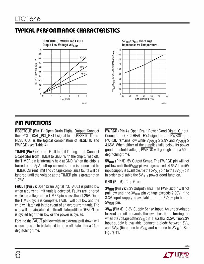
PWRGD (Pin 4) :Open Drain Power Good Digital Output.Connect the CPCI HEALTHY# signal to the PWRGD pin.PWRGD remains low while V3VOUT ≥ 2.9V and V5VOUT ≥4.65V. When either of the supplies falls below its powergood threshold voltage, PWRGD will go high after a 50µsdeglitching time.
5VOUT (Pin 5): 5V Output Sense. The PWRGD pin will notpull low until the 5VOUT pin voltage exceeds 4.65V. If no 5Vinput supply is available, tie the 5VOUT pin to the 3VOUT pinin order to disable the 5VOUT power good function.
GND (Pin 6): Chip Ground
3VOUT (Pin 7): 3.3V Output Sense. The PWRGD pin will notpull low until the 3VOUT pin voltage exceeds 2.90V. If no3.3V input supply is available, tie the 3VOUT pin to the5VOUT pin.
3VIN (Pin 8): 3.3V Supply Sense Input. An undervoltagelockout circuit prevents the switches from turning onwhen the voltage at the 3VIN pin is less than 2.5V. If no 3.3Vinput supply is available, connect a diode between 5VINand 3VIN (tie anode to 5VIN and cathode to 3VIN ). SeeFigure 11.
RESETOUT (Pin 1): Open Drain Digital Output. Connectthe CPCI LOCAL_PCI_RST# signal to the RESETOUT pin.RESETOUT is the logical combination of RESETIN andPWRGD (see Table 4).
TIMER (Pin 2): Current Fault Inhibit Timing Input. Connecta capacitor from TIMER to GND. With the chip turned off,the TIMER pin is internally held at GND. When the chip isturned on, a 5µA pull-up current source is connected toTIMER. Current limit and voltage compliance faults will beignored until the voltage at the TIMER pin is greater than1.25V.
FAULT (Pin 3): Open Drain Digital I/O. FAULT is pulled lowwhen a current limit fault is detected. Faults are ignoredwhile the voltage at the TIMER pin is less than 1.25V. Oncethe TIMER cycle is complete, FAULT will pull low and thechip will latch off in the event of an overcurrent fault. Thechip will remain latched in the off state until the OFF/ON pinis cycled high then low or the power is cycled.
Forcing the FAULT pin low with an external pull-down willcause the chip to be latched into the off state after a 21µsdeglitching time.
TYPICAL PERFOR A CE CHARACTERISTICS
UW
RESETOUT, PWRGD and FAULTOutput Low Voltage vs ISINK
5VOUT/3VOUT DischargeImpedance vs Temperature
–50 –25 0 25 50 75 100TEMPERATURE (°C)
3VOU
T/5V
OUT
DISC
HARG
E IM
PEDA
NCE
(Ω)
1646 G23
180
160
140
120
100
80
60
40
20
00 1 2 3 4 5
ISINK (mA)
OUTP
UT L
OW V
OLTA
GE (V
)
1646 G22
1.0
0.9
0.8
0.7
0.6
0.5
0.4
0.3
0.2
0.1
0
90°C
25°C
–45°C
UUU
PI FU CTIO S

LTC1646
71646fa
UUU
PI FU CTIO S3VSENSE (Pin 9): 3.3V Current Limit Set. With a senseresistor placed in the supply path between 3VIN and3VSENSE, the GATE pin voltage will be adjusted to maintaina constant voltage across the sense resistor and a con-stant current through the switch while the TIMER pinvoltage is less than 1.25V. A foldback feature makes thecurrent limit decrease as the voltage at the 3VOUT pinapproaches GND.
When the TIMER pin voltage exceeds 1.25V, the circuitbreaker function is enabled. If the voltage across the senseresistor exceeds 56mV, the circuit breaker is tripped aftera 21µs time delay. In the event the sense resistor voltageexceeds 150mV, the circuit breaker trips immediately andthe chip latches off. To disable the 3.3V current limit,3VSENSE and 3VIN can be shorted together.
GATE (Pin 10): High Side Gate Drive for the External 3.3Vand 5V N-Channel pass transistors. Requires an externalseries RC network for the current limit loop compensationand setting the minimum ramp-up rate. During power-up,the slope of the voltage rise at the GATE is set by the 13µAcurrent source connected to the internal charge pump andthe external capacitor connected to GND or by the 3.3V or5V current limit and the bulk capacitance on the 3VOUT or5VOUT supply lines. During power-down, the slope of theramp down voltage is set by the 200µA current sourceconnected to GND and the external GATE capacitor.
The voltage at the GATE pin will be modulated to maintaina constant current when either the 3V or 5V supplies gointo current limit while the TIMER pin voltage is less than1.25V. If a current fault occurs after the TIMER pin voltageexceeds 1.25V, the GATE pin is immediately pulled toGND.
5VSENSE (Pin 11): 5V Current Limit Set. With a senseresistor placed in the supply path between 5VIN and5VSENSE, the GATE pin voltage will be adjusted to maintaina constant voltage across the sense resistor and a con-stant current through the switch while the TIMER pinvoltage is less than 1.25V. A foldback feature makes thecurrent limit decrease as the voltage at the 5VOUT pinapproaches GND.
When the TIMER pin voltage is greater than 1.25V, thecircuit breaker function is enabled. If the voltage acrossthe sense resistor exceeds 56mV but is less than 150mV,the circuit breaker is tripped after a 21µs time delay. In theevent the sense resistor voltage exceeds 150mV, thecircuit breaker trips immediately and the chip latches off.To disable the 5V current limit, short 5VSENSE and 5VINtogether.
5VIN (Pin 12): 5V Supply Sense Input. An undervoltagelockout circuit prevents the GATE pin voltage fromramping up when the voltage at the 5VIN pin is less than2.5V. If no 5V input supply is available, tie the 5VIN pin tothe 3VIN pin.
PRECHARGE (Pin 13): Precharge Monitor Input. An on-chip error amplifier with a 1V reference servos the DRIVEpin voltage to keep the precharge node at 1V. If theprecharge function is not being used, tie the PRECHARGEpin to GND.
DRIVE (Pin 14): Precharge Base Drive Output. Providesbase drive for an external NPN emitter-follower which inturn biases the PRECHARGE node. If the precharge func-tion is not being used, allow the DRIVE pin to float.
OFF/ON (Pin 15): Digital Input. Connect the CPCI BD_SEL#signal to the OFF/ON pin. When the OFF/ON pin is pulledlow, the GATE pin is pulled high by a 13µA current source.When the OFF/ON pin is pulled high the GATE pin will bepulled to ground by a 200µA current source.
The OFF/ON pin is also used to reset the electronic circuitbreaker. If the OFF/ON pin is cycled high and low followingthe trip of the circuit breaker, the circuit breaker is reset,and a normal power-up sequence will occur.
RESETIN (Pin 16): Digital Input. Connect the CPCIPCI_RST# signal to the RESETIN pin. Pulling RESETIN lowwill cause the RESETOUT pin to pull low.

LTC1646
81646fa
TEST DIAGRA
W
TI I G DIAGRA S
WU W
V3VONLY No 5V Input Mode Window Voltage
tOC Overcurrent Fault Detect
tSC Short-Circuit Fault Detect
5VOR 3.3V
100mV
FAULT
tOC
1V
V5VSENSEOR
V3VSENSE
FALL TIME ≤ 1µs, 5VIN = 5V, 3VIN = 3.3V
1646 T02
5VOR 3.3V
200mV
FAULT
tSC
1V
V5VSENSEOR
V3VSENSE
FALL TIME ≤ 30ns, 5VIN = 5V, 3VIN = 3.3V
1646 T03
–V3VONLY
V3VONLY
5V
0VPWRGD
V5VIN3.3V
1646 T01
V3VONLY = ⎟ 5VIN – 3VIN ⎢ 5VOUT = 3VOUT = 3.3V, 3VIN = 3.3V
LTC1646
91646fa
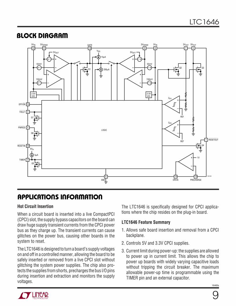
Hot Circuit Insertion
When a circuit board is inserted into a live CompactPCI(CPCI) slot, the supply bypass capacitors on the board candraw huge supply transient currents from the CPCI powerbus as they charge up. The transient currents can causeglitches on the power bus, causing other boards in thesystem to reset.
The LTC1646 is designed to turn a board’s supply voltageson and off in a controlled manner, allowing the board to besafely inserted or removed from a live CPCI slot withoutglitching the system power supplies. The chip also pro-tects the supplies from shorts, precharges the bus I/O pinsduring insertion and extraction and monitors the supplyvoltages.
BLOCK DIAGRA
W
TIMER 2
3VOUT
7
5VOUT
5
–
++–
Q2 Q3200µA
13µA
GATE
5VOUT
55mV
150mV
VGG
10
5VSENSE
11
5VIN
12
–
+
+–
+–
2.5VUVL
–
+ +–
3VOUT
55mV
150mV
CP3
REF
3VSENSE
9
3VIN
8
RESETOUT1
–
+
–
+
+–
+–
2.5VUVL
Q4
1V
CP4
REF
–
+
–
+
RESETIN 16
PWRGD 4
Q6
FAULT 3
Q7
OFF/ON 15
5µA
5Vin
GND6
DRIVE14
PRECHARGE
1646 BD13
LOGIC
Q1
Q5
APPLICATIO S I FOR ATIO
WU UU
The LTC1646 is specifically designed for CPCI applica-tions where the chip resides on the plug-in board.
LTC1646 Feature Summary
1. Allows safe board insertion and removal from a CPCIbackplane.
2. Controls 5V and 3.3V CPCI supplies.
3. Current limit during power-up: the supplies are allowedto power up in current limit. This allows the chip topower up boards with widely varying capacitive loadswithout tripping the circuit breaker. The maximumallowable power-up time is programmable using theTIMER pin and an external capacitor.

LTC1646
101646fa
APPLICATIO S I FOR ATIO
WU UU
The main 3.3V and 5V inputs to the LTC1646 come fromthe medium length power pins. The long 3.3V, 5V connec-tor pins are shorted to the medium length 5V and 3.3Vconnector pins on the CPCI plug-in card and provide earlypower for the LTC1646’s precharge circuitry, the V(I/O)pull-up resistors and the PCI bridge chip. The BD_SEL#signal is connected to the OFF/ON pin while the PWRGDpin is connected to the HEALTHY# signal. The HEALTHY#signal is combined with the PCI_RST# signal on-chip togenerate the LOCAL_PCI_RST# signal which is availableat the RESETOUT pin.
The power supplies are controlled by placing externalN-channel pass transistors in the 3.3V and 5V powerpaths.
Resistors R1 and R2 provide current fault detection andR5 and C1 provide current control loop compensation.Resistors R3 and R4 prevent high frequency oscillationsin Q1 and Q2.
When the CPCI card is inserted, the long 5V and 3.3Vconnector pins and GND pins make contact first. TheLTC1646’s precharge circuit biases the bus I/O pins to 1Vduring this stage of the insertion (Figure 2). The 5V and3.3V medium length pins make contact during the nextstage of insertion, but the slot power is disabled as longas the OFF/ON pin is pulled high by the 1.2k pull-upresistor to V(I/O). During the final stage of board insertion,the BD_SEL# short connector pin makes contact and theOFF/ON pin can be pulled low. This enables the passtransistors to turn on and a 5µA current source is con-nected to the TIMER pin.
The current in each pass transistor increases until itreaches the current limit for each supply. The 5V and 3.3Vsupplies are then allowed to power up based on one of thefollowing power-up rates:
dVdt
AC
orI
Cor
IC
LIMIT V
LOAD VOUT
LIMIT V
LOAD VOUT= µ = =13
15
5
3
3, ,( )
( )
( )
( )(1)
whichever is slower.
Current limit faults are ignored while the TIMER pinvoltage is ramping up and is less than 1.25V. Once bothsupply voltages are within tolerance, HEALTHY# will pulllow and LOCAL_PCI_RST# is free to follow PCI_RST#.
4. Programmable foldback current limit: a programmableanalog current limit with a value that depends on theoutput voltage. If the output is shorted to ground, thecurrent limit drops to keep power dissipation andsupply glitches to a minimum.
5. Dual-level, programmable 5V and 3.3V circuit breakers:this feature is enabled when the TIMER pin voltageexceeds 1.25V. If either supply exceeds current limitfor more than 21µs, the circuit breaker will trip, thesupplies will be turned off, and the FAULT pin is pulledlow. In the event that either supply exceeds three timesthe set current limit, all supplies will be turned off andthe FAULT pin is pin is pulled low without delay.
6. 15V high side drive for external 3.3V and 5V N-channelMOSFETs.
7. PWRGD output: monitors the voltage status of thesupply voltages.
8. PCI_RST# combined on-chip with HEALTHY# to createLOCAL_PCI_RST# output. If HEALTHY# deasserts,LOCAL_PCI_RST# is asserted independent ofPCI_RST#.
9. Precharge output: on-chip reference and amplifier pro-vide 1V for biasing bus I/O connector pins during CPCIcard insertion and extraction.
10. Space saving 16-pin SSOP package.
PCI Power Requirements
CPCI systems may require up to four power rails: 5V, 3.3V,12V and –12V. The LTC1646 is designed for CPCI applica-tions which only use the 5V and/or 3.3V supplies. Thetolerance of the supplies as measured at the componentson the plug-in card is summarized in Table 1.Table 1. PCI Power Supply RequirementsSUPPLY TOLERANCE CAPACITIVE LOAD
5V 5V ±5% <3000µF
3.3V 3.3V ±0.3V <3000µF
Power-Up Sequence
The LTC1646 is specifically designed for hot swappingCPCI boards. The typical application is shown in Figure 1.

LTC1646
111646fa
Power-Down Sequence
When BD_SEL# is pulled high, a power-down sequencebegins (Figure 3).
Internal switches are connected to each of the outputsupply voltage pins to discharge the bypass capacitors toground. The TIMER pin (Pin 2) is immediately pulled low.The GATE pin (Pin 10) is pulled down by a 200µA currentsource to prevent the load currents on the 3.3V and 5Vsupplies from going to zero instantaneously in order toprevent glitching the power supply voltages. When eitherof the output voltages dips below its threshold, HEALTHY#pulls high and LOCAL_PCI_RST# will be asserted low.
Once the power-down sequence is complete, the CPCIcard may be removed from the slot. During extraction, theprecharge circuit will continue to bias the bus I/O pins at1V until the 5V and 3.3V long connector pin connectionsare separated.
Timer
During a power-up sequence, a 5µA current source isconnected to the TIMER pin and current limit faults areignored until the voltage exceeds 1.25V. This feature
allows the chip to power up CPCI boards with widelyvarying capacitive loads on the supplies. The power-uptime for either of the two outputs is given by:
t XVC XV
I ION OUTLOAD XVOUT OUT
LIMIT XVOUT LOAD XVOUT( ) •
•–
( )
( ) ( )= 2 (2)
Where XVOUT = 5VOUT or 3VOUT. For example, forCLOAD(5VOUT) = 2000µF, ILIMIT = 7A, and ILOAD = 5A, the5VOUT turn-on time will be ~10ms. By substituting thevariables in Equation 2 with the appropriate values, theturn-on time for the 3VOUT output can also be calculated.The timer period should be set longer than the maximumsupply turn-on time but short enough to not exceed themaximum safe operating area of the pass transistor duringa short-circuit. The timer period for the LTC1646 is givenby:
tC V
ATIMERTIMER=
µ• .1 25
5 (3)
As a design aid, the timer period as a function of the timingcapacitor using standard values from 0.01µF to 1µF isshown in Table 2.
20ms/DIV
GATE10V/DIV
5VOUT3VOUT5V/DIV
TIMER5V/DIV
BD_SEL#5V/DIV
HEALTHY#5V/DIV
LCL_PCI_RST#5V/DIV
PRECHARGE5V/DIV
1646 F02
GATE10V/DIV
5VOUT3VOUT5V/DIV
TIMER5V/DIV
BD_SEL#5V/DIV
HEALTHY#5V/DIV
LCL_PCI_RST#5V/DIV
PRECHARGE5V/DIV
10ms/DIV 1646 F03
Figure 2. Normal Power-Up Sequence Figure 3. Normal Power-Down Sequence
APPLICATIO S I FOR ATIO
WU UU

LTC1646
121646fa
APPLICATIO S I FOR ATIO
WU UUFigure 4. Power-Up into a Short on 3.3V Output
GATE5V/DIV
5VOUT3VOUT2V/DIV
TIMER1V/DIV
BD_SEL#5V/DIV
LCL_PCI_RST#5V/DIV
HEALTHY#5V/DIV
FAULT5V/DIV
10ms/DIV 1646 F04
Table 2. tTIMER vs CTIMER
CTIMER tTIMER CTIMER tTIMER
0.01µF 2.5ms 0.22µF 55ms
0.022µF 5.5ms 0.33µF 82.5ms
0.033µF 8.25ms 0.47µF 118ms
0.047µF 11.8ms 0.68µF 170ms
0.068µF 17ms 0.82µF 205ms
0.082µF 20.5ms 1µF 250ms
0.1µF 25ms
The TIMER pin is immediately pulled low when BD_SEL#goes high.
Short-Circuit Protection
During a normal power-up sequence, if the TIMER pin isdone ramping and a supply is still in current limit, all of thepass transistors will be immediately turned off and FAULT(Pin 3) will be pulled low as shown in Figure 4.
In order to prevent excessive power dissipation in the passtransistors and to prevent voltage spikes on the suppliesduring short-circuit conditions, the current limit on eachsupply is designed to be a function of the output voltage.As the output voltage drops, the current limit decreases.
Unlike a traditional circuit breaker function where hugecurrents can flow before the breaker trips, the currentfoldback feature assures that the supply current will bekept at a safe level and prevents voltage glitches at theinput supply when powering up into a short circuit.
After power-up (TIMER pin voltage >1.25V), the 5V and3.3V supplies are protected from overcurrent and short-circuit conditions by dual-level circuit breakers. If thesense resistor voltage of either supply current exceeds56mV but is less than 150mV, an internal timer is started.If the supply is still overcurrent after 21µs, the circuitbreaker trips and both supplies are turned off (Figure 5).
5VIN –5VSENSE50mV/DIV
GATE10V/DIV
FAULT5V/DIV
10µs/DIV 1646 F05
Figure 5. Overcurrent Fault on 5V
If a short-circuit occurs and the sense resistor voltage ofeither supply current exceeds 150mV, the circuit breakerstrip without delay and the chip latches off (Figure 6). Thechip will stay in the latched-off state until OFF/ON (Pin 15)is cycled high then low, or the 5VIN (Pin 12) power supplyis cycled.
The current limit and the foldback current level for the 5Vand 3.3V outputs are both a function of the external senseresistor (R1 for 3VOUT and R2 for 5VOUT, see Figure 1). Asshown in Figure 1, a sense resistor is connected between

LTC1646
131646fa
APPLICATIO S I FOR ATIO
WU UU
5VIN (Pin 12) and 5VSENSE (Pin 11) for the 5V supply. Forthe 3.3V supply, a sense resistor is connected between3VIN (Pin 8) and 3VSENSE (Pin 9). The current limit and thecurrent foldback current level are given by Equations 4and 5:
ImV
R
ImV
R
LIMIT XVOUTSENSE XVOUT
FOLDBACK XVOUTSENSE XVOUT
( )( )
( )( )
=
=
55
20 (5)
where XVOUT = 5VOUT or 3VOUT.
As a design aid, the current limit and foldback level forcommonly used values for RSENSE is shown in Table 3.Table 3. ILIMIT(XVOUT) and IFOLDBACK(XVOUT) vs RSENSE
RSENSE (Ω) ILIMIT(XVOUT) IFOLDBACK(XVOUT)
0.005 11A 4A
0.006 9.2A 3.3A
0.007 7.9A 2.9A
0.008 6.9A 2.5A
0.009 6.1A 2.2A
0.01 5.5A 2A
where XVOUT = 3VOUT or 5VOUT.
5VIN –5VSENSE100mV/DIV
GATE10V/DIV
FAULT5V/DIV
5µs/DIV 1646 F06
(4)
Figure 6. Short-Circuit Fault on 5V
43
21
+–
5VIN
5VIN
RSENSE
5VSENSE
VCB
VCB(MAX) = 65mVVCB(NOM) = 56mVVCB(MIN) = 50mV
12 11
ILOAD(MAX)
LTC1646*
*ADDITIONAL DETAILS OMITTED FOR CLARITY
1646 F07
– +
Figure 7. Circuit Breaker EquivalentCircuit for Calculating RSENSE
Calculating RSENSE
An equivalent circuit for one of the LTC1646’s circuitbreakers useful in calculating the value of the senseresistor is shown in Figure 7. To determine the mostappropriate value for the sense resistor first requires themaximum current required by the load under worst-caseconditions.
Two other parameters affect the value of the sense resis-tor. First is the tolerance of the LTC1646’s circuit breakerthreshold. The LTC1646’s nominal circuit breakerthreshold is VCB(NOM) = 56mV; however, it exhibits a–6mV/+9mV tolerance due to process variations. Secondis the tolerance (RTOL) in the sense resistor. Senseresistors are available in RTOLs of ±1%, ±2% and ±5%and exhibit temperature coefficients of resistance (TCRs)between ±75ppm/°C and ±100ppm/°C. How the senseresistor changes as a function of temperature depends onthe I2R power being dissipated by it.
The first step in calculating the value of RSENSE is based onITRIP(MAX) and the lower limit for the circuit breakerthreshold, VCB(MIN). The maximum value for RSENSE in thiscase is expressed by Equation 6:
RV
ISENSE MAXCB MIN
TRIP MAX( )
( )
( )= (6)
The second step is to determine the nominal value of thesense resistor which is dependent on its tolerance

LTC1646
141646fa
APPLICATIO S I FOR ATIO
WU UU
(RTOL = ±1%, ±2% or ±5%) and standard sense resistorvalues. Equation 7 can be used to calculate the nominalvalue from the maximum value found by Equation 6:
RR
RTOLSENSE NOMSENSE MAX
( )( )=
+ ⎛⎝⎜
⎞⎠⎟
1100
(7)
Often, the result of Equation 7 may not yield a standardsense resistor value. In this case, two sense resistors withthe same RTOL can be connected in parallel to yieldRSENSE(NOM).
The last step requires calculating a new value forITRIP(MAX)(ITRIP(MAX, NEW)) based on a minimum value forRSENSE (RSENSE(MIN)) and the upper limit for the circuitbreaker threshold, VCB(MAX). Should the calculated valuefor ITRIP(MAX, NEW) be much greater than the design valuefor ITRIP(MAX), a larger sense resistor value should beselected and the process repeated. The new value forITRIP(MAX, NEW) is given by Equation 8:
IV
R
where R RRTOL
TRIP MAX NEWCB MAX
SENSE MIN
SENSE MIN SENSE NOM
( , )( )
( )
( ) ( )
( )
• –
=
= ⎛⎝⎜
⎞⎠⎟
⎡
⎣⎢
⎤
⎦⎥
8
1100
Example: A 5V supply exhibits a nominal 5A load with amaximum load current of 6.8A (ILOAD(MAX) = 6.8A), andsense resistors with ±5% RTOL will be used. According toEquation 6, VCB(MIN) = 50mV and RSENSE(MAX) is given by:
RV
ImV
ASENSE MAXCB MIN
TRIP MAX( )
( )
( ) ..= = = Ω50
6 80 0074
The nominal sense resistor value is (Equation 7):
RR
RTOLSENSE NOMSENSE MAX
( )( ) .
.=+ ⎛
⎝⎜⎞⎠⎟
= Ω
+ ⎛⎝⎜
⎞⎠⎟
= Ω1
100
0 0074
15
100
0 007
And the new current-limit trip point is Equation 8:
IV
R
V
RRTOL
mVA
TRIP MAX NEWCB MAX
SENSE MIN
CB MAX
SENSE N M
( , )( )
( )
( )
( ) • –.
.
= =
⎛⎝⎜
⎞⎠⎟
⎡
⎣⎢
⎤
⎦⎥
= =
0 1100
650 0065
9 8
Since ITRIP(MAX, NEW) > ILOAD(MAX), a larger value forRSENSE should be selected and the process repeated againto lower ITRIP(MAX, NEW) without substantially affectingILOAD(MAX).
Output Voltage Monitor
The status of both 5V and 3.3V output voltages is moni-tored by the power good function. In addition, the PCI_RST#signal is logically combined on-chip with the HEALTHY#signal to create LOCAL_PCI_RST# (see Table 4).Table 4. LOCAL_PCI_RST# Truth Table
PCI_RST# HEALTHY# LOCAL_PCI_RST#
LO LO LO
LO HI LO
HI LO HI
HI HI LO
If either of the output voltages drop below the power goodthreshold for more than 50µs, the HEALTHY# signal will bepulled high and the LOCAL_PCI_RST# signal will be pulledlow.
Precharge
The PRECHARGE input and DRIVE output pins are in-tended for use in generating the 1V precharge voltage thatis used to bias the bus I/O connector pins during boardinsertion. The LTC1646 is also capable of generatingprecharge voltages other than 1V. Figure 8 shows a circuitthat can be used in applications requiring a prechargevoltage less than 1V. The circuit in Figure 9 can be used forapplications that need precharge voltages greater than 1V.Table 5 lists suggested resistor values for R1 and R2 vsprecharge voltage for the application circuits shown inFigures 8 and 9.
LTC1646
151646fa
Figure 10. 3.3V Supply Only Typical Application
Figure 8. Precharge Voltage <1V Application Circuit
APPLICATIO S I FOR ATIO
WU UU
MMBT2222A
4.7nF 18Ω18Ω
10Ω
10Ω
3k
3k
1k
0.005Ω1%
1k
12Ω
1k
10k
1k
3k
1.2k
3VIN
PRECHARGE OUT1V ±10%
IOUT = ± 55mA
3VIN
3VIN 3VSENSE 5VSENSE
3VOUT
3VOUT 5VOUT
3.3V
5VIN
RESET#I/O
PCIBRIDGE(21154)DATA BUS
DATA LINE EXAMPLE
V(I/O)
V(I/O)
0.1µF
0.1µF
0.010µF
IRF7413
LOCA
L_PC
I_RS
T#
3.3VOUT7.6A
GATE
GND PRECHARGE DRIVE
RESETOUT
TIMEROFF/ON
FAULT
PWRGD
RESETIN
LTC1646
15
8 9 10 7 12 11 5
2
1
6 13 14
3
4
16
1646 F10Z1: BZX84C6V2
Z1
DATA BUS
BD_SEL#
HEALTHY#
PCI_RST#
COMPACT PCIBACKPLANECONNECTOR
(MALE)
COMPACT PCICIRCUIT CARDCONNECTOR
(FEMALE)
3.3V
LONG 3.3V
GROUND
I/O PIN 1
43
21
1.8Ω
MMBT2222A
4.7nF 18Ω
R1 R2
1k
12Ω
3VINPRECHARGE OUT
1646 F08
GND PRECHARGE DRIVE
LTC1646*
6 13 14
*ADDITIONAL DETAILS OMITTED FOR CLARITY
VPRECHARGE = • 1VR1
R1 + R2
MMBT2222A
4.7nF 18Ω
R1 R2
1k
12Ω
3VINPRECHARGE OUT
1646 F09
GND PRECHARGE DRIVE
LTC1646*
6 13 14
*ADDITIONAL DETAILS OMITTED FOR CLARITY
VPRECHARGE = • 1VR1 + R2
R1
Figure 9. Precharge Voltage >1V Application Circuit
Other CompactPCI Applications
The LTC1646 can be easily configured for applicationswhere no 5V supply is present by simply tying the 5VIN and5VSENSE pins to the 3VIN pin and tying the 5VOUT pin to the3VOUT pin (Figure 10).
Table 5. R1 and R2 Resistor Values vs Precharge VoltageVPRECHARGE R1 R2 VPRECHARGE R1 R2
1.5V 18Ω 9.09Ω 0.9V 16.2Ω 1.78Ω
1.4V 18Ω 7.15Ω 0.8V 14.7Ω 3.65Ω1.3V 18Ω 5.36Ω 0.7V 12.1Ω 5.11Ω1.2V 18Ω 3.65Ω 0.6V 11Ω 7.15Ω1.1V 18Ω 1.78Ω 0.5V 9.09Ω 9.09Ω1V 18Ω 0Ω

LTC1646
161646fa
Figure 11. 5V Supply Only Typical Application
Figure 12. BD_SEL# Pushbutton Toggle Switch
APPLICATIO S I FOR ATIO
WU UU
If no 3.3V supply is present, Figure 11 illustrates how theLTC1646 should be configured. First, 3VSENSE (Pin 9) isconnected to 3VIN (Pin 8), 3VOUT (Pin 7) is connected to5VOUT (Pin 5) and the LTC1646’s 3VIN pin is connectedthrough a diode (BAV16W) to 5VIN.
For applications where the BD_SEL# connector pin istypically grounded on the backplane, the circuit inFigure 12 allows the LTC1646 to be reset simply bypressing a pushbutton switch on the CPCI plug-in board.This arrangement eliminates the requirement to extractand reinsert the CPCI board in order to reset the LTC1646’scircuit breakers.
Overvoltage Transient Protection
Good engineering practice calls for bypassing the supplyrail of any analog circuit. Bypass capacitors are oftenplaced at the supply connection of every active device, inaddition to one or more large-value bulk bypass capacitorsper supply rail. If power is connected abruptly, the largebypass capacitors slow the rate of rise of the supplyvoltage and heavily damp any parasitic resonance of leador PC trace inductance working against the supply bypasscapacitors.
The opposite is true for LTC1646 Hot Swap circuitsmounted on plug-in cards. In most cases, there is nosupply bypass capacitor present on the powered 3.3V or5V side of the MOSFET switch. An abrupt connection,produced by inserting the board into a backplane connec-tor, results in a fast rising edge applied on the 3.3V and the5V line of the LTC1646.
2.7Ω10Ω
0.007Ω
1k
3VIN 3VSENSE 5VSENSE GATE 5VOUT 3VOUT5VIN
5VIN
0.1µF0.01µF
IRF74135VOUT
LTC1646
8 9 12 11 10 5 7
6
BAV16W
1646 F11
GND
COMPACT PCIBACKPLANECONNECTOR
(MALE)
COMPACT PCICIRCUIT CARDCONNECTOR
(FEMALE)
GND
5V
LONG5V
43
21
Z1: BZX84C6V2
Z1
BD_SEL#
1k100Ω
LONG GND
15
6
OFF/ON
LTC1646
GND
V(I/0)
PUSH-BUTTONSWITCH
1646 F12
1.2k
COMPACT PCIBACKPLANECONNECTOR
(MALE)
COMPACT PCICIRCUIT CARDCONNECTOR
(FEMALE)

LTC1646
171646fa
APPLICATIO S I FOR ATIO
WU UU
Figure 14. Recommended Layout forTransient Protection Components
1 2 3 4 5 6 7 8
16 15 14 13 12 11 10 9
VIAS TOGND PLANE
3VINGND
LTC1646*
*ADDITIONAL DETAILS OMITTED FOR CLARITYDRAWING IS NOT TO SCALE! 1646 F14
5VIN
TZ1
TZ2
C2
C3
Since there is no bulk capacitance to damp the parasitictrace inductance, supply voltage transients excite para-sitic resonant circuits formed by the power MOSFETcapacitance and the combined parasitic inductance fromthe wiring harness, the backplane and the circuit boardtraces. These ringing transients appear as a fast edge onthe 3.3V or 5V supply, exhibiting a peak overshoot to 2.5times the steady-state value followed by a damped sinu-soidal response whose duration and period is dependenton the resonant circuit parameters. Since the absolutemaximum supply voltage of the LTC1646 is 10V, transientprotection against 3.3V and 5V supply voltage spikes andringing is highly recommended.
In these applications, there are two methods for eliminat-ing these supply voltage transients: using Zener diodes toclip the transient to a safe level and snubber networks.Snubbers are RC networks whose time constants arelarge enough to safely damp the inductance of the board’sparasitic resonant circuits. As a starting point, the shuntcapacitors in these networks are chosen to be 10× to 100×the power MOSFET’s COSS under bias. The value of theseries resistor (R6 and R7 in Figure 13) is then chosen tobe large enough to damp the resulting series R-L-C circuitand typically ranges from 1Ω to 10Ω. Note that in all
Figure 13. Place Transient Protection Device Close to the LTC1646
C10.01µF
C20.1µF
C30.1µF
3VIN
VIN23.3V
VIN15V
3VSENSE
8
3VOUT
7
5VIN
12
5VOUT
5
5VSENSE
119
GATE
10
R310Ω
R410Ω
5VOUTAT 5A
3VOUTAT 7.6A
R51k
R10.005Ω
Q2IRF7413
Q1IRF7413
R20.007Ω
Z1 Z2LTC1646**
1646 F13
GND
6Z1, Z2: BZX84C6V2**ADDITIONAL DETAILS OMITTED FOR CLARITY
R6 2.7ΩLONG 5V
R7 1.8ΩLONG 3.3V
LTC1646 circuit schematics, Zener diodes and snubbernetworks have been added to each 3.3V and 5V supply railand should be used always. These protection networksshould be mounted very close to the LTC1646’s supplyvoltage using short lead lengths to minimize lead induc-tance. This is shown schematically in Figure 13 and arecommended layout of the transient protection devicesaround the LTC1646 is shown in Figure 14.

LTC1646
181646fa
Table 6. N-Channel Power MOSFET Selection GuideCURRENT LEVEL (A) PART NUMBER DESCRIPTION MANUFACTURER
0 to 2 MMDF3N02HD Dual N-Channel SO-8 ON SemiconductorRDS(ON) = 0.1Ω
2 to 5 MMSF5N02HD Single N-Channel SO-8 ON SemiconductorRDS(ON) = 0.025Ω
5 to 10 MTB50N06V Single N-Channel DD Pak ON SemiconductorRDS(ON) = 0.028Ω
5 to 10 IRF7413 Single N-Channel SO-8 International RectifierRDS(ON) = 0.01Ω
5 to 10 Si4410DY Single N-Channel SO-8 Vishay-SiliconixRDS(ON) = 0.01Ω
Table 7. Sense Resistor Selection GuideCURRENT LIMIT VALUE PART NUMBER DESCRIPTION MANUFACTURER
1A LR120601R055F 0.055Ω, 0.5W, 1% Resistor IRC-TTWSL1206R055 Vishay-Dale
2A LR120601R028F 0.028Ω, 0.5W, 1% Resistor IRC-TTWSL1206R028 Vishay-Dale
5A LR120601R011F 0.011Ω, 0.5W, 1% Resistor IRC-TTWSL2010R011 Vishay-Dale
7.6A WSL2512R007 0.007Ω, 1W, 1% Resistor Vishay-Dale
10A WSL2512R005 0.005Ω, 1W, 1% Resistor Vishay-Dale
PCB Layout Considerations
For proper operation of the LTC1646’s circuit breakerfunction, a 4-wire Kelvin connection to the sense resistorsis highly recommended. A recommended PCB layout forthe sense resistor, the power MOSFET, and the GATE drivecomponents around the LTC1646 is illustrated inFigure 15. In Hot Swap applications where load currentscan reach 10A, narrow PCB tracks exhibit more resistancethan wider tracks and operate at more elevated tempera-tures. Since the sheet resistance of 1 ounce copper foil isapproximately 0.5mΩ/, track resistances add up quicklyin high current applications. Thus, to keep PCB trackresistance and temperature rise to a minimum, the sug-gested trace width in these applications for 1 ouncecopper foil is 0.03" for each ampere of DC current.
In the majority of applications, it will be necessary to useplated-through vias to make circuit connections fromcomponent layers to power and ground layers internal tothe PC board. For 1 ounce copper foil plating, a general ruleis 1A of DC current per via, making sure the via is properlydimensioned so that solder completely fills any void. Forother plating thicknesses, check with your PCB fabricationfacility.
Power MOSFET and Sense Resistor Selection
Table 6 lists some current MOSFET transistors that areavailable and Table 7 lists some current sense resistorsthat can be used with the LTC1646’s circuit breakers.Table 8 lists supplier web site addresses for discretecomponent mentioned throughout the LTC1646 data sheet.
APPLICATIO S I FOR ATIO
WU UU

LTC1646
191646fa
APPLICATIO S I FOR ATIO
WU UU
Table 8. Manufacturers’ Web SiteMANUFACTURER WEB SITE
International Rectifier www.irf.com
ON Semiconductor www.onsemi.com
IRC-TT www.irctt.com
Vishay-Dale www.vishay.com
Vishay-Siliconix www.vishay.com
Diodes, Inc. www.diodes.com
Information furnished by Linear Technology Corporation is believed to be accurate and reliable.However, no responsibility is assumed for its use. Linear Technology Corporation makes no represen-tation that the interconnection of its circuits as described herein will not infringe on existing patent rights.
GN Package16-Lead Plastic SSOP (Narrow .150 Inch)
(Reference LTC DWG # 05-08-1641)
PACKAGE DESCRIPTIO
U
GN16 (SSOP) 0204
1 2 3 4 5 6 7 8
.229 – .244(5.817 – 6.198)
.150 – .157**(3.810 – 3.988)
16 15 14 13
.189 – .196*(4.801 – 4.978)
12 11 10 9
.016 – .050(0.406 – 1.270)
.015 ± .004(0.38 ± 0.10)
× 45°
0° – 8° TYP.007 – .0098(0.178 – 0.249)
.0532 – .0688(1.35 – 1.75)
.008 – .012(0.203 – 0.305)
TYP
.004 – .0098(0.102 – 0.249)
.0250(0.635)
BSC
.009(0.229)
REF
.254 MIN
RECOMMENDED SOLDER PAD LAYOUT
.150 – .165
.0250 BSC.0165 ± .0015
.045 ±.005
*DIMENSION DOES NOT INCLUDE MOLD FLASH. MOLD FLASH SHALL NOT EXCEED 0.006" (0.152mm) PER SIDE**DIMENSION DOES NOT INCLUDE INTERLEAD FLASH. INTERLEAD FLASH SHALL NOT EXCEED 0.010" (0.254mm) PER SIDE
INCHES(MILLIMETERS)
NOTE:1. CONTROLLING DIMENSION: INCHES
2. DIMENSIONS ARE IN
3. DRAWING NOT TO SCALE

LTC1646
201646fa
Linear Technology Corporation1630 McCarthy Blvd., Milpitas, CA 95035-7417(408) 432-1900 FAX: (408) 434-0507 www.linear.com © LINEAR TECHNOLOGY CORPORATION 2000
LT 1205 REV A • PRINTED IN USA
RELATED PARTSPART NUMBER DESCRIPTION COMMENTS
LTC1421 Hot Swap Controller Dual Supplies from 3V to 12V, Additionally –12V
LTC1422 Hot Swap Controller Single Supply Hot Swap in SO-8 from 3V to 12V
LT1640AL/LT1640AH Negative Voltage Hot Swap Controllers in SO-8 Negative High Voltage Supplies from –10V to –80V
LT1641/LT1641-1 Positive Voltage Hot Swap Controller in SO-8 Supplies from 9V to 80V, Autoretry/Latches Off
LTC1642 Fault Protected Hot Swap Controller 3V to 15V, Overvoltage Protection Up to 33V
LTC1643L/LTC1643L-1/LTC1643H PCI Bus Hot Swap Controllers 3.3V, 5V, 12V, –12V Supplies for PCI Bus
LTC1644 CompactPCI Hot Swap Controller 3.3V, 5V, ±12V Local Reset Logic and Precharge
LTC1645 2-Channel Hot Swap Controller Operates from 1.2V to 12V, Power Sequencing
LTC1647 Dual Hot Swap Controller Dual ON Pins for Supplies from 3V to 15V
LTC4211 Hot Swap Controller with Multifunction Current Control Single Supply, 2.5V to 16.5V, MSOP
Figure 15. Recommended Layout for Power MOSFET, Sense Resistor, and Gate Components
1 2 3 4 5 6 7 8
16 15 14 13 12 11 10 9
LTC1646*
CURRENT FLOWTO SOURCE
*ADDITIONAL DETAILS OMITTED FOR CLARITYDRAWING IS NOT TO SCALE!
1646 F15
TRACK WIDTH W:0.03" PER AMPEREON 1 OZ Cu FOIL
D
D
D
D
G
S
S
S
CURRENT FLOWTO LOAD
CURRENT FLOWTO LOADSENSE
RESISTOR SO-8
VIA TO GND
GNDGND
VOUT5V
VIN5V
VIAR3
R5
C1
CTIMER
WW
W
TYPICAL APPLICATIO
U