Embed Size (px)
Citation preview
LT3574
�3574f
Features
applications
Description
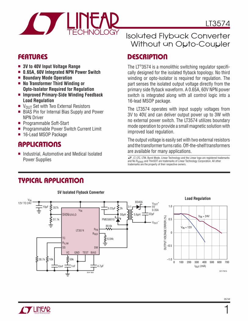
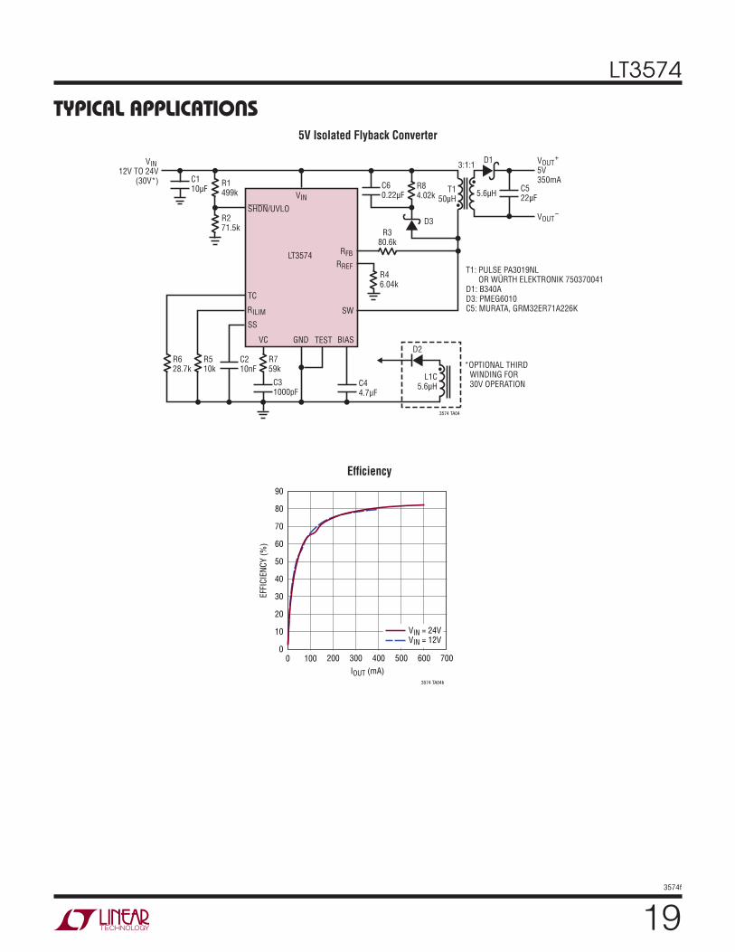
Isolated Flyback ConverterWithout an Opto-Coupler
The LT®3574 is a monolithic switching regulator specifi-cally designed for the isolated flyback topology. No third winding or opto-isolator is required for regulation. The part senses the isolated output voltage directly from the primary side flyback waveform. A 0.65A, 60V NPN power switch is integrated along with all control logic into a 16-lead MSOP package.
The LT3574 operates with input supply voltages from 3V to 40V, and can deliver output power up to 3W with no external power switch. The LT3574 utilizes boundary mode operation to provide a small magnetic solution with improved load regulation.
The output voltage is easily set with two external resistors and the transformer turns ratio. Off-the-shelf transformers are available for many applications.
5V Isolated Flyback Converter
n 3V to 40V Input Voltage Rangen 0.65A, 60V Integrated NPN Power Switchn Boundary Mode Operationn No Transformer Third Winding or
Opto-Isolator Required for Regulationn Improved Primary-Side Winding Feedback
Load Regulationn VOUT Set with Two External Resistorsn BIAS Pin for Internal Bias Supply and Power
NPN Drivern Programmable Soft-Start n Programmable Power Switch Current Limit n 16-Lead MSOP Package
n Industrial, Automotive and Medical Isolated Power Supplies
Load Regulation
SHDN/UVLO
TC
RILIM
SS
RFBRREF
SW
VC GND TEST BIAS
LT3574
3574 TA01
28.7k 10k 59k
VIN12V TO 24V VOUT
+
5V0.35A
VOUT–
VIN
3:1357k
51.1k
10µF
5.6µH50µH
•
•22µF
10nF 1nF 4.7µF
6.04k
2k
80.6k
B340A
PMEG6010
0.22µF
IOUT (mA)0
–1.0
OUTP
UT V
OLTA
GE E
RROR
(%)
–0.5
0
0.5
1.0
100 200 300 400
3574 TA01b
500 600 700
VIN = 24V
VIN = 12V
typical application
L, LT, LTC, LTM, Burst Mode, Linear Technology and the Linear logo are registered trademarks and No RSENSE and ThinSOT are trademarks of Linear Technology Corporation. All other trademarks are the property of their respective owners.

LT3574
�3574f
absolute MaxiMuM ratingsSW ............................................................................60VVIN, SHDN/UVLO, RFB, BIAS .....................................40VSS, VC, TC, RREF, RILIM ...............................................5VMaximum Junction Temperature .......................... 125°COperating Junction Temperature Range (Note 2) .................................................. –40°C to 125°CStorage Temperature Range ..................–65°C to 150°C
orDer inForMation
electrical characteristics The l denotes the specifications which apply over the full operating temperature range, otherwise specifications are at TA = 25°C. VIN = 12V, unless otherwise noted.
LEAD FREE FINISH TAPE AND REEL PART MARKING* PACKAGE DESCRIPTION TEMPERATURE RANGE
LT3574EMS#PBF LT3574EMS#TRPBF 3574 16-Lead Plastic MSOP –40°C to 125°C
LT3574IMS#PBF LT3574IMS#TRPBF 3574 16-Lead Plastic MSOP –40°C to 125°C
Consult LTC Marketing for parts specified with wider operating temperature ranges. *The temperature grade is identified by a label on the shipping container.For more information on lead free part marking, go to: http://www.linear.com/leadfree/ For more information on tape and reel specifications, go to: http://www.linear.com/tapeandreel/
PARAMETER CONDITIONS MIN TYP MAX UNITS
Input Voltage Range l 3 40 V
Quiescent Current SS = 0V VSHDN/UVLO = 0V
3.5 0
1
mA µA
Soft-Start Current SS = 0.4V 7 µA
SHDN/UVLO Pin Threshold UVLO Pin Voltage Rising l 1.15 1.22 1.29 V
SHDN/UVLO Pin Hysteresis Current VUVLO = 1V 2 2.5 3 µA
Soft-Start Threshold 0.7 V
Maximum Switching Frequency 1000 kHz
Switch Current Limit RILIM = 10k 0.65 0.9 1.1 A
Minimum Current Limit VC = 0V 100 mA
Switch VCESAT ISW = 0.5A 150 250 mV
RREF Voltage VIN = 3V
l
1.21 1.20
1.23 1.25 1.25
V
RREF Voltage Line Regulation 3V < VIN < 40V 0.01 0.03 %/ V
RREF Pin Bias Current (Note 3) l 100 600 nA
IREF Reference Current Measured at RFB Pin with RREF = 6.49k 190 µA
Error Amplifier Voltage Gain VIN = 3V 150 V/V
pin conFiguration
12345678
GNDTESTGNDSWVIN
BIASSHDN/UVLO
GND
161514131211109
GNDTCRREFRFBVCRILIMSSGND
TOP VIEW
MS PACKAGE16-LEAD PLASTIC MSOP
TJMAX = 125°C, θJA = 120°C/W, θJC = 21°C/W

LT3574
�3574f
Note 1: Stresses beyond those listed under Absolute Maximum Ratings may cause permanent damage to the device. Exposure to any Absolute Maximum Rating condition for extended periods may affect device reliability and lifetime.Note 2: The LT3574E is guaranteed to meet performance specifications from 0°C to 125°C junction temperature. Specifications over the –40°C
to 125°C operating junction temperature range are assured by design characterization and correlation with statistical process controls. The LT3574I is guaranteed over the full –40°C to 125°C operating junction temperature range.Note 3: Current flows out of the RREF pin.
electrical characteristics The l denotes the specifications which apply over the full operating temperature range, otherwise specifications are at TA = 25°C. VIN = 12V, unless otherwise noted.
typical perForMance characteristics
Output Voltage Quiescent Current Bias Pin Voltage
TA = 25°C, unless otherwise noted.
TEMPERATURE (°C)–50
4.80
V OUT
(V)
4.85
4.95
5.00
5.05
5.20
5.15
0 50 75
4.90
5.10
–25 25 100 125
3574 G01
TEMPERATURE (°C)–50
QUIE
SCEN
T CU
RREN
T (m
A)
4
5
6
25 75
3574 G02
3
2
–25 0 50 100 125
1
0
VIN = 40VBIAS = 20V
VIN = 5VBIAS = 5V
TEMPERATURE (°C)–50
2.0
BIAS
VOL
TAGE
(V)
2.4
2.6
2.8
3.2
0 50 75
2.2
3.0
–25 25 100 125
3574 G03
VIN = 40V
VIN = 12V
PARAMETER CONDITIONS MIN TYP MAX UNITS
Error Amplifier Transconductance DI = 10µA, VIN = 3V 150 µmhos
Minimum Switching Frequency VC = 0.35V 40 kHz
TC Current into RREF RTC = 20.1k 27.5 µA
BIAS Pin Voltage IBIAS = 30mA 2.9 3 3.1 V

LT3574
�3574f
typical perForMance characteristics
Switch Saturation Voltage Switch Current Limit Switch Current Limit vs RILIM
SHDN/UVLO Falling Threshold SS Pin Current
TA = 25°C, unless otherwise noted.
SWITCH CURRENT (mA)0
0
SWIT
CH V
CESA
T VO
LTAG
E (m
V)
50
150
200
250
200 400 500 900
3574 G04
100
100 300 600 700 800
300
125°C –50°C
25°C
TEMPERATURE (°C)–50
CURR
ENT
LIM
IT (m
A)
800
1000
1200
25 75
3574 G05
600
400
–25 0 50 100 125
200
0
MAXIMUM CURRENT LIMIT
MINIMUM CURRENT LIMIT
RILIM = 10k
TEMPERATURE (°C)–60
SHDN
/UVL
O VO
LTAG
E (V
)
1.24
1.26
80
1.22
–20 20–40 1200 40 10060 140
1.20
1.18
1.28
3574 G07
RILIM RESISTANCE (kΩ)1
0
SWIT
CH C
URRE
NT L
IMIT
(A)
0.2
0.4
0.6
0.8
1.0
1.2
10 20 30 40
3574 G06
50
TEMPERATURE (°C)–60
SS P
IN C
URRE
NT (µ
A)
8
10
80
6
4
–20 20–40 1200 40 10060 140
2
0
12
3574 G08

LT3574
�3574f
pin FunctionsBIAS: Bias Voltage. This pin supplies current to the switch driver and internal circuitry of the LT3574. This pin must be locally bypassed with a capacitor. This pin may also be connected to VIN if a third winding is not used and if VIN ≤ 15V. If a third winding is used, the BIAS voltage should be lower than the input voltage for proper operation.
GND: Ground.
RFB: Input Pin for External Feedback Resistor. This pin is connected to the transformer primary (VSW). The ratio of this resistor to the RREF resistor, times the internal bandgap reference, determines the output voltage (plus the effect of any non-unity transformer turns ratio). The average current through this resistor during the flyback period should be approximately 200µA. For nonisolated applications, this pin should be connected to VIN.
RILIM: Maximum Current Limit Adjust Pin. A resistor should be tied to this pin to ground to set the current limit. Use a 10k resistor for the full current capabilities of the switch.
RREF: Input Pin for External Ground-Referred Reference Resistor. This resistor should be in the range of 6k, but for convenience, need not be precisely this value. For nonisolated applications, a traditional resistor voltage divider may be connected to this pin.
SHDN/UVLO: Shutdown/Undervoltage Lockout. A resistor divider connected to VIN is tied to this pin to program the minimum input voltage at which the LT3574 will operate. At a voltage below ~0.7V, the part draws no quiescent current. When below 1.22V and above ~0.7V, the part will draw 10µA of current, but internal circuitry will remain off. Above 1.22V, the internal circuitry will start and a 7µA current will be fed into the SS pin. When this pin falls below 1.22V, 2.5µA will be pulled from the pin to provide programmable hysteresis for UVLO.
SS: Soft-Start Pin. Place a soft-start capacitor here to limit start-up inrush current and output voltage ramp rate. Switching starts when the voltage at this pin reaches ~0.7V.
SW: Collector Node of the Output Switch. This pin has large currents flowing through it. Keep the traces to the switching components as short as possible to minimize electromagnetic radiation and voltage spikes.
TC: Output Voltage Temperature Compensation. Connect a resistor to ground to produce a current proportional to absolute temperature to be sourced into the RREF node. ITC = 0.55V/RTC.
TEST: This pin is used for testing purposes only and must be connected to ground for the part to operate properly.
VC: Compensation Pin for Internal Error Amplifier. Connect a series RC from this pin to ground to compensate the switching regulator. A 100pF capacitor in parallel helps eliminate noise.
VIN: Input Voltage. This pin supplies current to the internal start-up circuitry and as a reference voltage for the DCM comparator and feedback circuitry. This pin must be locally bypassed with a capacitor.
LT3574
�3574f
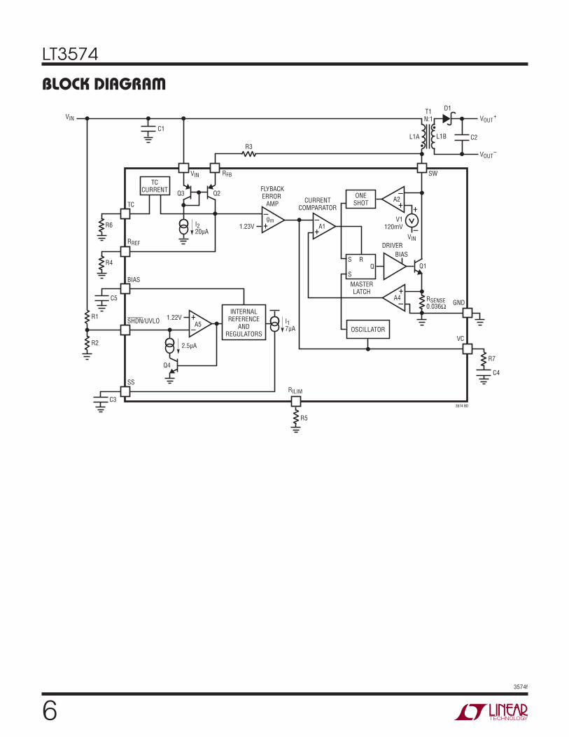
block DiagraM
FLYBACKERROR
AMP
MASTERLATCH
CURRENTCOMPARATOR
BIAS
R1
R2
C3
R6
VOUT+
VOUT–
VIN
TC
BIAS
SS
SWVIN
VIN
GND
V1120mV1.23V
VC
D1T1N:1
I17µA
I220µA
RSENSE0.036Ω
C2C1
L1A•
•L1B
R3
R4
C5
+–
OSCILLATOR
TCCURRENT
ONESHOT
RQ
S
S
gm
+–
A1
+–
A5
+–
+–
A2
A4
2.5µA
+
–
3574 BD
Q2
R7
C4
R5
Q3
1.22V
Q4
Q1
DRIVER
SHDN/UVLO
RILIM
RFB
RREF
INTERNALREFERENCE
ANDREGULATORS
LT3574
�3574f
operationThe LT3574 is a current mode switching regulator IC designed specifically for the isolated flyback topology. The special problem normally encountered in such cir-cuits is that information relating to the output voltage on the isolated secondary side of the transformer must be communicated to the primary side in order to maintain regulation. Historically, this has been done with opto-isola-tors or extra transformer windings. Opto-isolator circuits waste output power and the extra components increase the cost and physical size of the power supply. Opto-isolators can also exhibit trouble due to limited dynamic response, nonlinearity, unit-to-unit variation and aging over life. Circuits employing extra transformer windings also exhibit deficiencies. Using an extra winding adds to the transformer’s physical size and cost, and dynamic response is often mediocre.
The LT3574 derives its information about the isolated output voltage by examining the primary side flyback pulse waveform. In this manner, no opto-isolator nor extra transformer winding is required for regulation. The output voltage is easily programmed with two resistors. Since this IC operates in boundary control mode, the output voltage is calculated from the switch pin when the secondary cur-rent is almost zero. This method improves load regulation without external resistors and capacitors.
The Block Diagram shows an overall view of the system. Many of the blocks are similar to those found in traditional switching regulators including: internal bias regulator, oscillator, logic, current amplifier and comparator, driver, and output switch. The novel sections include a special flyback error amplifier and a temperature compensation circuit. In addition, the logic system contains additional logic for boundary mode operation, and the sampling error amplifier.
The LT3574 features a boundary mode control method, where the part operates at the boundary between continu-ous conduction mode and discontinuous conduction mode. The VC pin controls the current level just as it does in normal current mode operation, but instead of turning the switch on at the start of the oscillator period, the part detects when the secondary-side winding current is zero.
Boundary Mode Operation
Boundary mode is a variable frequency, current mode switching scheme. The switch turns on and the inductor current increases until a VC pin controlled current limit. The voltage on the SW pin rises to the output voltage divided by the secondary-to-primary transformer turns ratio plus the input voltage. When the secondary current through the diode falls to zero, the SW pin voltage falls below VIN. A discontinuous conduction mode (DCM) comparator detects this event and turns the switch back on.
Boundary mode returns the secondary current to zero every cycle, so the parasitic resistive voltage drops do not cause load regulation errors. Boundary mode also allows the use of a smaller transformer compared to continuous conduction mode and no subharmonic oscillation.
At low output currents the LT3574 delays turning on the switch, and thus operates in discontinuous mode. Unlike a traditional flyback converter, the switch has to turn on to update the output voltage information. Below 0.6V on the VC pin, the current comparator level decreases to its minimum value, and the internal oscillator frequency decreases in frequency. With the decrease of the internal oscillator, the part starts to operate in DCM. The output current is able to decrease while still allowing a minimum switch off-time for the error amp sampling circuitry. The typical minimum internal oscillator frequency with VC equal to 0V is 40kHz.
LT3574
�3574f
ERROR AMPLIFIER—PSEUDO DC THEORY
In the Block Diagram, the RREF (R4) and RFB (R3) resistors can be found. They are external resistors used to program the output voltage. The LT3574 operates much the same way as traditional current mode switchers, the major difference being a different type of error amplifier which derives its feedback information from the flyback pulse.
Operation is as follows: when the output switch, Q1, turns off, its collector voltage rises above the VIN rail. The am-plitude of this flyback pulse, i.e., the difference between it and VIN, is given as:
VFLBK = (VOUT + VF + ISEC • ESR) • NPS
VF = D1 forward voltage
ISEC = Transformer secondary current
ESR = Total impedance of secondary circuit
NPS = Transformer effective primary-to-secondary turns ratio
The flyback voltage is then converted to a current by the action of RFB and Q2. Nearly all of this current flows through resistor RREF to form a ground-referred voltage. This voltage is fed into the flyback error amplifier. The flyback error amplifier samples this output voltage infor-mation when the secondary side winding current is zero. The error amplifier uses a bandgap voltage, 1.23V, as the reference voltage.
The relatively high gain in the overall loop will then cause the voltage at the RREF resistor to be nearly equal to the bandgap reference voltage VBG. The relationship between VFLBK and VBG may then be expressed as:
aVR
VR
or
V VR
R
FLBK
FB
BG
REF
FLBK BGFB
REF
=
=
,
1a
a = Ratio of Q1 IC to IE, typically ≈0.986
VBG = Internal bandgap reference
applications inForMationIn combination with the previous VFLBK expression yields an expression for VOUT, in terms of the internal reference, programming resistors, transformer turns ratio and diode forward voltage drop:
V V
RR N
V I ESOUT BGFB
REF PSF SEC=
− −
1a
( RR)
Additionally, it includes the effect of nonzero secondary output impedance (ESR). This term can be assumed to be zero in boundary control mode. More details will be discussed in the next section.
Temperature Compensation
The first term in the VOUT equation does not have a tem-perature dependence, but the diode forward drop has a significant negative temperature coefficient. To compen-sate for this, a positive temperature coefficient current source is connected to the RREF pin. The current is set by a resistor to ground connected to the TC pin. To cancel the temperature coefficient, the following equation is used:
dd
dd
d
VT
RR N
VT
or
RR
N V
F FB
TC PS
TC
TCFB
PS
= −
=−
• • ,
•
1
1
FF
TC FB
PSTVT
RN/
•d
dd
≈
(dVF/dT) = Diode’s forward voltage temperature coefficient
(dVTC/dT) = 2mV
VTC = 0.55V
The resistor value given by this equation should also be verified experimentally, and adjusted if necessary to achieve optimal regulation over temperature.
The revised output voltage is as follows:
V VR
R NV
VR
OUT BGFB
REF PSF
TC
TC
=
−
−
1a
• – ( )
RN
I ESRFB
PSSECa

LT3574
�3574f
applications inForMationERROR AMPLIFIER—DYNAMIC THEORY
Due to the sampling nature of the feedback loop, there are several timing signals and other constraints that are required for proper LT3574 operation.
Minimum Current Limit
The LT3574 obtains output voltage information from the SW pin when the secondary winding conducts current. The sampling circuitry needs a minimum amount of time to sample the output voltage. To guarantee enough time, a minimum inductance value must be maintained. The primary side magnetizing inductance must be chosen above the following value:
L V
tI
N V NµHVPRI OUT
MIN
MINPS OUT PS≥ =
• • • •2
tMIN = minimum off-time, 350ns
IMIN = minimum current limit, 175mA
The minimum current limit is higher than that on the Elec-trical Characteristics table due to the overshoot caused by the comparator delay.
Leakage Inductance Blanking
When the output switch first turns off, the flyback pulse appears. However, it takes a finite time until the transformer primary-side voltage waveform approximately represents the output voltage. This is partly due to the rise time on the SW node, but more importantly due to the trans- former leakage inductance. The latter causes a very fast voltage spike on the primary side of the transformer that is not directly related to output voltage (some time is also required for internal settling of the feedback amplifier circuitry). The leakage inductance spike is largest when the power switch current is highest.
In order to maintain immunity to these phenomena, a fixed delay is introduced between the switch turn-off command and the beginning of the sampling. The blanking is internally set to 150ns. In certain cases, the leakage inductance may not be settled by the end of the blanking period, but will not significantly affect output regulation.
Selecting RFB and RREF Resistor Values
The expression for VOUT, developed in the Operation sec-tion, can be rearranged to yield the following expression for RFB:
R
R N V V V
VFBREF PS OUT F TC
BG=
+( ) + • a
where,
VOUT = Output voltage VF = Switching diode forward voltage a = Ratio of Q1, IC to IE, typically 0.986 NPS = Effective primary-to-secondary turns ratio VTC = 0.55V
The equation assumes the temperature coefficients of the diode and VTC are equal, which is a good first-order approximation.
Strictly speaking, the above equation defines RFB not as an absolute value, but as a ratio of RREF. So, the next ques-tion is, “What is the proper value for RREF?” The answer is that RREF should be approximately 6.04k. The LT3574 is trimmed and specified using this value of RREF. If the impedance of RREF varies considerably from 6.04k, ad-ditional errors will result. However, a variation in RREF of several percent is acceptable. This yields a bit of freedom in selecting standard 1% resistor values to yield nominal RFB/RREF ratios. The RFB resistor given by this equation should also be verified experimentally, and adjusted if necessary for best output accuracy.
Tables 1-4 are useful for selecting the resistor values for RREF and RFB with no equations. The tables provide RFB, RREF and RTC values for common output voltages and common winding ratios. Table 1. Common Resistor Values for 1:1 Transformers
VOUT (V) NPS RFB (kΩ) RREF (kΩ) RTC (kΩ)
3.3 1.00 18.7 6.04 19.1
5 1.00 27.4 6.04 28
12 1.00 64.9 6.04 66.5
15 1.00 80.6 6.04 80.6
20 1.00 107 6.04 105
LT3574
�03574f
Table 2. Common Resistor Values for 2:1 TransformersVOUT (V) NPS RFB (kΩ) RREF (kΩ) RTC (kΩ)
3.3 2.00 37.4 6.04 18.7
5 2.00 56 6.04 28
12 2.00 130 6.04 66.5
15 2.00 162 6.04 80.6
Table 3. Common Resistor Values for 3:1 Transformers
VOUT (V) NPS RFB (kΩ) RREF (kΩ) RTC (kΩ)
3.3 3.00 56.2 6.04 20
5 3.00 80.6 6.04 28.7
10 3.00 165 6.04 54.9
Table 4. Common Resistor Values for 4:1 Transformers
VOUT (V) NPS RFB (kΩ) RREF (kΩ) RTC (kΩ)
3.3 4.00 76.8 6.04 19.1
5 4.00 113 6.04 28
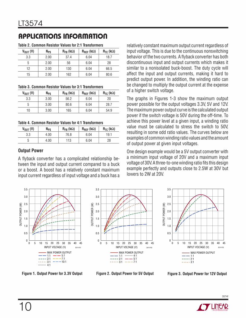
Output Power
A flyback converter has a complicated relationship be-tween the input and output current compared to a buck or a boost. A boost has a relatively constant maximum input current regardless of input voltage and a buck has a
relatively constant maximum output current regardless of input voltage. This is due to the continuous nonswitching behavior of the two currents. A flyback converter has both discontinuous input and output currents which makes it similar to a nonisolated buck-boost. The duty cycle will affect the input and output currents, making it hard to predict output power. In addition, the winding ratio can be changed to multiply the output current at the expense of a higher switch voltage.
The graphs in Figures 1-3 show the maximum output power possible for the output voltages 3.3V, 5V and 12V. The maximum power output curve is the calculated output power if the switch voltage is 50V during the off-time. To achieve this power level at a given input, a winding ratio value must be calculated to stress the switch to 50V, resulting in some odd ratio values. The curves below are examples of common winding ratio values and the amount of output power at given input voltages.
One design example would be a 5V output converter with a minimum input voltage of 20V and a maximum input voltage of 30V. A three-to-one winding ratio fits this design example perfectly and outputs close to 2.5W at 30V but lowers to 2W at 20V.
Figure 1. Output Power for 3.3V Output Figure 2. Output Power for 5V Output Figure 3. Output Power for 12V Output
INPUT VOLTAGE (V)0
OUTP
UT P
OWER
(W)
1.5
2.0
2.5
403574 F01
1.0
0.5
010 20 305 4515 25 35
3.5
3.0
MAX POWER OUTPUT1:12:13:14:1
5:17:110:1
INPUT VOLTAGE (V)0
OUTP
UT P
OWER
(W)
1.5
2.0
2.5
403574 F02
1.0
0.5
010 20 305 4515 25 35
3.5
3.0
MAX POWER OUTPUT1:12:13:1
4:15:17:1
INPUT VOLTAGE (V)0
OUTP
UT P
OWER
(W)
1.5
2.0
2.5
403574 F03
1.0
0.5
010 20 305 4515 25 35
3.5
3.0
MAX POWER OUTPUT1:12:13:1
applications inForMation

LT3574
��3574f
TRANSFORMER DESIGN CONSIDERATIONS
Transformer specification and design is perhaps the most critical part of successfully applying the LT3574. In addition to the usual list of caveats dealing with high frequency isolated power supply transformer design, the following information should be carefully considered.
Linear Technology has worked with several leading mag-netic component manufacturers to produce pre-designed flyback transformers for use with the LT3574. Table 5 shows the details of several of these transformers.
applications inForMation
Table 5. Predesigned Transformers—Typical Specifications Unless Otherwise NotedTRANSFORMER PART NUMBER
SIZE (W × L × H) mm
LPRI (µH)
LLEAKAGE (nH) NP:NS:NB
RPRI (mΩ)
RSEC (mΩ) VENDOR
TARGET APPLICATIONS
PA3018NL 12.70 × 10.67 × 9.14 50 700 4:1:1 250 32 Pulse Engineering 3.3V, 0.7A
PA2626NL 12.70 × 10.67 × 9.14 30 403 3:1:1 240 66 Pulse Engineering 5V, 0.5A
PA2627NL 15.24 × 13.1 × 11.45 50 766 3:1:1 420 44 Pulse Engineering 5V, 0.5A
PA3019NL 12.70 × 10.67 × 9.14 50 700 3:1:1 250 72 Pulse Engineering 5V, 0.5A
PA3020NL 12.70 × 10.67 × 9.14 60 680 2:1:0.33 400 200 Pulse Engineering 12V, 0.25A
PA3021NL 12.70 × 10.67 × 9.14 50 195 1:1:0.33 100 200 Pulse Engineering 15V, 0.15A
750311304 15.24 × 13.3 × 11.43 50 825 4:1:1.5 146 17 Würth Elektronik 3.3V, 0.7A
750310564 15.24 × 13.3 × 11.43 63 450 3:1:1 115 50 Würth Elektronik ±5V, 0.5A
750370040 9.14 × 9.78 × 10.54 30 150 3:1:1 60 12.5 Würth Elektronik 5V, 0.5A
750370041 9.14 × 9.78 × 10.54 50 450 3:1:1 190 26 Würth Elektronik 5V, 0.5A
750370047 13.35 × 10.8 × 9.14 30 150 3:1:1 60 12.5 Würth Elektronik 5V, 0.5A
750311307 15.24 × 13.3 × 11.43 100 2000 2:1:0.33 173 104 Würth Elektronik 12V, 0.25A
750311308 15.24 × 13.3 × 11.43 100 2090 1:1:0.33 325 480 Würth Elektronik 15V, 0.15A
L10-1022 9.52 × 9.52 × 4.95 30 - 1:1 0.142 0.142 BH Electronics 5V, 0.1A
LT3574
��3574f
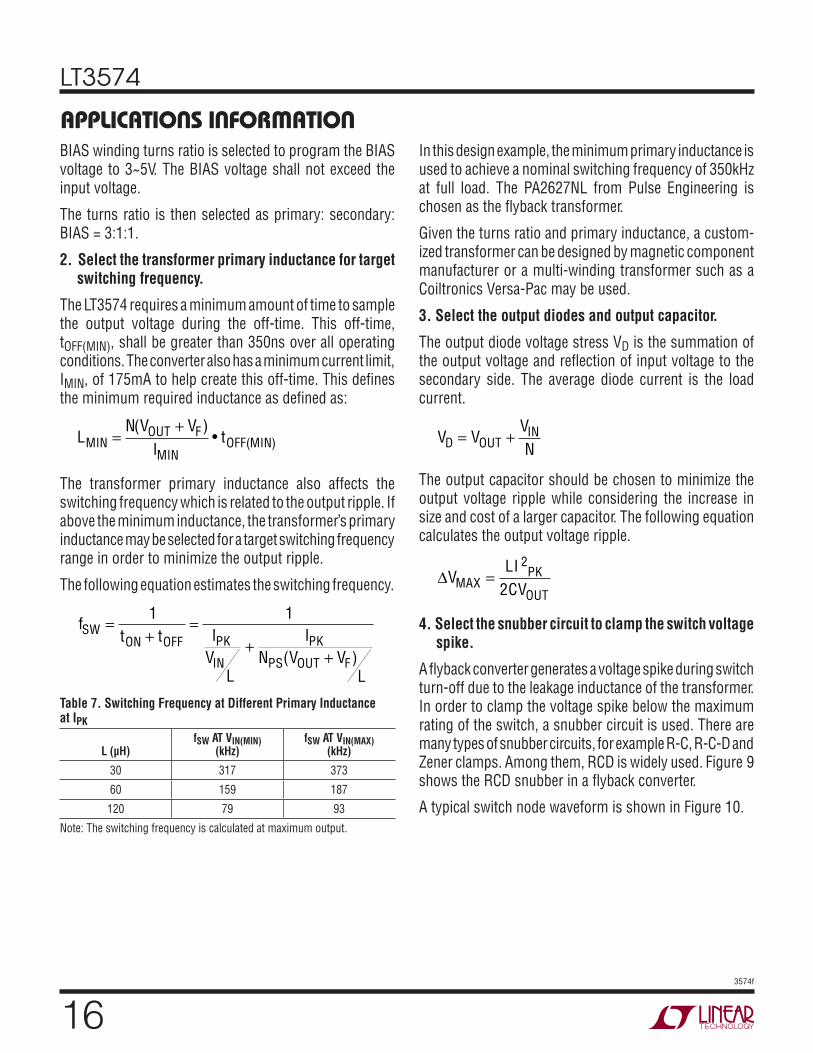
applications inForMationTurns Ratio
Note that when using an RFB/RREF resistor ratio to set output voltage, the user has relative freedom in selecting a transformer turns ratio to suit a given application. In contrast, simpler ratios of small integers, e.g., 1:1, 2:1, 3:2, etc., can be employed to provide more freedom in setting total turns and mutual inductance.
Typically, the transformer turns ratio is chosen to maximize available output power. For low output voltages (3.3V or 5V), a N:1 turns ratio can be used with multiple primary windings relative to the secondary to maximize the transformer’s current gain (and output power). However, remember that the SW pin sees a voltage that is equal to the maximum input supply voltage plus the output voltage multiplied by the turns ratio. This quantity needs to remain below the abs max rating of the SW pin to prevent breakdown of the internal power switch. Together these conditions place an upper limit on the turns ratio, N, for a given application. Choose a turns ratio low enough to ensure:
N
V V
V VIN MAX
OUT F<
+50 – ( )
For larger N:1 values, a transformer with a larger physical size is needed to deliver additional current and provide a large enough inductance value to ensure that the off-time is long enough to accurately measure the output voltage.
For lower output power levels, a 1:1 or 1:N transformer can be chosen for the absolute smallest transformer size. A 1:N transformer will minimize the magnetizing induc-tance (and minimize size), but will also limit the available output power. A higher 1:N turns ratio makes it possible to have very high output voltages without exceeding the breakdown voltage of the internal power switch.
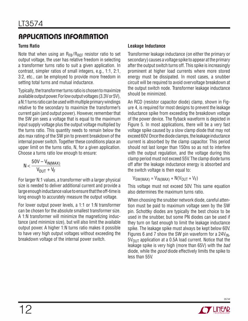
Leakage Inductance
Transformer leakage inductance (on either the primary or secondary) causes a voltage spike to appear at the primary after the output switch turns off. This spike is increasingly prominent at higher load currents where more stored energy must be dissipated. In most cases, a snubber circuit will be required to avoid overvoltage breakdown at the output switch node. Transformer leakage inductance should be minimized.
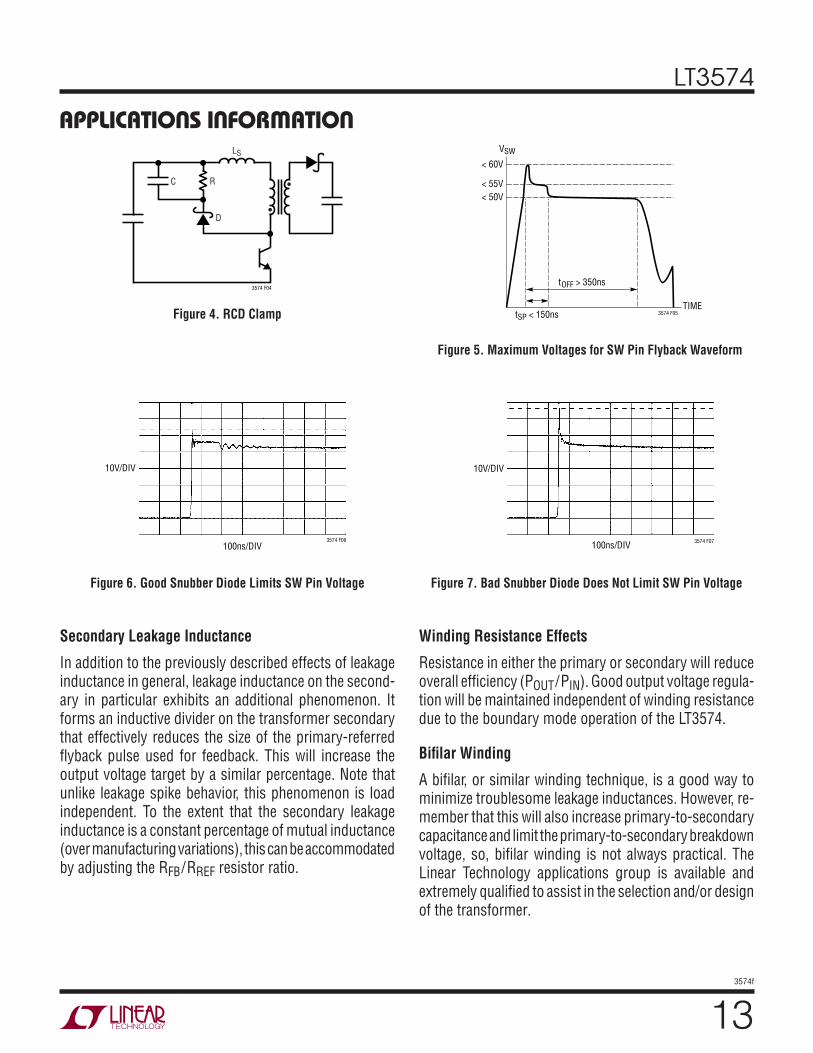
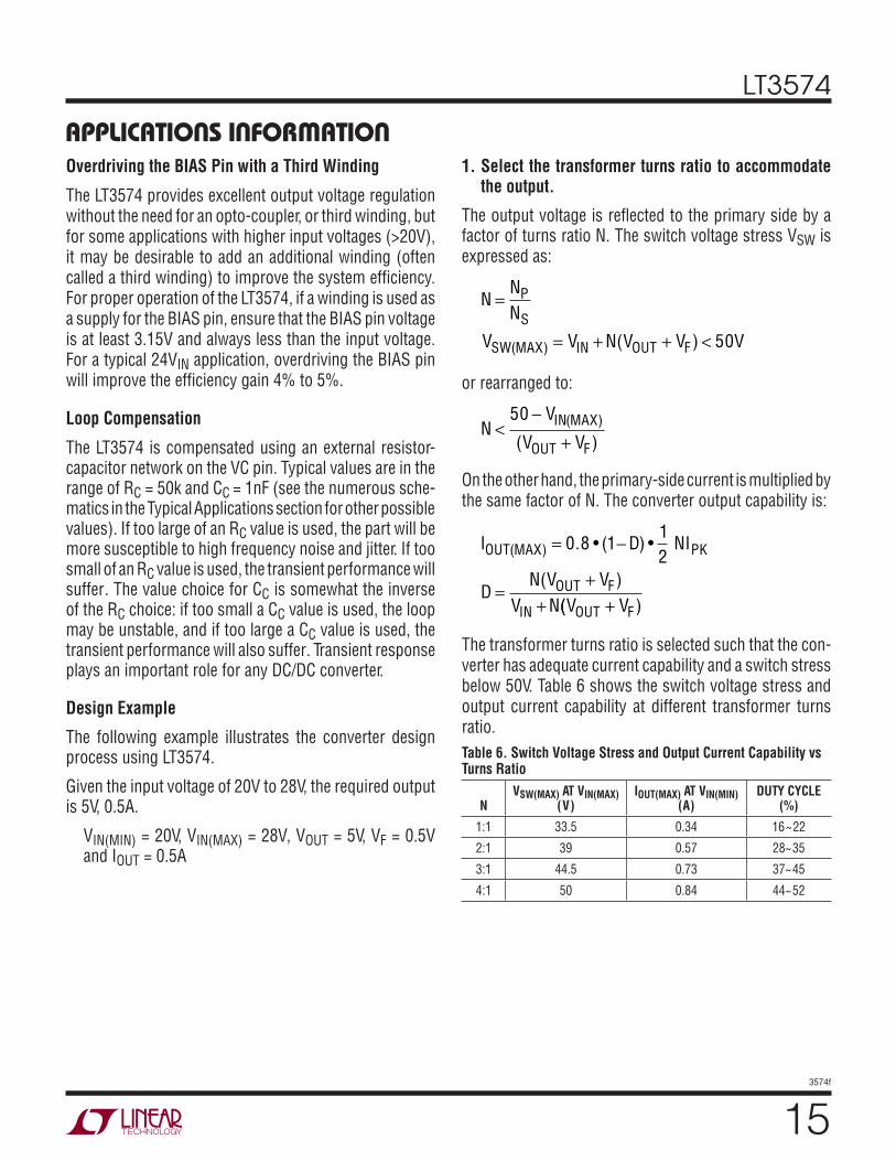
An RCD (resistor capacitor diode) clamp, shown in Fig-ure 4, is required for most designs to prevent the leakage inductance spike from exceeding the breakdown voltage of the power device. The flyback waveform is depicted in Figure 5. In most applications, there will be a very fast voltage spike caused by a slow clamp diode that may not exceed 60V. Once the diode clamps, the leakage inductance current is absorbed by the clamp capacitor. This period should not last longer than 150ns so as not to interfere with the output regulation, and the voltage during this clamp period must not exceed 55V. The clamp diode turns off after the leakage inductance energy is absorbed and the switch voltage is then equal to:
VSW(MAX) = VIN(MAX) + N(VOUT + VF)
This voltage must not exceed 50V. This same equation also determines the maximum turns ratio.
When choosing the snubber network diode, careful atten-tion must be paid to maximum voltage seen by the SW pin. Schottky diodes are typically the best choice to be used in the snubber, but some PN diodes can be used if they turn on fast enough to limit the leakage inductance spike. The leakage spike must always be kept below 60V. Figures 6 and 7 show the SW pin waveform for a 24VIN, 5VOUT application at a 0.5A load current. Notice that the leakage spike is very high (more than 65V) with the bad diode, while the good diode effectively limits the spike to less than 55V.
LT3574
��3574f
applications inForMation
Figure 5. Maximum Voltages for SW Pin Flyback Waveform
Figure 4. RCD Clamp
Figure 6. Good Snubber Diode Limits SW Pin Voltage Figure 7. Bad Snubber Diode Does Not Limit SW Pin Voltage
< 50V< 55V
< 60V
VSW
tOFF > 350ns
TIMEtSP < 150ns 3574 F05
100ns/DIV
10V/DIV
3574 F06100ns/DIV
10V/DIV
3574 F07
3574 F04
LS
D•
RC •
Secondary Leakage Inductance
In addition to the previously described effects of leakage inductance in general, leakage inductance on the second-ary in particular exhibits an additional phenomenon. It forms an inductive divider on the transformer secondary that effectively reduces the size of the primary-referred flyback pulse used for feedback. This will increase the output voltage target by a similar percentage. Note that unlike leakage spike behavior, this phenomenon is load independent. To the extent that the secondary leakage inductance is a constant percentage of mutual inductance (over manufacturing variations), this can be accommodated by adjusting the RFB/RREF resistor ratio.
Winding Resistance Effects
Resistance in either the primary or secondary will reduce overall efficiency (POUT/PIN). Good output voltage regula-tion will be maintained independent of winding resistance due to the boundary mode operation of the LT3574.
Bifilar Winding
A bifilar, or similar winding technique, is a good way to minimize troublesome leakage inductances. However, re-member that this will also increase primary-to-secondary capacitance and limit the primary-to-secondary breakdown voltage, so, bifilar winding is not always practical. The Linear Technology applications group is available and extremely qualified to assist in the selection and/or design of the transformer.

LT3574
��3574f
applications inForMationSetting the Current Limit Resistor
The maximum current limit can be set by placing a resistor between the RILIM pin and ground. This provides some flexibility in picking standard off-the-shelf transformers that may be rated for less current than the LT3574’s internal power switch current limit. If the maximum current limit is needed, use a 10k resistor. For lower current limits, the following equation sets the approximate current limit:
R A I kILIM LIM= − +65 10 0 9 103• ( . )
The Switch Current Limit vs RILIM plot in the Typical Per-formance Characteristics section depicts a more accurate current limit.
Undervoltage Lockout (UVLO)
The SHDN/UVLO pin is connected to a resistive voltage divider connected to VIN as shown in Figure 8. The voltage threshold on the SHDN/UVLO pin for VIN rising is 1.22V. To introduce hysteresis, the LT3574 draws 2.5µA from the SHDN/UVLO pin when the pin is below 1.22V. The hysteresis is therefore user-adjustable and depends on the value of R1. The UVLO threshold for VIN rising is:
V
V R RR
µA RIN UVLO RISING( , ). • ( )
. •=+
+1 22 1 2
22 5 1
The UVLO threshold for VIN falling is:
V
V R RRIN UVLO FALLING( , )
. • ( )=
+1 22 1 22
To implement external run/stop control, connect a small NMOS to the UVLO pin, as shown in Figure 8. Turning the NMOS on grounds the UVLO pin and prevents the LT3574 from operating, and the part will draw less than a 1µA of quiescent current.
Minimum Load Requirement
The LT3574 obtains output voltage information through the transformer while the secondary winding is conducting current. During this time, the output voltage (multiplied times the turns ratio) is presented to the primary side of the transformer. The LT3574 uses this reflected signal to regulate the output voltage. This means that the LT3574 must turn on every so often to sample the output voltage, which delivers a small amount of energy to the output. This sampling places a minimum load requirement on the output of 1% to 2% of the maximum load.
BIAS Pin Considerations
For applications with an input voltage less than 15V, the BIAS pin is typically connected directly to the VIN pin. For input voltages greater than 15V, it is preferred to leave the BIAS pin separate from the VIN pin. In this condition, the BIAS pin is regulated with an internal LDO to a voltage of 3V. By keeping the BIAS pin separate from the input voltage at high input voltages, the physical size of the capacitors can be minimized (the BIAS pin can then use a 6.3V or 10V rated capacitor).
Figure 8. Undervoltage Lockout (UVLO)
LT3574
SHDN/UVLO
GND
R2
R1
VIN
3574 F08
RUN/STOPCONTROL(OPTIONAL)
LT3574
��3574f
applications inForMationOverdriving the BIAS Pin with a Third Winding
The LT3574 provides excellent output voltage regulation without the need for an opto-coupler, or third winding, but for some applications with higher input voltages (>20V), it may be desirable to add an additional winding (often called a third winding) to improve the system efficiency. For proper operation of the LT3574, if a winding is used as a supply for the BIAS pin, ensure that the BIAS pin voltage is at least 3.15V and always less than the input voltage. For a typical 24VIN application, overdriving the BIAS pin will improve the efficiency gain 4% to 5%.
Loop Compensation
The LT3574 is compensated using an external resistor-capacitor network on the VC pin. Typical values are in the range of RC = 50k and CC = 1nF (see the numerous sche-matics in the Typical Applications section for other possible values). If too large of an RC value is used, the part will be more susceptible to high frequency noise and jitter. If too small of an RC value is used, the transient performance will suffer. The value choice for CC is somewhat the inverse of the RC choice: if too small a CC value is used, the loop may be unstable, and if too large a CC value is used, the transient performance will also suffer. Transient response plays an important role for any DC/DC converter.
Design Example
The following example illustrates the converter design process using LT3574.
Given the input voltage of 20V to 28V, the required output is 5V, 0.5A.
VIN(MIN) = 20V, VIN(MAX) = 28V, VOUT = 5V, VF = 0.5V and IOUT = 0.5A
1. Select the transformer turns ratio to accommodate the output.
The output voltage is reflected to the primary side by a factor of turns ratio N. The switch voltage stress VSW is expressed as:
NNN
V V N V V V
P
S
SW MAX IN OUT F
=
= + + <( ) ( ) 50
or rearranged to:
N
V
V VIN MAX
OUT F<
−+
50 ( )
( )
On the other hand, the primary-side current is multiplied by the same factor of N. The converter output capability is:
I D NI
DN V V
V N
OUT MAX PK
OUT F
IN
( ) . • ( ) •
( )
= −
=+
+
0 8 112
(( )V VOUT F+
The transformer turns ratio is selected such that the con-verter has adequate current capability and a switch stress below 50V. Table 6 shows the switch voltage stress and output current capability at different transformer turns ratio.Table 6. Switch Voltage Stress and Output Current Capability vs Turns Ratio
NVSW(MAX) AT VIN(MAX)
(V)IOUT(MAX) AT VIN(MIN)
(A)DUTY CYCLE
(%)
1:1 33.5 0.34 16~22
2:1 39 0.57 28~35
3:1 44.5 0.73 37~45
4:1 50 0.84 44~52
LT3574
��3574f
applications inForMationBIAS winding turns ratio is selected to program the BIAS voltage to 3~5V. The BIAS voltage shall not exceed the input voltage.
The turns ratio is then selected as primary: secondary: BIAS = 3:1:1.
2. Select the transformer primary inductance for target switching frequency.
The LT3574 requires a minimum amount of time to sample the output voltage during the off-time. This off-time, tOFF(MIN), shall be greater than 350ns over all operating conditions. The converter also has a minimum current limit, IMIN, of 175mA to help create this off-time. This defines the minimum required inductance as defined as:
L
N V VI
tMINOUT F
MINOFF MIN=
+( )• ( )
The transformer primary inductance also affects the switching frequency which is related to the output ripple. If above the minimum inductance, the transformer’s primary inductance may be selected for a target switching frequency range in order to minimize the output ripple.
The following equation estimates the switching frequency.
ft t I
VL
IN V V
L
SWON OFF PK
IN
PK
PS OUT F
=+
=+
+
1 1
( )
Table 7. Switching Frequency at Different Primary Inductance at IPK
L (µH)fSW AT VIN(MIN)
(kHz)fSW AT VIN(MAX)
(kHz)
30 317 373
60 159 187
120 79 93
Note: The switching frequency is calculated at maximum output.
In this design example, the minimum primary inductance is used to achieve a nominal switching frequency of 350kHz at full load. The PA2627NL from Pulse Engineering is chosen as the flyback transformer.
Given the turns ratio and primary inductance, a custom-ized transformer can be designed by magnetic component manufacturer or a multi-winding transformer such as a Coiltronics Versa-Pac may be used.
3. Select the output diodes and output capacitor.
The output diode voltage stress VD is the summation of the output voltage and reflection of input voltage to the secondary side. The average diode current is the load current.
V V
VND OUTIN= +
The output capacitor should be chosen to minimize the output voltage ripple while considering the increase in size and cost of a larger capacitor. The following equation calculates the output voltage ripple.
DV
LICVMAX
PK
OUT=
2
2
4. Select the snubber circuit to clamp the switch voltage spike.
A flyback converter generates a voltage spike during switch turn-off due to the leakage inductance of the transformer. In order to clamp the voltage spike below the maximum rating of the switch, a snubber circuit is used. There are many types of snubber circuits, for example R-C, R-C-D and Zener clamps. Among them, RCD is widely used. Figure 9 shows the RCD snubber in a flyback converter.
A typical switch node waveform is shown in Figure 10.

LT3574
��3574f
applications inForMation
Figure 9. RCD Snubber in a Flyback Converter Figure 10. Typical Switch Node Waveform
3574 F09
LS
D
R
•
C •
VIN
VCNVOUT
tSP3574 F10
During switch turn-off, the energy stored in the leakage inductance is transferred to the snubber capacitor, and eventually dissipated in the snubber resistor.
12
2L I fV V N V
RS PK SWC C OUT=
−( • )
The snubber resistor affects the spike amplitude VC and duration tSP, the snubber resistor is adjusted such that tSP is about 150ns. Prolonged tSP may cause distortion to the output voltage sensing.
The previous steps finish the flyback power stage design.
5. Select the feedback resistor for proper output voltage.
Using the resistor Tables 1-4, select the feedback resis-tor RFB, and program the output voltage to 5V. Adjust the RTC resistor for temperature compensation of the output voltage. RREF is selected as 6.04k.
A small capacitor in parallel with RREF filters out the noise during the voltage spike, however, the capacitor should limit to 10pF. A large capacitor causes distortion on volt-age sensing.
6. Optimize the compensation network to improve the transient performance.
The transient performance is optimized by adjusting the compensation network. For best ripple performance, select a compensation capacitor not less than 1nF, and select a compensation resistor not greater than 50k.
7. Current limit resistor, soft-start capacitor and UVLO resistor divider
Use the current limit resistor RLIM to lower the current limit if a compact transformer design is required. Soft-start capacitor helps during the start-up of the flyback converter.Select the UVLO resistor divider for intended input opera-tion range. These equations are aforementioned.
LT3574
��3574f
±12V Isolated Flyback Converter
typical applications
SHDN/UVLO
TC
SS
SW
VC GND BIAS
LT3574
3574 TA02
R628.7k
R510k
VIN5V
VOUT+
5V175mA
VOUT–
VIN
3:1D1
VIN
R1200k
R290.9k
C110µF C5
22µFT1
30µH 3.3µH
T1: PULSE PA2626NL OR WÜRTH ELEKTRONIK 750370040D1: B340AD2: PMEG6010C5: MURATA, GRM32ER71A226K
R46.04k
R380.6k
C210nF
C31500pF
R759k
R82k
D2
C60.22µF
TEST
RILIM
RFBRREF
SHDN/UVLO
TC
SS
SW
VC GND BIAS
LT3574
3574 TA03
R659k
R510k
VIN5V
VIN
2:1:1
VIN
R1200k
R290.9k
C110µF T1
43.6µH
T1: COILTRONICS VPH1-0076-RD1, D2: B240AD3: PMEG6010C5, C6: MURATA, GRM32ER71A226K
R46.04k
R3118k
VOUT1+
12V40mA
VOUT1–
D1
•
C522µF10.9µH
VOUT2+
VOUT2–
–12V40mA
D2
C622µF10.9µH
C210nF
C30.01µF
R756.2k
R82k
D3
C60.22µF
TEST
RILIM
RFBRREF
•
Low Input Voltage 5V Isolated Flyback Converter
LT3574
��3574f
typical applications
VOUT+
5V350mA
VOUT–
D1
C522µF5.6µH
T1: PULSE PA3019NL OR WÜRTH ELEKTRONIK 750370041D1: B340AD3: PMEG6010C5: MURATA, GRM32ER71A226K
SHDN/UVLO
TC
SS
SW
VC GND BIAS
LT3574
3574 TA04
R628.7k
R510k
VIN12V TO 24V
(30V*)
VIN
3:1:1
R1499k
R271.5k
C110µF T1
50µH
R46.04k
R380.6k
C31000pF
C44.7µF
C210nF
R759k *OPTIONAL THIRD
WINDING FOR 30V OPERATION
D2
L1C5.6µH
R84.02k
D3
C60.22µF
TEST
RILIM
RFBRREF
•
•
•
5V Isolated Flyback Converter
Efficiency
IOUT (mA)0
EFFI
CIEN
CY (%
)
200 400100 300 500 600 700
3574 TA04b
60
70
80
50
40
10
0
30
90
20
VIN = 24VVIN = 12V
LT3574
�03574f
SHDN/UVLO
TC
SS
SW
VC GND BIAS
LT3574
3574 TA05
R619.1k
R510k
VIN12V TO 24V
(36V*)
VIN
4:1:1
R1499k
R271.5k
C110µF T1
50µH
T1: PULSE PA3018NL OR WÜRTH ELEKTRONIK 750311304D1: B340AD3: PMEG6010
R46.04k
R376.8k
VOUT+
3.3V0.5A
VOUT–
D1
C547µF3.1µH
C31500pF
C44.7µF
C210nF
R725.5k
*OPTIONAL THIRD WINDING FOR 36V OPERATION
D2
L1C3.1µH
R82k
D3
C60.22µF
TEST
RILIM
RFBRREF
•
•
3.3V Isolated Flyback Converter
typical applications
12V Isolated Flyback Converter
SHDN/UVLO
TC
SS SWVC GND BIAS
LT3574
3574 TA06
R659k
R510k
VIN12V
VOUT12V150mA
VOUT–
VIN
3:1D1
VIN
R1499k
R271.5k
C110µF C5
22µFT1
58.5µH 6.5µH
T1: COILTRONICS VP1-0102-RD1: B340AD2: PMEG6010
R46.04k
R3178k
C210nF
C34700pF
R740.2k
R82k
D2
C60.22µF
TEST
RILIM
RFBRREF
•
•
LT3574
��3574f
typical applications Four Output 12V Isolated Flyback Converter
SHDN/UVLO
TC
SS SWVC GND BIAS
LT3574
3574 TA07
R659k
R510k
VIN12V TO 24V
VIN
2:1:1:1:1
VIN
R1499k
R271.5k
C110µF
T143.6µH
T1: COILTRONICS VPH1-0076-RD1-D4: B240AD5: PMEG6010
R46.04k
R3118k
VOUT1+
12V40mA
VOUT1–
C522µF10.9µH
D1
C210nF
C30.1µF
R720k
R82k
D5
C60.22µF
TEST
RILIM
RFBRREF
•
•
VOUT2+
12V40mA
VOUT2–
C622µF10.9µH
D2
•
VOUT3+
12V40mA
VOUT3–
C722µF10.9µH
D3
•
VOUT4+
12V40mA
VOUT4–
C822µF10.9µH
D4
•

LT3574
��3574f
typical applications 5V Isolated Flyback Converter Using Coupling Inductor
SHDN/UVLO
TC
SS SWVC GND BIAS
LT3574
3574 TA09
R626.1k
R510k
VIN5V
VOUT+
5V0.1A
VOUT–
VIN
1:1
D1
VIN
R1200k
R290.9k
C110µF C5
47µFT1
30µH30µH
T1: BH ELECTRONICS, L10-1022D1: B220AD2: CMDSH-3
R46.04k
R326.1k
C210nF
C33300pF
R754.9k
R82k
D2
C60.22µF
TEST
RILIM
RFBRREF
•
•
LT3574
��3574f
Information furnished by Linear Technology Corporation is believed to be accurate and reliable. However, no responsibility is assumed for its use. Linear Technology Corporation makes no representa-tion that the interconnection of its circuits as described herein will not infringe on existing patent rights.
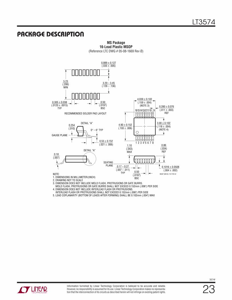
package DescriptionMS Package
16-Lead Plastic MSOP(Reference LTC DWG # 05-08-1669 Rev Ø)
MSOP (MS16) 1107 REV Ø
0.53 0.152(.021 .006)
SEATINGPLANE
0.18(.007)
1.10(.043)MAX
0.17 – 0.27(.007 – .011)
TYP
0.86(.034)REF
0.50(.0197)
BSC
16151413121110
1 2 3 4 5 6 7 8
9
NOTE:1. DIMENSIONS IN MILLIMETER/(INCH)2. DRAWING NOT TO SCALE3. DIMENSION DOES NOT INCLUDE MOLD FLASH, PROTRUSIONS OR GATE BURRS. MOLD FLASH, PROTRUSIONS OR GATE BURRS SHALL NOT EXCEED 0.152mm (.006") PER SIDE4. DIMENSION DOES NOT INCLUDE INTERLEAD FLASH OR PROTRUSIONS. INTERLEAD FLASH OR PROTRUSIONS SHALL NOT EXCEED 0.152mm (.006") PER SIDE5. LEAD COPLANARITY (BOTTOM OF LEADS AFTER FORMING) SHALL BE 0.102mm (.004") MAX
0.254(.010) 0 – 6 TYP
DETAIL “A”
DETAIL “A”
GAUGE PLANE
5.23(.206)MIN
3.20 – 3.45(.126 – .136)
0.889 0.127(.035 .005)
RECOMMENDED SOLDER PAD LAYOUT
0.305 0.038(.0120 .0015)
TYP
0.50(.0197)
BSC
4.039 0.102(.159 .004)
(NOTE 3)
0.1016 0.0508(.004 .002)
3.00 0.102(.118 .004)
(NOTE 4)
0.280 0.076(.011 .003)
REF
4.90 0.152(.193 .006)
LT3574
��3574f
Linear Technology Corporation1630 McCarthy Blvd., Milpitas, CA 95035-7417 (408) 432-1900 ● FAX: (408) 434-0507 ● www.linear.com LINEAR TECHNOLOGY CORPORATION 2010
LT 0110 • PRINTED IN USA
relateD parts
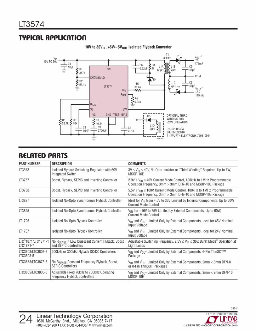
typical application10V to 30VIN, +5V/–5VOUT Isolated Flyback Converter
SHDN/UVLO
TC
SS SW
VC GND BIAS
LT3574
3574 TA11
R528.7k
R610k
VIN10V TO 30V
VIN
T13:1:1:1
R1357k
R251.1k
C110µF L1A
63µH
R46.04k
R380.6k
VOUT+
5V175mA
COM
VOUT–
–5V175mA
D1
C547µF
D2
C647µF
L1B7µH
L1C7µH
C32700pF
R740.2k
C44.7µF
C210nF
*OPTIONAL THIRD WINDING FOR >24V OPERATION
D1, D2: B340A D4: PMEG6010 T1: WÜRTH ELEKTRONIK 750310564
D3
L1D7µH
R82k
D4
•
•
•
C60.22µF
TEST
RILIM
RFBRREF
PART NUMBER DESCRIPTION COMMENTS
LT3573 Isolated Flyback Switching Regulator with 60V Integrated Switch
3V ≤ VIN ≤ 40V, No Opto-Isolator or “Third Winding” Required, Up to 7W, MSOP-16E
LT3757 Boost, Flyback, SEPIC and Inverting Controller 2.9V ≤ VIN ≤ 40V, Current Mode Control, 100kHz to 1MHz Programmable Operation Frequency, 3mm × 3mm DFN-10 and MSOP-10E Package
LT3758 Boost, Flyback, SEPIC and Inverting Controller 5.5V ≤ VIN ≤ 100V, Current Mode Control, 100kHz to 1MHz Programmable Operation Frequency, 3mm × 3mm DFN-10 and MSOP-10E Package
LT3837 Isolated No-Opto Synchronous Flyback Controller Ideal for VIN from 4.5V to 36V Limited by External Components, Up to 60W, Current Mode Control
LT3825 Isolated No-Opto Synchronous Flyback Controller VIN from 16V to 75V Limited by External Components, Up to 60W, Current Mode Control
LT1725 Isolated No-Opto Flyback Controller VIN and VOUT Limited Only by External Components, Ideal for 48V Nominal Input Voltage
LT1737 Isolated No-Opto Flyback Controller VIN and VOUT Limited Only by External Components, Ideal for 24V Nominal Input Voltage
LTC®1871/LTC1871-1 LTC1871-7
No RSENSE™ Low Quiescent Current Flyback, Boost and SEPIC Controllers
Adjustable Switching Frequency, 2.5V ≤ VIN ≤ 36V, Burst Mode® Operation at Light Loads
LTC3803/LTC3803-3 LTC3803-5
200kHz or 300kHz Flyback DC/DC Controllers VIN and VOUT Limited Only by External Components, 6-Pin ThinSOT™ Package
LTC3873/LTC3873-5 No RSENSE Constant Frequency Flyback, Boost, SEPIC Controllers
VIN and VOUT Limited Only by External Components, 2mm × 3mm DFN-8 or 8-Pin ThinSOT Packages
LTC3805/LTC3805-5 Adjustable Fixed 70kHz to 700kHz Operating Frequency Flyback Controllers
VIN and VOUT Limited Only by External Components, 3mm × 3mm DFN-10, MSOP-10E


![U-165 Reference Design: Isolated 50 Watt Flyback Converter ...Transformer Design [2] The transformer in a flyback converter is actually a coupled inductor with multiple windings. Trans-formers](https://img.pdfslide.us/doc/110x75/6067efcf513c1477013c4438/u-165-reference-design-isolated-50-watt-flyback-converter-transformer-design.jpg)