Embed Size (px)
Citation preview

By VITO KLAUDIO, in the same group as Babich Alex and Ferley Taras
LPM REGISTER
LPM REGISTER
1 October 28, 2015
Table of contents
1. Objective .................................................................................... pg. 2
2. Functionality ............................................................................. pg. 3
3. DE2-70 Board ............................................................................ pg. 6
4. Conclusion ................................................................................. pg. 15
5. Appendix.................................................................................... pg. 16
LPM REGISTER
2 October 28, 2015
1. Objective
The objective of this laboratory is to construct a 32x32 LPM Register block. The Altera DE2-
70 board provides only 18 switches therefore we will have to construct a circuit that allows us to
store 8 bits at a time for four times and then send the 32 bit number into the RAM. The RAM is
provided to us by the Quartus II libraries. The circuit that we use to temporarily store each of our
8bit inputs will be a buffer which has four different op-code for storing the data and then its
output will be the input for the RAM. The LPM RAM works on clock cycles. We need one clock
cycle to write data into the RAM and two clock cycles to read data from RAM. We will use five
switches to determine the address of our operations. In this way we have a method to access all
possible 32-bit registers on the RAM module.
LPM REGISTER
3 October 28, 2015
2. Functionality
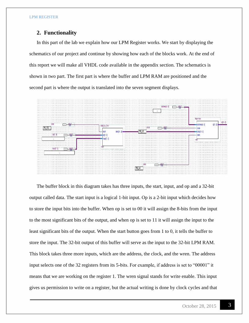
In this part of the lab we explain how our LPM Register works. We start by displaying the
schematics of our project and continue by showing how each of the blocks work. At the end of
this report we will make all VHDL code available in the appendix section. The schematics is
shown in two part. The first part is where the buffer and LPM RAM are positioned and the
second part is where the output is translated into the seven segment displays.
The buffer block in this diagram takes has three inputs, the start, input, and op and a 32-bit
output called data. The start input is a logical 1-bit input. Op is a 2-bit input which decides how
to store the input bits into the buffer. When op is set to 00 it will assign the 8-bits from the input
to the most significant bits of the output, and when op is set to 11 it will assign the input to the
least significant bits of the output. When the start button goes from 1 to 0, it tells the buffer to
store the input. The 32-bit output of this buffer will serve as the input to the 32-bit LPM RAM.
This block takes three more inputs, which are the address, the clock, and the wren. The address
input selects one of the 32 registers from its 5-bits. For example, if address is set to “00001” it
means that we are working on the register 1. The wren signal stands for write enable. This input
gives us permission to write on a register, but the actual writing is done by clock cycles and that
LPM REGISTER
4 October 28, 2015
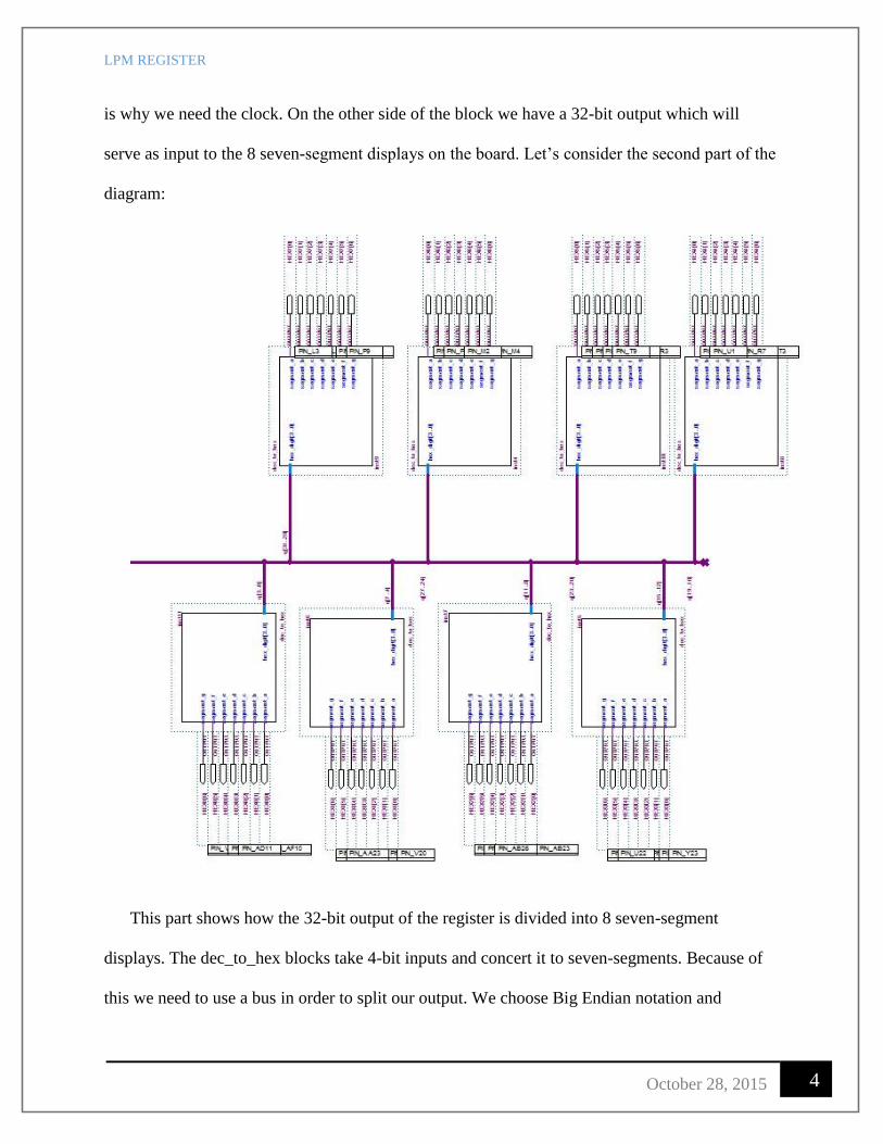
is why we need the clock. On the other side of the block we have a 32-bit output which will
serve as input to the 8 seven-segment displays on the board. Let’s consider the second part of the
diagram:
This part shows how the 32-bit output of the register is divided into 8 seven-segment
displays. The dec_to_hex blocks take 4-bit inputs and concert it to seven-segments. Because of
this we need to use a bus in order to split our output. We choose Big Endian notation and

LPM REGISTER
5 October 28, 2015
therefore the leftmost display will contain the most significant bits and the least significant bits
will be stored in the rightmost display. We tell the bus nodes which part of the output they are
going to take and in this way we assign correct display. For example, the four bits from 31 to 28,
which are the most significant bits of the output will be fed into the HEX7 display and the 3 to 0
bits will be fed into the HEX0 display. In this way we have our 32-bit output displayed in
hexadecimal notation on eight seven-segment displays.
LPM REGISTER
6 October 28, 2015
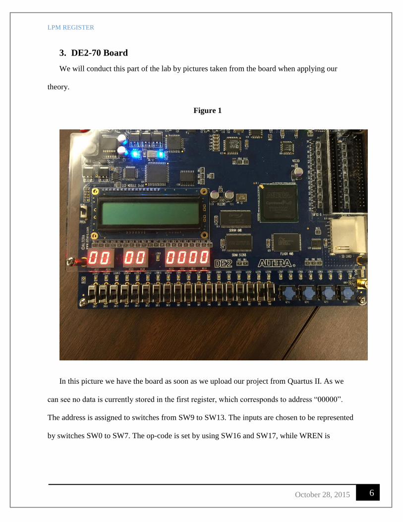
3. DE2-70 Board
We will conduct this part of the lab by pictures taken from the board when applying our
theory.
Figure 1
In this picture we have the board as soon as we upload our project from Quartus II. As we
can see no data is currently stored in the first register, which corresponds to address “00000”.
The address is assigned to switches from SW9 to SW13. The inputs are chosen to be represented
by switches SW0 to SW7. The op-code is set by using SW16 and SW17, while WREN is
LPM REGISTER
7 October 28, 2015
controlled by SW15 and the clock is on SW14. Switch number 8 does not have any effect on our
circuit.
Another thing to notice is that the “start” input of the buffer is assigned to KEY2 on the right
hand side of the board and we cannot show its position because that is a button and is pressed
and released.
The seven-segment displays show the number “00000000” which is what we expected. To
keep this lab simple we will try to display the number 1 in hexadecimal on each of the displays.
This number will be stored in the register at address “00000” which is register 1. The inputs need
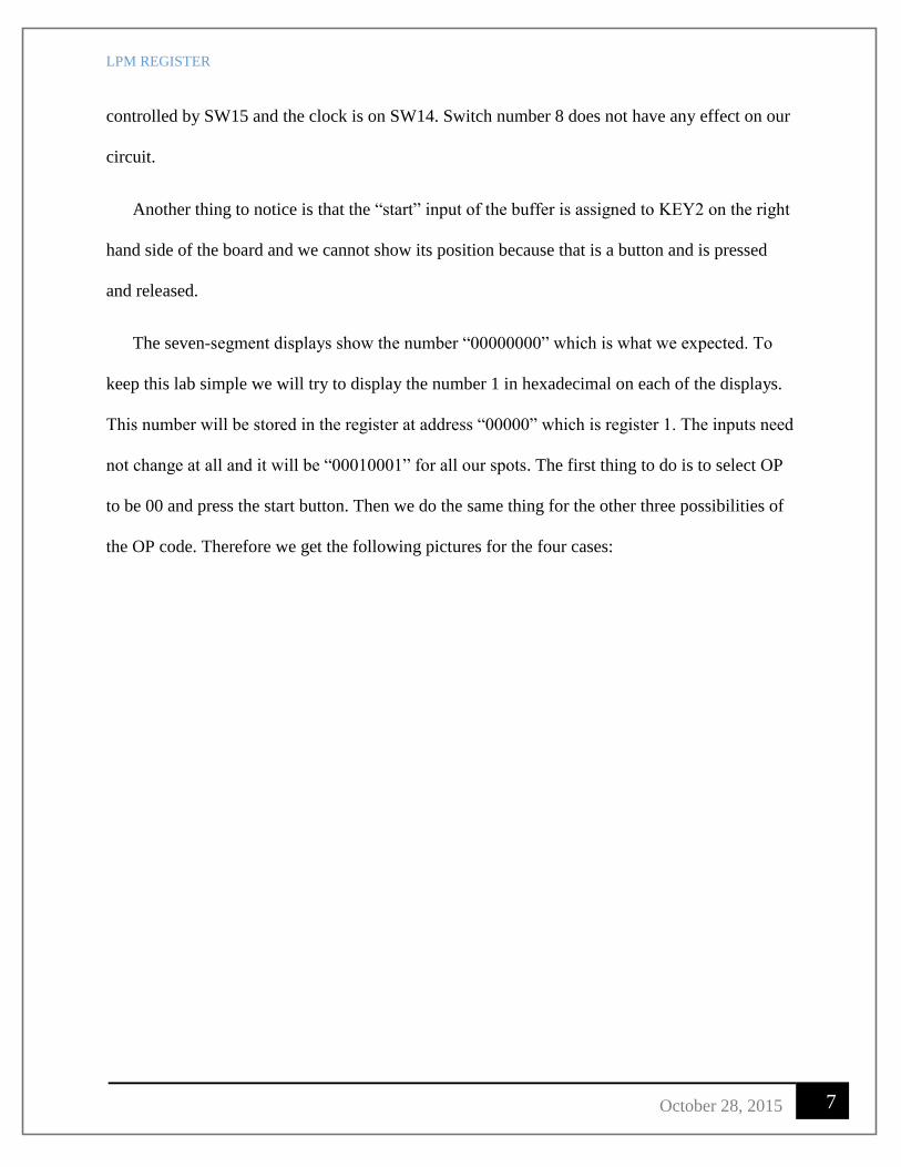
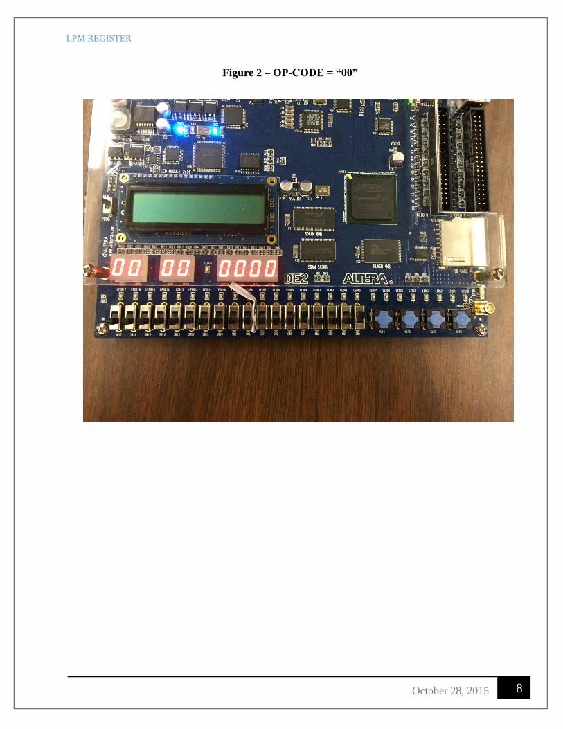
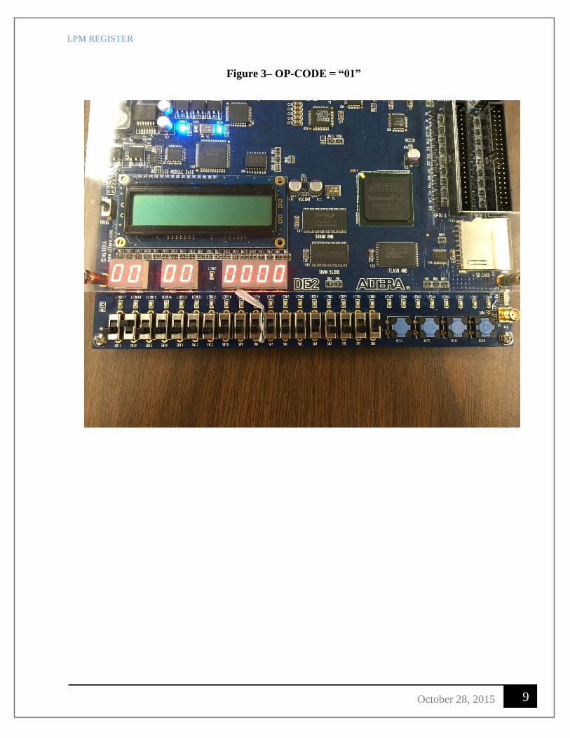
not change at all and it will be “00010001” for all our spots. The first thing to do is to select OP
to be 00 and press the start button. Then we do the same thing for the other three possibilities of
the OP code. Therefore we get the following pictures for the four cases:
LPM REGISTER
8 October 28, 2015
Figure 2 – OP-CODE = “00”
LPM REGISTER
9 October 28, 2015
Figure 3– OP-CODE = “01”
LPM REGISTER
10 October 28, 2015
Figure 4– OP-CODE = “10”
LPM REGISTER
11 October 28, 2015
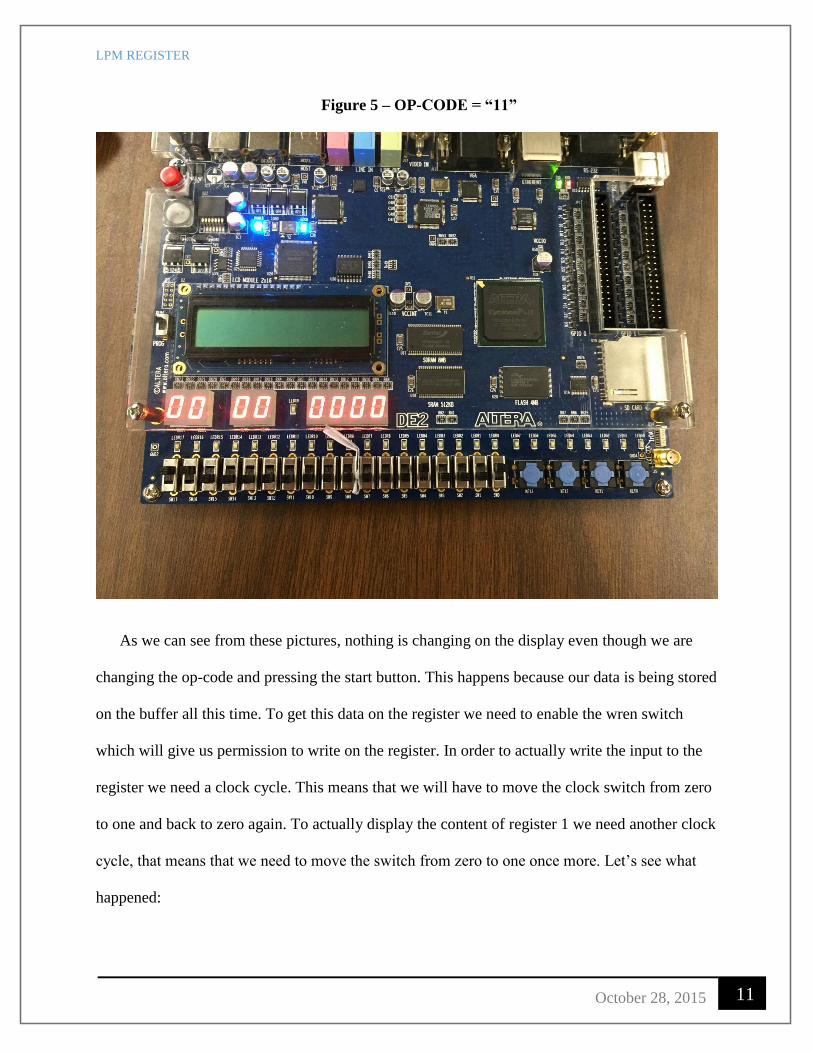
Figure 5 – OP-CODE = “11”
As we can see from these pictures, nothing is changing on the display even though we are
changing the op-code and pressing the start button. This happens because our data is being stored
on the buffer all this time. To get this data on the register we need to enable the wren switch
which will give us permission to write on the register. In order to actually write the input to the
register we need a clock cycle. This means that we will have to move the clock switch from zero
to one and back to zero again. To actually display the content of register 1 we need another clock
cycle, that means that we need to move the switch from zero to one once more. Let’s see what
happened:
LPM REGISTER
12 October 28, 2015
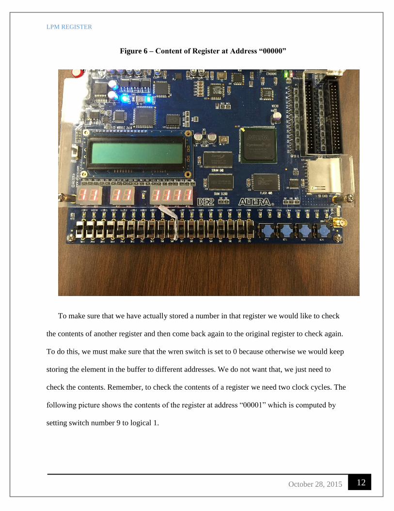
Figure 6 – Content of Register at Address “00000”
To make sure that we have actually stored a number in that register we would like to check
the contents of another register and then come back again to the original register to check again.
To do this, we must make sure that the wren switch is set to 0 because otherwise we would keep
storing the element in the buffer to different addresses. We do not want that, we just need to
check the contents. Remember, to check the contents of a register we need two clock cycles. The
following picture shows the contents of the register at address “00001” which is computed by
setting switch number 9 to logical 1.
LPM REGISTER
13 October 28, 2015
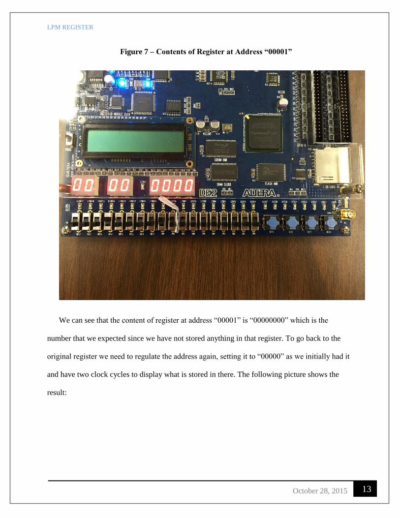
Figure 7 – Contents of Register at Address “00001”
We can see that the content of register at address “00001” is “00000000” which is the
number that we expected since we have not stored anything in that register. To go back to the
original register we need to regulate the address again, setting it to “00000” as we initially had it
and have two clock cycles to display what is stored in there. The following picture shows the
result:
LPM REGISTER
14 October 28, 2015
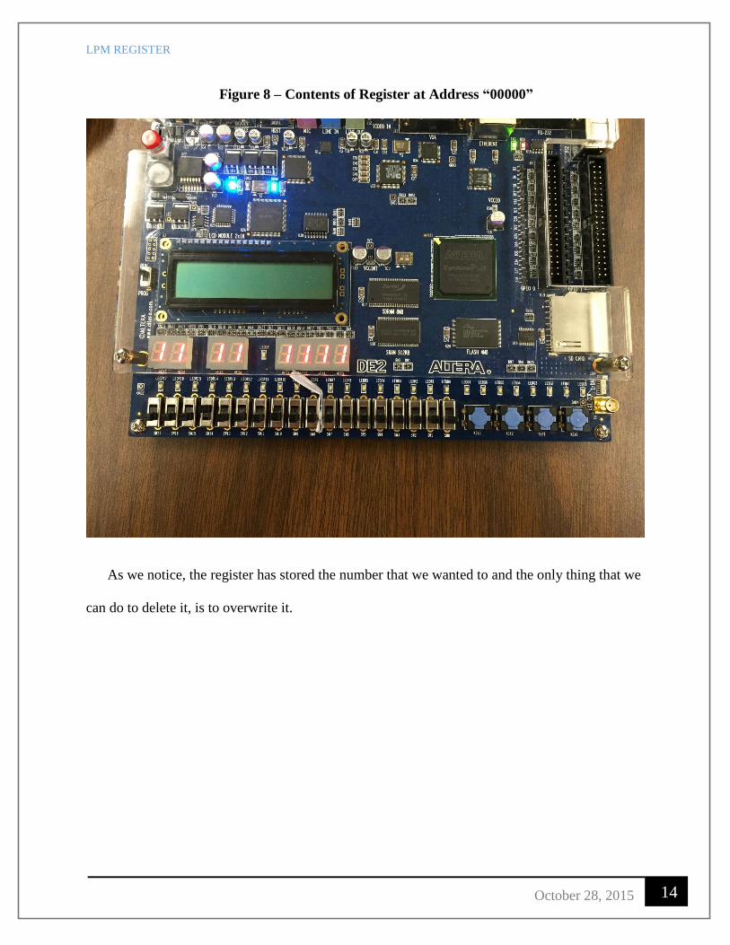
Figure 8 – Contents of Register at Address “00000”
As we notice, the register has stored the number that we wanted to and the only thing that we
can do to delete it, is to overwrite it.
LPM REGISTER
15 October 28, 2015
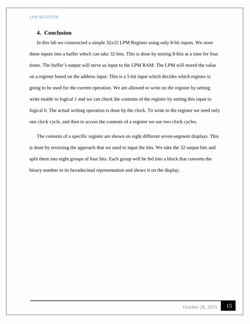
4. Conclusion
In this lab we constructed a simple 32x32 LPM Register using only 8-bit inputs. We store
these inputs into a buffer which can take 32-bits. This is done by storing 8-bits at a time for four
times. The buffer’s output will serve as input to the LPM RAM. The LPM will stored the value
on a register based on the address input. This is a 5-bit input which decides which register is
going to be used for the current operation. We are allowed to write on the register by setting
write enable to logical 1 and we can check the contents of the register by setting this input to
logical 0. The actual writing operation is done by the clock. To write to the register we need only
one clock cycle, and then to access the contents of a register we use two clock cycles.
The contents of a specific register are shown on eight different seven-segment displays. This
is done by reversing the approach that we used to input the bits. We take the 32 output bits and
split them into eight groups of four bits. Each group will be fed into a block that converts the
binary number to its hexadecimal representation and shows it on the display.
LPM REGISTER
16 October 28, 2015
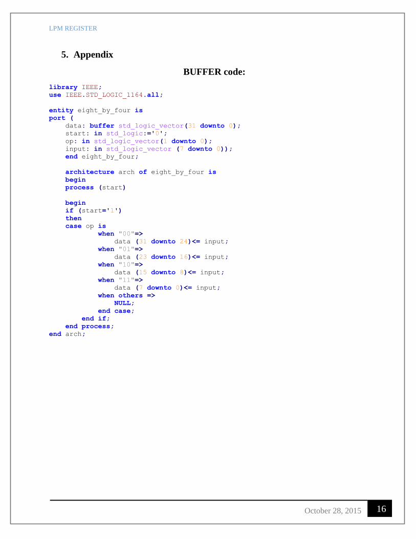
5. Appendix
BUFFER code:
library IEEE;
use IEEE.STD_LOGIC_1164.all;
entity eight_by_four is
port (
data: buffer std_logic_vector(31 downto 0);
start: in std_logic:='0';
op: in std_logic_vector(1 downto 0);
input: in std_logic_vector (7 downto 0));
end eight_by_four;
architecture arch of eight_by_four is
begin
process (start)
begin
if (start='1')
then
case op is
when "00"=>
data (31 downto 24)<= input;
when "01"=>
data (23 downto 16)<= input;
when "10"=>
data (15 downto 8)<= input;
when "11"=>
data (7 downto 0)<= input;
when others =>
NULL;
end case;
end if;
end process;
end arch;
LPM REGISTER
17 October 28, 2015
DEC_to_HEX code:
LIBRARY IEEE;
USE IEEE.STD_LOGIC_1164.ALL;
USE IEEE.STD_LOGIC_ARITH.ALL;
USE IEEE.STD_LOGIC_UNSIGNED.ALL;
-- Hexadecimal to 7 Segment Decoder for LED Display
ENTITY dec_to_hex IS
PORT( hex_digit : IN STD_LOGIC_VECTOR(3 DOWNTO 0);
segment_a, segment_b, segment_c, segment_d, segment_e, segment_f,
segment_g: OUT std_logic);
END dec_to_hex;
ARCHITECTURE a OF dec_to_hex IS
SIGNAL segment_data : STD_LOGIC_VECTOR(6 DOWNTO 0);
BEGIN
PROCESS (Hex_digit)
-- HEX to 7 segment Decoder for LED Display
BEGIN -- Hex-digit is the four bit binary value to display
CASE Hex_digit IS
WHEN "0000" =>
segment_data <= "1111110";
WHEN "0001" =>
segment_data <= "0110000";
WHEN "0010" =>
segment_data <= "1101101";
WHEN "0011" =>
segment_data <= "1111001";
WHEN "0100" =>
segment_data <= "0110011";
WHEN "0101" =>
segment_data <= "1011011";
WHEN "0110" =>
segment_data <= "1011111";
WHEN "0111" =>
segment_data <= "1110000";
WHEN "1000" =>
segment_data <= "1111111";
WHEN "1001" =>
segment_data <= "1110011";
WHEN "1010" =>
segment_data <= "1110111";
WHEN "1011" =>
segment_data <= "0011111";
WHEN "1100" =>
segment_data <= "1001110";
WHEN "1101" =>
segment_data <= "0111101";
WHEN "1110" =>
segment_data <= "1001111";
WHEN "1111" =>
segment_data <= "1000111";
END CASE;
END PROCESS;
-- extract segment data bits and invert
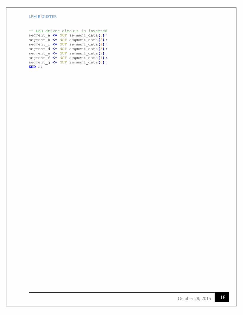
LPM REGISTER
18 October 28, 2015
-- LED driver circuit is inverted
segment_a <= NOT segment_data(6);
segment_b <= NOT segment_data(5);
segment_c <= NOT segment_data(4);
segment_d <= NOT segment_data(3);
segment_e <= NOT segment_data(2);
segment_f <= NOT segment_data(1);
segment_g <= NOT segment_data(0);
END a;