Embed Size (px)
Citation preview

LP3962, LP3965
www.ti.com SNVS066H –MAY 2000–REVISED APRIL 2013
LP3962/LP3965 1.5A Fast Ultra Low Dropout Linear RegulatorsCheck for Samples: LP3962, LP3965
1FEATURES DESCRIPTIONThe LP3962/LP3965 series of fast ultra low-dropout
2• Ultra Low Dropout Voltagelinear regulators operate from a +2.5V to +7.0V input
• Low Ground Pin Current supply. Wide range of preset output voltage options• Load Regulation of 0.04% are available. These ultra low dropout linear
regulators respond very fast to step changes in load• 15µA Quiescent Current in Shutdown Modewhich makes them suitable for low voltage• Specified Output Current of 1.5A DC microprocessor applications. The LP3962/LP3965 are
• Available in SOT-223,SFM/TO-263 and TO-220 developed on a CMOS process which allows lowPackages quiescent current operation independent of output
load current. This CMOS process also allows the• Output Voltage Accuracy ± 1.5%LP3962/LP3965 to operate under extremely low• Error Flag Indicates Output Status (LP3962) dropout conditions.
• Sense Option Improves Better LoadDropout Voltage: Ultra low dropout voltage; typicallyRegulation (LP3965)38mV at 150mA load current and 380mV at 1.5A load
• Extremely Low Output Capacitor current.Requirements
Ground Pin Current: Typically 5mA at 1.5A load• Overtemperature/Overcurrent Protection current.• −40°C to +125°C Junction Temperature Range
Shutdown Mode: Typically 15µA quiescent currentwhen the shutdown pin is pulled low.APPLICATIONSError Flag: Error flag goes low when the output• Microprocessor Power Suppliesvoltage drops 10% below nominal value (for LP3962).
• GTL, GTL+, BTL, and SSTL Bus TerminatorsSENSE: Sense pin improves regulation at remote• Power Supplies for DSPsloads. (For LP3965)
• SCSI TerminatorPrecision Output Voltage: Multiple output voltage
• Post Regulators options are available ranging from 1.2V to 5.0V and• High Efficiency Linear Regulators adjustable (LP3965), with a specified accuracy of
±1.5% at room temperature, and ±3.0% over all• Battery Chargersconditions (varying line, load, and temperature).• Other Battery Powered Applications
Typical Application Circuits
*SD and ERROR pins must be pulled high through a 10kΩ pull-up resistor. Connect the ERROR pin to ground if thisfunction is not used. See Application Hints section for more information.
1
Please be aware that an important notice concerning availability, standard warranty, and use in critical applications ofTexas Instruments semiconductor products and disclaimers thereto appears at the end of this data sheet.
2All trademarks are the property of their respective owners.
PRODUCTION DATA information is current as of publication date. Copyright © 2000–2013, Texas Instruments IncorporatedProducts conform to specifications per the terms of the TexasInstruments standard warranty. Production processing does notnecessarily include testing of all parameters.

LP3962, LP3965
SNVS066H –MAY 2000–REVISED APRIL 2013 www.ti.com
*SD and ERROR pins must be pulled high through a 10kΩ pull-up resistor. Connect the ERROR pin to ground if thisfunction is not used. See Application Hints section for more information.
Block Diagram LP3962
2 Submit Documentation Feedback Copyright © 2000–2013, Texas Instruments Incorporated
Product Folder Links: LP3962 LP3965
LP3962, LP3965
www.ti.com SNVS066H –MAY 2000–REVISED APRIL 2013
Block Diagram LP3965
Block Diagram LP3965-ADJ
Connection Diagram
Figure 1. Top View Figure 2. Top View Figure 3. Top ViewSOT-223-5 Package TO-220-5 Package SFM/TO-263-5 Package
Bent, Staggered Leads
Copyright © 2000–2013, Texas Instruments Incorporated Submit Documentation Feedback 3
Product Folder Links: LP3962 LP3965

LP3962, LP3965
SNVS066H –MAY 2000–REVISED APRIL 2013 www.ti.com
Pin Descriptions for SOT-223-5 PackageLP3962 LP3965
Pin #Name Function Name Function
1 SD Shutdown SD Shutdown
2 VIN Input Supply VIN Input Supply
3 VOUT Output Voltage VOUT Output Voltage
4 ERROR ERROR Flag SENSE/ADJ Remote Sense Pin or OutputAdjust Pin
5 GND Ground GND Ground
Pin Descriptions for TO-220-5 and SFM/TO-263-5 PackagesLP3962 LP3965
Pin #Name Function Name Function
1 SD Shutdown SD Shutdown
2 VIN Input Supply VIN Input Supply
3 GND Ground GND Ground
4 VOUT Output Voltage VOUT Output Voltage
5 ERROR ERROR Flag SENSE/ADJ Remote Sense Pin or OutputAdjust Pin
These devices have limited built-in ESD protection. The leads should be shorted together or the device placed in conductive foamduring storage or handling to prevent electrostatic damage to the MOS gates.
Absolute Maximum Ratings (1) (2)
Storage Temperature Range −65°C to +150°C
Lead Temperature (Soldering, 5 sec.) 260°C
ESD Rating (3) 2 kV
Power Dissipation (4) Internally Limited
Input Supply Voltage (Survival) −0.3V to +7.5V
Shutdown Input Voltage (Survival) −0.3V to VIN+0.3V
Output Voltage (Survival), (5), (6) −0.3V to +7.5V
IOUT (Survival) Short Circuit Protected
Maximum Voltage for ERROR Pin VIN+0.3V
Maximum Voltage for SENSE Pin VOUT+0.3V
(1) Absolute maximum ratings indicate limits beyond which damage to the device may occur. Operating ratings indicate conditions for whichthe device is intended to be functional, but does not ensure specific performance limits. For ensured specifications and test conditions,see Electrical Characteristics. The ensured specifications apply only for the test conditions listed. Some performance characteristics maydegrade when the device is not operated under the listed test conditions.
(2) If Military/Aerospace specified devices are required, please contact the TI Sales Office/ Distributors for availability and specifications.(3) The human body model is a 100pF capacitor discharged through a 1.5kΩ resistor into each pin.(4) At elevated temperatures, devices must be derated based on package thermal resistance. The devices in TO-220 package must be
derated at θjA = 50°C/W (with 0.5in2, 1oz. copper area), junction-to-ambient (with no heat sink). The devices in the SFM/TO-263surface-mount package must be derated at θjA = 60°C/W (with 0.5in2, 1oz. copper area), junction-to-ambient. The devices in SOT-223package must be derated at θjA = 90°C/W (with 0.5in2, 1oz. copper area), junction-to-ambient.
(5) If used in a dual-supply system where the regulator load is returned to a negative supply, the LP396X output must be diode-clamped toground.
(6) The output PMOS structure contains a diode between the VIN and VOUT terminals. This diode is normally reverse biased. This diode willget forward biased if the voltage at the output terminal is forced to be higher than the voltage at the input terminal. This diode cantypically withstand 200mA of DC current and 1Amp of peak current.
4 Submit Documentation Feedback Copyright © 2000–2013, Texas Instruments Incorporated
Product Folder Links: LP3962 LP3965
LP3962, LP3965
www.ti.com SNVS066H –MAY 2000–REVISED APRIL 2013
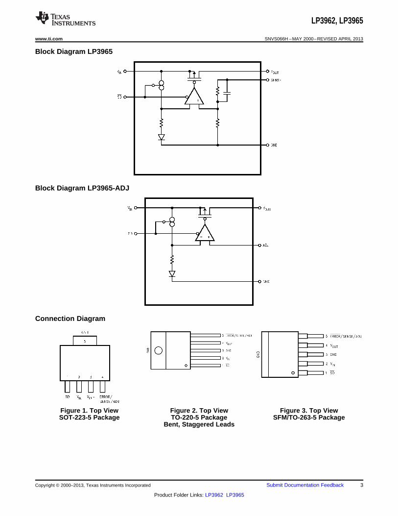
Operating RatingsInput Supply Voltage (Operating), (1) 2.5V to 7.0V
Shutdown Input Voltage (Operating) −0.3V to VIN+0.3V
Maximum Operating Current (DC) 1.5A
Operating Junction Temp. Range −40°C to +125°C
(1) The minimum operating value for VIN is equal to either [VOUT(NOM) + VDROPOUT] or 2.5V, whichever is greater.
Electrical CharacteristicsLP3962/LP3965Limits in standard typeface are for TJ = 25°C, and limits in boldface type apply over the full operating temperature range.Unless otherwise specified: VIN = VO(NOM) + 1V, IL = 10 mA, COUT = 33µF, VSD = VIN-0.3V.
Symbol Parameter Conditions Typ (1) LP3962/5 (2) Units
Min Max
VO Output Voltage Tolerance (3) 10 mA ≤ IL ≤ 1.5A -1.5 +1.50 %VOUT +1 ≤ VIN≤ 7.0V -3.0 +3.0
VADJ Adjust Pin Voltage (ADJ version) 10 mA ≤ IL ≤ 1.5A 1.198 1.2341.216 VVOUT +1.5V ≤ VIN≤ 7.0V 1.180 1.253
ΔV OL Output Voltage Line Regulation VOUT+1V<VIN<7.0V, 0.02 %(3) 0.06
ΔVO/ ΔIOUT Output Voltage Load 10 mA < IL < 1.5 A 0.04 %Regulation (3) 0.09
VIN - VOUT IL = 150 mA 38 4555
Dropout Voltage (4) mVIL = 1.5 A 380 450
550
IL = 150 mA 4 910Ground Pin Current In NormalIGND mAOperation Mode IL = 1.5 A 5 1415
IGND Ground Pin Current In Shutdown VSD ≤ 0.2V 15 25 µAMode (5) 75
IO(PK) Peak Output Current See (6) 2.5 2.0 A1.7
SHORT CIRCUIT PROTECTION
ISC Short Circuit Current 4.5 A
OVER TEMPERATURE PROTECTION
Tsh(t) Shutdown Threshold 165 °C
Tsh(h) Thermal Shutdown Hysteresis 10 °C
SHUTDOWN INPUT
Output = High VIN VIN–0.3VSDT Shutdown Threshold V
Output = Low 0 0.2
TdOFF Turn-off delay IL = 1.5 A 20 µs
(1) Typical numbers are at 25°C and represent the most likely parametric norm.(2) Limits are 100% production tested at 25°C. Limits over the operating temperature range are specified through correlation using
Statistical Quality Control (SQC) methods. The limits are used to calculate TI's Average Outgoing Quality Level (AOQL).(3) Output voltage line regulation is defined as the change in output voltage from the nominal value due to change in the input line voltage.
Output voltage load regulation is defined as the change in output voltage from the nominal value due to change in load current. The lineand load regulation specification contains only the typical number. However, the limits for line and load regulation are included in theoutput voltage tolerance specification.
(4) Dropout voltage is defined as the minimum input to output differential voltage at which the output drops 2% below the nominal value.Dropout voltage specification applies only to output voltages of 2.5V and above. For output voltages below 2.5V, the drop-out voltage isnothing but the input to output differential, since the minimum input voltage is 2.5V.
(5) This specification has been tested for −40°C ≤ TJ ≤ 85°C since the temperature rise of the device is negligible under shutdownconditions.
(6) At elevated temperatures, devices must be derated based on package thermal resistance. The devices in TO-220 package must bederated at θjA = 50°C/W (with 0.5in2, 1oz. copper area), junction-to-ambient (with no heat sink). The devices in the SFM/TO-263surface-mount package must be derated at θjA = 60°C/W (with 0.5in2, 1oz. copper area), junction-to-ambient. The devices in SOT-223package must be derated at θjA = 90°C/W (with 0.5in2, 1oz. copper area), junction-to-ambient.
Copyright © 2000–2013, Texas Instruments Incorporated Submit Documentation Feedback 5
Product Folder Links: LP3962 LP3965

LP3962, LP3965
SNVS066H –MAY 2000–REVISED APRIL 2013 www.ti.com
Electrical CharacteristicsLP3962/LP3965 (continued)Limits in standard typeface are for TJ = 25°C, and limits in boldface type apply over the full operating temperature range.Unless otherwise specified: VIN = VO(NOM) + 1V, IL = 10 mA, COUT = 33µF, VSD = VIN-0.3V.
Symbol Parameter Conditions Typ (1) LP3962/5 (2) Units
Min Max
TdON Turn-on delay IL = 1.5 A 25 µs
ISD SD Input Current VSD = VIN 1 nA
ERROR FLAG COMPARATOR
VT Threshold See (7) 10 5 16 %
VTH Threshold Hysteresis See (7) 5 2 8 %
VEF(Sat) Error Flag Saturation Isink = 100µA 0.02 0.1 V
Td Flag Reset Delay 1 µs
Ilk Error Flag Pin Leakage Current 1 nA
Imax Error Flag Pin Sink Current VError = 0.5V (over temp.) 1 mA
AC PARAMETERS
VIN = VOUT + 1.5V 60COUT = 100uFVOUT = 3.3V
PSRR Ripple Rejection dBVIN = VOUT + 0.3V 40COUT = 100uFVOUT = 3.3V
ρn(l/f Output Noise Density f = 120Hz 0.8 µV
BW = 10Hz – 100kHz 150en Output Noise Voltage (rms) µV (rms)
BW = 300Hz – 300kHz 100
(7) Error Flag threshold and hysteresis are specified as percentage of regulated output voltage.
6 Submit Documentation Feedback Copyright © 2000–2013, Texas Instruments Incorporated
Product Folder Links: LP3962 LP3965

LP3962, LP3965
www.ti.com SNVS066H –MAY 2000–REVISED APRIL 2013
Typical Performance CharacteristicsUnless otherwise specified, VIN =VO(NOM) + 1V, VOUT= 2.5V, COUT = 33µF, IOUT = 10mA, CIN = 68µF, VSD = VIN, and TA = 25°C.
Drop-Out Voltage Drop-Out Voltagevs vs
Temperature for Different Load Currents Temperature for Different Output Voltages (IOUT = 800mA
Figure 4. Figure 5.
Ground Pin Current Ground Pin Currentvs vs
Input Voltage (VSD=VIN) Input Voltage (VSD=100mV)
Figure 6. Figure 7.
Ground Current Ground Currentvs vs
Temperature (VSD=VIN) Temperature (VSD=0V
Figure 8. Figure 9.
Copyright © 2000–2013, Texas Instruments Incorporated Submit Documentation Feedback 7
Product Folder Links: LP3962 LP3965

LP3962, LP3965
SNVS066H –MAY 2000–REVISED APRIL 2013 www.ti.com
Typical Performance Characteristics (continued)Unless otherwise specified, VIN =VO(NOM) + 1V, VOUT= 2.5V, COUT = 33µF, IOUT = 10mA, CIN = 68µF, VSD = VIN, and TA = 25°C.
Ground Pin Current Input Voltagevs vs
Shutdown Pin Voltage Output Voltage
Figure 10. Figure 11.
Output Noise Density, VOUT= 2.5V Output Noise Density, VOUT= 5V
Figure 12. Figure 13.
Ripple Rejectionvs
Load Transient Response Frequency
Figure 14. Figure 15.
8 Submit Documentation Feedback Copyright © 2000–2013, Texas Instruments Incorporated
Product Folder Links: LP3962 LP3965

LP3962, LP3965
www.ti.com SNVS066H –MAY 2000–REVISED APRIL 2013
Typical Performance Characteristics (continued)Unless otherwise specified, VIN =VO(NOM) + 1V, VOUT= 2.5V, COUT = 33µF, IOUT = 10mA, CIN = 68µF, VSD = VIN, and TA = 25°C.
δVOUTvs
Temperature Noise Density VIN = 3.5V, VOUT = 2.5V, IL = 10 mA
Figure 16. Figure 17.
Line Transient Response Line Transient Response
Figure 18. Figure 19.
Line Transient Response (IOUT = 1.5A) Line Transient Response (IOUT = 1.5A)
Figure 20. Figure 21.
Copyright © 2000–2013, Texas Instruments Incorporated Submit Documentation Feedback 9
Product Folder Links: LP3962 LP3965

LP3962, LP3965
SNVS066H –MAY 2000–REVISED APRIL 2013 www.ti.com
APPLICATIONS INFORMATION
EXTERNAL CAPACITORS
Like any low-dropout regulator, external capacitors are required to assure stability. these capacitors must becorrectly selected for proper performance.
INPUT CAPACITOR: The LP3962/5 requires a low source impedance to maintain regulator stability because theinternal bias circuitry is connected directly to VIN. The input capacitor must be located less than 1 cm from theLP3962/5 device and connected directly to the input and ground pins using traces which have no other currentsflowing through them (see PCB LAYOUT).
The minimum allowable input capacitance for a given application depends on the type of the capacitor and ESR(equivalent series resistance). A lower ESR capacitor allows the use of less capacitance, while higher ESR types(like aluminum electrolytics) require more capacitance.
The lowest value of input capacitance that can be used for stable full-load operation is 68 µF (assuming it is aceramic or low-ESR Tantalum with ESR less than 100 mΩ).
To determine the minimum input capacitance amount and ESR value, an approximation which should be used is:CIN ESR (mΩ) / CIN (µF) ≤ 1.5
This shows that input capacitors with higher ESR values can be used if sufficient total capacitance is provided.Capacitor types (aluminum, ceramic, and tantalum) can be mixed in parallel, but the total equivalent inputcapacitance/ESR must be defined as above to assure stable operation.
IMPORTANT: The input capacitor must maintain its ESR and capacitance in the "stable range" over the entiretemperature range of the application to assure stability (see CAPACITOR CHARACTERISTICS).
OUTPUT CAPACITOR: An output capacitor is also required for loop stability. It must be located less than 1 cmfrom the LP3962/5 device and connected directly to the output and ground pins using traces which have no othercurrents flowing through them (see PCB LAYOUT).
The minimum value of the output capacitance that can be used for stable full-load operation is 33 µF, but it maybe increased without limit. The output capacitor's ESR is critical because it forms a zero to provide phase leadwhich is required for loop stability. The ESR must fall within the specified range:
0.2Ω ≤ COUT ESR ≤ 5Ω
The lower limit of 200 mΩ means that ceramic capacitors are not suitable for use as LP3962/5 output capacitors(but can be used on the input). Some ceramic capacitance can be used on the output if the total equivalent ESRis in the stable range: when using a 100 µF Tantalum as the output capacitor, approximately 3 µF of ceramiccapacitance can be applied before stability becomes marginal.
IMPORTANT: The output capacitor must meet the requirements for minimum amount of capacitance and alsohave an appropriate ESR value over the full temperature range of the application to assure stability (seeCAPACITOR CHARACTERISTICS).
SELECTING A CAPACITOR
It is important to note that capacitance tolerance and variation with temperature must be taken into considerationwhen selecting a capacitor so that the minimum required amount of capacitance is provided over the fulloperating temperature range. In general, a good Tantalum capacitor will show very little capacitance variationwith temperature, but a ceramic may not be as good (depending on dielectric type). Aluminum electrolytics alsotypically have large temperature variation of capacitance value.
Equally important to consider is a capacitor's ESR change with temperature: this is not an issue with ceramics,as their ESR is extremely low. However, it is very important in Tantalum and aluminum electrolytic capacitors.Both show increasing ESR at colder temperatures, but the increase in aluminum electrolytic capacitors is sosevere they may not be feasible for some applications (see CAPACITOR CHARACTERISTICS).
10 Submit Documentation Feedback Copyright © 2000–2013, Texas Instruments Incorporated
Product Folder Links: LP3962 LP3965
LP3962, LP3965
www.ti.com SNVS066H –MAY 2000–REVISED APRIL 2013
CAPACITOR CHARACTERISTICS
CERAMIC: For values of capacitance in the 10 to 100 µF range, ceramics are usually larger and more costlythan tantalums but give superior AC performance for bypassing high frequency noise because of very low ESR(typically less than 10 mΩ). However, some dielectric types do not have good capacitance characteristics as afunction of voltage and temperature.
Z5U and Y5V dielectric ceramics have capacitance that drops severely with applied voltage. A typical Z5U orY5V capacitor can lose 60% of its rated capacitance with half of the rated voltage applied to it. The Z5U and Y5Valso exhibit a severe temperature effect, losing more than 50% of nominal capacitance at high and low limits ofthe temperature range.
X7R and X5R dielectric ceramic capacitors are strongly recommended if ceramics are used, as they typicallymaintain a capacitance range within ±20% of nominal over full operating ratings of temperature and voltage. Ofcourse, they are typically larger and more costly than Z5U/Y5U types for a given voltage and capacitance.
TANTALUM: Solid Tantalum capacitors are recommended for use on the output because their typical ESR isvery close to the ideal value required for loop compensation. They also work well as input capacitors if selectedto meet the ESR requirements previously listed.
Tantalums also have good temperature stability: a good quality Tantalum will typically show a capacitance valuethat varies less than 10-15% across the full temperature range of 125°C to −40°C. ESR will vary only about 2Xgoing from the high to low temperature limits.
The increasing ESR at lower temperatures can cause oscillations when marginal quality capacitors are used (ifthe ESR of the capacitor is near the upper limit of the stability range at room temperature).
ALUMINUM: This capacitor type offers the most capacitance for the money. The disadvantages are that they arelarger in physical size, not widely available in surface mount, and have poor AC performance (especially athigher frequencies) due to higher ESR and ESL.
Compared by size, the ESR of an aluminum electrolytic is higher than either Tantalum or ceramic, and it alsovaries greatly with temperature. A typical aluminum electrolytic can exhibit an ESR increase of as much as 50Xwhen going from 25°C down to −40°C.
It should also be noted that many aluminum electrolytics only specify impedance at a frequency of 120 Hz, whichindicates they have poor high frequency performance. Only aluminum electrolytics that have an impedancespecified at a higher frequency (between 20 kHz and 100 kHz) should be used for the LP396X. Derating must beapplied to the manufacturer's ESR specification, since it is typically only valid at room temperature.
Any applications using aluminum electrolytics should be thoroughly tested at the lowest ambient operatingtemperature where ESR is maximum.
PCB LAYOUT
Good PC layout practices must be used or instability can be induced because of ground loops and voltage drops.The input and output capacitors must be directly connected to the input, output, and ground pins of the LP3962/5using traces which do not have other currents flowing in them Kelvin connect).
The best way to do this is to lay out CIN and COUT near the device with short traces to the VIN, VOUT, and groundpins. The regulator ground pin should be connected to the external circuit ground so that the regulator and itscapacitors have a "single point ground".
It should be noted that stability problems have been seen in applications where "vias" to an internal ground planewere used at the ground points of the LP3962/5 IC and the input and output capacitors. This was caused byvarying ground potentials at these nodes resulting from current flowing through the ground plane. Using a singlepoint ground technique for the regulator and it's capacitors fixed the problem.
Since high current flows through the traces going into VIN and coming from VOUT, Kelvin connect the capacitorleads to these pins so there is no voltage drop in series with the input and output capacitors.
Copyright © 2000–2013, Texas Instruments Incorporated Submit Documentation Feedback 11
Product Folder Links: LP3962 LP3965

LP3962, LP3965
SNVS066H –MAY 2000–REVISED APRIL 2013 www.ti.com
RFI/EMI SUSCEPTIBILITY
RFI (radio frequency interference) and EMI (electromagnetic interference) can degrade any integrated circuit'sperformance because of the small dimensions of the geometries inside the device. In applications where circuitsources are present which generate signals with significant high frequency energy content (> 1 MHz), care mustbe taken to ensure that this does not affect the IC regulator.
If RFI/EMI noise is present on the input side of the LP396X regulator (such as applications where the inputsource comes from the output of a switching regulator), good ceramic bypass capacitors must be used at theinput pin of the LP396X.
If a load is connected to the LP396X output which switches at high speed (such as a clock), the high-frequencycurrent pulses required by the load must be supplied by the capacitors on the LP396X output. Since thebandwidth of the regulator loop is less than 100 kHz, the control circuitry cannot respond to load changes abovethat frequency. The means the effective output impedance of the LP396X at frequencies above 100 kHz isdetermined only by the output capacitor(s).
In applications where the load is switching at high speed, the output of the LP396X may need RF isolation fromthe load. It is recommended that some inductance be placed between the LP396X output capacitor and the load,and good RF bypass capacitors be placed directly across the load.
PCB layout is also critical in high noise environments, since RFI/EMI is easily radiated directly into PC traces.Noisy circuitry should be isolated from "clean" circuits where possible, and grounded through a separate path. AtMHz frequencies, ground planes begin to look inductive and RFI/EMI can cause ground bounce across theground plane.
In multi-layer PCB applications, care should be taken in layout so that noisy power and ground planes do notradiate directly into adjacent layers which carry analog power and ground.
OUTPUT ADJUSTMENT
An adjustable output device has output voltage range of 1.216V to 5.1V. To obtain a desired output voltage, canbe used with R1 always a 10kΩ resistor.
For output stability, CF must be between 68pF and 100pF.
TURN-ON CHARACTERISTICS FOR OUTPUT VOLTAGES PROGRAMMED TO 2.0V OR BELOW
As Vin increases during start-up, the regulator output will track the input until Vin reaches the minimum operatingvoltage (typically about 2.2V). For output voltages programmed to 2.0V or below, the regulator output maymomentarily exceed its programmed output voltage during start up. Outputs programmed to voltages above 2.0Vare not affected by this behavior.
OUTPUT NOISE
Noise is specified in two ways-
Spot Noise or Output noise density is the RMS sum of all noise sources, measured at the regulator output, ata specific frequency (measured with a 1Hz bandwidth). This type of noise is usually plotted on a curve as afunction of frequency.
Total output Noise or Broad-band noise is the RMS sum of spot noise over a specified bandwidth, usuallyseveral decades of frequencies.
Attention should be paid to the units of measurement. Spot noise is measured in units µV/√Hz or nV/√Hz andtotal output noise is measured in µV(rms).
12 Submit Documentation Feedback Copyright © 2000–2013, Texas Instruments Incorporated
Product Folder Links: LP3962 LP3965

LP3962, LP3965
www.ti.com SNVS066H –MAY 2000–REVISED APRIL 2013
The primary source of noise in low-dropout regulators is the internal reference. In CMOS regulators, noise has alow frequency component and a high frequency component, which depend strongly on the silicon area andquiescent current. Noise can be reduced in two ways: by increasing the transistor area or by increasing thecurrent drawn by the internal reference. Increasing the area will decrease the chance of fitting the die into asmaller package. Increasing the current drawn by the internal reference increases the total supply current(ground pin current). Using an optimized trade-off of ground pin current and die size, LP3962/LP3965 achieveslow noise performance and low quiescent current operation.
The total output noise specification for LP3962/LP3965 is presented in the Electrical Characteristics table. TheOutput noise density at different frequencies is represented by a curve under typical performance characteristics.
SHORT-CIRCUIT PROTECTION
The LP3962and LP3965 is short circuit protected and in the event of a peak over-current condition, the short-circuit control loop will rapidly drive the output PMOS pass element off. Once the power pass element shutsdown, the control loop will rapidly cycle the output on and off until the average power dissipation causes thethermal shutdown circuit to respond to servo the on/off cycling to a lower frequency. Please refer to the sectionon thermal information for power dissipation calculations.
ERROR FLAG OPERATION
The LP3962/LP3965 produces a logic low signal at the Error Flag pin when the output drops out of regulationdue to low input voltage, current limiting, or thermal limiting. This flag has a built in hysteresis. The timingdiagram in Figure 22 shows the relationship between the ERROR and the output voltage. In this example, theinput voltage is changed to demonstrate the functionality of the Error Flag.
The internal Error flag comparator has an open drain output stage. Hence, the ERROR pin should be pulled highthrough a pull up resistor. Although the ERROR pin can sink current of 1mA, this current is energy drain from theinput supply. Hence, the value of the pull up resistor should be in the range of 10kΩ to 1MΩ. The ERROR pinmust be connected to ground if this function is not used. It should also be noted that when the shutdown pinis pulled low, the ERROR pin is forced to be invalid for reasons of saving power in shutdown mode.
Figure 22. Error Flag Operation
Copyright © 2000–2013, Texas Instruments Incorporated Submit Documentation Feedback 13
Product Folder Links: LP3962 LP3965

LP3962, LP3965
SNVS066H –MAY 2000–REVISED APRIL 2013 www.ti.com
SENSE PIN
In applications where the regulator output is not very close to the load, LP3965 can provide better remote loadregulation using the SENSE pin. Figure 23 depicts the advantage of the SENSE option. LP3962 regulates thevoltage at the output pin. Hence, the voltage at the remote load will be the regulator output voltage minus thedrop across the trace resistance. For example, in the case of a 3.3V output, if the trace resistance is 100mΩ, thevoltage at the remote load will be 3.15V with 1.5 A of load current, ILOAD. The LP3965 regulates the voltage at thesense pin. Connecting the sense pin to the remote load will provide regulation at the remote load, as shown inFigure 23. If the sense option pin is not required, the sense pin must be connected to the VOUT pin.
Figure 23. Improving remote load regulation using LP3965
SHUTDOWN OPERATION
A CMOS Logic level signal at the shutdown ( SD) pin will turn-off the regulator. Pin SD must be activelyterminated through a 10kΩ pull-up resistor for a proper operation. If this pin is driven from a source that activelypulls high and low (such as a CMOS rail to rail comparator), the pull-up resistor is not required. This pin must betied to Vin if not used.
DROPOUT VOLTAGE
The dropout voltage of a regulator is defined as the minimum input-to-output differential required to stay within2% of the output voltage. The LP3962/LP3965 use an internal MOSFET with an Rds(on) of 240mΩ (typically).For CMOS LDOs, the dropout voltage is the product of the load current and the Rds(on) of the internal MOSFET.
REVERSE CURRENT PATH
The internal MOSFET in LP3962and LP3965 has an inherent parasitic diode. During normal operation, the inputvoltage is higher than the output voltage and the parasitic diode is reverse biased. However, if the output ispulled above the input in an application, then current flows from the output to the input as the parasitic diode getsforward biased. The output can be pulled above the input as long as the current in the parasitic diode is limited to200mA continuous and 1A peak.
MAXIMUM OUTPUT CURRENT CAPABILITY
LP3962 and LP3965 can deliver a continuous current of 1.5 A over the full operating temperature range. Aheatsink may be required depending on the maximum power dissipation and maximum ambient temperature ofthe application. Under all possible conditions, the junction temperature must be within the range specified underoperating conditions. The total power dissipation of the device is given by:
PD = (VIN−VOUT)IOUT+ (VIN)IGND
14 Submit Documentation Feedback Copyright © 2000–2013, Texas Instruments Incorporated
Product Folder Links: LP3962 LP3965

LP3962, LP3965
www.ti.com SNVS066H –MAY 2000–REVISED APRIL 2013
where IGND is the operating ground current of the device (specified under Electrical Characteristics).
The maximum allowable temperature rise (TRmax) depends on the maximum ambient temperature (TAmax) of theapplication, and the maximum allowable junction temperature(TJmax):
TRmax = TJmax− TAmax
The maximum allowable value for junction to ambient Thermal Resistance, θJA, can be calculated using theformula:
θJA = TRmax / PD
LP3962 and LP3965 are available in TO-220, SFM/TO-263, and SOT-223 packages. The thermal resistancedepends on amount of copper area or heat sink, and on air flow. If the maximum allowable value of θJAcalculated above is ≥ 60 °C/W for TO-220 package, ≥60 °C/W for SFM/TO-263 package, and ≥ 140 °C/W forSOT-223 package, no heatsink is needed since the package can dissipate enough heat to satisfy theserequirements. If the value for allowable θJA falls below these limits, a heat sink is required.
HEATSINKING TO-220 PACKAGES
The thermal resistance of a TO-220 package can be reduced by attaching it to a heat sink or a copper plane ona PC board. If a copper plane is to be used, the values of θJA will be same as shown in next section for SFM/TO-263 package.
The heatsink to be used in the application should have a heatsink to ambient thermal resistance,
θHA≤ θJA − θCH − θJC.
In this equation, θCH is the thermal resistance from the junction to the surface of the heat sink and θJC is thethermal resistance from the junction to the surface of the case. θJC is about 3°C/W for a TO-220 package. Thevalue for θCH depends on method of attachment, insulator, etc. θCH varies between 1.5°C/W to 2.5°C/W. If theexact value is unknown, 2°C/W can be assumed.
HEATSINKING SFM/TO-263 AND SOT-223 PACKAGES
The SFM/TO-263 and SOT-223 packages use the copper plane on the PCB as a heatsink. The tab of thesepackages are soldered to the copper plane for heat sinking. Figure 24 shows a curve for the θJA of SFM/TO-263package for different copper area sizes, using a typical PCB with 1 ounce copper and no solder mask over thecopper area for heat sinking.
Figure 24. θJA vs Copper(1 Ounce) Area for SFM/TO-263 package
As shown in the figure, increasing the copper area beyond 1 square inch produces very little improvement. Theminimum value for θJA for the SFM/TO-263 packag mounted to a PCB is 32°C/W.
Figure 25 shows the maximum allowable power dissipation for SFM/TO-263 packages for different ambienttemperatures, assuming θJA is 35°C/W and the maximum junction temperature is 125°C.
Copyright © 2000–2013, Texas Instruments Incorporated Submit Documentation Feedback 15
Product Folder Links: LP3962 LP3965
LP3962, LP3965
SNVS066H –MAY 2000–REVISED APRIL 2013 www.ti.com
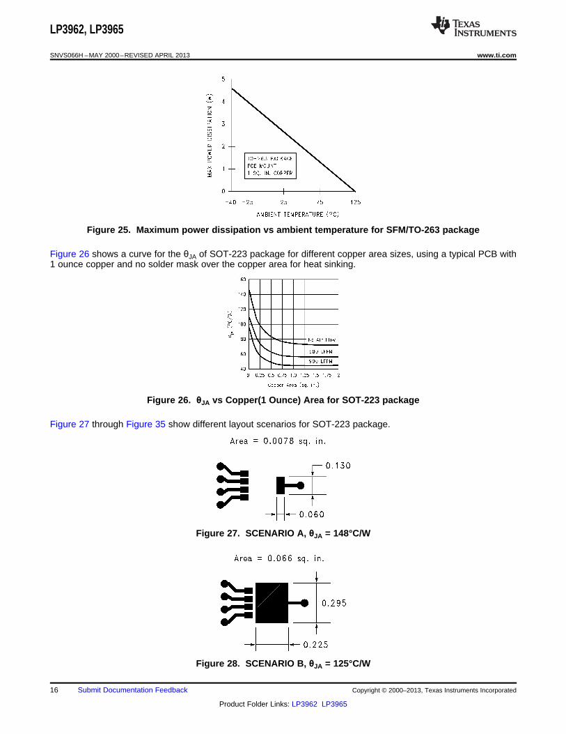
Figure 25. Maximum power dissipation vs ambient temperature for SFM/TO-263 package
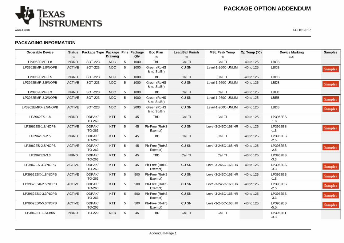
Figure 26 shows a curve for the θJA of SOT-223 package for different copper area sizes, using a typical PCB with1 ounce copper and no solder mask over the copper area for heat sinking.
Figure 26. θJA vs Copper(1 Ounce) Area for SOT-223 package
Figure 27 through Figure 35 show different layout scenarios for SOT-223 package.
Figure 27. SCENARIO A, θJA = 148°C/W
Figure 28. SCENARIO B, θJA = 125°C/W
16 Submit Documentation Feedback Copyright © 2000–2013, Texas Instruments Incorporated
Product Folder Links: LP3962 LP3965

LP3962, LP3965
www.ti.com SNVS066H –MAY 2000–REVISED APRIL 2013
Figure 29. SCENARIO C, θJA = 92°C/W
Figure 30. SCENARIO D, θJA = 83°C/W
Copyright © 2000–2013, Texas Instruments Incorporated Submit Documentation Feedback 17
Product Folder Links: LP3962 LP3965

LP3962, LP3965
SNVS066H –MAY 2000–REVISED APRIL 2013 www.ti.com
Figure 31. SCENARIO E, θJA = 77°C/W
Figure 32. SCENARIO F, θJA = 75°C/W
18 Submit Documentation Feedback Copyright © 2000–2013, Texas Instruments Incorporated
Product Folder Links: LP3962 LP3965

LP3962, LP3965
www.ti.com SNVS066H –MAY 2000–REVISED APRIL 2013
Figure 33. SCENARIO G, θJA = 113°C/W
Figure 34. SCENARIO H, θJA = 79°C/W
Copyright © 2000–2013, Texas Instruments Incorporated Submit Documentation Feedback 19
Product Folder Links: LP3962 LP3965

LP3962, LP3965
SNVS066H –MAY 2000–REVISED APRIL 2013 www.ti.com
Figure 35. SCENARIO I, θJA = 78.5°C/W
20 Submit Documentation Feedback Copyright © 2000–2013, Texas Instruments Incorporated
Product Folder Links: LP3962 LP3965

LP3962, LP3965
www.ti.com SNVS066H –MAY 2000–REVISED APRIL 2013
REVISION HISTORY
Changes from Revision G (April 2013) to Revision H Page
• Changed layout of National Data Sheet to TI format .......................................................................................................... 20
Copyright © 2000–2013, Texas Instruments Incorporated Submit Documentation Feedback 21
Product Folder Links: LP3962 LP3965
PACKAGE OPTION ADDENDUM
www.ti.com 14-Oct-2017
Addendum-Page 1
PACKAGING INFORMATION
Orderable Device Status(1)
Package Type PackageDrawing
Pins PackageQty
Eco Plan(2)
Lead/Ball Finish(6)
MSL Peak Temp(3)
Op Temp (°C) Device Marking(4/5)
Samples
LP3962EMP-1.8 NRND SOT-223 NDC 5 1000 TBD Call TI Call TI -40 to 125 LBCB
LP3962EMP-1.8/NOPB ACTIVE SOT-223 NDC 5 1000 Green (RoHS& no Sb/Br)
CU SN Level-1-260C-UNLIM -40 to 125 LBCB
LP3962EMP-2.5 NRND SOT-223 NDC 5 1000 TBD Call TI Call TI -40 to 125 LBDB
LP3962EMP-2.5/NOPB ACTIVE SOT-223 NDC 5 1000 Green (RoHS& no Sb/Br)
CU SN Level-1-260C-UNLIM -40 to 125 LBDB
LP3962EMP-3.3 NRND SOT-223 NDC 5 1000 TBD Call TI Call TI -40 to 125 LBEB
LP3962EMP-3.3/NOPB ACTIVE SOT-223 NDC 5 1000 Green (RoHS& no Sb/Br)
CU SN Level-1-260C-UNLIM -40 to 125 LBEB
LP3962EMPX-2.5/NOPB ACTIVE SOT-223 NDC 5 2000 Green (RoHS& no Sb/Br)
CU SN Level-1-260C-UNLIM -40 to 125 LBDB
LP3962ES-1.8 NRND DDPAK/TO-263
KTT 5 45 TBD Call TI Call TI -40 to 125 LP3962ES-1.8
LP3962ES-1.8/NOPB ACTIVE DDPAK/TO-263
KTT 5 45 Pb-Free (RoHSExempt)
CU SN Level-3-245C-168 HR -40 to 125 LP3962ES-1.8
LP3962ES-2.5 NRND DDPAK/TO-263
KTT 5 45 TBD Call TI Call TI -40 to 125 LP3962ES-2.5
LP3962ES-2.5/NOPB ACTIVE DDPAK/TO-263
KTT 5 45 Pb-Free (RoHSExempt)
CU SN Level-3-245C-168 HR -40 to 125 LP3962ES-2.5
LP3962ES-3.3 NRND DDPAK/TO-263
KTT 5 45 TBD Call TI Call TI -40 to 125 LP3962ES-3.3
LP3962ES-3.3/NOPB ACTIVE DDPAK/TO-263
KTT 5 45 Pb-Free (RoHSExempt)
CU SN Level-3-245C-168 HR -40 to 125 LP3962ES-3.3
LP3962ESX-1.8/NOPB ACTIVE DDPAK/TO-263
KTT 5 500 Pb-Free (RoHSExempt)
CU SN Level-3-245C-168 HR -40 to 125 LP3962ES-1.8
LP3962ESX-2.5/NOPB ACTIVE DDPAK/TO-263
KTT 5 500 Pb-Free (RoHSExempt)
CU SN Level-3-245C-168 HR -40 to 125 LP3962ES-2.5
LP3962ESX-3.3/NOPB ACTIVE DDPAK/TO-263
KTT 5 500 Pb-Free (RoHSExempt)
CU SN Level-3-245C-168 HR -40 to 125 LP3962ES-3.3
LP3962ESX-5.0/NOPB ACTIVE DDPAK/TO-263
KTT 5 500 Pb-Free (RoHSExempt)
CU SN Level-3-245C-168 HR -40 to 125 LP3962ES-5.0
LP3962ET-3.3/LB05 NRND TO-220 NEB 5 45 TBD Call TI Call TI LP3962ET-3.3
PACKAGE OPTION ADDENDUM
www.ti.com 14-Oct-2017
Addendum-Page 2
Orderable Device Status(1)
Package Type PackageDrawing
Pins PackageQty
Eco Plan(2)
Lead/Ball Finish(6)
MSL Peak Temp(3)
Op Temp (°C) Device Marking(4/5)
Samples
LP3962ET-3.3/NOPB ACTIVE TO-220 NDH 5 45 Green (RoHS& no Sb/Br)
CU SN Level-1-NA-UNLIM -40 to 125 LP3962ET-3.3
LP3965EMP-1.8/NOPB ACTIVE SOT-223 NDC 5 1000 Green (RoHS& no Sb/Br)
CU SN Level-1-260C-UNLIM -40 to 125 LBKB
LP3965EMP-2.5/NOPB ACTIVE SOT-223 NDC 5 1000 Green (RoHS& no Sb/Br)
CU SN Level-1-260C-UNLIM -40 to 125 LBLB
LP3965EMP-3.3 NRND SOT-223 NDC 5 1000 TBD Call TI Call TI -40 to 125 LBNB
LP3965EMP-3.3/NOPB ACTIVE SOT-223 NDC 5 1000 Green (RoHS& no Sb/Br)
CU SN Level-1-260C-UNLIM -40 to 125 LBNB
LP3965EMP-ADJ NRND SOT-223 NDC 5 1000 TBD Call TI Call TI -40 to 125 LBRB
LP3965EMP-ADJ/NOPB ACTIVE SOT-223 NDC 5 1000 Green (RoHS& no Sb/Br)
CU SN Level-1-260C-UNLIM -40 to 125 LBRB
LP3965EMPX-ADJ/NOPB ACTIVE SOT-223 NDC 5 2000 Green (RoHS& no Sb/Br)
CU SN Level-1-260C-UNLIM -40 to 125 LBRB
LP3965ES-1.8 NRND DDPAK/TO-263
KTT 5 45 TBD Call TI Call TI -40 to 125 LP3965ES-1.8
LP3965ES-1.8/NOPB ACTIVE DDPAK/TO-263
KTT 5 45 Pb-Free (RoHSExempt)
CU SN Level-3-245C-168 HR -40 to 125 LP3965ES-1.8
LP3965ES-2.5 NRND DDPAK/TO-263
KTT 5 45 TBD Call TI Call TI -40 to 125 LP3965ES-2.5
LP3965ES-2.5/NOPB ACTIVE DDPAK/TO-263
KTT 5 45 Pb-Free (RoHSExempt)
CU SN Level-3-245C-168 HR -40 to 125 LP3965ES-2.5
LP3965ES-3.3 NRND DDPAK/TO-263
KTT 5 45 TBD Call TI Call TI -40 to 125 LP3965ES-3.3
LP3965ES-3.3/NOPB ACTIVE DDPAK/TO-263
KTT 5 45 Pb-Free (RoHSExempt)
CU SN Level-3-245C-168 HR -40 to 125 LP3965ES-3.3
LP3965ES-ADJ NRND DDPAK/TO-263
KTT 5 45 TBD Call TI Call TI -40 to 125 LP3965ES-ADJ
LP3965ES-ADJ/NOPB ACTIVE DDPAK/TO-263
KTT 5 45 Pb-Free (RoHSExempt)
CU SN Level-3-245C-168 HR -40 to 125 LP3965ES-ADJ
LP3965ESX-1.8/NOPB ACTIVE DDPAK/TO-263
KTT 5 500 Pb-Free (RoHSExempt)
CU SN Level-3-245C-168 HR -40 to 125 LP3965ES-1.8
LP3965ESX-2.5/NOPB ACTIVE DDPAK/TO-263
KTT 5 500 Pb-Free (RoHSExempt)
CU SN Level-3-245C-168 HR -40 to 125 LP3965ES-2.5
LP3965ESX-3.3 NRND DDPAK/TO-263
KTT 5 500 TBD Call TI Call TI -40 to 125 LP3965ES-3.3

PACKAGE OPTION ADDENDUM
www.ti.com 14-Oct-2017
Addendum-Page 3
Orderable Device Status(1)
Package Type PackageDrawing
Pins PackageQty
Eco Plan(2)
Lead/Ball Finish(6)
MSL Peak Temp(3)
Op Temp (°C) Device Marking(4/5)
Samples
LP3965ESX-3.3/NOPB ACTIVE DDPAK/TO-263
KTT 5 500 Pb-Free (RoHSExempt)
CU SN Level-3-245C-168 HR -40 to 125 LP3965ES-3.3
LP3965ESX-ADJ/NOPB ACTIVE DDPAK/TO-263
KTT 5 500 Pb-Free (RoHSExempt)
CU SN Level-3-245C-168 HR -40 to 125 LP3965ES-ADJ
LP3965ET-1.8/NOPB ACTIVE TO-220 NDH 5 45 Green (RoHS& no Sb/Br)
CU SN Level-1-NA-UNLIM -40 to 125 LP3965ET-1.8
LP3965ET-3.3/NOPB ACTIVE TO-220 NDH 5 45 Green (RoHS& no Sb/Br)
CU SN Level-1-NA-UNLIM -40 to 125 LP3965ET-3.3
LP3965ET-ADJ NRND TO-220 NDH 5 45 TBD Call TI Call TI -40 to 125 LP3965ET-ADJ
LP3965ET-ADJ/NOPB ACTIVE TO-220 NDH 5 45 Green (RoHS& no Sb/Br)
CU SN Level-1-NA-UNLIM -40 to 125 LP3965ET-ADJ
(1) The marketing status values are defined as follows:ACTIVE: Product device recommended for new designs.LIFEBUY: TI has announced that the device will be discontinued, and a lifetime-buy period is in effect.NRND: Not recommended for new designs. Device is in production to support existing customers, but TI does not recommend using this part in a new design.PREVIEW: Device has been announced but is not in production. Samples may or may not be available.OBSOLETE: TI has discontinued the production of the device.
(2) RoHS: TI defines "RoHS" to mean semiconductor products that are compliant with the current EU RoHS requirements for all 10 RoHS substances, including the requirement that RoHS substancedo not exceed 0.1% by weight in homogeneous materials. Where designed to be soldered at high temperatures, "RoHS" products are suitable for use in specified lead-free processes. TI mayreference these types of products as "Pb-Free".RoHS Exempt: TI defines "RoHS Exempt" to mean products that contain lead but are compliant with EU RoHS pursuant to a specific EU RoHS exemption.Green: TI defines "Green" to mean the content of Chlorine (Cl) and Bromine (Br) based flame retardants meet JS709B low halogen requirements of <=1000ppm threshold. Antimony trioxide basedflame retardants must also meet the <=1000ppm threshold requirement.
(3) MSL, Peak Temp. - The Moisture Sensitivity Level rating according to the JEDEC industry standard classifications, and peak solder temperature.
(4) There may be additional marking, which relates to the logo, the lot trace code information, or the environmental category on the device.
(5) Multiple Device Markings will be inside parentheses. Only one Device Marking contained in parentheses and separated by a "~" will appear on a device. If a line is indented then it is a continuationof the previous line and the two combined represent the entire Device Marking for that device.
(6) Lead/Ball Finish - Orderable Devices may have multiple material finish options. Finish options are separated by a vertical ruled line. Lead/Ball Finish values may wrap to two lines if the finishvalue exceeds the maximum column width.
PACKAGE OPTION ADDENDUM
www.ti.com 14-Oct-2017
Addendum-Page 4
Important Information and Disclaimer:The information provided on this page represents TI's knowledge and belief as of the date that it is provided. TI bases its knowledge and belief on informationprovided by third parties, and makes no representation or warranty as to the accuracy of such information. Efforts are underway to better integrate information from third parties. TI has taken andcontinues to take reasonable steps to provide representative and accurate information but may not have conducted destructive testing or chemical analysis on incoming materials and chemicals.TI and TI suppliers consider certain information to be proprietary, and thus CAS numbers and other limited information may not be available for release.
In no event shall TI's liability arising out of such information exceed the total purchase price of the TI part(s) at issue in this document sold by TI to Customer on an annual basis.
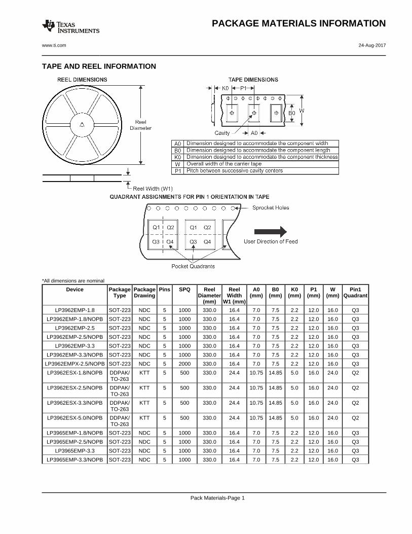
TAPE AND REEL INFORMATION
*All dimensions are nominal
Device PackageType
PackageDrawing
Pins SPQ ReelDiameter
(mm)
ReelWidth
W1 (mm)
A0(mm)
B0(mm)
K0(mm)
P1(mm)
W(mm)
Pin1Quadrant
LP3962EMP-1.8 SOT-223 NDC 5 1000 330.0 16.4 7.0 7.5 2.2 12.0 16.0 Q3
LP3962EMP-1.8/NOPB SOT-223 NDC 5 1000 330.0 16.4 7.0 7.5 2.2 12.0 16.0 Q3
LP3962EMP-2.5 SOT-223 NDC 5 1000 330.0 16.4 7.0 7.5 2.2 12.0 16.0 Q3
LP3962EMP-2.5/NOPB SOT-223 NDC 5 1000 330.0 16.4 7.0 7.5 2.2 12.0 16.0 Q3
LP3962EMP-3.3 SOT-223 NDC 5 1000 330.0 16.4 7.0 7.5 2.2 12.0 16.0 Q3
LP3962EMP-3.3/NOPB SOT-223 NDC 5 1000 330.0 16.4 7.0 7.5 2.2 12.0 16.0 Q3
LP3962EMPX-2.5/NOPB SOT-223 NDC 5 2000 330.0 16.4 7.0 7.5 2.2 12.0 16.0 Q3
LP3962ESX-1.8/NOPB DDPAK/TO-263
KTT 5 500 330.0 24.4 10.75 14.85 5.0 16.0 24.0 Q2
LP3962ESX-2.5/NOPB DDPAK/TO-263
KTT 5 500 330.0 24.4 10.75 14.85 5.0 16.0 24.0 Q2
LP3962ESX-3.3/NOPB DDPAK/TO-263
KTT 5 500 330.0 24.4 10.75 14.85 5.0 16.0 24.0 Q2
LP3962ESX-5.0/NOPB DDPAK/TO-263
KTT 5 500 330.0 24.4 10.75 14.85 5.0 16.0 24.0 Q2
LP3965EMP-1.8/NOPB SOT-223 NDC 5 1000 330.0 16.4 7.0 7.5 2.2 12.0 16.0 Q3
LP3965EMP-2.5/NOPB SOT-223 NDC 5 1000 330.0 16.4 7.0 7.5 2.2 12.0 16.0 Q3
LP3965EMP-3.3 SOT-223 NDC 5 1000 330.0 16.4 7.0 7.5 2.2 12.0 16.0 Q3
LP3965EMP-3.3/NOPB SOT-223 NDC 5 1000 330.0 16.4 7.0 7.5 2.2 12.0 16.0 Q3
PACKAGE MATERIALS INFORMATION
www.ti.com 24-Aug-2017
Pack Materials-Page 1

Device PackageType
PackageDrawing
Pins SPQ ReelDiameter
(mm)
ReelWidth
W1 (mm)
A0(mm)
B0(mm)
K0(mm)
P1(mm)
W(mm)
Pin1Quadrant
LP3965EMP-ADJ SOT-223 NDC 5 1000 330.0 16.4 7.0 7.5 2.2 12.0 16.0 Q3
LP3965EMP-ADJ/NOPB SOT-223 NDC 5 1000 330.0 16.4 7.0 7.5 2.2 12.0 16.0 Q3
LP3965EMPX-ADJ/NOPB SOT-223 NDC 5 2000 330.0 16.4 7.0 7.5 2.2 12.0 16.0 Q3
LP3965ESX-1.8/NOPB DDPAK/TO-263
KTT 5 500 330.0 24.4 10.75 14.85 5.0 16.0 24.0 Q2
LP3965ESX-2.5/NOPB DDPAK/TO-263
KTT 5 500 330.0 24.4 10.75 14.85 5.0 16.0 24.0 Q2
LP3965ESX-3.3 DDPAK/TO-263
KTT 5 500 330.0 24.4 10.75 14.85 5.0 16.0 24.0 Q2
LP3965ESX-3.3/NOPB DDPAK/TO-263
KTT 5 500 330.0 24.4 10.75 14.85 5.0 16.0 24.0 Q2
LP3965ESX-ADJ/NOPB DDPAK/TO-263
KTT 5 500 330.0 24.4 10.75 14.85 5.0 16.0 24.0 Q2
*All dimensions are nominal
Device Package Type Package Drawing Pins SPQ Length (mm) Width (mm) Height (mm)
LP3962EMP-1.8 SOT-223 NDC 5 1000 367.0 367.0 35.0
LP3962EMP-1.8/NOPB SOT-223 NDC 5 1000 367.0 367.0 35.0
LP3962EMP-2.5 SOT-223 NDC 5 1000 367.0 367.0 35.0
LP3962EMP-2.5/NOPB SOT-223 NDC 5 1000 367.0 367.0 35.0
LP3962EMP-3.3 SOT-223 NDC 5 1000 367.0 367.0 35.0
PACKAGE MATERIALS INFORMATION
www.ti.com 24-Aug-2017
Pack Materials-Page 2

Device Package Type Package Drawing Pins SPQ Length (mm) Width (mm) Height (mm)
LP3962EMP-3.3/NOPB SOT-223 NDC 5 1000 367.0 367.0 35.0
LP3962EMPX-2.5/NOPB SOT-223 NDC 5 2000 367.0 367.0 35.0
LP3962ESX-1.8/NOPB DDPAK/TO-263 KTT 5 500 367.0 367.0 45.0
LP3962ESX-2.5/NOPB DDPAK/TO-263 KTT 5 500 367.0 367.0 45.0
LP3962ESX-3.3/NOPB DDPAK/TO-263 KTT 5 500 367.0 367.0 45.0
LP3962ESX-5.0/NOPB DDPAK/TO-263 KTT 5 500 367.0 367.0 45.0
LP3965EMP-1.8/NOPB SOT-223 NDC 5 1000 367.0 367.0 35.0
LP3965EMP-2.5/NOPB SOT-223 NDC 5 1000 367.0 367.0 35.0
LP3965EMP-3.3 SOT-223 NDC 5 1000 367.0 367.0 35.0
LP3965EMP-3.3/NOPB SOT-223 NDC 5 1000 367.0 367.0 35.0
LP3965EMP-ADJ SOT-223 NDC 5 1000 367.0 367.0 35.0
LP3965EMP-ADJ/NOPB SOT-223 NDC 5 1000 367.0 367.0 35.0
LP3965EMPX-ADJ/NOPB SOT-223 NDC 5 2000 367.0 367.0 35.0
LP3965ESX-1.8/NOPB DDPAK/TO-263 KTT 5 500 367.0 367.0 45.0
LP3965ESX-2.5/NOPB DDPAK/TO-263 KTT 5 500 367.0 367.0 45.0
LP3965ESX-3.3 DDPAK/TO-263 KTT 5 500 367.0 367.0 45.0
LP3965ESX-3.3/NOPB DDPAK/TO-263 KTT 5 500 367.0 367.0 45.0
LP3965ESX-ADJ/NOPB DDPAK/TO-263 KTT 5 500 367.0 367.0 45.0
PACKAGE MATERIALS INFORMATION
www.ti.com 24-Aug-2017
Pack Materials-Page 3
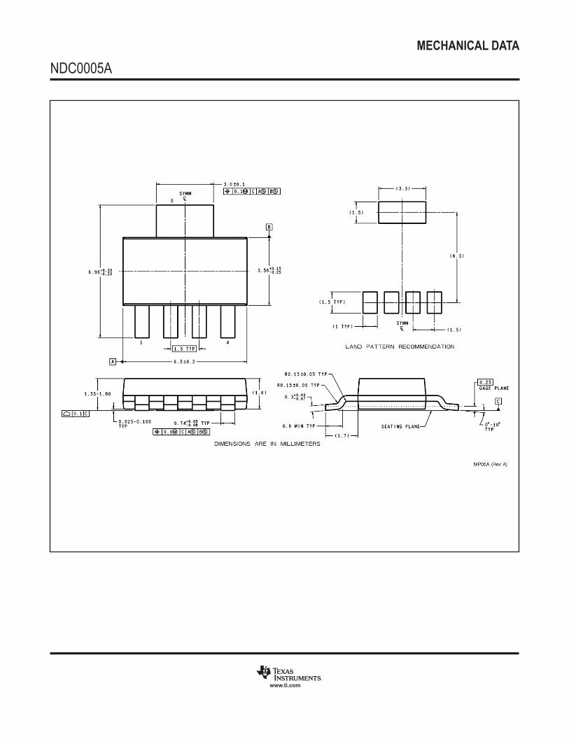
MECHANICAL DATA
NDC0005A
www.ti.com

MECHANICAL DATA
NDH0005D
www.ti.com

MECHANICAL DATA
KTT0005B
www.ti.com
BOTTOM SIDE OF PACKAGE
TS5B (Rev D)

MECHANICAL DATA
NEB0005F
www.ti.com

MECHANICAL DATA
NEB0005B
www.ti.com
IMPORTANT NOTICE
Texas Instruments Incorporated (TI) reserves the right to make corrections, enhancements, improvements and other changes to itssemiconductor products and services per JESD46, latest issue, and to discontinue any product or service per JESD48, latest issue. Buyersshould obtain the latest relevant information before placing orders and should verify that such information is current and complete.TI’s published terms of sale for semiconductor products (http://www.ti.com/sc/docs/stdterms.htm) apply to the sale of packaged integratedcircuit products that TI has qualified and released to market. Additional terms may apply to the use or sale of other types of TI products andservices.Reproduction of significant portions of TI information in TI data sheets is permissible only if reproduction is without alteration and isaccompanied by all associated warranties, conditions, limitations, and notices. TI is not responsible or liable for such reproduceddocumentation. Information of third parties may be subject to additional restrictions. Resale of TI products or services with statementsdifferent from or beyond the parameters stated by TI for that product or service voids all express and any implied warranties for theassociated TI product or service and is an unfair and deceptive business practice. TI is not responsible or liable for any such statements.Buyers and others who are developing systems that incorporate TI products (collectively, “Designers”) understand and agree that Designersremain responsible for using their independent analysis, evaluation and judgment in designing their applications and that Designers havefull and exclusive responsibility to assure the safety of Designers' applications and compliance of their applications (and of all TI productsused in or for Designers’ applications) with all applicable regulations, laws and other applicable requirements. Designer represents that, withrespect to their applications, Designer has all the necessary expertise to create and implement safeguards that (1) anticipate dangerousconsequences of failures, (2) monitor failures and their consequences, and (3) lessen the likelihood of failures that might cause harm andtake appropriate actions. Designer agrees that prior to using or distributing any applications that include TI products, Designer willthoroughly test such applications and the functionality of such TI products as used in such applications.TI’s provision of technical, application or other design advice, quality characterization, reliability data or other services or information,including, but not limited to, reference designs and materials relating to evaluation modules, (collectively, “TI Resources”) are intended toassist designers who are developing applications that incorporate TI products; by downloading, accessing or using TI Resources in anyway, Designer (individually or, if Designer is acting on behalf of a company, Designer’s company) agrees to use any particular TI Resourcesolely for this purpose and subject to the terms of this Notice.TI’s provision of TI Resources does not expand or otherwise alter TI’s applicable published warranties or warranty disclaimers for TIproducts, and no additional obligations or liabilities arise from TI providing such TI Resources. TI reserves the right to make corrections,enhancements, improvements and other changes to its TI Resources. TI has not conducted any testing other than that specificallydescribed in the published documentation for a particular TI Resource.Designer is authorized to use, copy and modify any individual TI Resource only in connection with the development of applications thatinclude the TI product(s) identified in such TI Resource. NO OTHER LICENSE, EXPRESS OR IMPLIED, BY ESTOPPEL OR OTHERWISETO ANY OTHER TI INTELLECTUAL PROPERTY RIGHT, AND NO LICENSE TO ANY TECHNOLOGY OR INTELLECTUAL PROPERTYRIGHT OF TI OR ANY THIRD PARTY IS GRANTED HEREIN, including but not limited to any patent right, copyright, mask work right, orother intellectual property right relating to any combination, machine, or process in which TI products or services are used. Informationregarding or referencing third-party products or services does not constitute a license to use such products or services, or a warranty orendorsement thereof. Use of TI Resources may require a license from a third party under the patents or other intellectual property of thethird party, or a license from TI under the patents or other intellectual property of TI.TI RESOURCES ARE PROVIDED “AS IS” AND WITH ALL FAULTS. TI DISCLAIMS ALL OTHER WARRANTIES ORREPRESENTATIONS, EXPRESS OR IMPLIED, REGARDING RESOURCES OR USE THEREOF, INCLUDING BUT NOT LIMITED TOACCURACY OR COMPLETENESS, TITLE, ANY EPIDEMIC FAILURE WARRANTY AND ANY IMPLIED WARRANTIES OFMERCHANTABILITY, FITNESS FOR A PARTICULAR PURPOSE, AND NON-INFRINGEMENT OF ANY THIRD PARTY INTELLECTUALPROPERTY RIGHTS. TI SHALL NOT BE LIABLE FOR AND SHALL NOT DEFEND OR INDEMNIFY DESIGNER AGAINST ANY CLAIM,INCLUDING BUT NOT LIMITED TO ANY INFRINGEMENT CLAIM THAT RELATES TO OR IS BASED ON ANY COMBINATION OFPRODUCTS EVEN IF DESCRIBED IN TI RESOURCES OR OTHERWISE. IN NO EVENT SHALL TI BE LIABLE FOR ANY ACTUAL,DIRECT, SPECIAL, COLLATERAL, INDIRECT, PUNITIVE, INCIDENTAL, CONSEQUENTIAL OR EXEMPLARY DAMAGES INCONNECTION WITH OR ARISING OUT OF TI RESOURCES OR USE THEREOF, AND REGARDLESS OF WHETHER TI HAS BEENADVISED OF THE POSSIBILITY OF SUCH DAMAGES.Unless TI has explicitly designated an individual product as meeting the requirements of a particular industry standard (e.g., ISO/TS 16949and ISO 26262), TI is not responsible for any failure to meet such industry standard requirements.Where TI specifically promotes products as facilitating functional safety or as compliant with industry functional safety standards, suchproducts are intended to help enable customers to design and create their own applications that meet applicable functional safety standardsand requirements. Using products in an application does not by itself establish any safety features in the application. Designers mustensure compliance with safety-related requirements and standards applicable to their applications. Designer may not use any TI products inlife-critical medical equipment unless authorized officers of the parties have executed a special contract specifically governing such use.Life-critical medical equipment is medical equipment where failure of such equipment would cause serious bodily injury or death (e.g., lifesupport, pacemakers, defibrillators, heart pumps, neurostimulators, and implantables). Such equipment includes, without limitation, allmedical devices identified by the U.S. Food and Drug Administration as Class III devices and equivalent classifications outside the U.S.TI may expressly designate certain products as completing a particular qualification (e.g., Q100, Military Grade, or Enhanced Product).Designers agree that it has the necessary expertise to select the product with the appropriate qualification designation for their applicationsand that proper product selection is at Designers’ own risk. Designers are solely responsible for compliance with all legal and regulatoryrequirements in connection with such selection.Designer will fully indemnify TI and its representatives against any damages, costs, losses, and/or liabilities arising out of Designer’s non-compliance with the terms and provisions of this Notice.
Mailing Address: Texas Instruments, Post Office Box 655303, Dallas, Texas 75265Copyright © 2017, Texas Instruments Incorporated