Embed Size (px)
Citation preview
C
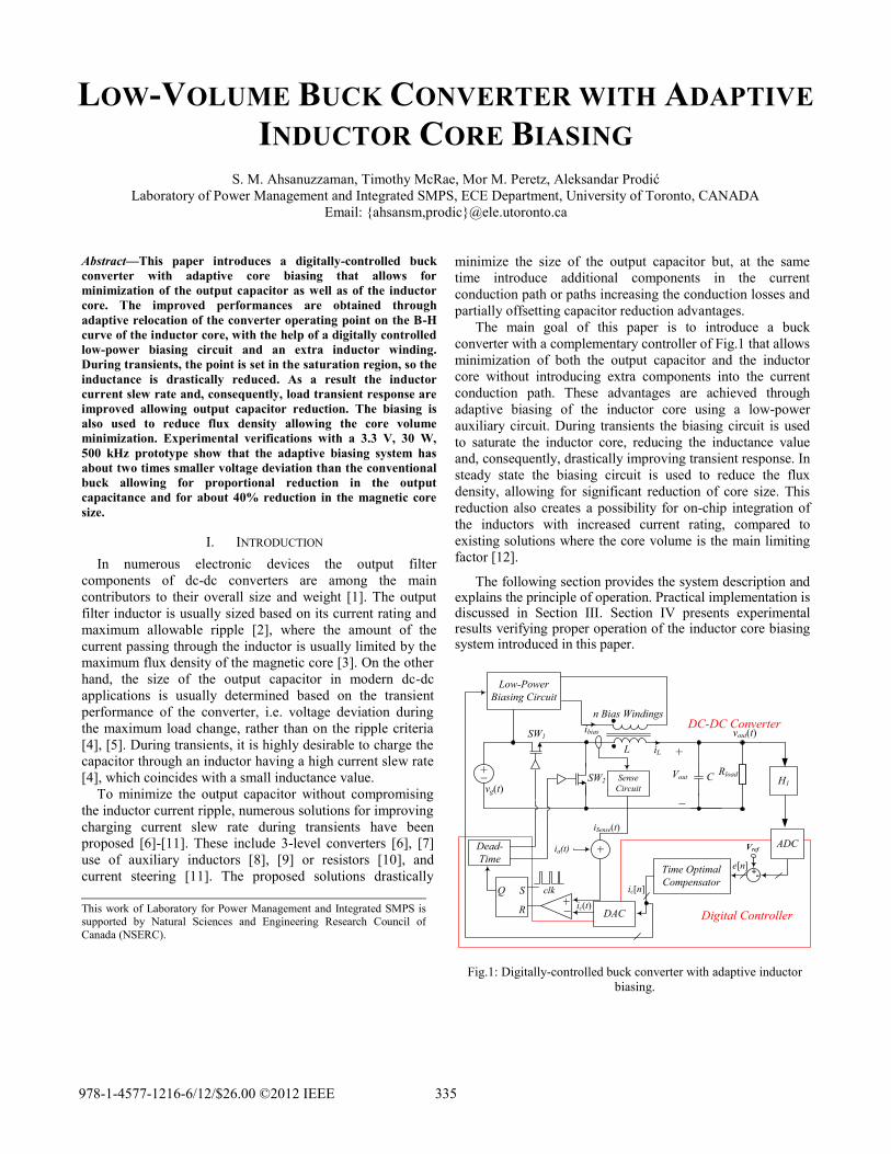
+
vout(t)
Rload
vg(t)
L
_
+_SW2
DC-DC Converter
Time Optimal
Compensator
iSense(t)
VoutSense
Circuit
SW1
H1
ADC
+-e[n]
Vref
DAC+_
S
R
Q
Dead-
Time
Digital Controller
ic[n]
ic(t)
clk
+ia(t)
Low-Power
Biasing Circuit
n Bias Windings
ibias
iL
Fig.1: Digitally-controlled buck converter with adaptive inductor
biasing.
LOW-VOLUME BUCK CONVERTER WITH ADAPTIVE
INDUCTOR CORE BIASING
S. M. Ahsanuzzaman, Timothy McRae, Mor M. Peretz, Aleksandar Prodić
Laboratory of Power Management and Integrated SMPS, ECE Department, University of Toronto, CANADA
Email: {ahsansm,prodic}@ele.utoronto.ca
Abstract—This paper introduces a digitally-controlled buck
converter with adaptive core biasing that allows for
minimization of the output capacitor as well as of the inductor
core. The improved performances are obtained through
adaptive relocation of the converter operating point on the B-H
curve of the inductor core, with the help of a digitally controlled
low-power biasing circuit and an extra inductor winding.
During transients, the point is set in the saturation region, so the
inductance is drastically reduced. As a result the inductor
current slew rate and, consequently, load transient response are
improved allowing output capacitor reduction. The biasing is
also used to reduce flux density allowing the core volume
minimization. Experimental verifications with a 3.3 V, 30 W,
500 kHz prototype show that the adaptive biasing system has
about two times smaller voltage deviation than the conventional
buck allowing for proportional reduction in the output
capacitance and for about 40% reduction in the magnetic core
size.
I. INTRODUCTION
In numerous electronic devices the output filter
components of dc-dc converters are among the main
contributors to their overall size and weight [1]. The output
filter inductor is usually sized based on its current rating and
maximum allowable ripple [2], where the amount of the
current passing through the inductor is usually limited by the
maximum flux density of the magnetic core [3]. On the other
hand, the size of the output capacitor in modern dc-dc
applications is usually determined based on the transient
performance of the converter, i.e. voltage deviation during
the maximum load change, rather than on the ripple criteria
[4], [5]. During transients, it is highly desirable to charge the
capacitor through an inductor having a high current slew rate
[4], which coincides with a small inductance value.
To minimize the output capacitor without compromising
the inductor current ripple, numerous solutions for improving
charging current slew rate during transients have been
proposed [6]-[11]. These include 3-level converters [6], [7]
use of auxiliary inductors [8], [9] or resistors [10], and
current steering [11]. The proposed solutions drastically
minimize the size of the output capacitor but, at the same
time introduce additional components in the current
conduction path or paths increasing the conduction losses and
partially offsetting capacitor reduction advantages.
The main goal of this paper is to introduce a buck
converter with a complementary controller of Fig.1 that allows
minimization of both the output capacitor and the inductor
core without introducing extra components into the current
conduction path. These advantages are achieved through
adaptive biasing of the inductor core using a low-power
auxiliary circuit. During transients the biasing circuit is used
to saturate the inductor core, reducing the inductance value
and, consequently, drastically improving transient response. In
steady state the biasing circuit is used to reduce the flux
density, allowing for significant reduction of core size. This
reduction also creates a possibility for on-chip integration of
the inductors with increased current rating, compared to
existing solutions where the core volume is the main limiting
factor [12].
The following section provides the system description and explains the principle of operation. Practical implementation is discussed in Section III. Section IV presents experimental results verifying proper operation of the inductor core biasing system introduced in this paper.
This work of Laboratory for Power Management and Integrated SMPS is supported by Natural Sciences and Engineering Research Council of
Canada (NSERC).
978-1-4577-1216-6/12/$26.00 ©2012 IEEE 335

µL
Light to
heavy
transient
Light load H (A/m)
B (T) Heavy Load
Heavy to
light
transient
∆iL
Inductor Current
A
(Vg-Vout)/L
N.∆iL/lcore
Fig.2 (a) Inductor current of a conventional buck during a light-
to-heavy load transient. (b) Corresponding B-H curve with load
transient trajectories; where L is inductance, lcore is core length,
N is number of turns in the winding and ∆iL is the change of load
current.
Biasing at light
load
Heavy load
Biasing at heavy
load
Heavy to light
transient
H (A/m)
B (T)
Light to heavy
transient
Light load
1
3
2
4
Fig.3. Relocation of the operating point on B-H curve through
adaptive core biasing
II. SYSTEM DESCRIPTION AND PRINCIPLE OF OPERATION
In the conventional design of power converters, the
inductor needs to meet the steady state current ripple
constraint under all operating conditions [2]. The inductor
core is designed such that it stays well below saturation for
the rated maximum current of the converter. This is to
guarantee that the current ripple stays within the constraint
for heavier load conditions.
The approach shown here allows core biasing. The power
supply of Fig.1 is a simple modification of a mixed-signal
current programmed mode (CPM) controlled buck converter
[13], [14]. Here the outer voltage loop is digital and it sets the
current reference for the analog control loop, through a
digital-to-analog converter (DAC). An extra inductor winding
and a low-power biasing circuit are added to the system. The
biasing circuit is controlled by the signal ic[n], which is
inherently available digital equivalent of the inductor current
reference. The voltage loop also contains an analog-to-digital
converter (ADC) and a proximity-time optimal compensator
[15]-[18] that provides recovery from transients in the
virtually fastest possible time, through a single on-off
switching action.
As explained in the following subsections, the bias module
adaptively changes the location of the operating point on the
inductor B-H curve. This allows the core to saturate during
transients, decreasing the inductance value, L and, hence,
improving the transient response. The adaptive biasing also
minimizes the magnetic core by reducing the flux density
inside the core.
A. Light-to-Heavy Load Transient Improvement
To explain the operation of the converter, simplified
inductor B-H curves and inductor current waveform during
transient of Figs.2 and 3 can be used. In conventional
converters, light load operation sets the inductor core well
into the linear region of the B-H curve (point A, Fig.2.b).
During light-to-heavy load transients the rate of change of the
inductor current of the buck converter is limited by:
L
VV
d t
d i outgL
, (1)
where Vg and Vout are the input and output voltages of the
converter, respectively. The inductance, L is proportional to
the slope of the curve around the operating point. As the load
and, consequently, the inductor current increase, the
operating point travels along the B-H curve through the linear
region. During this transient the inductance is mostly constant
and as shown in Fig.2, the inductor slew rate is approximately
the same as in the steady state.
In the system introduced here a biasing winding is used to
adaptively relocate the position of the operating point on the
B-H curve. The adaptive biasing is demonstrated in Fig.3. At
light loads, the operating point is relocated close to the top
knee of the B-H curve (point 1). This relocation allows a
light-to-heavy load transient to push the core into saturation,
i.e. to move from point 1 to 2, drastically reducing the
inductance value. As a result, the inductor current slew rate
is increased and the transient performance improved. The
operating point is relocated by providing a positive dc current
to the biasing winding of the core (Figs. 1 and 4) therefore,
increasing the flux density. Once the transient is completed,
the biasing circuit brings the operating point back to the
linear region (to point 3), where the inductance is larger, to
maintain a low current ripple.
336

Lprimary
n-Bias
Windings Air Gap
ibias_L-to-H
ibias_H-to-L
iL
iL_flux
ibias_flux
ibias_flux
Lbiasing
Fig.4. Simplified diagram of the inductor with biasing
windings
B. Heavy-to-Light Load Transient Improvement
During a heavy-to-light load transient, the inductor current
slew rate of the buck converter is limited by:
L
V
dt
di outL (3)
Similar to the previous operation, at heavy loads the operating point on the B-H curve is relocated to improve the current slew rate and consequently, heavy-to-light load transient response. In this case the biasing circuit brings the operating point close to the bottom knee of the B-H curve (point 3 of Fig.3) so that a sudden drop in the inductor current iL(t) pushes the core into saturation. This moves the operating point from 3 to 4. In this way the inductance value is reduced and the current slew rate is increased. The core stays in this low inductance mode until the optimal controller recovers the voltage. After the transient is completed, the biasing circuit brings the operating point back to the linear region of the B-H curve (point 1), increasing inductance.
C. Ripple Current Reduction using Biasing
In addition to the increase of slew rate and consequent output
capacitor reduction, the biasing also allows inductor core
reduction. As described previously, for heavy loads the
biasing is applied such that a flux of opposite direction from
that created by iL(t) is established. This effectively means that
the net flux through the core, i.e. flux density, is reduced and
that the cross-sectional area of the core can be reduced as
well. As it is shown in the experimental section of this paper,
the biasing allows up to 40% reduction in the core size
depending on the core geometry. This feature is well suited
for on-chip integration of the inductors with semiconductor
components of low-power supplies where the limited
dimension of the magnetic materials is among the main
obstacles in increasing the current rating of the integrated
solutions [12].
III. PRACTICAL IMPLEMENTATION
The key elements of the adaptive biasing converter are the low-power biasing circuit and the inductor with biasing core. In this section their practical implementation is described. The biasing circuit of Fig.5 is designed with having overall system efficiency in mind. To minimize the requirements for the biasing current and, at the same time, maximize its effect on the core flux density, a biasing winding with a significantly larger number of turns than that of the main inductor is used. The biasing current is provided through a structure consisting of a digital-to-analog converter (DAC) and an H-bridge. The DAC operates as a voltage source whose output value is regulated such that the desired biasing current is achieved. The H-bridge is used to change the polarity of the biasing current. As described in the previous section, the polarity of the current depends on the operating conditions and, in this implementation, is changed with the polarity control block. Both the DAC and the polarity control block receive the control signals from the mapping circuit, which transfers the current control loop reference signal ic[n] (Fig.1) into a digital value proportional to the biasing current ibias[n].
A. Inductor with Biasing Winding
As described in the previous subsection, in this implementation a biasing winding with a larger number of turns than that of the main inductor L is used to minimize power consumption. However, if implemented as shown in
DACDACMappingMapping
Polarity controlPolarity control
iL(t)
ibias(t)|vbias(t)|
+
-
c1 c2
c3 c4
c1-c4
ic[n] ibias[n]
n
Fig.5 Low-power biasing circuit
337

1/3 N
turns2/3 N
turns
Lprimary Air Gap
ibias_in
ibias_out
1/3ᵩbias
2/3ᵩbias
iL
ᵩiL
Fig.6. Implementation of the inductor with biasing winding.
Output Voltage
Inductor Current
2.5 A
0 A
100 mV
Fig.7. The light-to-heavy load transient without core biasing–
Ch1: output converter voltage (50mV/div); Ch2: inductor current
(1A/div).
Output voltage
Inductor Current
Biasing
2.5 A
0 A
60 mV
Fig.8. The light-to-heavy load transient with core biasing– Ch1:
output converter voltage (50mV/div); Ch2: inductor current
(1A/div).
Output Voltage
Inductor Current
10 A
1 A
iL-ripple= 5A
Fig.9. 9A load step without core biasing– Ch1: output
converter voltage (100mV/div); Ch2: inductor current
(5A/div).
Fig.4, the larger number of turns can cause a large reflected voltage spike from the main winding affecting the circuit operation. To reduce this problem the inductor is designed so that a partial cancellation of the flux caused by the main inductor winding is achieved. The implementation is shown in Fig.6. The biasing winding is a simple addition to the widely used E-core inductor [19]. Here, the biasing windings are placed across side legs [20], [21] of the core and the main inductor is winded across the centre leg, as in conventional implementations. As shown in Fig.6, the number of turns on the side legs is different and the right leg has twice as many turns. Here the biasing is performed such that during transients the right leg of the core is most saturated. The flux lines also show that, in this configuration the main winding partially cancels the flux of the biasing winding through one leg and contributes to the flux of the other leg, resulting in net reflected voltage that is a 1/3 of the straightforward design
shown in Fig.4. A larger cancellation of the reflected voltage is possible but it comes at the cost of a significant increase in power consumption of the biasing circuit.
IV. EXPERIMENTAL SYSTEM AND RESULTS
Based on diagrams of Figs. 1, 5, and 6, a 10 V - to - 3.3 V,
500 kHz experimental prototype was built. Even though the
maximum inductor current of the adaptive biasing buck is
about 10A, an off-shelf E-core inductor with core saturation at
4A was used. For the controller, an FPGA evaluation board
and discrete components were used. The inductor was
modified by placing biasing winding on the side legs of the
core, as described in the previous section. To verify
advantages of the introduced concept, the performance of the
system with and without influence of the biasing circuit are
compared in Figs.7 and 8. The results show that with the
adaptive biasing transient performance is improved and results
in a 1.6 times smaller output voltage deviation allowing for
equivalent reduction in the output capacitor value. In order to
show the ability to reduce the steady stage current ripple,
hence allowing larger than rated current for the core, a very
large load step (9A) was performed on the same core. As Fig.9
shows this large load step pushes the core deep into saturation,
drastically increasing the ripple compared to light load
operation. Fig.10 shows how the biasing reduces the ripple
back to normal operating condition. As the bias current is
338
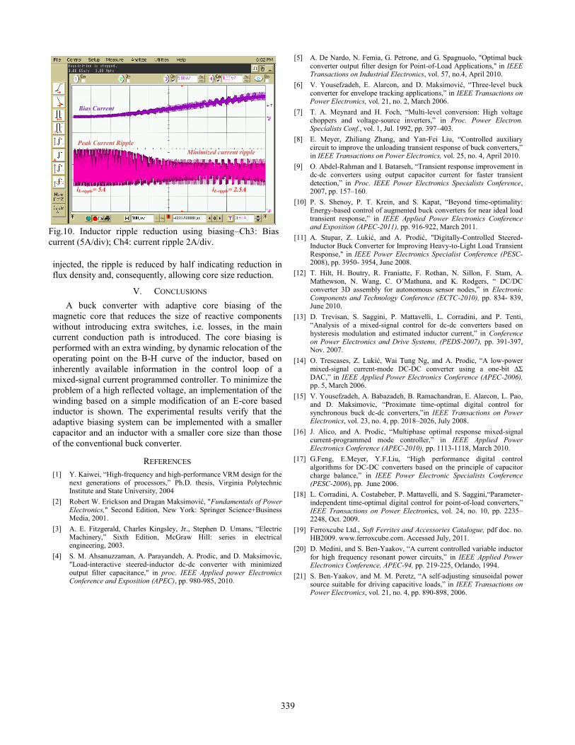
Bias Current
Peak Current Ripple
Minimized current ripple
iL-ripple= 5A iL-ripple= 2.5A
Fig.10. Inductor ripple reduction using biasing–Ch3: Bias
current (5A/div); Ch4: current ripple 2A/div.
injected, the ripple is reduced by half indicating reduction in
flux density and, consequently, allowing core size reduction.
V. CONCLUSIONS
A buck converter with adaptive core biasing of the
magnetic core that reduces the size of reactive components
without introducing extra switches, i.e. losses, in the main
current conduction path is introduced. The core biasing is
performed with an extra winding, by dynamic relocation of the
operating point on the B-H curve of the inductor, based on
inherently available information in the control loop of a
mixed-signal current programmed controller. To minimize the
problem of a high reflected voltage, an implementation of the
winding based on a simple modification of an E-core based
inductor is shown. The experimental results verify that the
adaptive biasing system can be implemented with a smaller
capacitor and an inductor with a smaller core size than those
of the conventional buck converter.
REFERENCES
[1] Y. Kaiwei, “High-frequency and high-performance VRM design for the next generations of processors,” Ph.D. thesis, Virginia Polytechnic Institute and State University, 2004
[2] Robert W. Erickson and Dragan Maksimović, "Fundamentals of Power Electronics," Second Edition, New York: Springer Science+Business Media, 2001.
[3] A. E. Fitzgerald, Charles Kingsley, Jr., Stephen D. Umans, “Electric Machinery,” Sixth Edition, McGraw Hill: series in electrical engineering, 2003.
[4] S. M. Ahsanuzzaman, A. Parayandeh, A. Prodic, and D. Maksimovic, "Load-interactive steered-inductor dc-dc converter with minimized output filter capacitance," in proc. IEEE Applied power Electronics Conference and Exposition (APEC), pp. 980-985, 2010.
[5] A. De Nardo, N. Femia, G. Petrone, and G. Spagnuolo, "Optimal buck converter output filter design for Point-of-Load Applications," in IEEE Transactions on Industrial Electronics, vol. 57, no.4, April 2010.
[6] V. Yousefzadeh, E. Alarcon, and D. Maksimović, “Three-level buck converter for envelope tracking applications,” in IEEE Transactions on Power Electronics, vol. 21, no. 2, March 2006.
[7] T. A. Meynard and H. Foch, “Multi-level conversion: High voltage choppers and voltage-source inverters,” in Proc. Power Electron. Specialists Conf., vol. 1, Jul. 1992, pp. 397–403.
[8] E. Meyer, Zhiliang Zhang, and Yan-Fei Liu, “Controlled auxiliary circuit to improve the unloading transient response of buck converters,” in IEEE Transactions on Power Electronics, vol. 25, no. 4, April 2010.
[9] O. Abdel-Rahman and I. Batarseh, “Transient response improvement in dc-dc converters using output capacitor current for faster transient detection,” in Proc. IEEE Power Electronics Specialists Conference, 2007, pp. 157–160.
[10] P. S. Shenoy, P. T. Krein, and S. Kapat, “Beyond time-optimality: Energy-based control of augmented buck converters for near ideal load transient response,” in IEEE Applied Power Electronics Conference and Exposition (APEC-2011), pp. 916-922, March 2011.
[11] A. Stupar, Z. Lukić, and A. Prodić, "Digitally-Controlled Steered- Inductor Buck Converter for Improving Heavy-to-Light Load Transient Response," in IEEE Power Electronics Specialist Conference (PESC- 2008), pp. 3950- 3954, June 2008.
[12] T. Hilt, H. Boutry, R. Franiatte, F. Rothan, N. Sillon, F. Stam, A. Mathewson, N. Wang, C. O’Mathuna, and K. Rodgers, “ DC/DC converter 3D assembly for autonomous sensor nodes,” in Electronic Components and Technology Conference (ECTC-2010), pp. 834- 839, June 2010.
[13] D. Trevisan, S. Saggini, P. Mattavelli, L. Corradini, and P. Tenti, “Analysis of a mixed-signal control for dc-dc converters based on hysteresis modulation and estimated inductor current,” in Conference on Power Electronics and Drive Systems, (PEDS-2007), pp. 391-397, Nov. 2007.
[14] O. Trescases, Z. Lukić, Wai Tung Ng, and A. Prodic, “A low-power mixed-signal current-mode DC-DC converter using a one-bit ∆Σ DAC,” in IEEE Applied Power Electronics Conference (APEC-2006), pp. 5, March 2006.
[15] V. Yousefzadeh, A. Babazadeh, B. Ramachandran, E. Alarcon, L. Pao, and D. Maksimovic, “Proximate time-optimal digital control for synchronous buck dc-dc converters,”in IEEE Transactions on Power Electronics, vol. 23, no. 4, pp. 2018–2026, July 2008.
[16] J. Alico, and A. Prodic, “Multiphase optimal response mixed-signal current-programmed mode controller,” in IEEE Applied Power Electronics Conference (APEC-2010), pp. 1113-1118, March 2010.
[17] G.Feng, E.Meyer, Y.F.Liu, “High performance digital control algorithms for DC-DC converters based on the principle of capacitor charge balance,” in IEEE Power Electronic Specialists Conference (PESC-2006), pp. June 2006.
[18] L. Corradini, A. Costabeber, P. Mattavelli, and S. Saggini,“Parameter-independent time-optimal digital control for point-of-load converters,” IEEE Transactions on Power Electronics, vol. 24, no. 10, pp. 2235– 2248, Oct. 2009.
[19] Ferroxcube Ltd., Soft Ferrites and Accessories Catalogue, pdf doc. no. HB2009. www.ferroxcube.com. Accessed July, 2011.
[20] D. Medini, and S. Ben-Yaakov, “A current controlled variable inductor for high frequency resonant power circuits,” in IEEE Applied Power Electronics Conference, APEC-94, pp. 219-225, Orlando, 1994.
[21] S. Ben-Yaakov, and M. M. Peretz, “A self-adjusting sinusoidal power source suitable for driving capacitive loads,” in IEEE Transactions on Power Electronics, vol. 21, no. 4, pp. 890-898, 2006.
339