Embed Size (px)
Citation preview
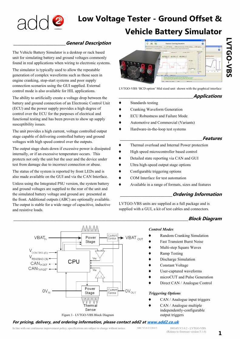
Low Voltage Tester - Ground Offset &
Vehicle Battery Simulator
1
LV
TG
O-V
BS
In line with our continuous improvement policy, specifications are subject to change without notice. J001451V3.0.2 - LVTGO-VBS SBC/V3.0.2/120413
(Relates to firmware version 5.1.0)
__________________________General Description
The Vehicle Battery Simulator is a desktop or rack based
unit for simulating battery and ground voltages commonly
found in real applications when wiring to electronic systems.
The simulator is typically used to allow the repeatable
generation of complex waveforms such as those seen in
engine cranking, stop-start systems and poor supply
connection scenarios using the GUI supplied. External
control mode is also available for HIL applications.
The ability to artificially create a voltage drop between the
battery and ground connection of an Electronic Control Unit
(ECU) and the power supply provides a high degree of
control over the ECU for the purposes of electrical and
functional testing and has been proven to show up supply
susceptibility issues.
The unit provides a high current, voltage controlled output
stage capable of delivering controlled battery and ground
voltages with high speed control over the outputs.
The output stage shuts down if excessive power is dissipated
internally, or if an excessive temperature occurs. This
protects not only the unit but the user and the device under
test from damage due to incorrect connection or abuse.
The status of the system is reported by front LEDs and is
also made available on the GUI and via the CAN Interface.
Unless using the Integrated PSU version, the system battery
and ground voltages are supplied to the rear of the unit and
the simulated battery voltage and ground are presented at
the front. Additional outputs (ABC) are optionally available.
The output is stable for a wide range of capacitive, inductive
and resistive loads.
_________________________________________Features
Thermal overload and Internal Power protection
High speed microcontroller based control
Detailed state reporting via CAN and GUI
Ultra high-speed output stage options
Configurable triggering options
COM Interface for test automation
Available in a range of formats, sizes and features
__________________________Ordering Information
LVTGO-VBS units are supplied as a full package and is
supplied with a GUI, a kit of test cables and connectors.
_______________________________________________________________________________________Block Diagram
For pricing, delivery, and ordering information, please contact add2 at www.add2.co.uk
Triggering Options
CAN / Analogue input triggers
CAN / Analogue multiple
independently-configurable
output triggers Figure 1– LVTGO-VBS Block Diagram
_____________________________________Applications
Standards testing
Cranking Waveform Generation
ECU Robustness and Failure Mode
Automotive and Commercial (Variants)
Hardware-in-the-loop test systems
LVTGO-VBS ‘BCD option’ Mid sized unit shown with the graphical interface
Control Modes
Random Cranking Simulation
Fast Transient Burst Noise
Multi-step Square Waves
Ramp Testing
Discharge Simulation
Constant Voltage
User-captured waveforms
microCUT and Pulse Generation
Direct CAN / Analogue Control
Low Voltage Tester - Ground Offset &
Vehicle Battery Simulator
2
LV
TG
O-V
BS
In line with our continuous improvement policy, specifications are subject to change without notice. J001451V3.0.2 - LVTGO-VBS SBC/V3.0.2/120413
(Relates to firmware version 5.1.0)
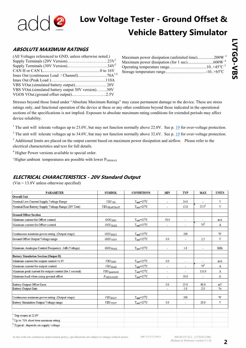
ABSOLUTE MAXIMUM RATINGS
(All Voltages referenced to GND, unless otherwise noted.)
Supply Terminals (20V Version)……………...…………23V1
Supply Terminals (30V Version)...……………………....34V2
CAN H or CAN L.......................................................0 to 16V
Imax Out (continuous Load / Channel)............................70A3 4
Imax Out (Peak Load )…….............................................110A
VBS VOut.(simulated battery output).…………………. 20V
VBS VOut.(simulated battery output 30V version)……..30V
VGOS VOut.(ground offset output)...….……………….2.5V
Stresses beyond those listed under “Absolute Maximum Ratings” may cause permanent damage to the device. These are stress
ratings only, and functional operation of the device at these or any other conditions beyond those indicated in the operational
sections of the specifications is not implied. Exposure to absolute maximum rating conditions for extended periods may affect
device reliability.
1 The unit will tolerate voltages up to 23.0V, but may not function normally above 22.0V. See p. 19 for over-voltage protection.
2 The unit will tolerate voltages up to 34.0V, but may not function normally above 32.6V. See p. 19 for over-voltage protection.
3 Additional limits are placed on the output current based on maximum power dissipation and airflow. Please refer to the
electrical characteristics and text for full details.
4 Higher Power versions available to special order.
5 Higher ambient temperatures are possible with lower PDISMAX
Maximum power dissipation (unlimited time)................200W 4
Maximum power dissipation (for 1 sec).........................600W 4
Operating temperature range....................................10..+45oC 5
Storage temperature range.......................................-10..+65oC
ELECTRICAL CHARACTERISTICS - 20V Standard Output (Vin = 13.8V unless otherwise specified)
Low Voltage Tester - Ground Offset &
Vehicle Battery Simulator
3
LV
TG
O-V
BS
In line with our continuous improvement policy, specifications are subject to change without notice. J001451V3.0.2 - LVTGO-VBS SBC/V3.0.2/120413
(Relates to firmware version 5.1.0)
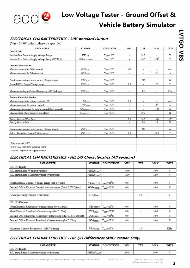
ELECTRICAL CHARACTERISTICS - 30V standard Output (Vin = 24.0V unless otherwise specified)
ELECTRICAL CHARACTERISTICS - HIL I/O Characteristics (All versions)
ELECTRICAL CHARACTERISTICS - HIL I/O Differences (MK2 version Only)
Low Voltage Tester - Ground Offset &
Vehicle Battery Simulator
4
LV
TG
O-V
BS
In line with our continuous improvement policy, specifications are subject to change without notice. J001451V3.0.2 - LVTGO-VBS SBC/V3.0.2/120413
(Relates to firmware version 5.1.0)
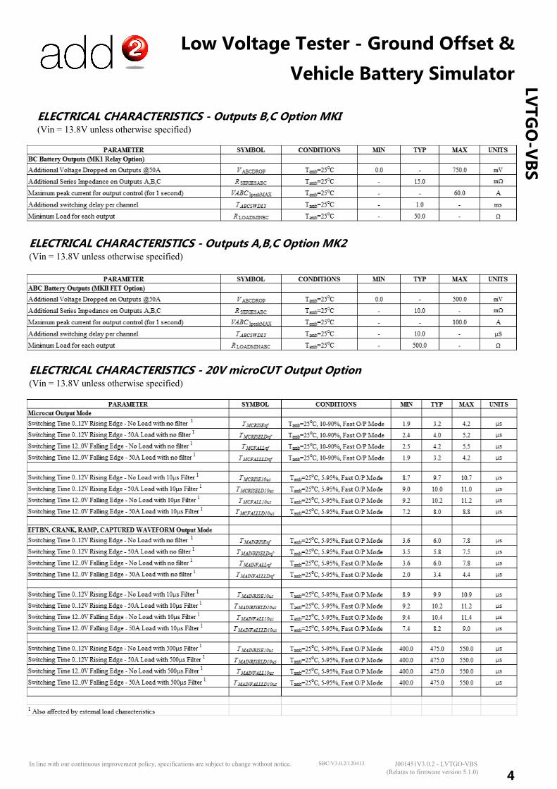
ELECTRICAL CHARACTERISTICS - 20V microCUT Output Option (Vin = 13.8V unless otherwise specified)
ELECTRICAL CHARACTERISTICS - Outputs A,B,C Option MK2 (Vin = 13.8V unless otherwise specified)
ELECTRICAL CHARACTERISTICS - Outputs B,C Option MKI (Vin = 13.8V unless otherwise specified)
Low Voltage Tester - Ground Offset &
Vehicle Battery Simulator
5
LV
TG
O-V
BS
In line with our continuous improvement policy, specifications are subject to change without notice. J001451V3.0.2 - LVTGO-VBS SBC/V3.0.2/120413
(Relates to firmware version 5.1.0)
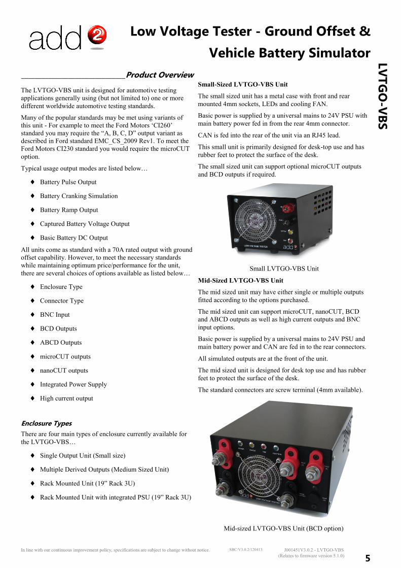
_______________________________Product Overview
The LVTGO-VBS unit is designed for automotive testing
applications generally using (but not limited to) one or more
different worldwide automotive testing standards.
Many of the popular standards may be met using variants of
this unit - For example to meet the Ford Motors ‘CI260’
standard you may require the “A, B, C, D” output variant as
described in Ford standard EMC_CS_2009 Rev1. To meet the
Ford Motors CI230 standard you would require the microCUT
option.
Typical usage output modes are listed below…
Battery Pulse Output
Battery Cranking Simulation
Battery Ramp Output
Captured Battery Voltage Output
Basic Battery DC Output
All units come as standard with a 70A rated output with ground
offset capability. However, to meet the necessary standards
while maintaining optimum price/performance for the unit,
there are several choices of options available as listed below…
Enclosure Type
Connector Type
BNC Input
BCD Outputs
ABCD Outputs
microCUT outputs
nanoCUT outputs
Integrated Power Supply
High current output
Enclosure Types
There are four main types of enclosure currently available for
the LVTGO-VBS…
Single Output Unit (Small size)
Multiple Derived Outputs (Medium Sized Unit)
Rack Mounted Unit (19” Rack 3U)
Rack Mounted Unit with integrated PSU (19” Rack 3U)
Small-Sized LVTGO-VBS Unit
The small sized unit has a metal case with front and rear
mounted 4mm sockets, LEDs and cooling FAN.
Basic power is supplied by a universal mains to 24V PSU with
main battery power fed in from the rear 4mm connector.
CAN is fed into the rear of the unit via an RJ45 lead.
This small unit is primarily designed for desk-top use and has
rubber feet to protect the surface of the desk.
The small sized unit can support optional microCUT outputs
and BCD outputs if required.
Small LVTGO-VBS Unit
Mid-Sized LVTGO-VBS Unit
The mid sized unit may have either single or multiple outputs
fitted according to the options purchased.
The mid sized unit can support microCUT, nanoCUT, BCD
and ABCD outputs as well as high current outputs and BNC
input options.
Basic power is supplied by a universal mains to 24V PSU and
main battery power and CAN are fed in to the rear connectors.
All simulated outputs are at the front of the unit.
The mid sized unit is designed for desk top use and has rubber
feet to protect the surface of the desk.
The standard connectors are screw terminal (4mm available).
Mid-sized LVTGO-VBS Unit (BCD option)
Low Voltage Tester - Ground Offset &
Vehicle Battery Simulator
6
LV
TG
O-V
BS
In line with our continuous improvement policy, specifications are subject to change without notice. J001451V3.0.2 - LVTGO-VBS SBC/V3.0.2/120413
(Relates to firmware version 5.1.0)
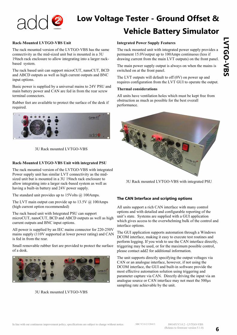
Rack-Mounted LVTGO-VBS Unit
The rack mounted version of the LVTGO-VBS has the same
connectivity as the mid-sized unit but is mounted in a 3U
19inch rack enclosure to allow integrating into a larger rack-
based system.
The rack based unit can support microCUT, nanoCUT, BCD
and ABCD outputs as well as high current outputs and BNC
input options.
Basic power is supplied by a universal mains to 24V PSU and
main battery power and CAN are fed in from the rear screw
terminal connectors.
Rubber feet are available to protect the surface of the desk if
required.
3U Rack mounted LVTGO-VBS
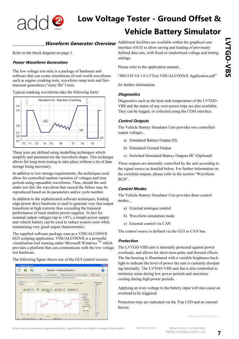
Rack-Mounted LVTGO-VBS Unit with integrated PSU
The rack mounted version of the LVTGO-VBS with integrated
Power supply unit has similar LVT connectivity as the mid-
sized unit but is mounted in a 3U 19inch rack enclosure to
allow integrating into a larger rack-based system as well as
having a built-in battery and 24V power supply.
The standard unit provides up to 15Volts @ 100Amps.
The LVT main output can provide up to 13.5V @ 100Amps
(high current option recommended)
The rack based unit with Integrated PSU can support
microCUT, nanoCUT, BCD and ABCD outputs as well as high
current outputs and BNC input options.
All power is supplied by an IEC mains connector for 220-250V
mains supply (110V supported at lower power rating) and CAN
is fed in from the rear.
Small removable rubber feet are provided to protect the surface
of a desk.
3U Rack mounted LVTGO-VBS
Integrated Power Supply Features
The rack mounted unit with integrated power supply provides a
permanent 15.0Voutput up to 100Amps continuous (less if
drawing current from the main LVT outputs) on the front panel.
The main power supply output is always on when the mains is
switched on at the front panel.
The LVT outputs will default to off (0V) on power up and
requires configuration from the LVT GUI to operate the output.
Thermal considerations
All units have ventilation holes which must be kept free from
obstruction as much as possible for the best overall
performance.
3U Rack mounted LVTGO-VBS with integrated PSU
The CAN Interface and scripting options
All units support a rich CAN interface with many control
options and with detailed and configurable reporting of the
unit’s state. Systems are supplied with a GUI application
which gives access to the overwhelming bulk of the control and
interface options.
The GUI application supports automation through a Windows
DCOM interface, making it easy to execute test routines and
perform logging. If you wish to use the CAN interface directly,
triggering may be used, or for the maximum possible control,
please contact add2 for additional information.
The unit supports directly specifying the output voltages via
CAN or an analogue interface, however, if not using the
DCOM interface, the GUI and built-in software provide the
most effective automation solution using triggering and
parameter capture via CAN. Directly driving the input via an
analogue source or CAN interface may not meet the 500µs
sampling rate achievable by the unit.
Low Voltage Tester - Ground Offset &
Vehicle Battery Simulator
7
LV
TG
O-V
BS
In line with our continuous improvement policy, specifications are subject to change without notice. J001451V3.0.2 - LVTGO-VBS SBC/V3.0.2/120413
(Relates to firmware version 5.1.0)
________________Waveform Generator Overview
Refer to the block diagram on page 1.
Power Waveform Generation
The low voltage test suite is a package of hardware and
software that can create simulations of real-world waveforms
such as engine cranking tests, waveform ramp tests and fast-
transient generation (“rusty file”) tests.
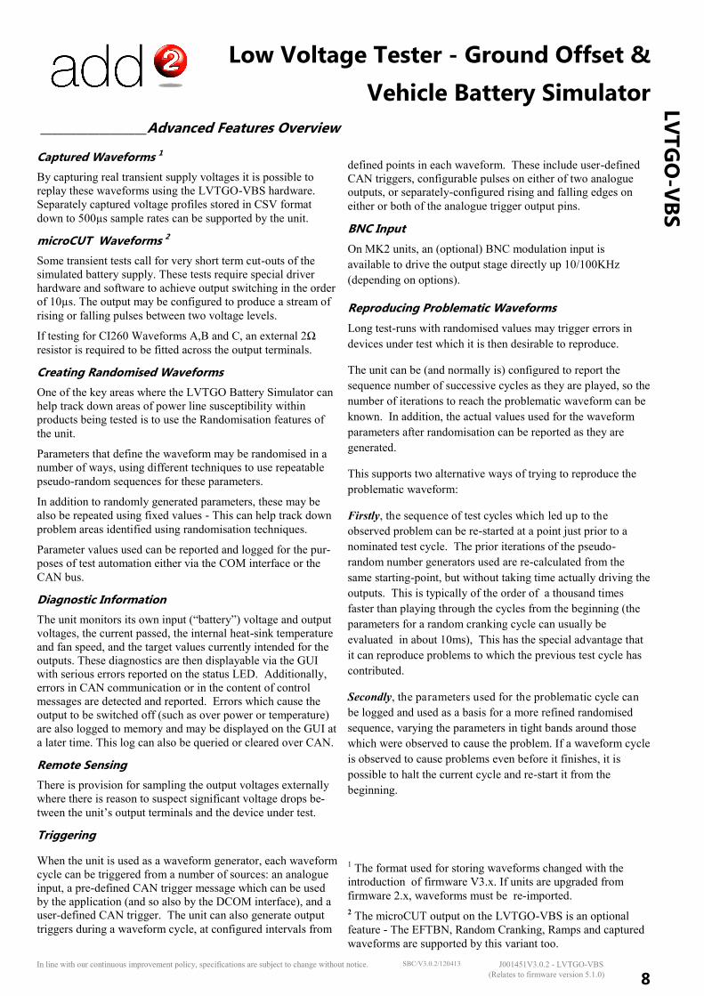
Typical cranking waveforms take the following form:
These tests are defined using modelling techniques which
simplify and parameterize the waveform shape. This technique
allows for long-term testing to take place without a lot of data
storage being necessary.
In addition to low storage requirements, the techniques used
allow for controlled random variation of voltages and time
periods using repeatable waveforms. Thus, should the unit
under test fail, the waveform that caused the failure may be
reproduced based on its parameters and/or cycle number.
In addition to the sophisticated software techniques, leading
edge power drive hardware is used to generate very fast output
transitions at high currents thus exceeding the transient
performance of most modern power supplies. In fact for
nominal output voltages (up to 14V), a simple power supply
and vehicle battery can be used to reduce system costs while
maintaining very good output characteristics.
The supplied software package runs as a VISUALCONNX
GUI scripting application. VISUALCONNX is a powerful
visualisation tool running under Microsoft Windows TM which
provides a platform that can communicate with the low voltage
test hardware.
The following figure shows one of the GUI control screens:
Additional facilities are available within the graphical user
interface (GUI) to allow saving and loading of previously
defined data sets, with fixed or randomised voltage and timing
settings.
Please refer to the application manual...
“J001518 V6.1.0 LVTest VISUALCONNX Application.pdf”
for further information.
Diagnostics
Diagnostics such as the heat-sink temperature of the LVTGO-
VBS and the status of any over-power trips are also available.
They can be logged, or collected using the COM interface.
Control Outputs
The Vehicle Battery Simulator Unit provides two controlled
output voltages..
a) Simulated Battery Output (D)
b) Simulated Ground Output
c) Switched Simulated Battery Outputs BC (Optional)
These outputs are internally controlled by the unit according to
the signal source as detailed below. For further information on
the switched outputs, please refer to the section “Waveform
BCD”.
Control Modes
The Vehicle Battery Simulator Unit provides three control
modes...
a) External analogue control
b) Waveform simulation mode
c) External control via CAN
The control source is defined via the GUI or CAN bus.
Protection
The LVTGO-VBS unit is internally protected against power
overloads, and allows for short-term pulse and thermal effects.
The fan housing is illuminated with a variable brightness back-
light to indicate the level of power the unit is currently dissipat-
ing internally. The LVTGO-VBS unit fan is also controlled to
minimise noise during low power periods and maximize
cooling during high power periods.
Applying an over-voltage to the battery input will also cause an
overload to be triggered.
Protection trips are indicated via the Trip LED and an internal
buzzer.
Advanced Features...
Low Voltage Tester - Ground Offset &
Vehicle Battery Simulator
8
LV
TG
O-V
BS
In line with our continuous improvement policy, specifications are subject to change without notice. J001451V3.0.2 - LVTGO-VBS SBC/V3.0.2/120413
(Relates to firmware version 5.1.0)
__________________Advanced Features Overview
Captured Waveforms 1
By capturing real transient supply voltages it is possible to
replay these waveforms using the LVTGO-VBS hardware.
Separately captured voltage profiles stored in CSV format
down to 500µs sample rates can be supported by the unit.
microCUT Waveforms 2
Some transient tests call for very short term cut-outs of the
simulated battery supply. These tests require special driver
hardware and software to achieve output switching in the order
of 10µs. The output may be configured to produce a stream of
rising or falling pulses between two voltage levels.
If testing for CI260 Waveforms A,B and C, an external 2Ω
resistor is required to be fitted across the output terminals.
Creating Randomised Waveforms
One of the key areas where the LVTGO Battery Simulator can
help track down areas of power line susceptibility within
products being tested is to use the Randomisation features of
the unit.
Parameters that define the waveform may be randomised in a
number of ways, using different techniques to use repeatable
pseudo-random sequences for these parameters.
In addition to randomly generated parameters, these may be
also be repeated using fixed values - This can help track down
problem areas identified using randomisation techniques.
Parameter values used can be reported and logged for the pur-
poses of test automation either via the COM interface or the
CAN bus.
Diagnostic Information
The unit monitors its own input (“battery”) voltage and output
voltages, the current passed, the internal heat-sink temperature
and fan speed, and the target values currently intended for the
outputs. These diagnostics are then displayable via the GUI
with serious errors reported on the status LED. Additionally,
errors in CAN communication or in the content of control
messages are detected and reported. Errors which cause the
output to be switched off (such as over power or temperature)
are also logged to memory and may be displayed on the GUI at
a later time. This log can also be queried or cleared over CAN.
Remote Sensing
There is provision for sampling the output voltages externally
where there is reason to suspect significant voltage drops be-
tween the unit’s output terminals and the device under test.
Triggering
When the unit is used as a waveform generator, each waveform
cycle can be triggered from a number of sources: an analogue
input, a pre-defined CAN trigger message which can be used
by the application (and so also by the DCOM interface), and a
user-defined CAN trigger. The unit can also generate output
triggers during a waveform cycle, at configured intervals from
defined points in each waveform. These include user-defined
CAN triggers, configurable pulses on either of two analogue
outputs, or separately-configured rising and falling edges on
either or both of the analogue trigger output pins.
BNC Input
On MK2 units, an (optional) BNC modulation input is
available to drive the output stage directly up 10/100KHz
(depending on options).
Reproducing Problematic Waveforms
Long test-runs with randomised values may trigger errors in
devices under test which it is then desirable to reproduce.
The unit can be (and normally is) configured to report the
sequence number of successive cycles as they are played, so the
number of iterations to reach the problematic waveform can be
known. In addition, the actual values used for the waveform
parameters after randomisation can be reported as they are
generated.
This supports two alternative ways of trying to reproduce the
problematic waveform:
Firstly, the sequence of test cycles which led up to the
observed problem can be re-started at a point just prior to a
nominated test cycle. The prior iterations of the pseudo-
random number generators used are re-calculated from the
same starting-point, but without taking time actually driving the
outputs. This is typically of the order of a thousand times
faster than playing through the cycles from the beginning (the
parameters for a random cranking cycle can usually be
evaluated in about 10ms), This has the special advantage that
it can reproduce problems to which the previous test cycle has
contributed.
Secondly, the parameters used for the problematic cycle can
be logged and used as a basis for a more refined randomised
sequence, varying the parameters in tight bands around those
which were observed to cause the problem. If a waveform cycle
is observed to cause problems even before it finishes, it is
possible to halt the current cycle and re-start it from the
beginning.
1 The format used for storing waveforms changed with the
introduction of firmware V3.x. If units are upgraded from
firmware 2.x, waveforms must be re-imported.
2 The microCUT output on the LVTGO-VBS is an optional
feature - The EFTBN, Random Cranking, Ramps and captured
waveforms are supported by this variant too.
Low Voltage Tester - Ground Offset &
Vehicle Battery Simulator
9
LV
TG
O-V
BS
In line with our continuous improvement policy, specifications are subject to change without notice. J001451V3.0.2 - LVTGO-VBS SBC/V3.0.2/120413
(Relates to firmware version 5.1.0)
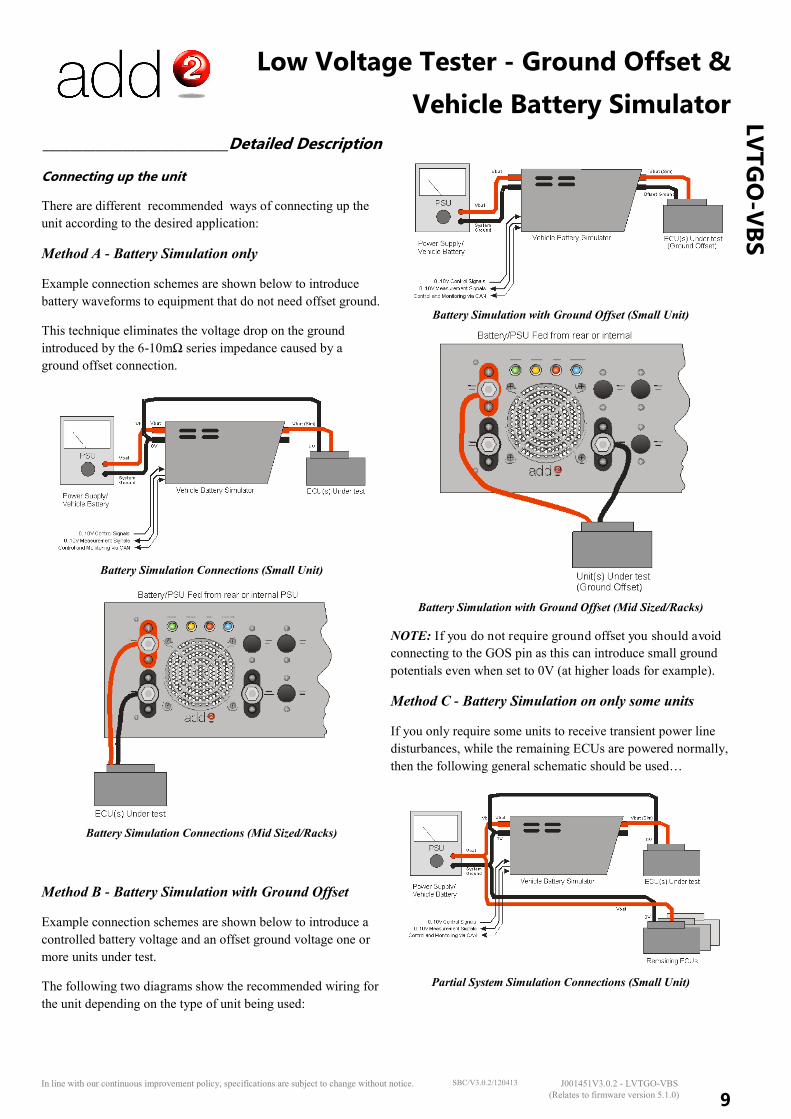
____________________________Detailed Description
Connecting up the unit
There are different recommended ways of connecting up the
unit according to the desired application:
Method A - Battery Simulation only
Example connection schemes are shown below to introduce
battery waveforms to equipment that do not need offset ground.
This technique eliminates the voltage drop on the ground
introduced by the 6-10mΩ series impedance caused by a
ground offset connection.
Battery Simulation Connections (Small Unit)
Battery Simulation Connections (Mid Sized/Racks)
Method B - Battery Simulation with Ground Offset
Example connection schemes are shown below to introduce a
controlled battery voltage and an offset ground voltage one or
more units under test.
The following two diagrams show the recommended wiring for
the unit depending on the type of unit being used:
Battery Simulation with Ground Offset (Small Unit)
Battery Simulation with Ground Offset (Mid Sized/Racks)
NOTE: If you do not require ground offset you should avoid
connecting to the GOS pin as this can introduce small ground
potentials even when set to 0V (at higher loads for example).
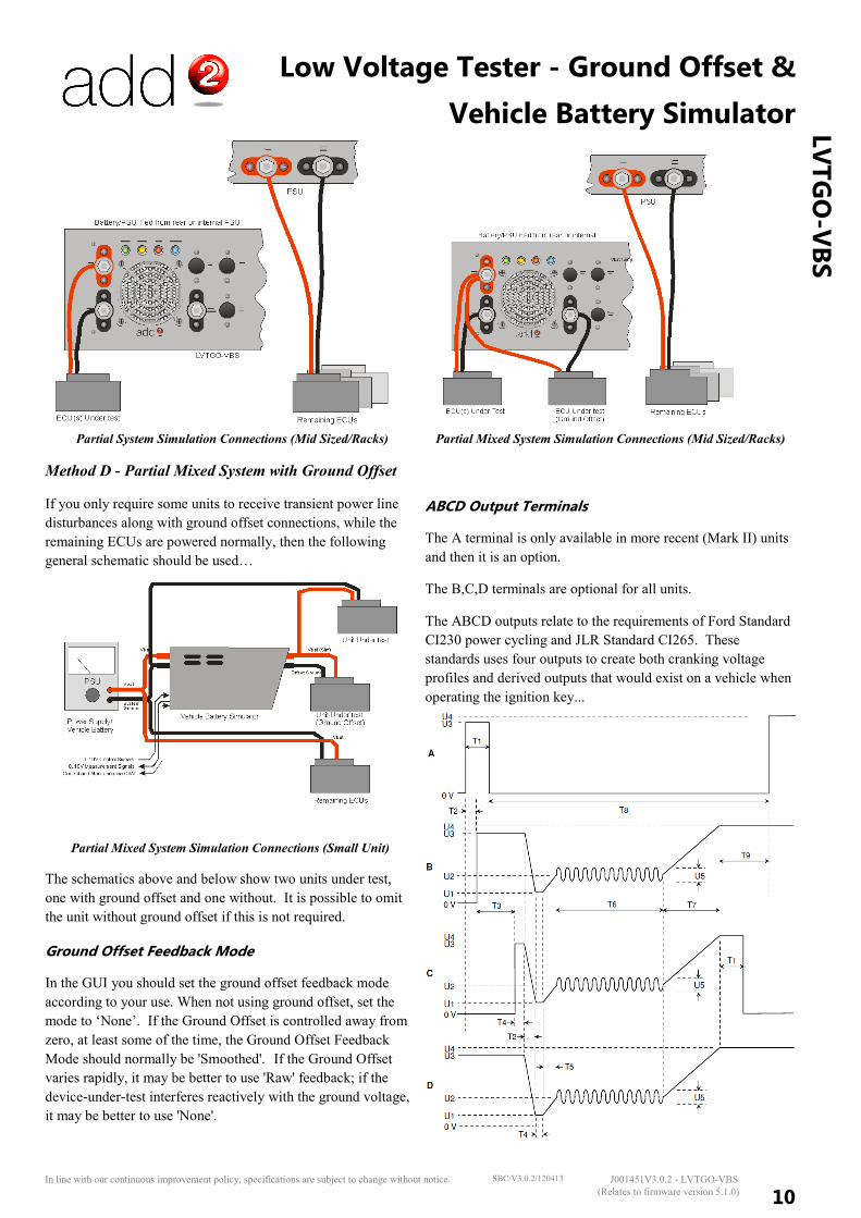
Method C - Battery Simulation on only some units
If you only require some units to receive transient power line
disturbances, while the remaining ECUs are powered normally,
then the following general schematic should be used…
Partial System Simulation Connections (Small Unit)
Low Voltage Tester - Ground Offset &
Vehicle Battery Simulator
10
LV
TG
O-V
BS
In line with our continuous improvement policy, specifications are subject to change without notice. J001451V3.0.2 - LVTGO-VBS SBC/V3.0.2/120413
(Relates to firmware version 5.1.0)
Partial System Simulation Connections (Mid Sized/Racks)
Method D - Partial Mixed System with Ground Offset
If you only require some units to receive transient power line
disturbances along with ground offset connections, while the
remaining ECUs are powered normally, then the following
general schematic should be used…
Partial Mixed System Simulation Connections (Small Unit)
The schematics above and below show two units under test,
one with ground offset and one without. It is possible to omit
the unit without ground offset if this is not required.
Ground Offset Feedback Mode
In the GUI you should set the ground offset feedback mode
according to your use. When not using ground offset, set the
mode to ‘None’. If the Ground Offset is controlled away from
zero, at least some of the time, the Ground Offset Feedback
Mode should normally be 'Smoothed'. If the Ground Offset
varies rapidly, it may be better to use 'Raw' feedback; if the
device-under-test interferes reactively with the ground voltage,
it may be better to use 'None'.
Partial Mixed System Simulation Connections (Mid Sized/Racks)
ABCD Output Terminals
The A terminal is only available in more recent (Mark II) units
and then it is an option.
The B,C,D terminals are optional for all units.
The ABCD outputs relate to the requirements of Ford Standard
CI230 power cycling and JLR Standard CI265. These
standards uses four outputs to create both cranking voltage
profiles and derived outputs that would exist on a vehicle when
operating the ignition key...
Low Voltage Tester - Ground Offset &
Vehicle Battery Simulator
11
LV
TG
O-V
BS
In line with our continuous improvement policy, specifications are subject to change without notice. J001451V3.0.2 - LVTGO-VBS SBC/V3.0.2/120413
(Relates to firmware version 5.1.0)
BCD Output
The BCD Outputs are supported on earlier LVTGO units - The
BCD outputs correspond to the BCD waveforms shown above.
The BCD outputs are driven from different resources within the
unit and exclude the use of the analogue output triggers when
in this mode.
The ABCD and BCD output options derive their signals from
the main output (Output D) and are switched at the appropriate
times to meet the specification as shown above.
To use the unit in this manner, a special profile must be opened
- This is to be found under the VISUALCONNX App folder...
<App>Profiles\Random Cranking WaveForm\CI265-2011.01.01\CI265
and the file to use is...
CI265.WaveformBCD.prw
The outputs [B] and [C] and sometimes [A] are physically
connected inside the unit and are presented on the front or rear
panel according to the images as follows...
B and C outputs - Small Unit
A, B and C outputs - Mid Sized and Rack Units
Note: Outputs A, B and C should be referenced to 0V if not
using the ground offset feature.
When running this (ABCD) profile the following typical
waveform way be seen at the four output pins…
This data was captured using a multi channel oscilloscope and data saved to excel.
Main Output Stage (Output D)
The LVTGO-VBS output stage can be configured under
software control. The output stage can be changed from High
Side Drive to Active High and Low drive. Active “High and
Low drive” allows the output to provide a fast transient
response on both rising and falling edges. On the GUI this is
marked as “Fast Output” on the U Settings Tab.
Fast Output allows the output to provide a fast connection
response and a slower disconnection response similar to that
of an intermittent connection on the battery;
The load impedance is then responsible for the waveform
characteristic.
Low Voltage Tester - Ground Offset &
Vehicle Battery Simulator
12
LV
TG
O-V
BS
In line with our continuous improvement policy, specifications are subject to change without notice. J001451V3.0.2 - LVTGO-VBS SBC/V3.0.2/120413
(Relates to firmware version 5.1.0)
Minimum load for Main Output
No minimum load is required on the Main Output terminal
provided you reference output D to the 0V terminal.
Note, however, if the system connected to the Output presents a
largely capacitive load, an additional load may be required if
not using the “Fast Output” setting on the U Settings tab for
full switching speeds to be achieved with fast transients.
Minimum load for Ground Offset
For optimum performance, when using ground offset it is
necessary to provide a minimum load between the main output
terminals Vout(D) and GNDOFFSET. (Marked VBOUT and
GNDOUT on the small unit)
50Ω minimum is recommended although lower resistance
values will improve accuracy at lower output voltages.
Most systems being tested will offer sufficient load if the
current consumption is 250mA or more without the need for a
50Ω load.
This requirement does not apply to the A, B and C output
terminals, unless you are not using output D.
NOTE: For the BCD outputs, there is a small leakage of
around 100uA per output which may affect the accuracy of
these lines - If very little load is presented to outputs B or C
you should also fit a minimum load of around 500Ohms. (This
does not apply to ABCD outputs on MK2 units).
Feeding supplies into the unit’s output terminals
If a battery or power supply is connected to the front
terminals (A,B,C or D) while “Fast Output” is turned on
this may cause permanent damage to the unit.
If this is likely to occur (eg: multi-battery systems) and fast
output is required, please contact add2 for further support and
solutions.
Low power supplies will not have the energy to damage the
unit, however this is still not recommended.
HIL I/O Connections
The rear of the LVTGO-VBS unit has a connector
designed for controlling the unit in “Analogue Control
Mode” or applying analogue trigger inputs to the unit.
Please refer to ‘Control Modes’ on page 7 for more
information on how to control the unit.
Please also refer to page 15 and 16 for more information.
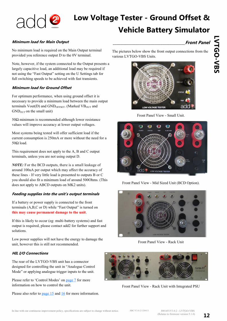
______________________________________Front Panel
The pictures below show the front output connections from the
various LVTGO-VBS Units.
Front Panel View - Small Unit.
Front Panel View - Mid Sized Unit (BCD Option).
Front Panel View - Rack Unit
Front Panel View - Rack Unit with Integrated PSU
Low Voltage Tester - Ground Offset &
Vehicle Battery Simulator
13
LV
TG
O-V
BS
In line with our continuous improvement policy, specifications are subject to change without notice. J001451V3.0.2 - LVTGO-VBS SBC/V3.0.2/120413
(Relates to firmware version 5.1.0)
Front Connections
Please refer to the front panel illustrations (above) for the unit
you are using. The 4mm/Screw terminals have the following
connections…
VOUTD - Main Battery Simulation Output
VOUTC1 - CI260/CI265 Multi Output C
VOUTB1 - CI260/CI265 Multi Output B
VOUTA1 - CI260/CI265 Multi Output A (MK2 Only)
VGND 0V (Near VOUTD) - 0V Reference Output
VPSU - PSU Output 2
VGND 0V (Near VPSU) - 0V Reference PSU 2
1 Optional Outputs, Mid-sized and Rack systems mainly.
2 Integrated PSU units only.
Where 4mm Sockets are fitted, the insulating tops for the
connectors unscrew to allow the use of ring terminals. A few
older units have tethered tops which do not unscrew fully.
Please use cable suitably rated for the currents being drawn, to
minimise voltage-drop between the unit and the device under
test.
WARNING: Do not short circuit any terminals
together and do not apply voltage to any front terminals
from any power sources including the internal PSU
terminals. Failure to observe these precautions may
damage the unit and will also void the warranty on the unit.
Front Panel Fuse
On units with integrated power supplies, the front panel fuse is
for the incoming mains supply. Replace with 10A quick blow
fuse if necessary after an overload condition.
Front Panel Switch
On units with integrated power supplies the front panel switch
is for the incoming mains supply. Press the switch down to
power up both the main PSU and the LVT electronics.
Front LEDs
Power LED
The Power LED is present on the front of the Mid-sized and
Rack based units. It is also present on the rear of the small unit.
The Power LED is green and indicates that the main control
board of theLVTGO-VBS is powered up.
Status LED
The Status LED is present on all units and indicates the
operational status of the unit.
The following table shows the status indication:
Trip LED
The Trip LED is red and lights up in a distinctive pattern to
indicate that a safety trip has occurred on the unit to protect the
hardware.
When the LED is lit, a buzzer sounds to draw attention to the
trip.
The following table show the LED patterns used:
There are three key reasons for a trip to occur:
a) Heat sink over-temperature
b) Battery and/or Ground driver stage over-power
c) Battery supply over-voltage
See also APPENDIX 4– TROUBLESHOOTING LVT ISSUES
Resetting Trips
When a trip has occurred, the unit will drive the Ground Offset
and Vbatt output voltages to zero. The Trip LED and the
buzzer will indicate that a trip has occurred.
After 30 seconds, if conditions allow, the trip will be reset. The
LED and buzzer will indicate that a trip has previously taken
place (see above table).
The unit will need to be power-cycled to return to normal
operation according to the type and severity of the trip.
Function LED
The function LED is only present on Mid-Sized and rack based
units.
The Function LED is a multi colour LED on units with the
microCUT board fitted, otherwise it is blue.
The purpose of the Function LED is to indicate the operational
mode of the unit’s Waveform Generator.
Low Voltage Tester - Ground Offset &
Vehicle Battery Simulator
14
LV
TG
O-V
BS
In line with our continuous improvement policy, specifications are subject to change without notice. J001451V3.0.2 - LVTGO-VBS SBC/V3.0.2/120413
(Relates to firmware version 5.1.0)
The following table describes the various function LED states
according to waveform generator output mode:
LVT FAN The LVT Fan is always towards the left hand-size of the unit.
Airflow
When the unit is powered, the LVT fan draws air from the side
panels of the enclosure and through the internal high-efficiency
heat-sink expelling the warm air from the front of the unit. The
unit must not be covered or restricted in air flow for full
performance to be achieved.
Fan speed
The LVT fan speed is controlled according to the internal
power and temperature of the unit.
Fan illumination
The LVT Fan housing is illuminated with blue light to indicate
that the power is on and to give some indication of internal
power dissipation. With zero internal power the unit will still
illuminate at a low level. With maximum power the unit will
illuminate brightly.
PSU FANS The PSU Fans are only available on units with integrated
power supplies.
Airflow
When the unit is powered, the PSU fans drawing air from the
front of the unit into the PSU. The unit must not be covered or
restricted in air flow for full performance to be achieved and to
protect the PSU from damage.
Fan speed
The PSU fan speed is controlled according to the internal
power and temperature of the PSU unit and additional output
loading.
Fan illumination
The PSU Fan housing is illuminated with blue light to indicate
that the power is on and to give some indication of fan speed.
Generally the brighter the PSU FAN LED the faster the fan is
turning, although please note that the PSU FAN LEDs are
usually brighter than the LVT FAN LEDs.
Safety Warnings
The fans may change speed at any time when power is applied.
Do not interfere with the fan mechanism or insert objects into
the fan grille.
The unit may become hot in use.
Do not cover the unit.
Under-rated cables may become dangerously hot, and may
introduce considerable voltage drops.
Ensure all LVT units, especially rack-mounted LVT units with
or without integrated power supplies have plenty of airflow
towards the rear of the unit.
Failure to observe these precautions may damage the unit
and will also void the warranty on the unit.
_______________________________________Rear Panel
The pictures below show the rear view of the LVTGO-VBS
units according to model…
Rear Panel View - Small Unit
Rear Panel View - Mid Sized Unit
Low Voltage Tester - Ground Offset &
Vehicle Battery Simulator
15
LV
TG
O-V
BS
In line with our continuous improvement policy, specifications are subject to change without notice. J001451V3.0.2 - LVTGO-VBS SBC/V3.0.2/120413
(Relates to firmware version 5.1.0)
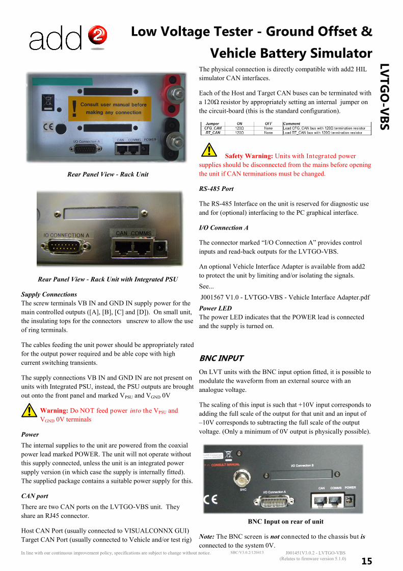
Rear Panel View - Rack Unit
Rear Panel View - Rack Unit with Integrated PSU
Supply Connections
The screw terminals VB IN and GND IN supply power for the
main controlled outputs ([A], [B], [C] and [D]). On small unit,
the insulating tops for the connectors unscrew to allow the use
of ring terminals.
The cables feeding the unit power should be appropriately rated
for the output power required and be able cope with high
current switching transients.
The supply connections VB IN and GND IN are not present on
units with Integrated PSU, instead, the PSU outputs are brought
out onto the front panel and marked VPSU and VGND 0V
Warning: Do NOT feed power into the VPSU and
VGND 0V terminals
Power
The internal supplies to the unit are powered from the coaxial
power lead marked POWER. The unit will not operate without
this supply connected, unless the unit is an integrated power
supply version (in which case the supply is internally fitted).
The supplied package contains a suitable power supply for this.
CAN port
There are two CAN ports on the LVTGO-VBS unit. They
share an RJ45 connector.
Host CAN Port (usually connected to VISUALCONNX GUI)
Target CAN Port (usually connected to Vehicle and/or test rig)
The physical connection is directly compatible with add2 HIL
simulator CAN interfaces.
Each of the Host and Target CAN buses can be terminated with
a 120Ω resistor by appropriately setting an internal jumper on
the circuit-board (this is the standard configuration).
Safety Warning: Units with Integrated power
supplies should be disconnected from the mains before opening
the unit if CAN terminations must be changed.
RS-485 Port
The RS-485 Interface on the unit is reserved for diagnostic use
and for (optional) interfacing to the PC graphical interface.
I/O Connection A
The connector marked “I/O Connection A” provides control
inputs and read-back outputs for the LVTGO-VBS.
An optional Vehicle Interface Adapter is available from add2
to protect the unit by limiting and/or isolating the signals.
See...
J001567 V1.0 - LVTGO-VBS - Vehicle Interface Adapter.pdf
Power LED
The power LED indicates that the POWER lead is connected
and the supply is turned on.
BNC INPUT
On LVT units with the BNC input option fitted, it is possible to
modulate the waveform from an external source with an
analogue voltage.
The scaling of this input is such that +10V input corresponds to
adding the full scale of the output for that unit and an input of
–10V corresponds to subtracting the full scale of the output
voltage. (Only a minimum of 0V output is physically possible).
BNC Input on rear of unit
Note: The BNC screen is not connected to the chassis but is
connected to the system 0V.
Low Voltage Tester - Ground Offset &
Vehicle Battery Simulator
16
LV
TG
O-V
BS
In line with our continuous improvement policy, specifications are subject to change without notice. J001451V3.0.2 - LVTGO-VBS SBC/V3.0.2/120413
(Relates to firmware version 5.1.0)
The full scale range of the BNC input relates to the nominal full scale of the unit, such as 20V or 30V. It is possible to exceed
nominal full scale by applying more than 10V input, depending on the supply voltage, up to the maximum trip voltage.
The BNC input is matched to 1MΩ @ 18pf and is protected for inputs up to +30V.
Thus, it is possible to apply a.c. inputs up to 100KHz (some roll off will occur above 10KHz depending on the option fitted) to
“modulate” the output via the BNC input from sources such as function generators, arbitrary waveform generators or the add2
CAN controlled H3 I/O Modules.
Note: The LVT requires the “Micro-Cut“ option fitted to support the BNC option.
Also note: To use the BNC modulation facility it is necessary to enable the function via the VISUALCONNX GUI.
BNC Connection Pinouts
Where the BNC input is fitted the pinouts are as follows...
Note: Do not per mit high power sources such as battery supplies to come into contact with the BNC Outer (0V) as
damage could occur to the unit.
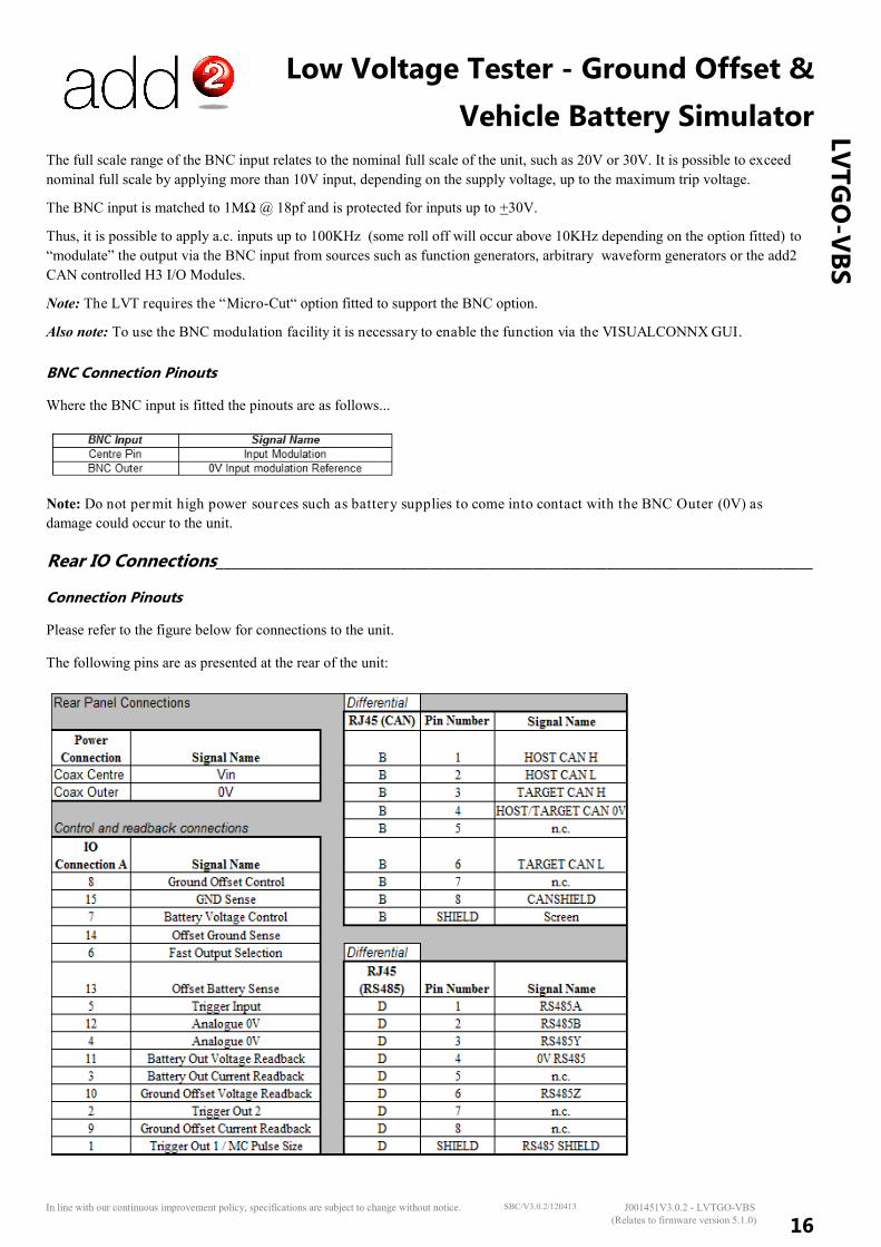
Rear IO Connections_________________________________________________________________________________
Connection Pinouts
Please refer to the figure below for connections to the unit.
The following pins are as presented at the rear of the unit:
Low Voltage Tester - Ground Offset &
Vehicle Battery Simulator
17
LV
TG
O-V
BS
In line with our continuous improvement policy, specifications are subject to change without notice. J001451V3.0.2 - LVTGO-VBS SBC/V3.0.2/120413
(Relates to firmware version 5.1.0)
__________________IO Connection A: Description
Inputs:
Ground Offset Control (analogue) 1
When using external analogue control mode the acceptable
input range is 0 to +10V; for example, a 1V control signal
applied (say from a HIL system) will produce a 0.25V constant
ground offset between the Rear 0V and the Front 0V.
Battery Voltage Control (analogue) 1
When using external analogue control mode the acceptable
input range is 0 to +10V; for example a 1V control signal
applied will produce a 10% full scale battery output between
the Front Battery and the Front GND connections (Depends on
the optional hardware range of 20V or 30V).
Fast Output Selection (analogue) 1
When fast output is on, the output stage utilises an ‘Active
High and Low’ configuration to ensure a fast falling output.
The output stage can be changed from ‘Active High and Low’
to ‘High Side Only’ Drive.
When not connected or with a voltage less than 2.5V, Active
High and Low drive is selected. When voltage is more than
2.5V, High Side Only Drive is selected.
Trigger Input (analogue) 1
The waveform signals, set up via the GUI, can be triggered
either via CAN messages or by using an analogue trigger. The
threshold between state logic 0 and logic 1 is 2.5V.
GND Sense
Not used.
Offset Ground Sense
When using remote sensing (cf. Remote voltage sensing p.8),
this wire needs to be connected to the ‘-’ of the load (ECU…).
Offset Battery Sense
When using remote sensing (cf. Remote voltage sensing p.8),
this wire needs to be connected to the ‘+’ of the load (ECU…).
Outputs:
Battery Out Voltage Readback
This signal produces a voltage proportional to the Offset
Voltage output. Its range varies from 0V to 10V for 0V to Full
Scale Battery output. (Depends on the optional hardware range
of 20V or 30V).
Battery Out Current Readback
This signal gives the current measurement of the ‘+’ side of the
load. It varies from 0V to 10V for 0A to 70A. (It is possible to
measure signals up to 122A through CAN messages (cf. Main
VCX Readback)
Ground Offset Voltage Readback
This signal produces a voltage proportional to the Ground
Offset output. Its range varies from 0V to 10V for a 0V to 2.5V
Ground Offset output.
Trigger Out 1
Trigger Out 1 is a digital 0..5V signal generated when using
output trigger set to Pin 1.
This output is reserved in microCUT output mode - In this
mode the output represents the pulse amplitude.
This output is also reserved in BCD output mode on MK1
hardware.
Do not short circuit this pin on MK1 boards
Trigger Out 2
Trigger Out 2 is a digital 0..5V signal generated when using
output trigger set to Pin 2.
This is the recommended pin to use for output triggering unless
two triggers are required.
This output is reserved in BCD output mode on MK1 hardware.
Do not short circuit this pin on MK1 boards
Ground Offset Current Readback
This signal gives the current measurement of the ‘-’ side of the
load. It varies from 0V to 10V for 0A to 70A. (It is possible to
measure signals up to 122A through CAN messages (cf. Main
VCX Readback).
General Information
Most of the readbacks (as well as the driven battery and ground
offset voltages) may additionally be read via the GUI in
software and via the COM interface.
These signals may also be logged via the GUI application.
Up to the last 1,000 sets of readbacks may be read using the
COM interface.
1 Do not exceed 12V d.c. on these control lines unless using
MK2 hardware or the vehicle interface adapter.
Voltages from 0V to –10V are tolerated but treated as 0V.
Low Voltage Tester - Ground Offset &
Vehicle Battery Simulator
18
LV
TG
O-V
BS
In line with our continuous improvement policy, specifications are subject to change without notice. J001451V3.0.2 - LVTGO-VBS SBC/V3.0.2/120413
(Relates to firmware version 5.1.0)
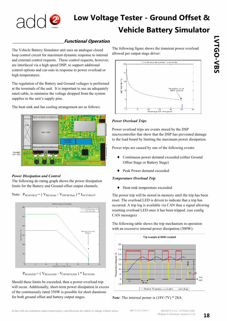
___________________________Functional Operation
The Vehicle Battery Simulator unit uses an analogue closed
loop control circuit for maximum dynamic response to internal
and external control requests. These control requests, however,
are interfaced via a high speed DSP, to support additional
control options and cut-outs in response to power overload or
high temperatures.
The regulation of the Battery and Ground voltages is performed
at the terminals of the unit. It is important to use an adequately
rated cable, to minimise the voltage dropped from the system
supplies to the unit’s supply pins.
The heat-sink and fan cooling arrangement are as follows:
Power Dissipation and Control
The following de-rating graph shows the power dissipation
limits for the Battery and Ground offset output channels.
Note: PMAXVBAT = ( VREALbatt - VOFFSETbatt ) * IOUTVBATT
PMAXGND = ( VREALGND - VOFFSETGND ) * IOUTGND
Should these limits be exceeded, then a power-overload trip
will occur. Additionally, short-term power dissipation in excess
of the continuously rated 350W is possible for short durations
for both ground offset and battery output stages.
The following figure shows the transient power overload
allowed per output stage driver:
Power Overload Trips
Power overload trips are events stored by the DSP
microcontroller that show that the DSP has prevented damage
to the load board by limiting the maximum power dissipation.
Power trips are caused by one of the following events:
Continuous power demand exceeded (either Ground
Offset Stage or Battery Stage)
Peak Power demand exceeded
Temperature Overload Trip
Heat-sink temperature exceeded
The power trip will be stored in memory until the trip has been
reset. The overload LED is driven to indicate that a trip has
occurred. A trip log is available via CAN thus a signal allowing
resetting overload LED once it has been tripped. (see config
CAN messages)
The following table shows the trip mechanism in operation
with an excessive internal power dissipation (300W):
Note: The internal power is (18V-7V) * 28A.
Low Voltage Tester - Ground Offset &
Vehicle Battery Simulator
19
LV
TG
O-V
BS
In line with our continuous improvement policy, specifications are subject to change without notice. J001451V3.0.2 - LVTGO-VBS SBC/V3.0.2/120413
(Relates to firmware version 5.1.0)
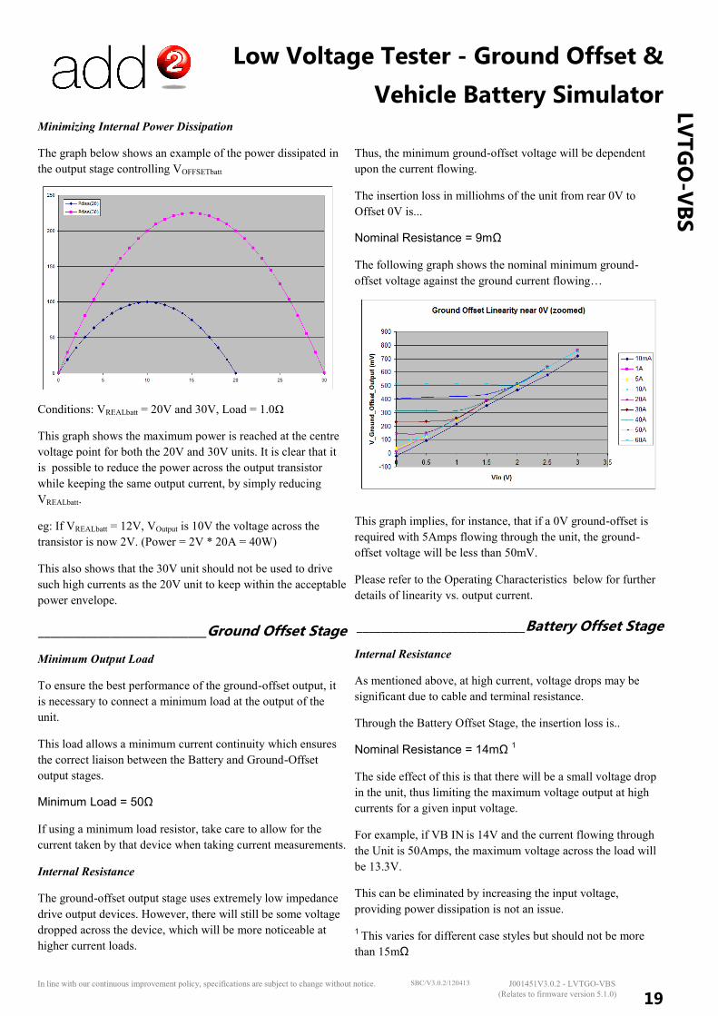
Minimizing Internal Power Dissipation
The graph below shows an example of the power dissipated in
the output stage controlling VOFFSETbatt
Conditions: VREALbatt = 20V and 30V, Load = 1.0Ω
This graph shows the maximum power is reached at the centre
voltage point for both the 20V and 30V units. It is clear that it
is possible to reduce the power across the output transistor
while keeping the same output current, by simply reducing
VREALbatt.
eg: If VREALbatt = 12V, VOutput is 10V the voltage across the
transistor is now 2V. (Power = 2V * 20A = 40W)
This also shows that the 30V unit should not be used to drive
such high currents as the 20V unit to keep within the acceptable
power envelope.
____________________________Ground Offset Stage
Minimum Output Load
To ensure the best performance of the ground-offset output, it
is necessary to connect a minimum load at the output of the
unit.
This load allows a minimum current continuity which ensures
the correct liaison between the Battery and Ground-Offset
output stages.
Minimum Load = 50Ω
If using a minimum load resistor, take care to allow for the
current taken by that device when taking current measurements.
Internal Resistance
The ground-offset output stage uses extremely low impedance
drive output devices. However, there will still be some voltage
dropped across the device, which will be more noticeable at
higher current loads.
Thus, the minimum ground-offset voltage will be dependent
upon the current flowing.
The insertion loss in milliohms of the unit from rear 0V to
Offset 0V is...
Nominal Resistance = 9mΩ
The following graph shows the nominal minimum ground-
offset voltage against the ground current flowing…
This graph implies, for instance, that if a 0V ground-offset is
required with 5Amps flowing through the unit, the ground-
offset voltage will be less than 50mV.
Please refer to the Operating Characteristics below for further
details of linearity vs. output current.
____________________________Battery Offset Stage
Internal Resistance
As mentioned above, at high current, voltage drops may be
significant due to cable and terminal resistance.
Through the Battery Offset Stage, the insertion loss is..
Nominal Resistance = 14mΩ 1
The side effect of this is that there will be a small voltage drop
in the unit, thus limiting the maximum voltage output at high
currents for a given input voltage.
For example, if VB IN is 14V and the current flowing through
the Unit is 50Amps, the maximum voltage across the load will
be 13.3V.
This can be eliminated by increasing the input voltage,
providing power dissipation is not an issue.
1 This varies for different case styles but should not be more
than 15mΩ
Low Voltage Tester - Ground Offset &
Vehicle Battery Simulator
20
LV
TG
O-V
BS
In line with our continuous improvement policy, specifications are subject to change without notice. J001451V3.0.2 - LVTGO-VBS SBC/V3.0.2/120413
(Relates to firmware version 5.1.0)
Over-voltage Protection
If the battery voltage exceeds 22.5V on the 20V unit, or 33V on
the 30V unit then the output will go into a tripped state until it
falls below the acceptable limits (22.0V and 32.6V) .
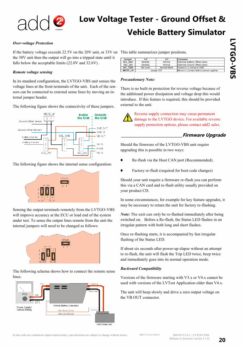
Remote voltage sensing
In its standard configuration, the LVTGO-VBS unit senses the
voltage lines at the front terminals of the unit. Each of the sen-
sors can be connected to external sense lines by moving an in-
ternal jumper header.
The following figure shows the connectivity of these jumpers.
The following figure shows the internal sense configuration:
Sensing the output terminals remotely from the LVTGO-VBS
will improve accuracy at the ECU or load end of the system
under test. To sense the output lines remote from the unit the
internal jumpers will need to be changed as follows:
The following schema shows how to connect the remote sense
lines.
This table summarizes jumper positions.
Precautionary Note:
There is no built-in protection for reverse voltage because of
the additional power dissipation and voltage drop this would
introduce. If this feature is required, this should be provided
external to the unit.
Reverse supply connection may cause permanent
damage to the LVTGO device. For available reverse
supply protection options, please contact add2 sales.
______________________________Firmware Upgrade
Should the firmware of the LVTGO-VBS unit require
upgrading this is possible in two ways:
Re-flash via the Host CAN port (Recommended).
Factory re-flash (required for boot code changes)
Should your unit require a firmware re-flash you can perform
this via a CAN card and re-flash utility usually provided on
your product CD.
In some circumstances, for example for key feature upgrades, it
may be necessary to return the unit for factory re-flashing.
Note: The unit can only be re-flashed immediately after being
switched on. Before a Re-flash, the Status LED flashes in an
irregular pattern with both long and short flashes.
Once re-flashing starts, it is accompanied by fast irregular
flashing of the Status LED.
If about six seconds after power-up elapse without an attempt
to re-flash, the unit will flash the Trip LED twice, beep twice
and immediately goes into its normal operation mode.
Backward Compatibility
Versions of the firmware starting with V3.x or V4.x cannot be
used with versions of the LVTest Application older than V4.x.
The unit will beep slowly and drive a zero output voltage on
the VB OUT connector.
Low Voltage Tester - Ground Offset &
Vehicle Battery Simulator
21
LV
TG
O-V
BS
In line with our continuous improvement policy, specifications are subject to change without notice. J001451V3.0.2 - LVTGO-VBS SBC/V3.0.2/120413
(Relates to firmware version 5.1.0)
LVTGO-VBS CAN MESSAGING
Introduction
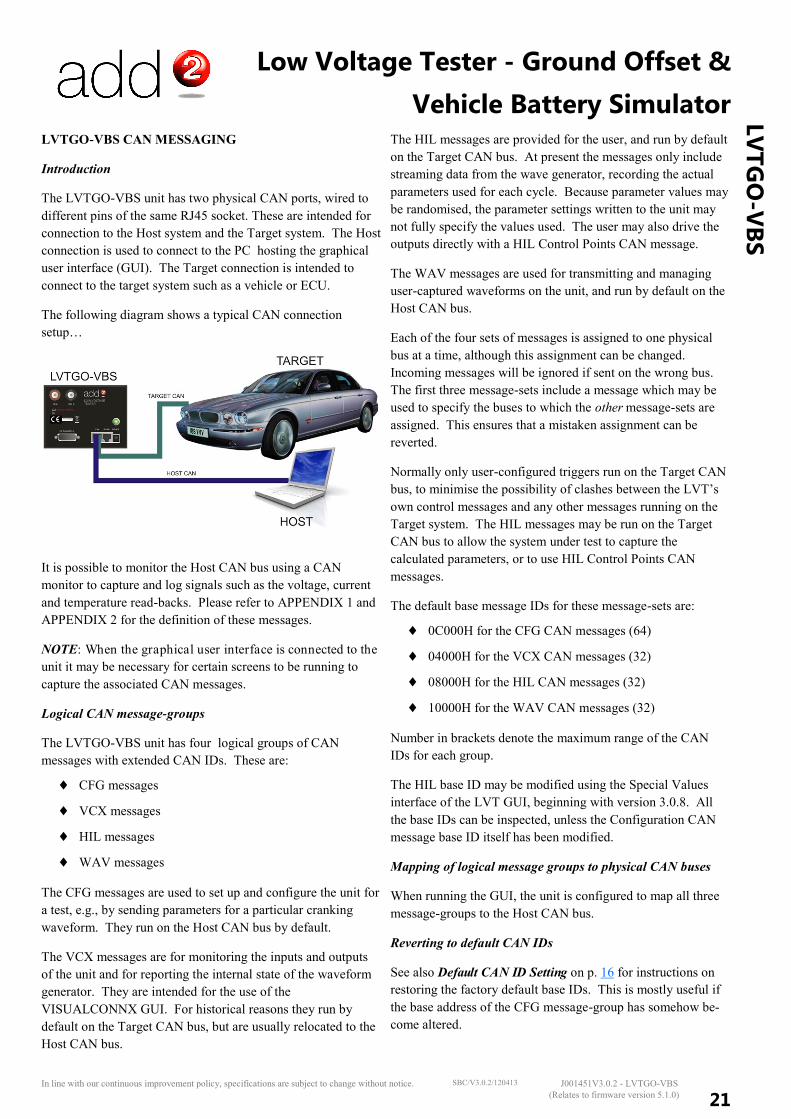
The LVTGO-VBS unit has two physical CAN ports, wired to
different pins of the same RJ45 socket. These are intended for
connection to the Host system and the Target system. The Host
connection is used to connect to the PC hosting the graphical
user interface (GUI). The Target connection is intended to
connect to the target system such as a vehicle or ECU.
The following diagram shows a typical CAN connection
setup…
It is possible to monitor the Host CAN bus using a CAN
monitor to capture and log signals such as the voltage, current
and temperature read-backs. Please refer to APPENDIX 1 and
APPENDIX 2 for the definition of these messages.
NOTE: When the graphical user interface is connected to the
unit it may be necessary for certain screens to be running to
capture the associated CAN messages.
Logical CAN message-groups
The LVTGO-VBS unit has four logical groups of CAN
messages with extended CAN IDs. These are:
CFG messages
VCX messages
HIL messages
WAV messages
The CFG messages are used to set up and configure the unit for
a test, e.g., by sending parameters for a particular cranking
waveform. They run on the Host CAN bus by default.
The VCX messages are for monitoring the inputs and outputs
of the unit and for reporting the internal state of the waveform
generator. They are intended for the use of the
VISUALCONNX GUI. For historical reasons they run by
default on the Target CAN bus, but are usually relocated to the
Host CAN bus.
The HIL messages are provided for the user, and run by default
on the Target CAN bus. At present the messages only include
streaming data from the wave generator, recording the actual
parameters used for each cycle. Because parameter values may
be randomised, the parameter settings written to the unit may
not fully specify the values used. The user may also drive the
outputs directly with a HIL Control Points CAN message.
The WAV messages are used for transmitting and managing
user-captured waveforms on the unit, and run by default on the
Host CAN bus.
Each of the four sets of messages is assigned to one physical
bus at a time, although this assignment can be changed.
Incoming messages will be ignored if sent on the wrong bus.
The first three message-sets include a message which may be
used to specify the buses to which the other message-sets are
assigned. This ensures that a mistaken assignment can be
reverted.
Normally only user-configured triggers run on the Target CAN
bus, to minimise the possibility of clashes between the LVT’s
own control messages and any other messages running on the
Target system. The HIL messages may be run on the Target
CAN bus to allow the system under test to capture the
calculated parameters, or to use HIL Control Points CAN
messages.
The default base message IDs for these message-sets are:
0C000H for the CFG CAN messages (64)
04000H for the VCX CAN messages (32)
08000H for the HIL CAN messages (32)
10000H for the WAV CAN messages (32)
Number in brackets denote the maximum range of the CAN
IDs for each group.
The HIL base ID may be modified using the Special Values
interface of the LVT GUI, beginning with version 3.0.8. All
the base IDs can be inspected, unless the Configuration CAN
message base ID itself has been modified.
Mapping of logical message groups to physical CAN buses
When running the GUI, the unit is configured to map all three
message-groups to the Host CAN bus.
Reverting to default CAN IDs
See also Default CAN ID Setting on p. 16 for instructions on
restoring the factory default base IDs. This is mostly useful if
the base address of the CFG message-group has somehow be-
come altered.
Low Voltage Tester - Ground Offset &
Vehicle Battery Simulator
22
LV
TG
O-V
BS
In line with our continuous improvement policy, specifications are subject to change without notice. J001451V3.0.2 - LVTGO-VBS SBC/V3.0.2/120413
(Relates to firmware version 5.1.0)
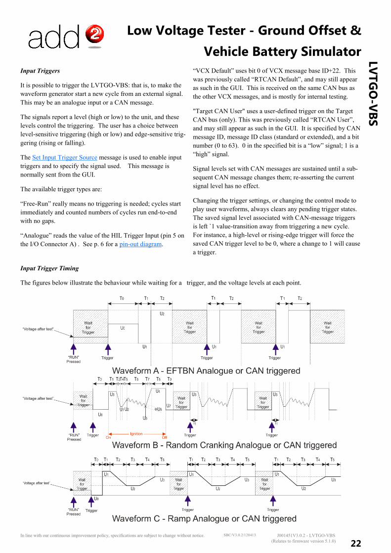
Input Triggers
It is possible to trigger the LVTGO-VBS: that is, to make the
waveform generator start a new cycle from an external signal.
This may be an analogue input or a CAN message.
The signals report a level (high or low) to the unit, and these
levels control the triggering. The user has a choice between
level-sensitive triggering (high or low) and edge-sensitive trig-
gering (rising or falling).
The Set Input Trigger Source message is used to enable input
triggers and to specify the signal used. This message is
normally sent from the GUI.
The available trigger types are:
“Free-Run” really means no triggering is needed; cycles start
immediately and counted numbers of cycles run end-to-end
with no gaps.
“Analogue” reads the value of the HIL Trigger Input (pin 5 on
the I/O Connector A) . See p. 6 for a pin-out diagram.
“VCX Default” uses bit 0 of VCX message base ID+22. This
was previously called “RTCAN Default”, and may still appear
as such in the GUI. This is received on the same CAN bus as
the other VCX messages, and is mostly for internal testing.
"Target CAN User" uses a user-defined trigger on the Target
CAN bus (only). This was previously called “RTCAN User”,
and may still appear as such in the GUI. It is specified by CAN
message ID, message ID class (standard or extended), and a bit
number (0 to 63). 0 in the specified bit is a “low” signal; 1 is a
“high” signal.
Signal levels set with CAN messages are sustained until a sub-
sequent CAN message changes them; re-asserting the current
signal level has no effect.
Changing the trigger settings, or changing the control mode to
play user waveforms, always clears any pending trigger states.
The saved signal level associated with CAN-message triggers
is left `1 value-transition away from triggering a new cycle.
For instance, a high-level or rising-edge trigger will force the
saved CAN trigger level to be 0, where a change to 1 will cause
a trigger.
Input Trigger Timing
The figures below illustrate the behaviour while waiting for a trigger, and the voltage levels at each point.
Low Voltage Tester - Ground Offset &
Vehicle Battery Simulator
23
LV
TG
O-V
BS
In line with our continuous improvement policy, specifications are subject to change without notice. J001451V3.0.2 - LVTGO-VBS SBC/V3.0.2/120413
(Relates to firmware version 5.1.0)
Output Triggers
The LVTGO-VBS can be used to generate triggers for the
user’s own hardware. These may be analogue signals or CAN
messages. A trigger is emitted at a configurable time (1 to
65535 ms) after the start of a nominated waveform stage
(corresponding to the T parameters for that waveform), unless
the waveform cycle ends first.
The Configure Output Trigger message is used to enable
triggers and to specify the signal used. This message is
normally sent from the GUI. Versions of the GUI starting with
3.0.8 also support additional features of the firmware. A “Type
1” message may be sent to set the pulse width (only), A variant
“Type 2” message is like the default “Type 0” message, but the
time-interval specified is measured from the end of the
specified step, not from the beginning. This is subject to an
important restriction. The trigger cannot be emitted until the
length of the specified step is known, which will only occur
after it begins. A trigger will be emitted if, when the length of
the step is known, it is found that it should already have been
emitted. This mechanism cannot be used to cause a trigger to
be emitted during an earlier step.
The available trigger types are:
“Analogue pin 1” replaces the usual Temperature analogue
output (pin 1 on the I/O Connector A) with a trigger signal.
This pin is not available in microCUT mode.
“Analogue pin 2” replaces the usual Trip analogue output (pin
2 on the I/O Connector A) with a trigger signal.
“Target CAN” sends a user-configured trigger frame.
An analogue trigger is a 5V positive-going pulse with a
nominated width (1 to 65535 ms: 0 is not allowed). The pulse
will be cut off at the end of the cycle if it has not already timed
out.
A CAN trigger can only be sent on the Target CAN bus. It is
specified by CAN message ID, message ID class (standard or
extended), and data length (0-8 for 0-8 bytes). If this is
configured and the data length is not 0, then the contents of the
message to be sent must be supplied in a “Set Output Trigger
Contents” message, Configuration message base ID + 24.
Conflicts with Trigger IDs
User-configured trigger CAN IDs, both for input and output
triggers, may potentially clash with CAN IDs reserved for the
use of the LVTester GUI interface. A standard ID will never
conflict, because all of the pre-defined messages for the LVT
use extended IDs.
Each message-group reserves the extended IDs from its Base
ID to its Base ID + 31 inclusive, but only on the bus to which it
is assigned. User-configured input triggers are not allowed to
fall in a reserved range. An attempt to configure a user input
trigger which creates a conflict will fail. Changing the assigned
bus of a message-group, or changing its base ID, may also
create a conflict. In that case the bus is reconfigured as
intended, but the trigger source is set to “None (free-run)”.
In all these cases, an error message is sent from the LVT. This
behaviour does not depend on the control mode of the unit.
For instance, the waveform generator need not be in use at all.
Output Trigger Timing
The diagrams on the following page illustrate the effect of the timing settings on analogue
triggers. A CAN trigger, if configured, would be sent at the same time that the analogue
trigger pulse begins.
Waveform A shows that an analogue pulse will not be cut short by the end of the current
waveform stage, unless this is also the end of the current cycle (as in Waveform C).
Waveform B shows that the waveform stage which starts the timer for the trigger need not
still be current when the trigger is sent.
A trigger on stage T0 will only be sent on the very first cycle of a run, because later runs
begin with T1 and not T0.
Low Voltage Tester - Ground Offset &
Vehicle Battery Simulator
24
LV
TG
O-V
BS
In line with our continuous improvement policy, specifications are subject to change without notice. J001451V3.0.2 - LVTGO-VBS SBC/V3.0.2/120413
(Relates to firmware version 5.1.0)
Low Voltage Tester - Ground Offset &
Vehicle Battery Simulator
25
LV
TG
O-V
BS
In line with our continuous improvement policy, specifications are subject to change without notice. J001451V3.0.2 - LVTGO-VBS SBC/V3.0.2/120413
(Relates to firmware version 5.1.0)
Alternative Output Triggers
Starting with version 1.4.0 of the firmware, there is another and
more flexible way to configure the output triggers. Each of the
existing analogue outputs (pin 1 and pin 2) may be driven1,
with separate configuration of the rising and falling edges. The
options available still allow triggers to be timed before the end
of a step rather than from the beginning of a step, but this will
not actually cause an edge to be emitted before the beginning of
the specified step. At earliest, it will occur when the length of
the step is known, which is normally 1 ms after the voltage for
the beginning of the step is driven.
The falling edge may occur earlier than the rising edge. After
configuration, the firmware attempts to get the initial level
correct. It ignores the current step and sets the initial step as
though for the beginning of a cycle. It is assumed that if the
falling edge is anchored to a step earlier than the rising edge,
the initial level should be high. A long positive delay on an
earlier step may time out after the later step, and the initial level
may then turn out to be wrong. Similarly, if the edges are an-
chored to the same step, it is assumed that the specified delays
(if measured in the same direction, both from the beginning of
the step or both from the end of the step) determine the order of
the edges. This may be false if long delays from the end of the
step are both actually converted into the same moment, when
the length of the step is known. If the edges are anchored to the
beginning and to the end of the same step, then the initial
voltage level is always low.
1 Only pin 2 may be used as an analogue output trigger for
microCUT modes. During this mode the pin outputs a value
representative of the amplitude.
CONFIGURATION FOR SPECIAL OPERATING
MODES
DIP Switch Settings
There is a block of eight DIP switches on the main board of the
unit, numbered 1 to 8. These should normally all be “off” - that
is, looking at the DIP switches from the nearest edge of the
board, on the same side of the board as the switches
themselves, they should be thrown to the left. Normal
operation is only guaranteed in this configuration.
The switches should only be moved when the power is off as
the state of the switches will only be sampled when the unit is
powered on.
Currently two alternative settings are defined as meaningful.
Calibration Setting
If the odd-numbered switches are “on” and the even-numbered
switches are “off”, the unit is in a special calibration mode.
This requires additional hardware and software support and is
not intended for customer use. If a unit is believed to require
fresh calibration, it should be returned to add2.
Default CAN ID Setting
The CAN messages used by the LVT are divided into separate
message-groups, each of which has a separately configured
base CAN ID. See p. 11 for more details.
If for any reason some message-group other than the HIL
message-group becomes relocated to a base ID which is not the
factory default, the LVT Application interface will not work..
In the worst case, the CFG message-set may be relocated, and
then there is no way even to determine the current values of the
base IDs.
If switches 1, 2, 7 and 8 are “on” and the others are “off”, the
unit operates almost exactly as normal, but when starting the
unit the currently configured CAN base IDs are ignored and
overwritten with the default values. This takes place just after
the Trip LED flashes twice and the buzzer sounds. Wait an
additional second or so before switching off again to allow the
restored default values to be saved.
Low Voltage Tester - Ground Offset &
Vehicle Battery Simulator
26
LV
TG
O-V
BS
In line with our continuous improvement policy, specifications are subject to change without notice. J001451V3.0.2 - LVTGO-VBS SBC/V3.0.2/120413
(Relates to firmware version 5.1.0)
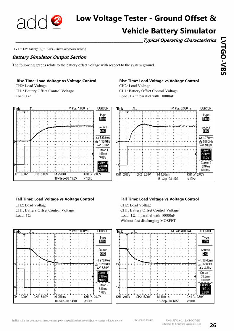
_________________________________________________________________Typical Operating Characteristics
(V+ = 12V battery, TA = +26oC, unless otherwise noted.)
Battery Simulator Output Section
The following graphs relate to the battery offset voltage with respect to the system ground.
Rise Time: Load Voltage vs Voltage Control
CH2: Load Voltage
CH1: Battery Offset Control Voltage
Load: 1Ω
Fall Time: Load Voltage vs Voltage Control
CH2: Load Voltage
CH1: Battery Offset Control Voltage
Load: 1Ω
CH2: Load Voltage
CH1: Battery Offset Control Voltage
Load: 1Ω in parallel with 10000uF
Without fast discharging MOSFET
Rise Time: Load Voltage vs Voltage Control
CH2: Load Voltage
CH1: Battery Offset Control Voltage
Load: 1Ω in parallel with 10000uF
Fall Time: Load Voltage vs Voltage Control
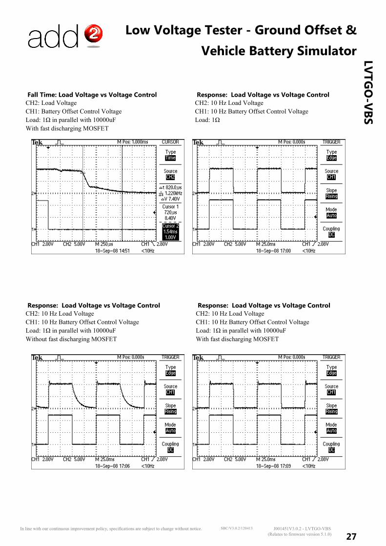
Low Voltage Tester - Ground Offset &
Vehicle Battery Simulator
27
LV
TG
O-V
BS
In line with our continuous improvement policy, specifications are subject to change without notice. J001451V3.0.2 - LVTGO-VBS SBC/V3.0.2/120413
(Relates to firmware version 5.1.0)
Fall Time: Load Voltage vs Voltage Control
CH2: Load Voltage
CH1: Battery Offset Control Voltage
Load: 1Ω in parallel with 10000uF
With fast discharging MOSFET
Response: Load Voltage vs Voltage Control
CH2: 10 Hz Load Voltage
CH1: 10 Hz Battery Offset Control Voltage
Load: 1Ω
Response: Load Voltage vs Voltage Control
CH2: 10 Hz Load Voltage
CH1: 10 Hz Battery Offset Control Voltage
Load: 1Ω in parallel with 10000uF
Without fast discharging MOSFET
Response: Load Voltage vs Voltage Control
CH2: 10 Hz Load Voltage
CH1: 10 Hz Battery Offset Control Voltage
Load: 1Ω in parallel with 10000uF
With fast discharging MOSFET
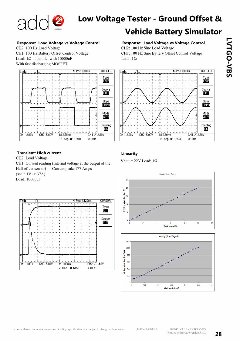
Low Voltage Tester - Ground Offset &
Vehicle Battery Simulator
28
LV
TG
O-V
BS
In line with our continuous improvement policy, specifications are subject to change without notice. J001451V3.0.2 - LVTGO-VBS SBC/V3.0.2/120413
(Relates to firmware version 5.1.0)
Response: Load Voltage vs Voltage Control
CH2: 100 Hz Load Voltage
CH1: 100 Hz Battery Offset Control Voltage
Load: 1Ω in parallel with 10000uF
With fast discharging MOSFET
Response: Load Voltage vs Voltage Control
CH2: 100 Hz Sine Load Voltage
CH1: 100 Hz Sine Battery Offset Control Voltage
Load: 1Ω
Transient: High current
CH2: Load Voltage
CH1: Current reading (Internal voltage at the output of the
Hall-effect sensor) — Current peak: 177 Amps
(scale 1V -> 37A)
Load: 10000uF
Linearity
Vbatt = 22V Load: 1Ω
Low Voltage Tester - Ground Offset &
Vehicle Battery Simulator
29
LV
TG
O-V
BS
In line with our continuous improvement policy, specifications are subject to change without notice. J001451V3.0.2 - LVTGO-VBS SBC/V3.0.2/120413
(Relates to firmware version 5.1.0)
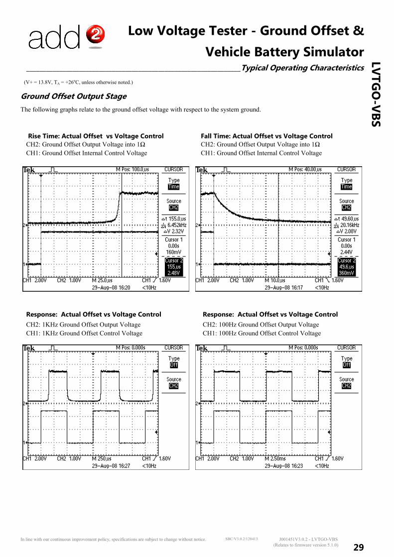
_________________________________________________________________Typical Operating Characteristics
(V+ = 13.8V, TA = +26oC, unless otherwise noted.)
Ground Offset Output Stage
The following graphs relate to the ground offset voltage with respect to the system ground.
Rise Time: Actual Offset vs Voltage Control
CH2: Ground Offset Output Voltage into 1Ω
CH1: Ground Offset Internal Control Voltage
Response: Actual Offset vs Voltage Control
CH2: 1KHz Ground Offset Output Voltage
CH1: 1KHz Ground Offset Control Voltage CH2: 100Hz Ground Offset Output Voltage
CH1: 100Hz Ground Offset Control Voltage
Fall Time: Actual Offset vs Voltage Control
CH2: Ground Offset Output Voltage into 1Ω
CH1: Ground Offset Internal Control Voltage
Response: Actual Offset vs Voltage Control
Low Voltage Tester - Ground Offset &
Vehicle Battery Simulator
30
LV
TG
O-V
BS
In line with our continuous improvement policy, specifications are subject to change without notice. J001451V3.0.2 - LVTGO-VBS SBC/V3.0.2/120413
(Relates to firmware version 5.1.0)
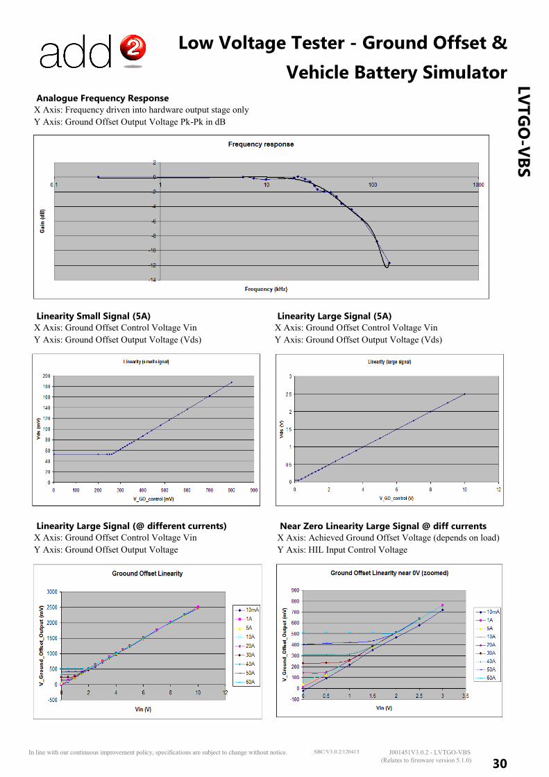
Linearity Small Signal (5A)
X Axis: Ground Offset Control Voltage Vin
Y Axis: Ground Offset Output Voltage (Vds)
Linearity Large Signal (5A)
X Axis: Ground Offset Control Voltage Vin Y Axis: Ground Offset Output Voltage (Vds)
Analogue Frequency Response
X Axis: Frequency driven into hardware output stage only Y Axis: Ground Offset Output Voltage Pk-Pk in dB
Linearity Large Signal (@ different currents)
X Axis: Ground Offset Control Voltage Vin Y Axis: Ground Offset Output Voltage
X Axis: Achieved Ground Offset Voltage (depends on load) Y Axis: HIL Input Control Voltage
Near Zero Linearity Large Signal @ diff currents
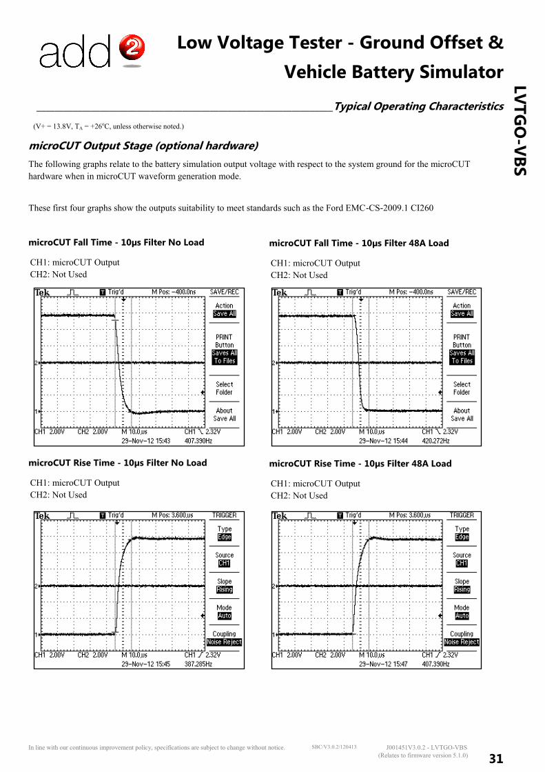
Low Voltage Tester - Ground Offset &
Vehicle Battery Simulator
31
LV
TG
O-V
BS
In line with our continuous improvement policy, specifications are subject to change without notice. J001451V3.0.2 - LVTGO-VBS SBC/V3.0.2/120413
(Relates to firmware version 5.1.0)
microCUT Fall Time - 10µs Filter No Load
CH1: microCUT Output
CH2: Not Used
_________________________________________________________________Typical Operating Characteristics
(V+ = 13.8V, TA = +26oC, unless otherwise noted.)
microCUT Output Stage (optional hardware)
The following graphs relate to the battery simulation output voltage with respect to the system ground for the microCUT
hardware when in microCUT waveform generation mode.
microCUT Fall Time - 10µs Filter 48A Load
CH1: microCUT Output
CH2: Not Used
microCUT Rise Time - 10µs Filter No Load
CH1: microCUT Output
CH2: Not Used
microCUT Rise Time - 10µs Filter 48A Load
CH1: microCUT Output
CH2: Not Used
These first four graphs show the outputs suitability to meet standards such as the Ford EMC-CS-2009.1 CI260
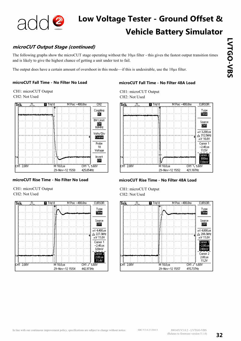
Low Voltage Tester - Ground Offset &
Vehicle Battery Simulator
32
LV
TG
O-V
BS
In line with our continuous improvement policy, specifications are subject to change without notice. J001451V3.0.2 - LVTGO-VBS SBC/V3.0.2/120413
(Relates to firmware version 5.1.0)
microCUT Fall Time - No Filter No Load
CH1: microCUT Output
CH2: Not Used
microCUT Output Stage (continued)
The following graphs show the microCUT stage operating without the 10µs filter - this gives the fastest output transition times
and is likely to give the highest chance of getting a unit under test to fail.
The output does have a certain amount of overshoot in this mode—if this is undesirable, use the 10µs filter.
microCUT Fall Time - No Filter 48A Load
CH1: microCUT Output
CH2: Not Used
microCUT Rise Time - No Filter No Load
CH1: microCUT Output
CH2: Not Used
microCUT Rise Time - No Filter 48A Load
CH1: microCUT Output
CH2: Not Used
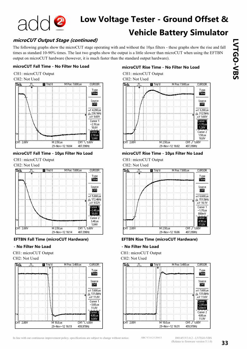
Low Voltage Tester - Ground Offset &
Vehicle Battery Simulator
33
LV
TG
O-V
BS
In line with our continuous improvement policy, specifications are subject to change without notice. J001451V3.0.2 - LVTGO-VBS SBC/V3.0.2/120413
(Relates to firmware version 5.1.0)
microCUT Fall Time - No Filter No Load
CH1: microCUT Output
CH2: Not Used
microCUT Output Stage (continued)
The following graphs show the microCUT stage operating with and without the 10µs filters - these graphs show the rise and fall
times as standard 10-90% times. The last two graphs show the output is a little slower than microCUT when using the EFTBN
output on microCUT hardware (however, it is much faster than the standard output hardware).
microCUT Rise Time - No Filter No Load
CH1: microCUT Output
CH2: Not Used
microCUT Fall Time - 10µs Filter No Load
CH1: microCUT Output
CH2: Not Used
microCUT Rise Time - 10µs Filter No Load
CH1: microCUT Output
CH2: Not Used
EFTBN Fall Time (microCUT Hardware)
- No Filter No Load
CH1: microCUT Output
CH2: Not Used
EFTBN Rise Time (microCUT Hardware)
- No Filter No Load
CH1: microCUT Output
CH2: Not Used
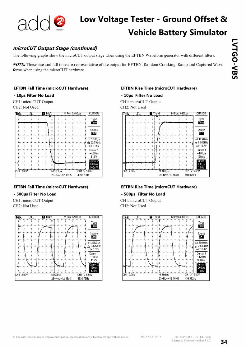
Low Voltage Tester - Ground Offset &
Vehicle Battery Simulator
34
LV
TG
O-V
BS
In line with our continuous improvement policy, specifications are subject to change without notice. J001451V3.0.2 - LVTGO-VBS SBC/V3.0.2/120413
(Relates to firmware version 5.1.0)
microCUT Output Stage (continued)
The following graphs show the microCUT output stage when using the EFTBN Waveform generator with different filters.
NOTE: These rise and fall time are representative of the output for EFTBN, Random Cranking, Ramp and Captured Wave-
forms when using the microCUT hardware
EFTBN Fall Time (microCUT Hardware)
- 10µs Filter No Load
CH1: microCUT Output
CH2: Not Used
EFTBN Rise Time (microCUT Hardware)
- 10µs Filter No Load
CH1: microCUT Output
CH2: Not Used
EFTBN Fall Time (microCUT Hardware)
- 500µs Filter No Load
CH1: microCUT Output
CH2: Not Used
EFTBN Rise Time (microCUT Hardware)
- 500µs Filter No Load
CH1: microCUT Output
CH2: Not Used
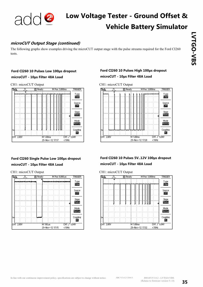
Low Voltage Tester - Ground Offset &
Vehicle Battery Simulator
35
LV
TG
O-V
BS
In line with our continuous improvement policy, specifications are subject to change without notice. J001451V3.0.2 - LVTGO-VBS SBC/V3.0.2/120413
(Relates to firmware version 5.1.0)
microCUT Output Stage (continued)
The following graphs show examples driving the microCUT output stage with the pulse streams required for the Ford CI260
tests.
Ford CI260 10 Pulses Low 100µs dropout
microCUT - 10µs Filter 48A Load
CH1: microCUT Output CH1: microCUT Output
Ford CI260 10 Pulses High 100µs dropout
microCUT - 10µs Filter 48A Load
Ford CI260 Single Pulse Low 100µs dropout
microCUT - 10µs Filter 48A Load
CH1: microCUT Output CH1: microCUT Output
Ford CI260 10 Pulses 5V..12V 100µs dropout
microCUT - 10µs Filter 48A Load
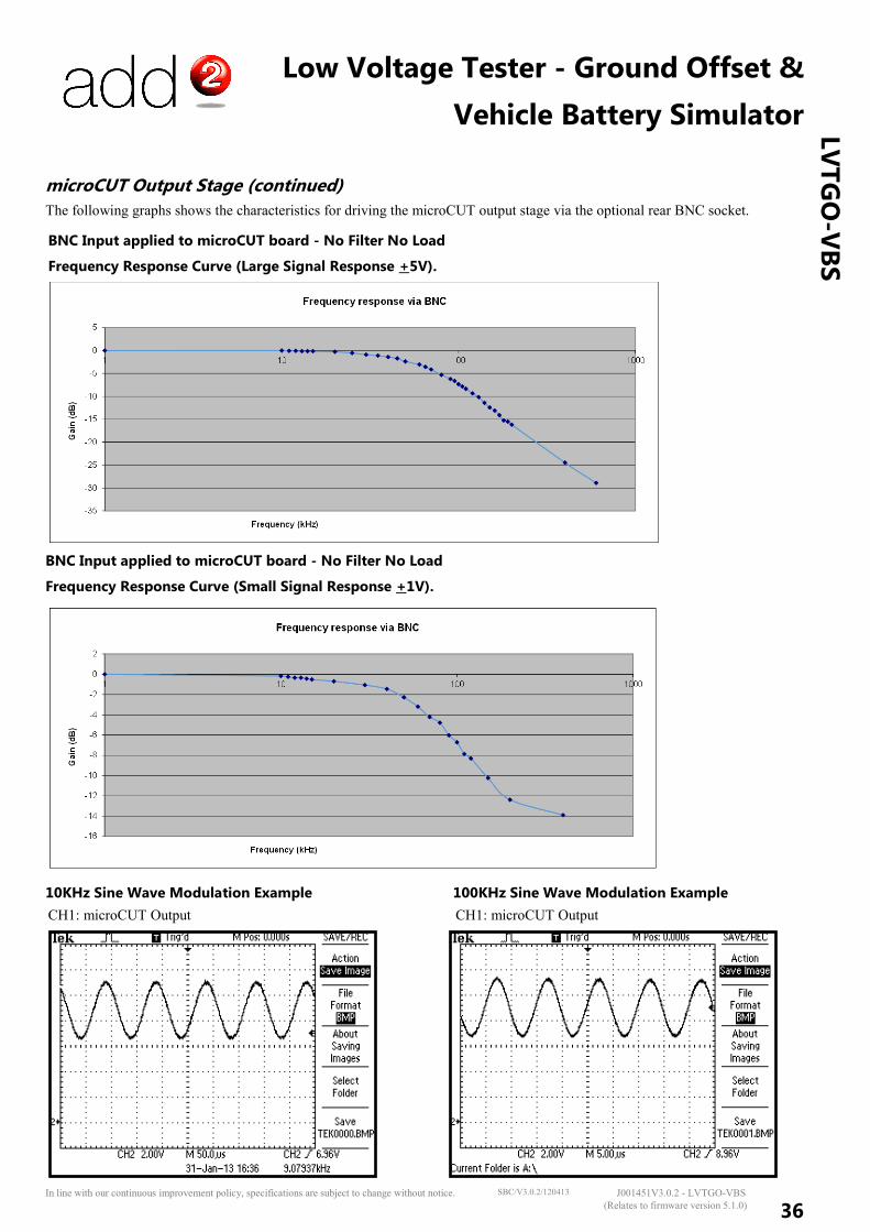
Low Voltage Tester - Ground Offset &
Vehicle Battery Simulator
36
LV
TG
O-V
BS
In line with our continuous improvement policy, specifications are subject to change without notice. J001451V3.0.2 - LVTGO-VBS SBC/V3.0.2/120413
(Relates to firmware version 5.1.0)
microCUT Output Stage (continued)
The following graphs shows the characteristics for driving the microCUT output stage via the optional rear BNC socket.
BNC Input applied to microCUT board - No Filter No Load
Frequency Response Curve (Large Signal Response +5V).
CH1: microCUT Output
BNC Input applied to microCUT board - No Filter No Load
Frequency Response Curve (Small Signal Response +1V).
10KHz Sine Wave Modulation Example
CH1: microCUT Output
100KHz Sine Wave Modulation Example
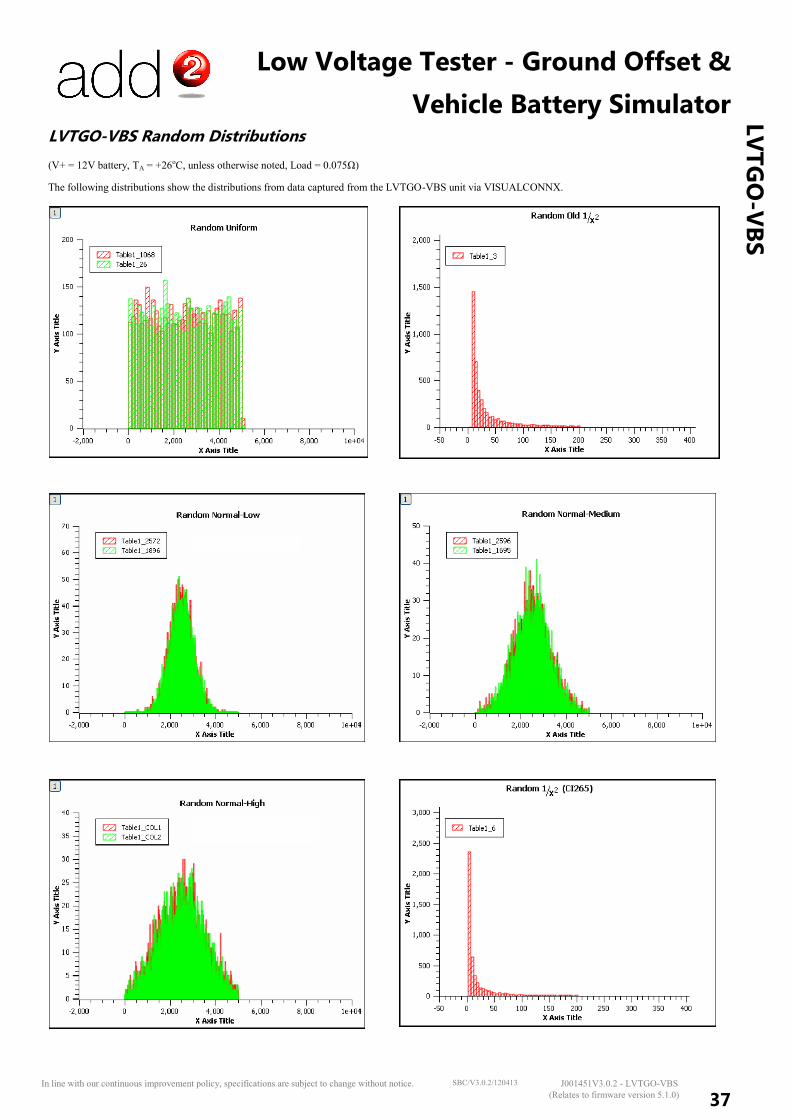
Low Voltage Tester - Ground Offset &
Vehicle Battery Simulator
37
LV
TG
O-V
BS
In line with our continuous improvement policy, specifications are subject to change without notice. J001451V3.0.2 - LVTGO-VBS SBC/V3.0.2/120413
(Relates to firmware version 5.1.0)
LVTGO-VBS Random Distributions
(V+ = 12V battery, TA = +26oC, unless otherwise noted, Load = 0.075Ω)
The following distributions show the distributions from data captured from the LVTGO-VBS unit via VISUALCONNX.
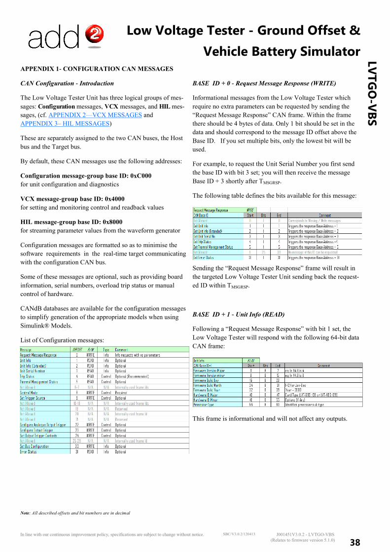
Low Voltage Tester - Ground Offset &
Vehicle Battery Simulator
38
LV
TG
O-V
BS
In line with our continuous improvement policy, specifications are subject to change without notice. J001451V3.0.2 - LVTGO-VBS SBC/V3.0.2/120413
(Relates to firmware version 5.1.0)
APPENDIX 1- CONFIGURATION CAN MESSAGES
CAN Configuration - Introduction
The Low Voltage Tester Unit has three logical groups of mes-
sages: Configuration messages, VCX messages, and HIL mes-
sages, (cf. APPENDIX 2—VCX MESSAGES and
APPENDIX 3– HIL MESSAGES)
These are separately assigned to the two CAN buses, the Host
bus and the Target bus.
By default, these CAN messages use the following addresses:
Configuration message-group base ID: 0xC000
for unit configuration and diagnostics
VCX message-group base ID: 0x4000
for setting and monitoring control and readback values
HIL message-group base ID: 0x8000
for streaming parameter values from the waveform generator
Configuration messages are formatted so as to minimise the
software requirements in the real-time target communicating
with the configuration CAN bus.
Some of these messages are optional, such as providing board
information, serial numbers, overload trip status or manual
control of hardware.
CANdB databases are available for the configuration messages
to simplify generation of the appropriate models when using
Simulink® Models.
List of Configuration messages:
Note: All described offsets and bit numbers are in decimal
BASE ID + 0 - Request Message Response (WRITE)
Informational messages from the Low Voltage Tester which
require no extra parameters can be requested by sending the
“Request Message Response” CAN frame. Within the frame
there should be 4 bytes of data. Only 1 bit should be set in the
data and should correspond to the message ID offset above the
Base ID. If you set multiple bits, only the lowest bit will be
used.
For example, to request the Unit Serial Number you first send
the base ID with bit 3 set; you will then receive the message
Base ID + 3 shortly after TMSGRSP.
The following table defines the bits available for this message:
Sending the “Request Message Response” frame will result in
the targeted Low Voltage Tester Unit sending back the request-
ed ID within TMSGRSP.
BASE ID + 1 - Unit Info (READ)
Following a “Request Message Response” with bit 1 set, the
Low Voltage Tester will respond with the following 64-bit data
CAN frame:
This frame is informational and will not affect any outputs.
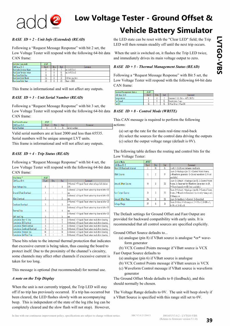
Low Voltage Tester - Ground Offset &
Vehicle Battery Simulator
39
LV
TG
O-V
BS
In line with our continuous improvement policy, specifications are subject to change without notice. J001451V3.0.2 - LVTGO-VBS SBC/V3.0.2/120413
(Relates to firmware version 5.1.0)
BASE ID + 2 - Unit Info (Extended) (READ)
Following a “Request Message Response” with bit 2 set, the
Low Voltage Tester will respond with the following 64-bit data
CAN frame:
This frame is informational and will not affect any outputs.
BASE ID + 3 - Unit Serial Number (READ)
Following a “Request Message Response” with bit 3 set, the
Low Voltage Tester will respond with the following 64-bit data
CAN frame:
Valid serial numbers are at least 2000 and less than 65535.
Serial numbers will be unique amongst LVT units.
This frame is informational and will not affect any outputs.
BASE ID + 4 - Trip Status (READ)
Following a “Request Message Response” with bit 4 set, the
Low Voltage Tester will respond with the following 64-bit data
CAN frame:
These bits relate to the internal thermal protection that indicates
that excessive current is being taken, thus causing the board to
protect itself. Due to the proximity of the channel’s circuitry,
some channels may affect other channels if excessive current is
taken for too long.
This message is optional (but recommended) for normal use.
A note on the Trip Display
When the unit is not currently tripped, the Trip LED will stay
off if no trip has previously occurred. If a trip has occurred but
been cleared, the LED flashes slowly with an accompanying
beep. This is independent of the state of the log (the log can be
completely cleared and the slow flash will not stop). However,
the LED state can be reset with the "Clear LED" field; the Trip
LED will then remain steadily off until the next trip occurs.
When the unit is switched on, it flashes the Trip LED twice,
and immediately drives its main voltage output to zero.
BASE ID + 5 - Thermal Management Status (READ)
Following a “Request Message Response” with Bit 5 set, the
Low Voltage Tester will respond with the following 64-bit data
CAN frame:
BASE ID + 8 - Control Mode (WRITE)
This CAN message is required to perform the following
actions:
(a) set up the rate for the main real-time read-back
(b) select the sources for the control data driving the outputs
(c) select the output voltage range (default is 0V).
The following table defines the routing and control bits for the
Low Voltage Tester:
The Default settings for Ground Offset and Fast Output are
provided for backward compatibility with early units. It is
recommended that all control sources are specified explicitly.
Ground Offset Source defaults to...
(a) analogue (pin 8) if VBatt source is analogue *or* wave-
form generator
(b) VCX Control Points message if VBatt source is VCX
Fast Output Source defaults to
(a) analogue (pin 6) if VBatt source is analogue
(b) VCX Control Points message if VBatt sources is VCX
(c) Waveform Control message if VBatt source is waveform
generator
The Ground Offset Mode defaults to 0 (feedback), and this
should normally be chosen.
The Voltage Range defaults to 0V. The unit will beep slowly if
a VBatt Source is specified with this range still set to 0V.
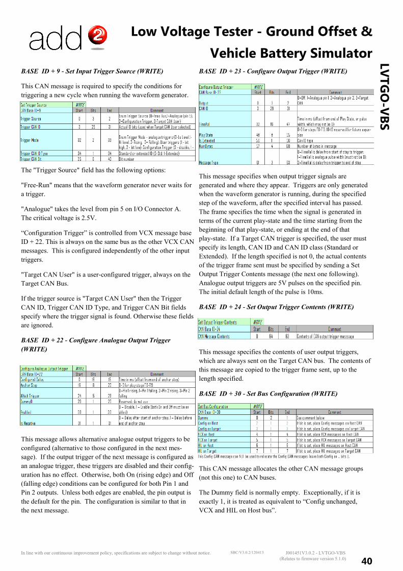
Low Voltage Tester - Ground Offset &
Vehicle Battery Simulator
40
LV
TG
O-V
BS
In line with our continuous improvement policy, specifications are subject to change without notice. J001451V3.0.2 - LVTGO-VBS SBC/V3.0.2/120413
(Relates to firmware version 5.1.0)
BASE ID + 9 - Set Input Trigger Source (WRITE)
This CAN message is required to specify the conditions for
triggering a new cycle when running the waveform generator.
The "Trigger Source" field has the following options:
"Free-Run" means that the waveform generator never waits for
a trigger.
"Analogue" takes the level from pin 5 on I/O Connector A.
The critical voltage is 2.5V.
“Configuration Trigger” is controlled from VCX message base
ID + 22. This is always on the same bus as the other VCX CAN
messages. This is configured independently of the other input
triggers.
"Target CAN User" is a user-configured trigger, always on the
Target CAN Bus.
If the trigger source is "Target CAN User" then the Trigger
CAN ID, Trigger CAN ID Type, and Trigger CAN Bit fields
specify where the trigger signal is found. Otherwise these fields
are ignored.
BASE ID + 22 - Configure Analogue Output Trigger
(WRITE)
This message allows alternative analogue output triggers to be
configured (alternative to those configured in the next mes-
sage). If the output trigger of the next message is configured as
an analogue trigger, these triggers are disabled and their config-
uration has no effect. Otherwise, both On (rising edge) and Off
(falling edge) conditions can be configured for both Pin 1 and
Pin 2 outputs. Unless both edges are enabled, the pin output is
the default for the pin. The configuration is similar to that in
the next message.
BASE ID + 23 - Configure Output Trigger (WRITE)
This message specifies when output trigger signals are
generated and where they appear. Triggers are only generated
when the waveform generator is running, during the specified
step of the waveform, after the specified interval has passed.
The frame specifies the time when the signal is generated in
terms of the current play-state and the time starting from the
beginning of that play-state, or ending at the end of that
play-state. If a Target CAN trigger is specified, the user must
specify its length, CAN ID and CAN ID class (Standard or
Extended). If the length specified is not 0, the actual contents
of the trigger frame sent must be specified by sending a Set
Output Trigger Contents message (the next one following).
Analogue output triggers are 5V pulses on the specified pin.
The initial default length of the pulse is 10ms.
BASE ID + 24 - Set Output Trigger Contents (WRITE)
This message specifies the contents of user output triggers,
which are always sent on the Target CAN bus. The contents of
this message are copied to the trigger frame sent, up to the
length specified.
BASE ID + 30 - Set Bus Configuration (WRITE)
This CAN message allocates the other CAN message groups
(not this one) to CAN buses.
The Dummy field is normally empty. Exceptionally, if it is
exactly 1, it is treated as equivalent to “Config unchanged,
VCX and HIL on Host bus”.
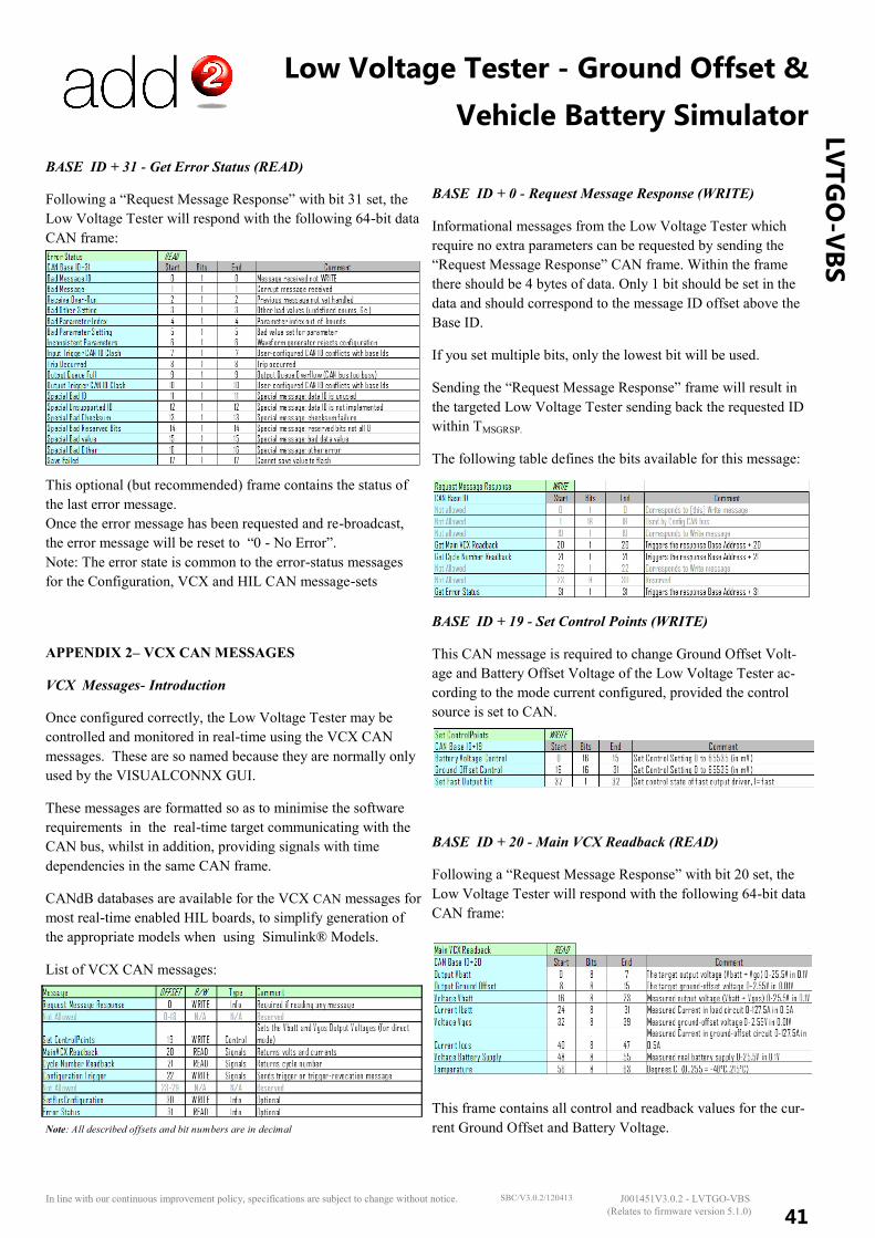
Low Voltage Tester - Ground Offset &
Vehicle Battery Simulator
41
LV
TG
O-V
BS
In line with our continuous improvement policy, specifications are subject to change without notice. J001451V3.0.2 - LVTGO-VBS SBC/V3.0.2/120413
(Relates to firmware version 5.1.0)
BASE ID + 31 - Get Error Status (READ)
Following a “Request Message Response” with bit 31 set, the
Low Voltage Tester will respond with the following 64-bit data
CAN frame:
This optional (but recommended) frame contains the status of
the last error message.
Once the error message has been requested and re-broadcast,
the error message will be reset to “0 - No Error”.
Note: The error state is common to the error-status messages
for the Configuration, VCX and HIL CAN message-sets
APPENDIX 2– VCX CAN MESSAGES
VCX Messages- Introduction
Once configured correctly, the Low Voltage Tester may be
controlled and monitored in real-time using the VCX CAN
messages. These are so named because they are normally only
used by the VISUALCONNX GUI.
These messages are formatted so as to minimise the software
requirements in the real-time target communicating with the
CAN bus, whilst in addition, providing signals with time
dependencies in the same CAN frame.
CANdB databases are available for the VCX CAN messages for
most real-time enabled HIL boards, to simplify generation of
the appropriate models when using Simulink® Models.
List of VCX CAN messages:
Note: All described offsets and bit numbers are in decimal
BASE ID + 0 - Request Message Response (WRITE)
Informational messages from the Low Voltage Tester which
require no extra parameters can be requested by sending the
“Request Message Response” CAN frame. Within the frame
there should be 4 bytes of data. Only 1 bit should be set in the
data and should correspond to the message ID offset above the
Base ID.
If you set multiple bits, only the lowest bit will be used.
Sending the “Request Message Response” frame will result in
the targeted Low Voltage Tester sending back the requested ID
within TMSGRSP.
The following table defines the bits available for this message:
BASE ID + 19 - Set Control Points (WRITE)
This CAN message is required to change Ground Offset Volt-
age and Battery Offset Voltage of the Low Voltage Tester ac-
cording to the mode current configured, provided the control
source is set to CAN.
BASE ID + 20 - Main VCX Readback (READ)
Following a “Request Message Response” with bit 20 set, the
Low Voltage Tester will respond with the following 64-bit data
CAN frame:
This frame contains all control and readback values for the cur-
rent Ground Offset and Battery Voltage.
Low Voltage Tester - Ground Offset &
Vehicle Battery Simulator
42
LV
TG
O-V
BS
In line with our continuous improvement policy, specifications are subject to change without notice. J001451V3.0.2 - LVTGO-VBS SBC/V3.0.2/120413
(Relates to firmware version 5.1.0)
BASE ID + 21 - Cycle Number Readback (READ)
Following a “Request Message Response” with bit 21 set, the
Low Voltage Tester will respond with the following 64-bit data
CAN frame, which can also be streamed.
BASE ID + 22 - Configuration Trigger (WRITE)
This frame is available for use as an input trigger frame, by
enabling the Configuration Trigger using the COM interface.
This is always a “bit high” trigger; a 1 bit sends a trigger, and a
0 bit revokes a pending trigger.
BASE ID + 30 - Set Bus Configuration (WRITE)
This CAN message allocates the other CAN message groups
(not this one) to CAN buses.
BASE ID + 31 - Error Status (READ)
Following a “Request Message Response” with bit 31 set, the
Low Voltage Tester will respond with the following 64-bit data
CAN frame:
For more details cf. Appendix 1: Get Error Status)
APPENDIX 3– HIL CAN MESSAGES
HIL Messages - Introduction
Real-time interactions with the target are normally carried on
the Target CAN bus. User-configured triggers are always on
the Target CAN bus. Other, pre-defined messages which are
provided for the user’s real-time interaction with the target are
put in the HIL message group, which is allocated to the Target
CAN bus by default.
To minimise traffic which the user may have to handle, this
message group is not used to carry error frames. They are re-
ported in one of the other message groups instead, by prefer-
ence one which is not assigned to the Target CAN bus.
List of HIL CAN messages:
Note: All described offsets and bit numbers are in decimal
BASE ID + 17 - Control Parameters Echo (WRITE)
This message is used when the waveform generator is running,
to specify how parameter values used in the current cycle are to
be returned. Because parameter values may be randomised,
reading the parameter settings is not enough to determine the
values used at a particular time.
There are two ways to use it, specified by the contents of the
“Echo Control Polling” and “Echo Control Streaming” fields.
Setting the contents of the field “Echo Control Polling” to 1
configures the values specified to be returned when next re-
quested: otherwise they are ignored. Setting the field “Echo
Control Streaming” to 1 starts streaming of parameters as they
are generated, and setting it to 0 stops streaming.
The A and B specifiers merely allow two different parameters
to be polled at once. As a special case, polling for a value with
Type Bits=15 and Parameter Index=15 is a dummy operation.
This combination is guaranteed never to correspond to a
parameter in use.
Low Voltage Tester - Ground Offset &
Vehicle Battery Simulator
43
LV
TG
O-V
BS
In line with our continuous improvement policy, specifications are subject to change without notice. J001451V3.0.2 - LVTGO-VBS SBC/V3.0.2/120413
(Relates to firmware version 5.1.0)
BASE ID + 18 - Parameters Echo (READ)
This is a response to a Get Parameters Echo frame (Base ID +
20) when polling, or it is streamed as requested in the Control
Parameters Echo frame (Base ID + 17). It contains the values
specified, as far as possible.
Requests for parameter values which are not currently in use
are honoured: the most recently generated value is returned.
If a request is made for a parameter that is not supported in the
firmware then it is echoed as a dummy entry, with Type bits 15
and Parameter Index 15. This also allows an odd parameter left
over at the end of a cycle to be streamed without waiting for the
next cycle to begin.
BASE ID + 19 - Set Control Points (WRITE)
This CAN message is required to change Ground Offset Volt-
age and Battery Offset Voltage of the Low Voltage Tester ac-
cording to the mode current configured, provided the control
source is set to CAN.
BASE ID + 20 - Get Parameters Echo (WRITE)
This empty CAN message is used to direct the LVTGO-VBS to
send a polled parameter message (Base ID + 18) as specified in
the previous Control Parameters Echo message (Base ID + 17).
BASE ID + 30 - Set Bus Configuration (WRITE)
This CAN message allocates the other CAN message groups
(not this one) to CAN buses.
Low Voltage Tester - Ground Offset &
Vehicle Battery Simulator
44
LV
TG
O-V
BS
In line with our continuous improvement policy, specifications are subject to change without notice. J001451V3.0.2 - LVTGO-VBS SBC/V3.0.2/120413
(Relates to firmware version 5.1.0)
APPENDIX 4– TROUBLESHOOTING LVT ISSUES
CAN Driver
Ensure you have installed and selected (via the “Connection
Settings” menu ) the CAN card you are using.
CAN Connection
Ensure you connect the GUI (VISUALCONNX) CAN lead to
the one marked ‘HOST’.
Minimum Load
If using a MK1 LVT with B and C outputs you must provide a
minimum load of around 50Ω to pull the output to 0V / Ground
Offset as required.
If using aMK2 LVT with A, B and C outputs you must provide
a minimum load of around 500Ω to pull the output to 0V /
Ground Offset as required.
Apparent Trips
Starting with V3.0.0 of the firmware, behaviour very similar to
a trip occurs if the application connects and sets the operating
mode without setting the output range, The VB OUT pin is
driven to 0V, and the trip LED flashes at 0.5Hz with a 25%
duty cycle, indicating that the firmware is holding the VBatt
voltage at zero.
Other Apparent Trips
There is yet another way in which the outputs can be forced to
zero, which is again not a trip, and this time has no effect on
the Trip LED. Recent versions of the firmware, starting with
Version 5.1.0, check the firmware against the actual hardware
of the LVTGO-VBS unit, and shut down the outputs in case of
inconsistency. This is reported to the GUI as 'Bad Firmware
Version' on the Error Status and Special Values form. This is a
check for errors during manufacturing, and customers should
not see it. If the problem persists after power-cycling the LVT-
GO-VBS and re-starting the GUI, the unit must be returned to
add2.
Low Voltage Tester - Ground Offset &
Vehicle Battery Simulator
45
LV
TG
O-V
BS
In line with our continuous improvement policy, specifications are subject to change without notice. J001451V3.0.2 - LVTGO-VBS SBC/V3.0.2/120413
(Relates to firmware version 5.1.0)
APPENDIX 4– LOW VOLTAGE TESTER GUI SCREEN SHOTS AND OUTPUT TRACES
Example of Cranking waveform
Example of Ramp Up and Down waveform
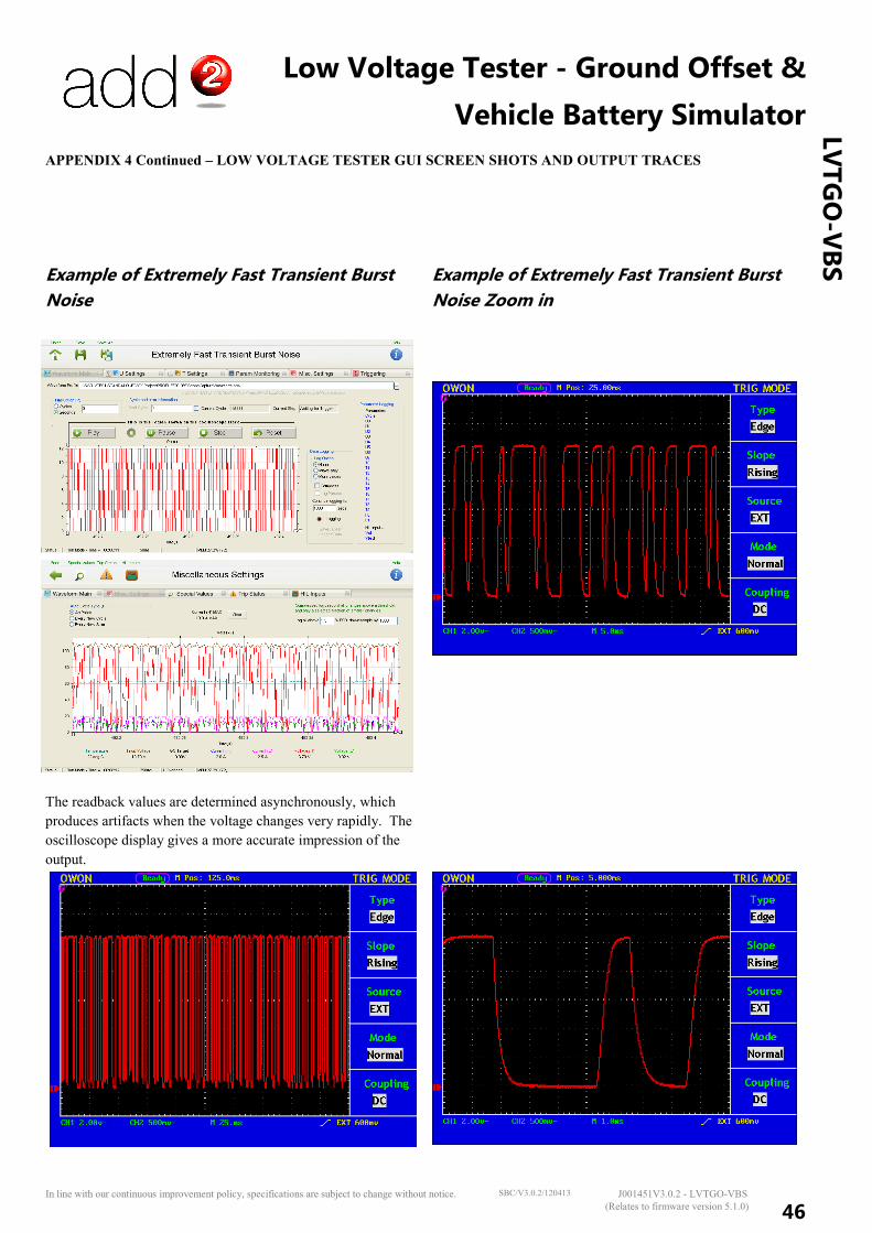
Low Voltage Tester - Ground Offset &
Vehicle Battery Simulator
46
LV
TG
O-V
BS
In line with our continuous improvement policy, specifications are subject to change without notice. J001451V3.0.2 - LVTGO-VBS SBC/V3.0.2/120413
(Relates to firmware version 5.1.0)
Example of Extremely Fast Transient Burst
Noise
Example of Extremely Fast Transient Burst
Noise Zoom in
The readback values are determined asynchronously, which
produces artifacts when the voltage changes very rapidly. The
oscilloscope display gives a more accurate impression of the
output.
APPENDIX 4 Continued – LOW VOLTAGE TESTER GUI SCREEN SHOTS AND OUTPUT TRACES
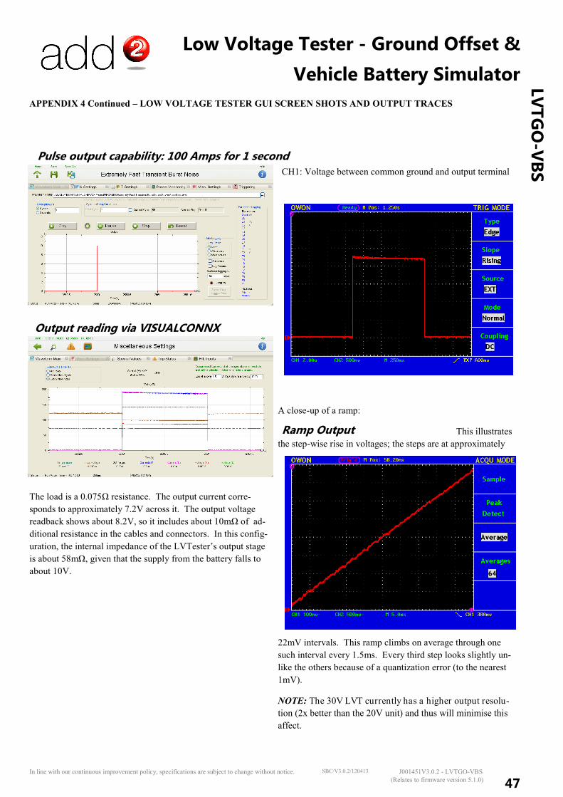
Low Voltage Tester - Ground Offset &
Vehicle Battery Simulator
47
LV
TG
O-V
BS
In line with our continuous improvement policy, specifications are subject to change without notice. J001451V3.0.2 - LVTGO-VBS SBC/V3.0.2/120413
(Relates to firmware version 5.1.0)
The load is a 0.075Ω resistance. The output current corre-
sponds to approximately 7.2V across it. The output voltage
readback shows about 8.2V, so it includes about 10mΩ of ad-
ditional resistance in the cables and connectors. In this config-
uration, the internal impedance of the LVTester’s output stage
is about 58mΩ, given that the supply from the battery falls to
about 10V.
A close-up of a ramp:
This illustrates
the step-wise rise in voltages; the steps are at approximately
22mV intervals. This ramp climbs on average through one
such interval every 1.5ms. Every third step looks slightly un-
like the others because of a quantization error (to the nearest
1mV).
NOTE: The 30V LVT currently has a higher output resolu-
tion (2x better than the 20V unit) and thus will minimise this
affect.
Pulse output capability: 100 Amps for 1 second
Output reading via VISUALCONNX
CH1: Voltage between common ground and output terminal
Ramp Output
APPENDIX 4 Continued – LOW VOLTAGE TESTER GUI SCREEN SHOTS AND OUTPUT TRACES