Embed Size (px)
Citation preview

588 JOURNAL OF MICROELECTROMECHANICAL SYSTEMS, VOL. 18, NO. 3, JUNE 2009
Low-Temperature Monolithic Encapsulation UsingPorous-Alumina Shell Anodized on Chip
Rihui He and Chang-Jin Kim
Abstract—A thin-film encapsulation process, featuring low-temperature steps, hermetic sealing (preliminary), and RF-compatible shell, is reported. Uniquely attractive as comparedwith the existing MEMS packaging approaches is its capability tomonolithically package metal microstructures inside a microcavityon chip in one continuous surface-micromachining process. Thekey for this process is a technique to fabricate a large freestandingporous membrane on chip by postdeposition anodization of thin-film aluminum at room temperature. The porous-alumina mem-brane allows for the diffusion of gas or liquid etchants throughthe nanopores to etch away the sacrificial material underneath,freeing the movable microstructures encapsulated inside the cav-ity. To seal the package, a thin film is deposited over the alu-mina shell whose nanoscale pores of a high aspect ratio (> 30)do not allow any detectable penetration of the sealing mater-ial. The low-temperature (< 300 ◦C) encapsulation process pro-duced a low-pressure seal (8 torr), monitored by a Pirani pressuregauge that also represents an encapsulated freestanding metalmicrostructure in the cavity. The thin-film package demonstrateda considerably low RF insertion loss of less than 0.1 dB up to40 GHz. [2007-0267]
Index Terms—Integrated packaging, low temperature, mono-lithic encapsulation, porous alumina, RF MEMS packaging, thin-film encapsulation.
I. INTRODUCTION
COMPARED to conventional approaches of packaging anindividual MEMS device in metal or ceramic packages,
wafer-level packaging—packaging the delicate MEMS deviceson wafer before dicing—has long been accepted as the mosteffective way to reduce the back-end-of-line cost for a MEMSproduct. Hybrid wafer bonding [1]–[7], which employs directsurface bonding or an intermediate material to bond a sepa-rate capping wafer to the device wafer, is widely available inthe industry as a mature wafer-level packaging approach. Toaddress the main drawbacks in hybrid wafer bonding, such asexcessive seal ring width, a thick profile, and the burden ofaligning two wafers, various monolithic thin-film encapsula-
Manuscript received November 4, 2007; revised May 5, 2008, September 5,2008, December 8, 2008, and February 22, 2009. First published April 24,2009; current version published June 3, 2009. This work was supportedby the DARPA Harsh Environment Robust Micromechanical Technology(HERMIT) Program. Subject Editor L. Spangler.
R. He was with the Department of Mechanical and Aerospace Engineering,University of California, Los Angeles, CA 90095 USA. He is now withQualcomm MEMS Technologies, Inc., San Jose, CA 95134 USA (e-mail: [email protected]).
C.-J. Kim is with the Department of Mechanical and Aerospace Engineering,University of California, Los Angeles, CA 90095 USA.
Color versions of one or more of the figures in this paper are available onlineat http://ieeexplore.ieee.org.
Digital Object Identifier 10.1109/JMEMS.2009.2017088
tion processes [8]–[20] have been demonstrated, among whichepitaxial silicon encapsulation is being used in commercialMEMS resonator products (www.sitime.com). Using thin-filmprocesses, a sacrificial layer is deposited over an unreleaseddevice, followed by the deposition of a thin film on top to forman encapsulation shell layer. Through etch holes opened in theencapsulation shell by lithography, the sacrificial materials areselectively removed by wet or dry etching, creating a cavityand freeing microstructures in it. The cavity is finally sealedby deposition of a micrometer- to several-micrometer-thick thinfilm on the encapsulation shell.
Permeable polysilicon, in situ deposited by low-pressurechemical-vapor deposition (LPCVD) under a certain condition[10], [13], and porous polysilicon, formed by postdepositionelectrochemical etching [18], [20], were demonstrated as en-capsulation shell materials with numerous submicrometer etchholes. The use of porous encapsulation shell allowed for fastremoval of the sacrificial layers over the entire cavity areaand lessened the issue of the internal deposition of the sealingmaterial during the sealing process. Inspired by the success of aporous polysilicon shell in [13], we develop a new nanoporousthin film in this paper to meet with two essential requirementsof packaging RF MEMS devices—low temperature and lowRF loss. Low-temperature thin-film encapsulation has beendemonstrated by using evaporated Al as a sealing film [21] orelectroplated Ni as a package shell [16]. However, they are notsuitable for RF packaging, as a conductive metal package intro-duces an RF loss path through the package. Dielectric materialsdeposited by sputtering [17] or plasma-enhanced chemical-vapor deposition (PECVD) [22] and spin-on glass [17] wereused to package RF switches, and such packages showed RFlosses much less than those of the conventional wafer bondingusing solder [23], polymer bonding [24], or thermocompres-sion [25]–[27].
Noting that aluminum can be deposited at a low temperatureand that it can be anodized to a dielectric material of aluminawith directional nanopores in a similar way as polysilicon[20], we have developed a process to form a freestandingporous-alumina membrane through postdeposition anodizationfor thin-film encapsulation [28] and reported some initial resultsin [29]. A similar method for fabricating a freestanding porous-alumina membrane for MEMS packaging was reported in arecent paper [30], where a different etching technique was usedto form a porous-alumina membrane. Here, we consolidate theincremental results reported in [28] and [29]. Possessing thebenefits of nanoporous thin-film encapsulation [20] and featur-ing a low-temperature process and extremely low RF loss, the
1057-7157/$25.00 © 2009 IEEE
Authorized licensed use limited to: Univ of Calif Los Angeles. Downloaded on June 8, 2009 at 17:36 from IEEE Xplore. Restrictions apply.

HE AND KIM: MONOLITHIC ENCAPSULATION USING POROUS-ALUMINA SHELL ANODIZED ON CHIP 589
Fig. 1. Schematic of the pore structure of porous alumina. The pore structureis a hexagonal array of cylindrical pores, with pore diameter ranging from 10to 300 nm. An alumina barrier layer is present at the bottom of the pores,preventing them from growing through the thickness.
porous-alumina thin-film encapsulation process developed inthis paper is potential to be a cost-effective packaging solutionfor various MEMS devices, particularly RF devices.
II. DESIGN AND FABRICATION
A. Fabrication of Porous-Alumina Membrane
Porous alumina is usually obtained by anodizing bulk alu-minum foils in a variety of acidic electrolytes such as phos-phoric acid, sulfuric acid, and oxalic acid. The typical porestructure, shown schematically in Fig. 1, is a hexagonal arrayof cylindrical pores (pore diameter: 10–300 nm) with a bot-tom Al2O3 barrier layer. In a typical (including commercial)porous-alumina process, the barrier layer is removed by pol-ishing. For our application, however, the bottom Al2O3 barrierlayer needs to be removed during the monolithic fabricationprocess to allow the etchants to diffuse through the nanoporesand etch away the sacrificial material underneath. Because thewall thickness between the alumina pores is roughly twice thethickness of the barrier layer, removing the barrier layer byisotropic etching would also remove most of the alumina porewall. Progressively reducing the anodization voltage [31], [32],or reversing the bias voltage immediately after the completionof the anodization etching of Al [33], requires accurate timingcontrol to stop the etching and is not a reliable process forfabricating a porous-alumina membrane out of aluminum thinfilm deposited on a partially processed wafer surface.
It is possible to remove the barrier layer but not the aluminapore wall if the aluminum thin film is deposited on anotherconductive layer. When anodizing the Al thin film depositedon a silicon substrate [34] or an ITO-coated glass substrate[35], the conductive seed layer (silicon or ITO) allowed theanodization to continue, even after the etching front reached theinterface, turning the entire Al thin film into porous alumina andtransforming the otherwise thick and attached barrier layer intonumerous thin arches. These thin arches can be removed by anisotropic wet etchant while only widening the pores marginally.Using a similar technique, we added a seed layer before thealuminum deposition and successfully perforated the bottombarrier layer in situ.
A process flow for fabricating the porous-alumina membraneis shown in Fig. 2. A stack of thin films on a silicon substrate,from the bottom to the top, consisted of a 0.3-μm PECVDoxide layer for insulation, a 1.5-μm amorphous-silicon (a-Si)sacrificial layer, a 1000/100-Å evaporated Ti/Au layer. and a
Fig. 2. Fabrication process flow of a porous-alumina membrane. Anodizationetching was performed at step (b). The pore morphology change of porousalumina during anodization etching is shown in Fig. 5 (only the box area definedby dashed lines in (b) is displayed).
Fig. 3. Schematic view of the anodization etching setup.
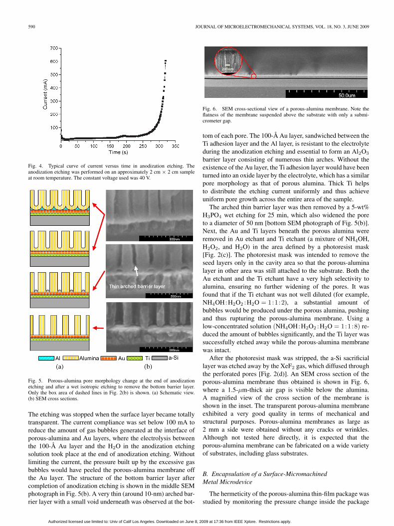
1-μm evaporated Al layer [Fig. 2(a)]. After being diced into2-cm × 2-cm pieces, the samples were placed in a simplecustom-made setup (Fig. 3) and anodized at a 40-V constantbias in a 0.3-mol/L oxalic acid at room temperature [Fig. 2(b)].Although the anodization was done at the chip level in thispaper, the same process can be scaled up to the wafer level oncethe challenge of keeping the anodization etching uniform acrossthe wafer is overcome. Fig. 4 shows a typical current variationover time during the anodization etching. During the anodiza-tion etching, the current stabilized for a long period, indicatinga process of stable pore growth. The pore morphology at the endof this stage can be observed from an SEM cross section shownat the top in Fig. 5(b). As the etching continues, the currentstarted to increase rapidly, and it was accompanied with gasbubble generation, signifying that the etching front has reachedthe Au layer where electrolysis would occur. At the same time,the color of the surface started to change from opaque (i.e., thecolor of aluminum) to translucent and, finally, to transparent.
Authorized licensed use limited to: Univ of Calif Los Angeles. Downloaded on June 8, 2009 at 17:36 from IEEE Xplore. Restrictions apply.
590 JOURNAL OF MICROELECTROMECHANICAL SYSTEMS, VOL. 18, NO. 3, JUNE 2009
Fig. 4. Typical curve of current versus time in anodization etching. Theanodization etching was performed on an approximately 2 cm × 2 cm sampleat room temperature. The constant voltage used was 40 V.
Fig. 5. Porous-alumina pore morphology change at the end of anodizationetching and after a wet isotropic etching to remove the bottom barrier layer.Only the box area of dashed lines in Fig. 2(b) is shown. (a) Schematic view.(b) SEM cross sections.
The etching was stopped when the surface layer became totallytransparent. The current compliance was set below 100 mA toreduce the amount of gas bubbles generated at the interface ofporous-alumina and Au layers, where the electrolysis betweenthe 100-Å Au layer and the H2O in the anodization etchingsolution took place at the end of anodization etching. Withoutlimiting the current, the pressure built up by the excessive gasbubbles would have peeled the porous-alumina membrane offthe Au layer. The structure of the bottom barrier layer aftercompletion of anodization etching is shown in the middle SEMphotograph in Fig. 5(b). A very thin (around 10-nm) arched bar-rier layer with a small void underneath was observed at the bot-
Fig. 6. SEM cross-sectional view of a porous-alumina membrane. Note theflatness of the membrane suspended above the substrate with only a submi-crometer gap.
tom of each pore. The 100-Å Au layer, sandwiched between theTi adhesion layer and the Al layer, is resistant to the electrolyteduring the anodization etching and essential to form an Al2O3
barrier layer consisting of numerous thin arches. Without theexistence of the Au layer, the Ti adhesion layer would have beenturned into an oxide layer by the electrolyte, which has a similarpore morphology as that of porous alumina. Thick Ti helpsto distribute the etching current uniformly and thus achieveuniform pore growth across the entire area of the sample.
The arched thin barrier layer was then removed by a 5-wt%H3PO4 wet etching for 25 min, which also widened the poreto a diameter of 50 nm [bottom SEM photograph of Fig. 5(b)].Next, the Au and Ti layers beneath the porous alumina wereremoved in Au etchant and Ti etchant (a mixture of NH4OH,H2O2, and H2O) in the area defined by a photoresist mask[Fig. 2(c)]. The photoresist mask was intended to remove theseed layers only in the cavity area so that the porous-aluminalayer in other area was still attached to the substrate. Both theAu etchant and the Ti etchant have a very high selectivity toalumina, ensuring no further widening of the pores. It wasfound that if the Ti etchant was not well diluted (for example,NH4OH :H2O2 :H2O = 1:1:2), a substantial amount ofbubbles would be produced under the porous alumina, pushingand thus rupturing the porous-alumina membrane. Using alow-concentrated solution (NH4OH :H2O2 :H2O = 1:1:8) re-duced the amount of bubbles significantly, and the Ti layer wassuccessfully etched away while the porous-alumina membranewas intact.
After the photoresist mask was stripped, the a-Si sacrificiallayer was etched away by the XeF2 gas, which diffused throughthe perforated pores [Fig. 2(d)]. An SEM cross section of theporous-alumina membrane thus obtained is shown in Fig. 6,where a 1.5-μm-thick air gap is visible below the alumina.A magnified view of the cross section of the membrane isshown in the inset. The transparent porous-alumina membraneexhibited a very good quality in terms of mechanical andstructural purposes. Porous-alumina membranes as large as2 mm a side were obtained without any cracks or wrinkles.Although not tested here directly, it is expected that theporous-alumina membrane can be fabricated on a wide varietyof substrates, including glass substrates.
B. Encapsulation of a Surface-MicromachinedMetal Microdevice
The hermeticity of the porous-alumina thin-film package wasstudied by monitoring the pressure change inside the package
Authorized licensed use limited to: Univ of Calif Los Angeles. Downloaded on June 8, 2009 at 17:36 from IEEE Xplore. Restrictions apply.

HE AND KIM: MONOLITHIC ENCAPSULATION USING POROUS-ALUMINA SHELL ANODIZED ON CHIP 591
Fig. 7. Process flow for porous-alumina encapsulation of a Pt Pirani gauge.
through an encapsulated metal Pirani gauge. The Pirani gaugeis a freestanding surface-micromachined device and serves torepresent a typical surface-micromachined metal structure andto read the vacuum level in situ. The use of Pirani gauge tomonitor the pressure in situ was introduced in [7]–[9] and [16],and a polysilicon Pirani gauge has successfully been utilized forpolysilicon encapsulation in [20].
The process flow is shown in Fig. 7. First, a 6000-Å siliconoxide was deposited by PECVD on a silicon substrate forinsulation purposes. Then, a 1-μm a-Si layer was depositedby PECVD, serving as the sacrificial layer between the Piranigauge and the substrate [Fig. 7(a)]. Next, the Pirani gaugewas fabricated by sandwiching 100/400/100-Å Cr/Pt/Cr metallayers between two layers of 3000-Å low-stress PECVD ox-ide [Fig. 7(c)], through which release holes were opened byreactive ion etching. Next, a 4-μm photoresist (AZP 4330)sacrificial layer was deposited and patterned to define the gapbetween the Pirani gauge and the thin-film encapsulation layersdeposited afterward [Fig. 7(d)]. To reduce the outgassing duringthe subsequent processes, the photoresist was hard baked at120 ◦C in an oven for 20 min, followed by an O2 plasma etchingfor 2 min to roughen the surface and improve the adhesion ofmetal layers subsequently deposited. The thin-film shell abovethe photoresist sacrificial layer consisted of sputtered 3200-ÅTi layer and evaporated 100/15000-Å Au/Al layer [Fig. 7(e)].Then, the anodization etching of Al was performed on a2-cm × 2-cm chip [Fig. 7(f)].
Next, using a photoresist mask, the alumina pores in the cav-ity area were widened in 5-wt% H3PO4 etching for 25 min, andthe Ti/Au seed layers were also removed through the pores byTi and Au etchants. The photoresist mask, along with the pho-toresist sacrificial layer below the porous alumina, was removedby O2 plasma etching [Fig. 7(g)]. Afterward, the a-Si sacrificiallayer under the Pirani gauge was removed by XeF2 plasmadry etching.
The sealing of the package was achieved by depositing aPECVD low-stress nitride of 2.5 μm at 300 ◦C. The depositionpressure was 500 mtorr. The thickness of the sealing Si3N4 filmwas chosen to prevent physical contact between the packageshell and the Pirani gauge when the package shell is deflectedby the pressure difference as high as ∼1 atm after sealing. Thepressure–deflection relationship [36], [37] is given as
p =3.41σth
a2+
2.45Eth3
a4(1)
where p is the pressure difference applied on the shell; t,2a, and h are the thickness, width, and deflection of theshell, respectively; E is the effective Young’s modulus of thepackage shell, which is dominated by that of sealing Si3N4
(∼190 GPa). Neglecting the residual stress (i.e., σ = 0) andassuming that the pressure inside the sealed cavity is 0.5 torr(= PECVD deposition pressure), we estimate that a 2.5-μm-thick Si3N4 shell that is 200 μm on a side would deflect around1.9 μm. This deflection is smaller than the thickness (4 μm)of the photoresist sacrificial layer with a safety margin of two,ensuring that the spacing between the shell and the Pirani gaugeis enough under reasonable operation conditions.
Then, the contact pads were opened to obtain electric con-nection to the Pirani gauge [Fig. 7(h)]. Note that the highesttemperature in the current process was the deposition temper-ature of the sacrificial and sealing layers by PECVD. If theywere deposited at a lower temperature, the thermal budget forthe entire process would be determined merely by the litho-graphic steps.
C. RF Performance of a Porous-Alumina Thin-Film Package
Unlike the lithographically defined etch holes [8], [9], [11],[12], [14], [15], [17], [19], the nanopores with a very highaspect ratio in this paper do not allow the sealing material
Authorized licensed use limited to: Univ of Calif Los Angeles. Downloaded on June 8, 2009 at 17:36 from IEEE Xplore. Restrictions apply.

592 JOURNAL OF MICROELECTROMECHANICAL SYSTEMS, VOL. 18, NO. 3, JUNE 2009
Fig. 8. Test process to detect the penetration of the sealing material through porous alumina. To remove the native oxide, the silicon substrate was cleanedby hydrofluoric acid before the Ti deposition. The oxide deposition was performed in PECVD. The porous-alumina layer of two thicknesses (0.5 and 1.0 µm)was tested.
Fig. 9. Process flow for porous-alumina encapsulation of a CPW line.
to pass through them, effectively preventing its depositioninside the cavity. It was studied experimentally in [14] thatthe amount of sealing material (PECVD thin film) depositedinside the cavity was dependent on the aspect ratio of therelease holes. The authors concluded that no internal depositionof the sealing material would occur if the aspect ratio (i.e.,depth to diameter) of the release holes remains above fourwhen the release holes are 0.35 μm in diameter. Given that anaspect ratio over ten (e.g., 0.5-μm-thick porous alumina withpores of diameter below 50 nm) can be easily obtained forthe pores of porous alumina, it is anticipated that no sealingmaterial would diffuse through the pores and deposit on thedevice surface inside the package. An experiment was carriedout to confirm our claim. The test sample has a configuration,as shown in Fig. 8(a). The porous-alumina cavity was formedon a silicon substrate by removing the 5000-Å Ti sacrifi-cial layer through the nanopores. Porous-alumina membranesof two different thicknesses, namely, 5000 Å and 1.5 μm,were fabricated. A pore aspect ratio ranging from 10 to 25 wasobtained by changing the pore size through controlling the timein the widening process of the pores in 5-wt% H3PO4. Afterbeing sealed by a 5000-Å PECVD oxide deposition, as shownFig. 8(b), the cavity was ruptured using a probe tip, and thethickness of oxide on top of the silicon substrate inside thecavity was measured by Nanospec with a thin oxide program(low limit: 20 Å). For all the samples tested, a “less than
20-Å” result was obtained, indicating that the porous-aluminashell effectively prevented the internal deposition of the sealingmaterial during the sealing process.
To investigate the RF performance of the porous-aluminathin-film package, a coplanar waveguide (CPW) device was fab-ricated and packaged, following the fabrication process shownin Fig. 9. The process starts with 6000-Å thermal oxidation, aswell as 3000-Å LPCVD silicon nitride deposition, to insulatethe CPW line from the substrate [Fig. 9(a)]. A silicon waferwith high resistivity (> 2000 Ω · cm) was chosen to reduce theRF loss through the substrate. The subsequent liftoff process ofCr/Au 200/8000 Å formed a CPW line [Fig. 9(b)]. The dimen-sion of CPW lines was designed and simulated using a commer-cial software (HFSS). The next step was PECVD depositions of1-μm SiO2 and 1.8-μm a-Si sacrificial layer [Fig. 9(c)]. Then, a1000/100-Å Ti/Au seed layer was evaporated and patterned bythe liftoff process [Fig. 9(d)], followed by 1-μm Al evaporation[Fig. 9(e)]. The wafer was diced into chips with a size ofaround 2 cm × 2 cm. Following the procedure described earlier,the Al thin film on the entire chip was turned into porousalumina by the anodization etching [Fig. 9(f)], and the porous-alumina cavity was formed by removing the Ti/Au seed layerand the a-Si sacrificial layer sequentially [Fig. 9(g)]. A PECVDdeposition of 1-μm low-stress silicon nitride sealed the device[Fig. 9(h)]. The final step was etching away all the films aboveAu in the electrical contact area.
Authorized licensed use limited to: Univ of Calif Los Angeles. Downloaded on June 8, 2009 at 17:36 from IEEE Xplore. Restrictions apply.
HE AND KIM: MONOLITHIC ENCAPSULATION USING POROUS-ALUMINA SHELL ANODIZED ON CHIP 593
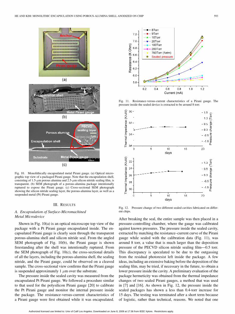
Fig. 10. Monolithically encapsulated metal Pirani gauge. (a) Optical micro-graphic top view of a packaged Pirani gauge. Note that the encapsulation shell,consisting of 1.5-µm porous alumina and 2.5-µm silicon nitride sealing film, istransparent. (b) SEM photograph of a porous-alumina package intentionallyruptured to expose the Pirani gauge. (c) Cross-sectional SEM photographshowing the silicon nitride sealing layer, the porous-alumina layer, as well as asuspended metal (Pt) Pirani gauge.
III. RESULTS
A. Encapsulation of Surface-MicromachinedMetal Microdevice
Shown in Fig. 10(a) is an optical microscope top view of thepackage with a Pt Pirani gauge encapsulated inside. The en-capsulated Pirani gauge is clearly seen through the transparentporous-alumina shell and silicon nitride seal. From the angledSEM photograph of Fig. 10(b), the Pirani gauge is shownfreestanding after the shell was intentionally ruptured. Fromthe SEM photograph of Fig. 10(c), the cross-sectional detailsof all the layers, including the porous-alumina shell, the sealingnitride, and the Pirani gauge, could be observed on a cleavedsample. The cross-sectional view confirms that the Pirani gaugeis suspended approximately 1 μm over the substrate.
The pressure inside the sealed cavity was measured from theencapsulated Pt Pirani gauge. We followed a procedure similarto that used for the polysilicon Pirani gauge [20] to calibratethe Pt Pirani gauge and monitor the internal pressure insidethe package. The resistance-versus-current characteristics ofa Pirani gauge were first obtained while it was encapsulated.
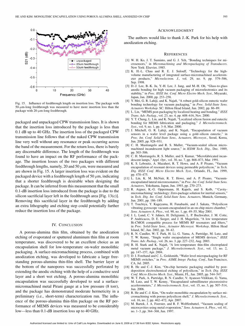
Fig. 11. Resistance-versus-current characteristics of a Pirani gauge. Thepressure inside the sealed device is extracted to be around 8 torr.
Fig. 12. Pressure change of two different sealed cavities fabricated on differ-ent chips.
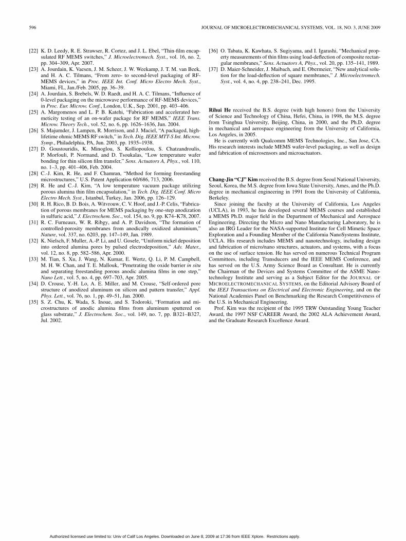
After breaking the seal, the entire sample was then placed in apressure-controlling chamber, where the gauge was calibratedagainst known pressures. The pressure inside the sealed cavity,extracted by matching the resistance–current curve of the Piranigauge while sealed with the calibration data (Fig. 11), wasaround 8 torr, a value that is much larger than the depositionpressure of the PECVD silicon nitride sealing film—0.5 torr.This discrepancy is speculated to be due to the outgassingfrom the residual photoresist left inside the package. A fewideas, including an extensive baking before the deposition of thesealing film, may be tried, if necessary in the future, to obtain alower pressure inside the cavity. A preliminary evaluation of thepackage hermeticity was obtained from the thermal impedancechanges of two sealed Pirani gauges, a method that was usedin [7] and [16]. As shown in Fig. 12, the pressure inside thesealed packages has shown a less than 0.4-torr increase for15 days. The testing was terminated after a short term becauseof logistic, rather than technical, reasons. We noted that one
Authorized licensed use limited to: Univ of Calif Los Angeles. Downloaded on June 8, 2009 at 17:36 from IEEE Xplore. Restrictions apply.

594 JOURNAL OF MICROELECTROMECHANICAL SYSTEMS, VOL. 18, NO. 3, JUNE 2009
Fig. 13. Encapsulated CPW device. The Au signal line is clearly visible through the transparent porous-alumina shell in (a). Schematic cross-sectional views areshown in (b) and (c). The a-Si, left to serve as electric feedthrough, turns out to be the main source of RF insertion loss.
of the devices showed a pressure decrease inside the cavityafter 12 days. This could be due to the fluctuation of ambienttemperature as the performance of the Pirani gauge is sensitiveto the temperature change. Another possible reason is that theoutgass from the traces of photoresist became absorbed on theinterior surface of the porous alumina. A long-term hermeticitystudy of varying device configurations is desired in the future.
B. RF Performance of a Porous-Alumina Thin-Film Package
An optical microscopic top view of a fabricated devicefor evaluating the RF performance is shown in Fig. 13(a). A160-μm × 300-zμm sealed cavity is seen in the middle of thephotograph. The Au signal line encapsulated inside the sealedcavity is clearly visible through the transparent encapsulationshell, which is composed of 1.2-μm porous alumina and 1-μmsilicon nitride thin films. The schematic views of the crosssection of the devices along the A−A′ and B−B′ directionare shown in Fig. 13(b) and (c), respectively. The SEM crosssection in Fig. 13(b) shows the porous alumina, along withthe silicon nitride sealing film, suspending over the Au signalline by a gap of around 3 μm. Amorphous silicon was usedto separate the encapsulation shell and the Au CPW lines in thefeedthrough area. The cross section can be seen in the schematicfigure of a B−B′ cross section and the SEM photograph inFig. 13(c).
Fig. 14. (Left axis) Insertion loss difference—less than 0.1 dB up to40 GHz—between packaged and unpackaged CPW devices demonstrates thatthe reported encapsulation has a very small influence on the performance of anRF device.
The influence of the package on the CPW lines was in-vestigated by measuring the S-parameter matrix of a nakedCPW transmission line and a packaged CPW transmission line.The measurement was conducted using an HP/Agilent 8510Cnetwork analyzer. Before the measurement, a calibration wasperformed on a calibration substrate using the probes and thesoftware from GGB Industries, Inc. Fig. 14 shows the measuredinsertion loss (S21), as well as the return loss (S11), of both
Authorized licensed use limited to: Univ of Calif Los Angeles. Downloaded on June 8, 2009 at 17:36 from IEEE Xplore. Restrictions apply.
HE AND KIM: MONOLITHIC ENCAPSULATION USING POROUS-ALUMINA SHELL ANODIZED ON CHIP 595
Fig. 15. Influence of feedthrough length on insertion loss. The package with50-µm-long feedthrough was measured to have more insertion loss than thepackage with 20-µm-long feedthrough.
packaged and unpackaged CPW transmission lines. It is shownthat the insertion loss introduced by the package is less than0.1 dB up to 40 GHz. The insertion loss of the packaged CPWtransmission line follows that of the naked CPW transmissionline very well without any resonance or peak occurring acrossthe band of the measurement. For the return loss, there is barelyany discernable difference. The length of the feedthrough wasfound to have an impact on the RF performance of the pack-age. The insertion losses of the two packages with differentfeedthrough lengths, namely, 20 and 50 μm, were measured andare shown in Fig. 15. A larger insertion loss was evident on thepackaged device with a feedthrough length of 50 μm, indicatingthat a shorter feedthrough is desirable when designing thepackage. It can be inferred from this measurement that the small0.1-dB insertion loss introduced from the package is due to thesilicon sacrificial layer left in the feedthrough area [Fig. 13(c)].Removing this sacrificial layer in the feedthrough by addingan extra lithography and etching step could potentially furtherreduce the insertion loss of the package.
IV. CONCLUSION
A porous-alumina thin film, obtained by the anodizationetching of evaporated or sputtered aluminum thin film at roomtemperature, was discovered to be an excellent choice as anencapsulation shell for low-temperature on-wafer monolithicpackaging. A surface-micromachining process, combined withanodization etching, was developed to fabricate a large free-standing porous-alumina thin-film shell. The barrier layer atthe bottom of the nanopores was successfully perforated byextending the anodic etching with the help of a conductive seedlayer and a short wet etching. A porous-alumina monolithicencapsulation was successfully developed to seal a surface-micromachined metal Pirani gauge at a low pressure (8 torr),and the package has demonstrated moderate hermeticity in apreliminary (i.e., short-term) characterization run. The influ-ence of the porous-alumina thin-film package on the RF per-formance of MEMS devices was measured to be considerablylow—less than 0.1-dB insertion loss up to 40 GHz.
ACKNOWLEDGMENT
The authors would like to thank J.-K. Park for his help withanodization etching.
REFERENCES
[1] W. H. Ko, J. T. Suminto, and G. J. Yeh, “Bonding techniques for mi-crosensors,” in Micromachining and Micropackaging of Transducers.New York: Elsevier, 1985.
[2] K. H.-L. Chau and R. E. J. Sulouff, “Technology for the high-volume manufacturing of integrated surface-micromachined accelerom-eter products,” Microelectron. J., vol. 29, no. 9, pp. 579–586,Sep. 1998.
[3] D.-J. Lee, B.-K. Ju, Y.-H. Lee, J. Jang, and M.-H. Oh, “Glass-to-glassanodic bonding for high vacuum packaging of microelectronics and itsstability,” in Proc. IEEE Int. Conf. Micro Electro Mech. Syst., Miyazaki,Japan, Jan. 2000, pp. 253–258.
[4] Y. Mei, G. R. Lahiji, and K. Najafi, “A robust gold-silicon eutectic waferbonding technology for vacuum packaging,” in Proc. Solid-State Sens.Actuators Workshop. SC: Hilton Head Island, Jun. 2002, pp. 86–89.
[5] L. Lin, “MEMS post-packaging by localized heating and bonding,” IEEETrans. Adv. Packag., vol. 23, no. 4, pp. 608–616, Nov. 2000.
[6] Y. T. Cheng, L. Lin, and K. Najafi, “Localized silicon fusion and eutecticbonding for MEMS fabrication and packaging,” J. Microelectromech.Syst., vol. 9, no. 1, pp. 3–8, Mar. 2000.
[7] J. Mitchell, G. R. Lahiji, and K. Najafi, “Encapsulation of vacuumsensors in a wafer level package using a gold–silicon eutectic,” inProc. Int. Conf. Solid-State Sens., Actuators, Microsyst., Seoul, Korea,Jun. 2005, pp. 928–931.
[8] C. H. Mastrangelo and R. S. Muller, “Vacuum-sealed silicon micro-machined incandescent light source,” in IEDM Tech. Dig., Dec. 1989,pp. 503–506.
[9] C. H. Mastrangelo, R. S. Muller, and S. Kumar, “Microfabricated incan-descent lamps,” Appl. Opt., vol. 30, no. 7, pp. 868–873, Mar. 1991.
[10] K. S. Lebouitz, A. Mazaheri, R. T. Howe, and A. P. Pisano, “Vacuumencapsulation of resonant devices using permeable polysilicon,” in Tech.Dig. IEEE Conf. Micro Electro Mech. Syst., Orlando, FL, Jan. 1999,pp. 470–475.
[11] L. Lin, K. M. McNair, R. T. Howe, and A. P. Pisano, “Vacuum-encapsulated lateral microresonators,” in Proc. Int. Conf. Solid-State Sens.Actuators, Yokohama, Japan, Jun. 1993, pp. 270–273.
[12] R. Aigner, K.-G. Oppermann, H. Kapels, and S. Kolb, “‘Cavity-micromachining’ technology: Zero-package solution for inertial sensors,”in Tech. Dig. Int. Conf. Solid-State Sens. Actuators, Munich, Germany,Jun. 2001, pp. 186–189.
[13] T. Tsuchiya, Y. Kageyama, H. Funabashi, and J. Sakata, “Polysiliconvibrating gyroscope vacuum-encapsulated in an on-chip micro chamber,”Sens. Actuators A, Phys., vol. 90, no. 1, pp. 49–55, May 2001.
[14] J. L. Lund, C. V. Jahnes, H. Deligianni, L. P. Buchwalter, J. M. Cotte,P. Andricacos, D. E. Seeger, and J. H. Magerlein, “A low temperatureBi-CMOS compatible process for MEMS RF resonators and filters,”in Proc. Solid-State Sens., Actuator Microsyst. Workshop, Hilton HeadIsland, SC, Jun. 2002, pp. 38–42.
[15] R. N. Candler, W.-T. Park, H. Li, G. Yama, A. Partridge, M. Lutz, andT. W. Kenny, “Single wafer encapsulation of MEMS devices,” IEEETrans. Adv. Packag., vol. 26, no. 3, pp. 227–232, Aug. 2003.
[16] B. H. Stark and K. Najafi, “A low-temperature thin-film electroplatedmetal vacuum package,” J. Microelectromech. Syst., vol. 13, no. 2,pp. 147–157, Apr. 2004.
[17] D. I. Forehand and C. L. Goldsmith, “Wafer level micropackaging for RFMEMS switches,” in Proc. ASME Integr. Packag. Conf., San Francisco,CA, Jul. 2005.
[18] R. He and C.-J. Kim, “On-chip hermetic packaging enabled by post-deposition electrochemical etching of polysilicon,” in Tech. Dig. IEEEConf. Micro Electro Mech. Syst., Miami, FL, Jan. 2005, pp. 544–547.
[19] W. T. Park, A. Partridge, R. N. Candler, V. Ayanoor-Vitikkate, G. Yama,M. Lutz, and T. W. Kenny, “Encapsulated submillimeter piezoresistiveaccelerometers,” J. Microelectromech. Syst., vol. 15, no. 3, pp. 507–514,Jun. 2006.
[20] R. He and C.-J. Kim, “On-wafer monolithic encapsulation by surface mi-cromachining with porous polysilicon shell,” J. Microelectromech. Syst.,vol. 16, no. 2, pp. 462–472, Apr. 2007.
[21] M. Bartek, J. A. Foerster, and R. F. Wolffenbuttel, “Vacuum sealing ofmicrocavities using metal evaporation,” Sens. Actuators A, Phys., vol. 61,no. 1–3, pp. 364–368, Jun. 1997.
Authorized licensed use limited to: Univ of Calif Los Angeles. Downloaded on June 8, 2009 at 17:36 from IEEE Xplore. Restrictions apply.
596 JOURNAL OF MICROELECTROMECHANICAL SYSTEMS, VOL. 18, NO. 3, JUNE 2009
[22] K. D. Leedy, R. E. Strawser, R. Cortez, and J. L. Ebel, “Thin-film encap-sulated RF MEMS switches,” J. Microelectromech. Syst., vol. 16, no. 2,pp. 304–309, Apr. 2007.
[23] A. Jourdain, K. Vaesen, J. M. Scheer, J. W. Weekamp, J. T. M. van Beek,and H. A. C. Tilmans, “From zero- to second-level packaging of RF-MEMS devices,” in Proc. IEEE Int. Conf. Micro Electro Mech. Syst.,Miami, FL, Jan./Feb. 2005, pp. 36–39.
[24] A. Jourdain, S. Brebels, W. D. Raedt, and H. A. C. Tilmans, “Influence of0-level packaging on the microwave performance of RF-MEMS devices,”in Proc. Eur. Microw. Conf., London, U.K., Sep. 2001, pp. 403–406.
[25] A. Margomenos and L. P. B. Katehi, “Fabrication and accelerated her-meticity testing of an on-wafer package for RF MEMS,” IEEE Trans.Microw. Theory Tech., vol. 52, no. 6, pp. 1626–1636, Jun. 2004.
[26] S. Majumder, J. Lampen, R. Morrison, and J. Maciel, “A packaged, high-lifetime ohmic MEMS RF switch,” in Tech. Dig. IEEE MTT-S Int. Microw.Symp., Philadelphia, PA, Jun. 2003, pp. 1935–1938.
[27] D. Goustouridis, K. Minoglou, S. Kolliopoulou, S. Chatzandroulis,P. Morfouli, P. Normand, and D. Tsoukalas, “Low temperature waferbonding for thin silicon film transfer,” Sens. Actuators A, Phys., vol. 110,no. 1–3, pp. 401–406, Feb. 2004.
[28] C.-J. Kim, R. He, and F. Chamran, “Method for forming freestandingmicrostructures,” U.S. Patent Application 60/686, 713, 2006.
[29] R. He and C.-J. Kim, “A low temperature vacuum package utilizingporous alumina thin film encapsulation,” in Tech. Dig. IEEE Conf. MicroElectro Mech. Syst., Istanbul, Turkey, Jan. 2006, pp. 126–129.
[30] R. H. Rico, B. D. Bois, A. Witvrouw, C. V. Hoof, and J.-P. Celis, “Fabrica-tion of porous membranes for MEMS packaging by one-step anodizationin sulfuric acid,” J. Electrochem. Soc., vol. 154, no. 9, pp. K74–K78, 2007.
[31] R. C. Furneaux, W. R. Ribgy, and A. P. Davidson, “The formation ofcontrolled-porosity membranes from anodically oxidized aluminium,”Nature, vol. 337, no. 6203, pp. 147–149, Jan. 1989.
[32] K. Nielsch, F. Muller, A.-P. Li, and U. Gosele, “Uniform nickel depositioninto ordered alumina pores by pulsed electrodeposition,” Adv. Mater.,vol. 12, no. 8, pp. 582–586, Apr. 2000.
[33] M. Tian, S. Xu, J. Wang, N. Kumar, E. Wertz, Q. Li, P. M. Campbell,M. H. W. Chan, and T. E. Mallouk, “Penetrating the oxide barrier in situand separating freestanding porous anodic alumina films in one step,”Nano Lett., vol. 5, no. 4, pp. 697–703, Apr. 2005.
[34] D. Crouse, Y.-H. Lo, A. E. Miller, and M. Crouse, “Self-ordered porestructure of anodized aluminum on silicon and pattern transfer,” Appl.Phys. Lett., vol. 76, no. 1, pp. 49–51, Jan. 2000.
[35] S. Z. Chu, K. Wada, S. Inoue, and S. Todoroki, “Formation and mi-crostructures of anodic alumina films from aluminum sputtered onglass substrate,” J. Electrochem. Soc., vol. 149, no. 7, pp. B321–B327,Jul. 2002.
[36] O. Tabata, K. Kawhata, S. Sugiyama, and I. Igarashi, “Mechanical prop-erty measurements of thin films using load-deflection of composite rectan-gular membranes,” Sens. Actuators A, Phys., vol. 20, pp. 135–141, 1989.
[37] D. Maier-Schneider, J. Maibach, and E. Obermeier, “New analytical solu-tion for the load-deflection of square membranes,” J. Microelectromech.Syst., vol. 4, no. 4, pp. 238–241, Dec. 1995.
Rihui He received the B.S. degree (with high honors) from the Universityof Science and Technology of China, Hefei, China, in 1998, the M.S. degreefrom Tsinghua University, Beijing, China, in 2000, and the Ph.D. degreein mechanical and aerospace engineering from the University of California,Los Angeles, in 2005.
He is currently with Qualcomm MEMS Technologies, Inc., San Jose, CA.His research interests include MEMS wafer-level packaging, as well as designand fabrication of microsensors and microactuators.
Chang-Jin “CJ” Kim received the B.S. degree from Seoul National University,Seoul, Korea, the M.S. degree from Iowa State University, Ames, and the Ph.D.degree in mechanical engineering in 1991 from the University of California,Berkeley.
Since joining the faculty at the University of California, Los Angeles(UCLA), in 1993, he has developed several MEMS courses and establisheda MEMS Ph.D. major field in the Department of Mechanical and AerospaceEngineering. Directing the Micro and Nano Manufacturing Laboratory, he isalso an IRG Leader for the NASA-supported Institute for Cell Mimetic SpaceExploration and a Founding Member of the California NanoSystems Institute,UCLA. His research includes MEMS and nanotechnology, including designand fabrication of micro/nano structures, actuators, and systems, with a focuson the use of surface tension. He has served on numerous Technical ProgramCommittees, including Transducers and the IEEE MEMS Conference, andhas served on the U.S. Army Science Board as Consultant. He is currentlythe Chairman of the Devices and Systems Committee of the ASME Nano-technology Institute and serving as a Subject Editor for the JOURNAL OF
MICROELECTROMECHANICAL SYSTEMS, on the Editorial Advisory Board ofthe IEEJ Transactions on Electrical and Electronic Engineering, and on theNational Academies Panel on Benchmarking the Research Competitiveness ofthe U.S. in Mechanical Engineering.
Prof. Kim was the recipient of the 1995 TRW Outstanding Young TeacherAward, the 1997 NSF CAREER Award, the 2002 ALA Achievement Award,and the Graduate Research Excellence Award.
Authorized licensed use limited to: Univ of Calif Los Angeles. Downloaded on June 8, 2009 at 17:36 from IEEE Xplore. Restrictions apply.


![JOURNAL OF MICROELECTROMECHANICAL SYSTEMS, VOL…nelsons/Papers/Merced et al JMEMS 2014.pdf · JOURNAL OF MICROELECTROMECHANICAL SYSTEMS, VOL. 23, NO. 5, ... [2], [3] to mechanical](https://img.pdfslide.us/doc/110x75/5b2d83807f8b9ab66e8bec7e/journal-of-microelectromechanical-systems-nelsonspapersmerced-et-al-jmems-2014pdf.jpg)