Embed Size (px)
Citation preview

1 IntroductionThis document describes the basic steps for getting startedwith the wireless charger receiver reference design Rev1.2.Basic board functions are described in this document.
Freescale provides a low power wireless charger solution(transmitter and receiver) that is compliant with WPC QiV1.0.2 specification.
2 Reference Board FeaturesThe wireless power receiver demo board Rev1.2 includes thefollowing features:
• Compliance with WPC Qi V1.0.2 low power (5 W)standard
• Input power (5~20 Vac peak) from the transmitter viathe Rx coil
• Output power 5 W (5 V at 1 A) capability• Communication with the transmitter with a 2 Kbps bi-
phase signal. Quick dynamic response to load thechange through a control error signal fed back to thetransmitter in real time
• Output disconnection function• System input/output voltage, current and temperature
out-of-range protection
Freescale Semiconductor Document Number:LPWPRUG
User Guide Rev. 0, 11/2012
Low Power Wireless PowerReceiver
© 2012 Freescale Semiconductor, Inc.
Contents
1 Introduction................................................................1
2 Reference Board Features.........................................1
2.1 Reference board block diagram. ....................2
2.2 Modules explanation......................................3
2.3 Boards input and output..................................4
2.4 Software DevelopingEnvironment...................................................5
2.4.1 MCU debugger – P&EMultilink..........................................5
2.4.2 Software developing IDE— CodeWarrior................................6
2.4.3 Software configuration tool– processor expert............................6
2.4.4 Run-time debugging tool –Freemaster.......................................7
2.5 How to Test...................................................8
2.5.1 Test points........................................8
2.5.2 Measurements...............................10
2.6 References...................................................11

• Small PCB size (32 mm x 18 mm x 2 mm). Can be fitted into the back sleeve of mobiles• Optimal power efficiency
B1 – type transmitter and primary coil Receiver and secondary coil
Figure 1. Freescale low power wireless receiver/transmitter in working
2.1 Reference board block diagram
The Rx Rev1.2 design block diagram is shown in Figure 2.
Reference Board Features
Low Power Wireless Power Receiver , Rev. 0, 11/2012
2 Freescale Semiconductor, Inc.

Figure 2. Reference board block diagram Rev 1.2
2.2 Modules explanation
AC/DC Rectifier andcommunication circuit
FreescaleMC9RS08KB12 MCU
DC-DC converter and outputdisconnection circuit
Figure 3. Board overview
MCU
The Freescale MC9RS08KB12 microcontroller is used to monitor and calibrate system input/output power, control the outputconnection, or disconnection.
The followings MCU modules are used in this application:
Reference Board Features
Low Power Wireless Power Receiver , Rev. 0, 11/2012
Freescale Semiconductor, Inc. 3

• Modulo Timer (MTIM) for communication and timing control• 10 bits ADC for voltage/current sampling• GPIO for output disconnection on/off
Rectifier
The rectifier uses self-driven sync type. Its characteristics are:• Input voltage — 5 – 20 Vac peak• Output voltage — 5 – 20 Vdc
Communication
Differential bi-phase signal is modulated by switching modulation capacitor.
DC-DC converter• Input voltage — 5~20 Vdc• Output voltage — 5 Vdc/1000mA
2.3 Boards input and output
AC Input—Connect to Rx coil DC Output—Connect to loading+–
Figure 4. Board input and output
Reference Board Features
Low Power Wireless Power Receiver , Rev. 0, 11/2012
4 Freescale Semiconductor, Inc.

2.4 Software Developing Environment
This chapter demonstrates the software developing environment.
2.4.1 MCU debugger – P&E Multilink
Debugging the target board through the P&E Multilink debugger
Freemaster for run-time debugging
P&E Multilinkdebugger
6 pins to 4 pins convert cable Wireless power receiver target board
Figure 5. SW developing environment
Connector for PE Multilink BDM Debugger
To connect the BDM debugger with the target board, a connector for 6 pins to 4 pins is needed.
Connect the board as Figure 6 indicates.
Reference Board Features
Low Power Wireless Power Receiver , Rev. 0, 11/2012
Freescale Semiconductor, Inc. 5

Figure 6. 6 pin to 4-pin connector for the BDM debug cable
2.4.2 Software developing IDE — CodeWarrior
For the Freescale MC9RS08KB12 MCU, software (SW) compiling and debugging is in CodeWarrior V6.3.
Figure 7. Freescale MC9RS08KB12 MCU developing IDE – CodeWarrior V6.3
2.4.3 Software configuration tool – processor expert
For MCU resource management and input /output (I/O) driver developping, Freescale provides a Processor Expert GUI toolfor the reference design. The tool is integrated in CodeWarrior and can generate low level I/O drivers and initialization codesautomatically. A customer can change hardware (HW) configurations using this tool.
Reference Board Features
Low Power Wireless Power Receiver , Rev. 0, 11/2012
6 Freescale Semiconductor, Inc.
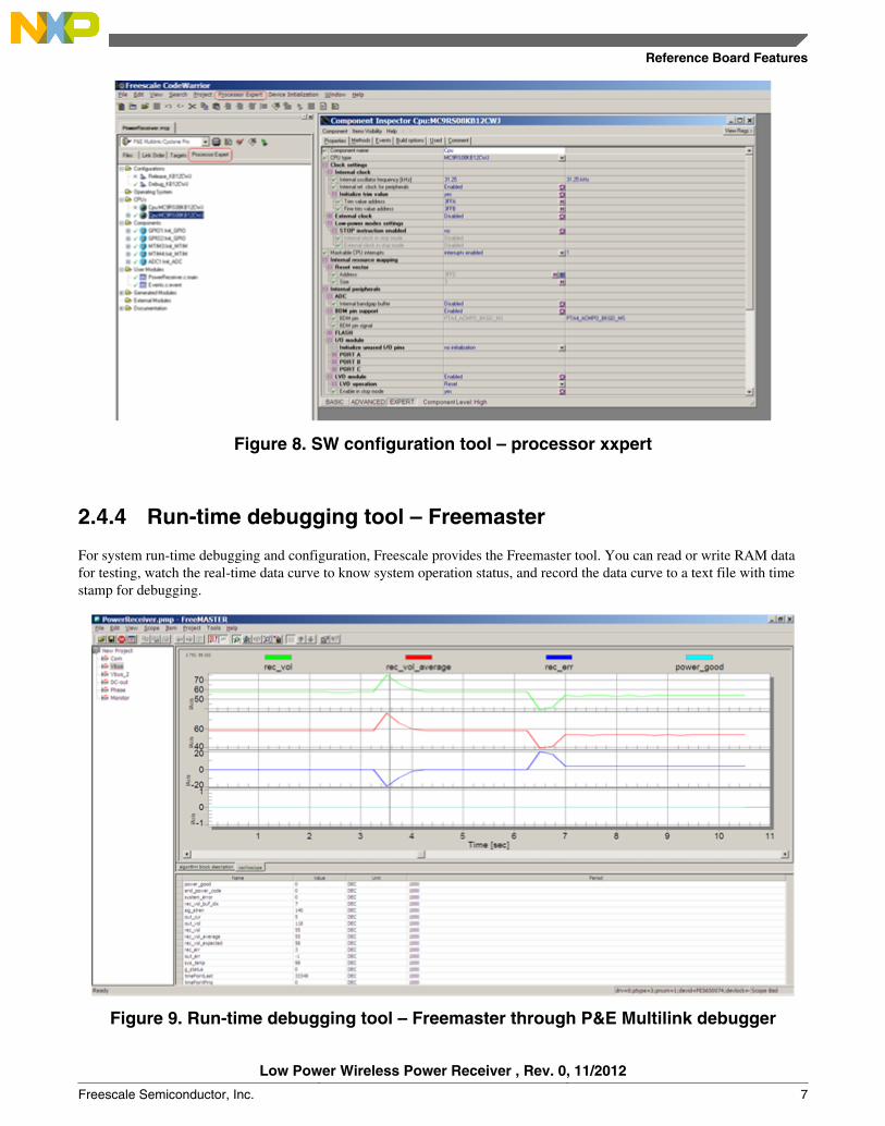
Figure 8. SW configuration tool – processor xxpert
2.4.4 Run-time debugging tool – Freemaster
For system run-time debugging and configuration, Freescale provides the Freemaster tool. You can read or write RAM datafor testing, watch the real-time data curve to know system operation status, and record the data curve to a text file with timestamp for debugging.
Figure 9. Run-time debugging tool – Freemaster through P&E Multilink debugger
Reference Board Features
Low Power Wireless Power Receiver , Rev. 0, 11/2012
Freescale Semiconductor, Inc. 7

Setting -up Freemaster before connecting to the target
Set debugging interface:P&E BDM
Select which P&E BDM debugger connects to the board
Set the binary fileor symbol mapping
Figure 10. Setting Freemaster option
2.5 How to Test
This chapter is about testing.
2.5.1 Test points
Reference Board Features
Low Power Wireless Power Receiver , Rev. 0, 11/2012
8 Freescale Semiconductor, Inc.

Main test points on the receiver board are shown in the figures below.
AC input MCU 3.3 v Vcc DC output
– +
Communication signalRectifier DC output voltage
Figure 11. Test Points on Wireless Power Receiver Board Rev1.2
Reference Board Features
Low Power Wireless Power Receiver , Rev. 0, 11/2012
Freescale Semiconductor, Inc. 9

+ –
Output 5 V / 1A MCU Debugging pins — Reset-BKGD-Vcc_GND
Figure 12. Debugging Pins on the back of the Board
2.5.2 Measurements
Here are several examples that show how to measure and debug the board.
Figure 13 shows the input voltage and communication signal from ping phase to a power transfer setup.
Ch1— Rectifier DC output voltage
Ch2 — Coil AC input voltage
Ch3 — Communication signal
Reference Board Features
Low Power Wireless Power Receiver , Rev. 0, 11/2012
10 Freescale Semiconductor, Inc.

Figure 13. Wireless power receiver ping process
Figure 14 shows the control error signals fed back to the power transmitter when the input voltage changes.
Ch2 —Rectifier DC output voltage
Ch3 —Communication signal
Figure 14. Control error signals response of input voltage change
2.6 References
Get more information from Freescale wireless power charger solution page:
• www.freescale.com/wirelesscharging
RS08KB MCU summary page:• http://www.freescale.com/webapp/sps/site/prod_summary.jsp?code=RS08KB
MCU Debugger: USB BDM Multilink• http://www.freescale.com/webapp/sps/site/prod_summary.jsp?code=USBMULTILINKBDM&fsrch=1• http://www.pemicro.com/universal/index.cfm
SW Developing IDE: Codewarrior Rev 6.3• http://www.freescale.com/webapp/sps/site/prod_summary.jsp?code=CW-MICROCONTROLLERS&tid=CWH
Reference Board Features
Low Power Wireless Power Receiver , Rev. 0, 11/2012
Freescale Semiconductor, Inc. 11

How to Reach Us:
Home Page:www.freescale.com
Web Support:http://www.freescale.com/support
USA/Europe or Locations Not Listed:Freescale SemiconductorTechnical Information Center, EL5162100 East Elliot RoadTempe, Arizona 85284+1-800-521-6274 or +1-480-768-2130www.freescale.com/support
Europe, Middle East, and Africa:Freescale Halbleiter Deutschland GmbHTechnical Information CenterSchatzbogen 781829 Muenchen, Germany+44 1296 380 456 (English)+46 8 52200080 (English)+49 89 92103 559 (German)+33 1 69 35 48 48 (French)www.freescale.com/support
Japan:Freescale Semiconductor Japan Ltd.HeadquartersARCO Tower 15F1-8-1, Shimo-Meguro, Meguro-ku,Tokyo 153-0064Japan0120 191014 or +81 3 5437 [email protected]
Asia/Pacific:Freescale Semiconductor China Ltd.Exchange Building 23FNo. 118 Jianguo RoadChaoyang DistrictBeijing 100022China+86 10 5879 [email protected]
Document Number: LPWPRUGRev. 0, 11/2012
Information in this document is provided solely to enable system and softwareimplementers to use Freescale Semiconductors products. There are no express or impliedcopyright licenses granted hereunder to design or fabricate any integrated circuits orintegrated circuits based on the information in this document.
Freescale Semiconductor reserves the right to make changes without further notice to anyproducts herein. Freescale Semiconductor makes no warranty, representation, orguarantee regarding the suitability of its products for any particular purpose, nor doesFreescale Semiconductor assume any liability arising out of the application or use of anyproduct or circuit, and specifically disclaims any liability, including without limitationconsequential or incidental damages. "Typical" parameters that may be provided inFreescale Semiconductor data sheets and/or specifications can and do vary in differentapplications and actual performance may vary over time. All operating parameters,including "Typicals", must be validated for each customer application by customer'stechnical experts. Freescale Semiconductor does not convey any license under its patentrights nor the rights of others. Freescale Semiconductor products are not designed,intended, or authorized for use as components in systems intended for surgical implantinto the body, or other applications intended to support or sustain life, or for any otherapplication in which failure of the Freescale Semiconductor product could create asituation where personal injury or death may occur. Should Buyer purchase or useFreescale Semiconductor products for any such unintended or unauthorized application,Buyer shall indemnify Freescale Semiconductor and its officers, employees, subsidiaries,affiliates, and distributors harmless against all claims, costs, damages, and expenses, andreasonable attorney fees arising out of, directly or indirectly, any claim of personal injuryor death associated with such unintended or unauthorized use, even if such claims allegesthat Freescale Semiconductor was negligent regarding the design or manufacture ofthe part.
RoHS-compliant and/or Pb-free versions of Freescale products have the functionality andelectrical characteristics as their non-RoHS-complaint and/or non-Pb-free counterparts.For further information, see http://www.freescale.com or contact your Freescalesales representative.
For information on Freescale's Environmental Products program, go tohttp://www.freescale.com/epp.
Freescale™ and the Freescale logo are trademarks of Freescale Semiconductor, Inc.All other product or service names are the property of their respective owners.
© 2012 Freescale Semiconductor, Inc.