Embed Size (px)
Citation preview

Low Power VLSI Circuits and Systems Prof. Ajit Pal
Department of Computer Science and Engineering Indian Institute of Technology, Kharagpur
Lecture No. # 09
MOS Inverters - IV
Hello, and welcome to today’s lecture on MOS inverters driving large capacitive loads.
In the last three lectures, we have discussed various characteristics of MOS inverters,
their configuration, what are the three different ways by which you can realize MOS
inverters, their characteristics voltage transfer characteristics, then your switching
characteristics. And today I shall discuss about how MOS inverters can be used to drive
large capacitive loads efficiently.
(Refer Slide Time: 00:57)
And this is the agenda of today's lecture; after giving a brief introduction, I shall discuss
about various techniques, which are used for driving large capacitive loads; number one
is use of Superbuffers, second is use of Bi CMOS inverters, third is Buffer sizing.
(Refer Slide Time: 01:22)
So, we shall discuss all these techniques one after the other. Coming to the introduction,
there are situations when a large load capacitance such as long buffers off-size capacitive
load or load or IO buffer are to be driven by its gate. See, you are realizing different
circuits by using VLSI technique, but you have to drive some off-chip loads.
(Refer Slide Time: 01:55)
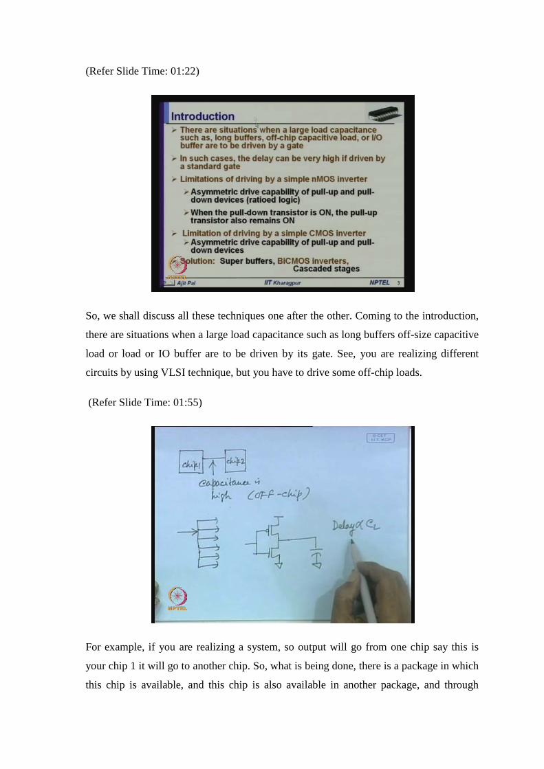
For example, if you are realizing a system, so output will go from one chip say this is
your chip 1 it will go to another chip. So, what is being done, there is a package in which
this chip is available, and this chip is also available in another package, and through
bonding pod connections are taken to the pins, and from the pins connections are taken.
So, whenever you are taking such connections outside the chip the load is very high; that
means, capacitance is very high capacitance is high.
How much high as you know, normally in the based on the present day while I say
circuits the parasitic values of different capacitances, which I have mentioned in my
previous lectures are of the order of femtofarad on the other hand these off-chip loads are
of the order of picofarad. So, you can see there are several orders of magnitude higher
capacive load capacitive loads it has the circuit phases whenever it has to be taken
outside. Similarly, you will require some long buffers you have to drive very at a large
number of outputs whenever it is within the chip for example, the fan-out is very high
you are driving. So, this is coming out from a chip gate and it is going to say large
number of other gates. So, large fan-out here also capacitance is high, but not as high as
the off-chip capacitance this is your off-chip.
So, whenever you are driving such high capacitive loads the delay can be very high if
driven by standard gate what do you really mean by standard gate standard gate means
the gates realized by using minimum dimension. As you know for a particular
technology is lambda is the minimum you know resolution that is permitted by
technology then 2 lambda is the minimum features size. So, normally you can realize a
length is equal to 2 lambda width is equal to L 2 lambda etcetera. So, L by w if it is 2
lambda by 2 lambda for a particular technology then we say that it is of minimum
dimensions. So, whenever you are realizing an inverter using this kind of for minimum
dimension we call it or may be little bigger than that when we have to use little larger I
mean the L by w values may be little different from minimum values then we call it
standard gate.
So and when if the load is very high and as you know this in such cases delay is
proportional to C L in the last lecture, I have derived an expression where it has been
mentioned that delay is proportional to C L. So, whenever this is 3 orders of magnitude
compared to the parasitic capacitances within the chip then the delay can be several
orders of I mean can be very high. So, in such a case what can you do? We have to
develop technique such that the delay can be minimized; obviously, delay cannot be
delay will be there, or objective will be to minimize it to on to how this can be done let
us look at the limitations of the standard gates. First let us consider a simple n MOS

inverter we are starting with n MOS inverter because that super buffer super buffer
which I have mention has been introduced essentially in the context of n MOS inverters.
So, how do you realize a n MOS inverters.
(Refer Slide Time: 06:11)
N MOS inverter the best possible congfiguration as we have seen can be realize by using
a n MOS depression type transistor as pull-up here and this is connected to the source
this is V d d and this is connected to ground and here you apply input voltage, and here
you take the output voltage. So, in such a case as you can see we are using a standard n
MOS inverter where as you know there are 2 problems number one problem is
asymmetric device drive asymmetric drive capability of pull-up and pull-down devices
because of ratioed logic.
As we know that L by w ratio has to be 4 is to 1 minimum and the whenever this is 1 is
to 1; that means, you have to maintain a ratio between the L by w ratio of the pull-up
device by the pull-down device. So, whenever this is a situation there is a asymmetric
behaviour in the switching characteristics and whenever you are charging and
discharging a capacitive load; that means, it has to be charged through this device having
length is equal to 4 into 2 lambda compared to here it is only 2 lambda length is 2
lambda. So; that means resistance of this device is at at least fourth times of that of the
pull-down device as a result the t p low to high is large compared to t p high to low
So, high to low low to high is larger than the high to low. So, high to low it is getting
discharge here. So, the because of the ratioed logic this is one problem. What is the
second problem? Second problem is when the pull-down transistor is on the pull-up
transistor also remains on you see normally, the resistance of this device is small. So, the
discharge time will be shorter, but unfortunately it it has to fight 2 enemies what are the
who are the 2 enemies number one is the current that is being supplied by this pull-up
device because that is that transistor always on. So, that current has to be will also pass
through the pull-down device when the out the capacitor is getting discharge; that means,
this current and also the current that is required to discharge these capacitors. So, this
pull-down device has to sink the current of supplied by the pull-up device and also the
current required to discharge this capacitor and as a consequence whenever this t p high
to low also is affected because of this and it is also not very small and as a consequence
delay is very large. So, question naturally arises is there anyway by which these 2
behaviours these 2 problems number 1 is asymmetric behaviour number 2 is the pull-
down device has to sink the current of the pull-up device when the output is going from
high to low. So, that is where we shall introduce super buffer.
Super buffer will overcome these 2 problems now coming to limitation of driving by a
simple C MOS inverter. So, in case of C MOS inverter fortunately, that asymmetric
behaviour can be overcome to such extent by using devices of proper size we have seen
that. You see this is a C MOS inverter here at least the second problem that does not
arise; that means, when this transistor is on this transistor is off and as a consequence the
pull-down device need not really sink the current supplied by the pull-up device because
pull-up device turns off. So, that is the advantage of C MOS inverter, but unfortunately
what happens whenever this is driving another stage you can see here the capacitance is
quite large compared to n MOS because in case of n MOS this stage will be driving a
only the it will go only to the n MOS transistor the p MOS transistor if it is an inverter.
You can see sorry this will be like this. So, it will go to only the gate. So, gate of the n
MOS transistor as a result the capacitance of this will be much smaller compared to
capacitance that will be faced by a C MOS inverter. So, you can see here here it has to
drive the p MOS transistor and n MOS transistor as you know to to have asymmetric
characteristic the width of for this device has to be 3 by 3 times; that means, W by L
ratio if we write this has to be 3 is to 1 and this will be 1 is to 1. So, that mean the
capacitance that it will face is fourth times that of a n MOS inverter. So, we can see that
C MOS circuits although you know the current drive capability is little larger, but the
capacitance is also larger and as a consequence it has been found that the delay of a n
MOS inverter and a C MOS inverter is comparable; that means, in case of C MOS
inverter you are getting more drive capability, but the capacitance is larger and a
consequence the the C MOS inverter is not really very fast; that means, the n MOS and C
MOS inverters have comparable comparable delay characteristic.
So, question arise naturally arises how can you really minimize the delay in case of a C
MOS inverter? So, for that purpose we shall see one solution have has been provided that
is you know, use of Bi C MOC inverter Bi C MOS. As you know bipolar transistors have
very large current drive capability, but they suffer from lower input impedance on the
other hand C MOS has higher input impedance because input is applied to a gate and
where because of the presence of silicon dioxide you know that input impedance is high
how to get best of both the worlds.
So, high input impedance of n MOS larger driving capability of bipolar devices that is
what is being achieved with the help of Bi C MOS inverters; that means, here you will
see we shall combine bipolar transistors and C MOS devices; that means, C MOS
inverters to realize by C MOS inverters to achieve lower delay. Then finally, another
technique we shall discuss that is your cascaded stages we shall see that instead of using
a single large driver it is more beneficial to use several inverters or drivers of
increasingly larger size to reduce the delay later on we shall discuss about it that is called
the cascadede dipher stages of increasing stage ratio.
(Refer Slide Time: 14:49)
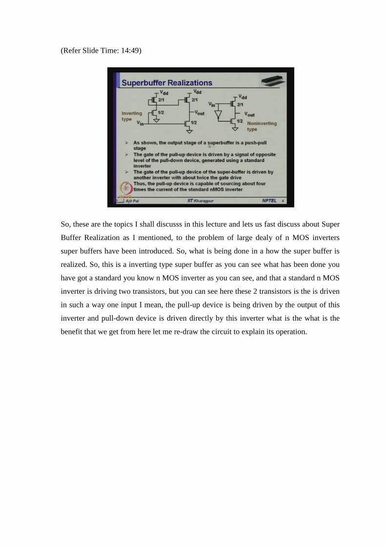
So, these are the topics I shall discusss in this lecture and lets us fast discuss about Super
Buffer Realization as I mentioned, to the problem of large dealy of n MOS inverters
super buffers have been introduced. So, what is being done in a how the super buffer is
realized. So, this is a inverting type super buffer as you can see what has been done you
have got a standard you know n MOS inverter as you can see, and that a standard n MOS
inverter is driving two transistors, but you can see here these 2 transistors is the is driven
in such a way one input I mean, the pull-up device is being driven by the output of this
inverter and pull-down device is driven directly by this inverter what is the what is the
benefit that we get from here let me re-draw the circuit to explain its operation.

(Refer Slide Time: 15:51)
So, as you know this is a standard n MOS inverter. So, what has been done here you
apply the input voltage we have used 2 more transistors. Obvioulsy, one pull-up and
another pull-down, but instead of connecting the gate of this n MOS depression type
transistor this is connected to the output of the first of this first stage of inverter and then
input is applied directly to this. Now let us consider 2 different situation let us assume
here we have applied V d d let us assume we are using this ratio W by L ratio 1 is to 2 2
is to 1 2 is to 1 1 is to 2 W by L ratio are mentioned here. Now in such a case what will
be the how this circuit will operate? Let us assume your input voltage is equal to 0 volt
when the input voltage is 0 volt what will happen this particular input will be 0. So, this
this this transistor.
Let me write down the trsnsistors Q 1 Q 2 this is Q 3 and this is Q 4. So, in this case Q 3
is off what about Q 4? You can see here what is happening the these input is 0 as a
consequence this transistor is off and; obviously, here we shall get large drive to this
transistor; that means, the drive to this transistor is quite large and because here it it will
be very close to V d d of course, it will be V d d only because this transistor will reamin
on throughout as a result we applied it will apply V d d input output to the input of this
particular transistor. As a consequence Q 3 Q 4 is on not only on Q 4 gets large drive
why I am telling large drive why large the reason is normally this gate is connected to
source. So, gate to source voltage is 0, but here you can see in this paticular case it is no
it is not true this is connected to V d d as a consequence this will this the charging time
will be qutie large I mean sorry charging time will be quite small, because this it is
getting large drive and current supply that will come from this n MOS depression type
transistor will be large. Now let us consider V in is equal to V in is equal to V d d in this
case what will happen Q 3 is on what about Q 4 in this case as you can see whenever this
is V d d this is this is on. So, here what will be the output here you will get it will
generate a output which is equal to which will be equal to 0. So, whenever you are
applying a 0 volt here what will happen to this transistor?
This transistor will turn off, because with respect to this this is on this transistor is on.
So, here this transistor will be on and as a consequence what will happen this transistor
will turn off Q 4 will be turn off. So, what is happening now the Q 3 need not really sink
2 currents one coming from the pull-up device another coming from the capacitor. So, as
a consequence this discharge time also will be faster.
That means in this particular gate we can see the gate of pull the pull-up device is driven
by signal of opposite level of the pull-down device generated by standard inverter the
gate of the pull-up device of the super buffer is driven by another inverter with about
twice the gate drive as I have already explained thus the pull-up device is capable of
sourcing about fourth times the current of the standard n MOS inverter. Normally as you
know because of the ratioed logic we get one fourth current, but we can see here because
of this larger drive it will be able to supply large current that we can really explain by we
can really do some computation.
(Refer Slide Time: 20:55)
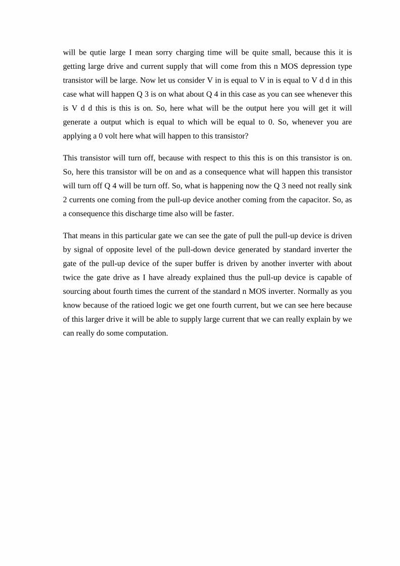
Let us do some computation about the 2 cases one is your Standard inverter another the
other side we shall conside the compute the Super buffer. So, how the current of these 2
are different. So, first of all as we know I d s saturation that is equal to as you know beta
pull-up by 2 V g s minus V t d e p where V d e p is equal to roughly about minus 3 volt.
You know this this p MOS transistor the dipression type transistor will turn off and you
apply minus 3 volt that is why this is the volt. In such a case if you suupply if you
substitute the values we shall be getting this is equal to beta p u by 2 into this is this
voltage is 0 now. When the input voltage is 0 so, 0 plus 3 square. So, that is equal to the
roughly 4 point; that means, 3 into 3 9 by 24.5 beta p u. So, this is the current that is
being supplied by the by the transistor when they were, it is in saturation what about the
current whenever it is in the linear region.
Then this equal to beta p u by 2 beta p u by in this case it will be V g s minus V i v v plus
d p minus V d s square by 2. So, this is the expression for linear region. In this case if we
substitute various values say V g s V d s is equal to of course, here there will be V g s V
d s another turn will be there as we have taken the V d s inside. So, if we substitute
various value we find this is equal to roughly 4.38 beta p u; that means,. So, in case of
standard inverter the current drive is like this; that means, partially this partcular inverter
when it is charging this capacitor part of the time it will be in saturation part of the time
it will be linear mode I mean, sorry this particular transistor part time it will be in
saturation part of the time in the linear mode as a consequence the average current if you
take up which will be equal to if you take the average this will be roughly equal to 4.4
beta p u. This is the average current that will be supplied for pulling the device on; that
means, the source current source current for a simple inverter.
Now let us consider in case of super buffer. So, in case of super buffer, I d s whenever
you are applying 5 volt. So, that time what is the drive because it is getting the drive of
five volt whenever you are charging this capacitor. So, that time the it will be voltage
will be beta p u by 2 into 2 into 5 plus 3 into 5 minus 5 square. It is in the linear region
that is why this is the expression and this we get 27.5 beta p u, and whenever I d s is
equal to 2 volt; that means, we are assuming that this output is changing. So, initial it
was 5 then it will come down to 2 then we shall take the average. So, when this is when
the output volt is 2 volt that time beta pull-up by 2 again 2 into 2.5 plus 3 sorry, not 2
volt I have taken 2.5 at the middle point and 2 5 into 2.5 minus 2.5 square. So, this if we
calculate it will be equal to 10.62 beta pull-up.
So, if we take the average of the two we will be getting 27.5 plus 10.62 by 2. So, I d s
average will be equal to 27.5 plus 10.62 by 2 beta p u. So, this is roughly equal to 19.06
beta p u as I was telling it will be about fourth times. So, 4.4 that is the standard inverter
19.06 for the super buffer. So, we find that driving capability is quite large and as a result
that asymmetric characteristic no longer present and of course, I am not there is no
problem about discharging, because the resistance is length is small as you can see one
fourth and as a consequence the discharge time has not been considered, but it is more or
less comparable for both the cases, but in this case also it is getting discharge by the
same type of same transistor of the same size here also the same thing. So, there is no
difference. So, for as a discharge time is concerned, but asymmetry was present only for
the charging time and that is being alleviated with the help of super buffer. So, this is
roughly equal to 4.3 times of a standard inverter.
So, this is the super buffer. Now let us consider non-inverting type this is the inverting
type because whatever input we apply you get the inverted output here, but in this
particular case the connection is done in little different way only instead of applying this
input to this pull-down device the input is applied to the pull-up device and output of the
inverter is applied to the input of the pull-down device. So, this converts the inverter into
a non-inverting types super buffer and; obviously, the characteristics will be similar to
what I have alredy discussed. So, you find that the super buffer can be realized both
inverting type and non-inverting type and that offer comes some of the limitation of
standard n MOS inverter.
(Refer Slide Time: 28:25)
So, this is the use of super buffer now we shall come to the second topic that is your bi-C
MOS inverter. As I mentioned the C MOS is although it is good, but its delay
characteristic is not very good, I have already mentioned that because of large
capacitances.
(Refer Slide Time: 28:28)
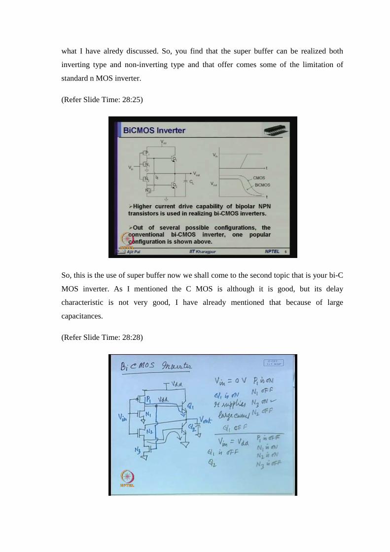
So, this can be modified to realize a bi-C MOS inverter by adding both bipolar and
bipolar devices and C MOS devices how it can be done? So, let me draw a BiC MOS
inverter actually, you can have different types of realizations of BiC MOS inverter, but I
shall I m considering the simplest and the most standard one. So, this is the diagram of
that you have got the basic inverter is here.
This is connected to the V d d now this output is it is driven is driving a bipolar
transistor. So, you can see this is a N P N type transistor V d d. So, instead of driving
using a MOS transistor a bipolar transistor is used of course, you will have a kind of
push-pull realization push-pull realization means you will be having 2 devices. So, when
one is on another one will be off. So, here also you will require 2 transistors. So, here are
the 2 transisitors bipolar transistors, but you can see both are N P N type. And then this is
connected to ground what is being done we have to realize in such a way, that when this
is on this is off and when this is off this is on to do that we shall be using another 2
additional transistors. This is connected to the base of this transistor and this is connected
to the output and this one we have got another transistor here, n MOS transistor this is
connected to this particular line. So, we have got how many devices. So, you have got 2
bipolar transistors and 4 MOS transistors and these are say this is your P 1 P type
transistor this is N 1 n MOS transistor this is N 2 this is N 3 and here you are applying
input you are taking output from here this is your V out.
Now, let me explain the operation of this Bi C MOS inverter. How it really works? Let
us assume V in is equal to V in is equal to 0 volt. So, when V in is equal to 0, as you
know this P 1 will be on P 1 is on N 1 off I shall discuss about N 3 and N 4 little later,
and what about this makes whenever P 1 is on wat is what is the voltage here you will
get V d d. So, this will make N 3 on what about this transistor since V in is equal to 0 N
2 will be off. So, this is these are the states of these fourth transistor.
Now, about these 2 transistors since P 1 is on, the drain current of this transistor is will
pass through this Q 1 transistor and as a consequence you can see here you will have
large base current. So, this will be the base current the the the drained current of P 1 is
the base current of Q 2 and; obviously, Q 2 if it is having the beta of 100, the current that
will be able yo supply is 100 times that of the drained current of the p MOS transistors.
So, it will be able to supply very large current.
So, Q 1 is on and it can drive it supplies large current; that means, the pull-up time will
be quite fast. Now let us see whether this transistor is off whenever this is on or not
otherwise you know this transistor has to fight with the this transistor to dry when
driving this, because some of the current that it will supply pass through the will be by
passed by these transistor. So, whether this is prevented or not let us see what happens in
the particular case in this particular case as you know this N 3 is on as you have seen. So,
this N 3 actually clamps the base of these Q 2 transistors; that means, the Q 3 is acting as
a kind of clamping device it it actually the base of the Q 2 transistor is clamped to almost
0 volt. So, what will happen in that case Q 2 will be off as you know a this is a silicon
transistor by pull-up transistor by pull-up transistor to make it on you will require point
six volt. So, whenever the voltage here is 0, base 2 a meter then this will be off. So, this
makes Q 1 off as a consequence the Q 1 need not fight with Q 2 while driving this
capacitor so; that means, the there will be no current no current will pass through Q 2
when Q 1 is on
Now, let us consider this is one situation what about when V in is equal to V d d when V
in is equl to V d d then what will happen let me write down the state of different
transistor P 1 is off P one will be off because this input is V d d N 1 is on N 2 what about
N 2? N 2 also will be on N 2 will be on and what about N 3? N 3 is off. So, now, how
these how the state of this 4 transistor effects the bipolar devices let us see. So, whenever
P 1 is off this particular device does not really get any drive it does not really get any
drive, but what happens at that time you know this transistor this N 1 transistor the
transistor N 1 was is now on. So, what it will do?
It will act as clamping device N 1 that means, Q 1 is off. So, Q 1 will be off because this
voltage will be pulled to 0 volt it will by making this transistor off what about Q 1 Q 2, Q
Q 2 as you can see this transistor is on, the drained current of N 2 will pass through base
of this transistor Q 2; that means, the current of N 2 will now be will now supply the best
current of Q 2 as a result the current drive the current drive for this Q 2 will be large; that
means, it will be able to discharge this capacitor with a large current and as a
consequence you know that this we have seen the role of N 3 essentially, to clamp the
this output, role of N 2 supplying current when this transistor is on role of N 1 and N 2
you have seen. So, these 4 transistors actually ensures the push-pull behaviour of Q 1and
Q 2. So, by ensuring that we are able to not only drive large capacitive load because the
current that can be supplied by the bipolar transistors Q 1 and Q 2 is very large and you
know when Q 1 is on it is ensure that Q 2 is off and so on.
(Refer Slide Time: 38:29)
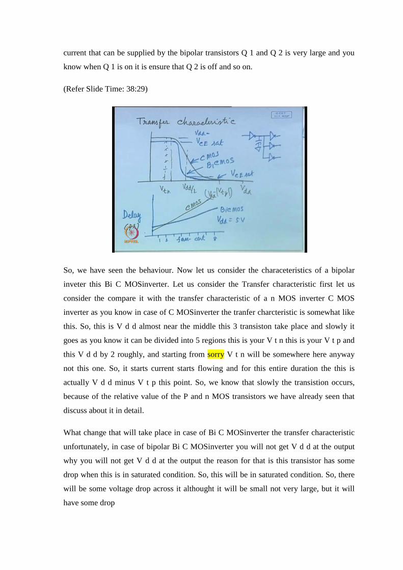
So, we have seen the behaviour. Now let us consider the characeteristics of a bipolar
inveter this Bi C MOSinverter. Let us consider the Transfer characteristic first let us
consider the compare it with the transfer characteristic of a n MOS inverter C MOS
inverter as you know in case of C MOSinverter the tranfer charcteristic is somewhat like
this. So, this is V d d almost near the middle this 3 transiston take place and slowly it
goes as you know it can be divided into 5 regions this is your V t n this is your V t p and
this V d d by 2 roughly, and starting from sorry V t n will be somewhere here anyway
not this one. So, it starts current starts flowing and for this entire duration the this is
actually V d d minus V t p this point. So, we know that slowly the transistion occurs,
because of the relative value of the P and n MOS transistors we have already seen that
discuss about it in detail.
What change that will take place in case of Bi C MOSinverter the transfer characteristic
unfortunately, in case of bipolar Bi C MOSinverter you will not get V d d at the output
why you will not get V d d at the output the reason for that is this transistor has some
drop when this is in saturated condition. So, this will be in saturated condition. So, there
will be some voltage drop across it althought it will be small not very large, but it will
have some drop
So, what will happen the here the transition occur very fast not like this one slow and
then it remain it will be somewhat like this; that means, the transition occur very fast, but
it will not go to 0 then why it will not go to 0 again there will be a voltage drop across
this transistor V C E that is not 0 in case of you know bipolar transistors and as a
consequence you are getting this V C E sat V d d minus V C E sat here this this part.
Similarly, here you are getting V C E sat of the pull-down device. So, we find that this
there is some voltage drops small hold is there, but transition will be very fast because of
large switching. So, this the transfer characteristic of a this is for C MOS and this is for
Bi C MOS. Now let us study another behaviour. How the inverters behave whenever you
change the faning whenever you change the change the fan-outs not fan in fan-out what
is fan-out fan-out is you know say here is an inverter inverter will be driving several
loads it can if it drives only one gate then fan-out is 1, if it drives 2 gate then fan-out is
two if it drives 3 gate then fan-out is 3 and so on. That means, as the fan-out increases of
this particular gate then the output capacitance also increses because the drive that you
know the capacitance value that it will face as load capacitance will keep on increasing.
So, you can do an experiment you can study the switching charcteristics for different
values of you know load capacitance or different value of fan-out by adding one gate
adding another gate adding another gate then you can measure the delay. So, on this we
shall be measuring the delay and here it is fan-out say it is increasing from 1 2 3 4 5 6 7 8
and so on. So, if fan-out is increasing 1 2 3 4 5 6 7 8 let us assume. And how how the
dealy will increase let us assume this is the delay characteristics of a C MOS inverter.
So, this delay will be in pico-second in what way it will be different in case of BiC MOS
inverter. In case of Bi C MOS inverter it has been found that delay characteristic will be
somewhat like this; that means, delay will definitely increase, but for C MOS inverter it
will increase at the faster rate compared to standard C MOS inverter.
This is for Bi C MOS and this for C MOS standard CMOS. Now you may be wandering
initially why delay is more for Bi C MOS compared to standard CMOS, initially for fan-
out of one or 2 delay is larger for Bi C MOS compared to standard C MOS why is it. So,
the reason for that is you can see Bi C MOS inverter is a little complex. So, you know
this this paticular inverter is driving this transistor. So, the path delay will be little larger
whenever the load is small compared to if you take the output from here; that means,
compared to a simple inverter for a Bi C MOS inverter delay will be larger because you
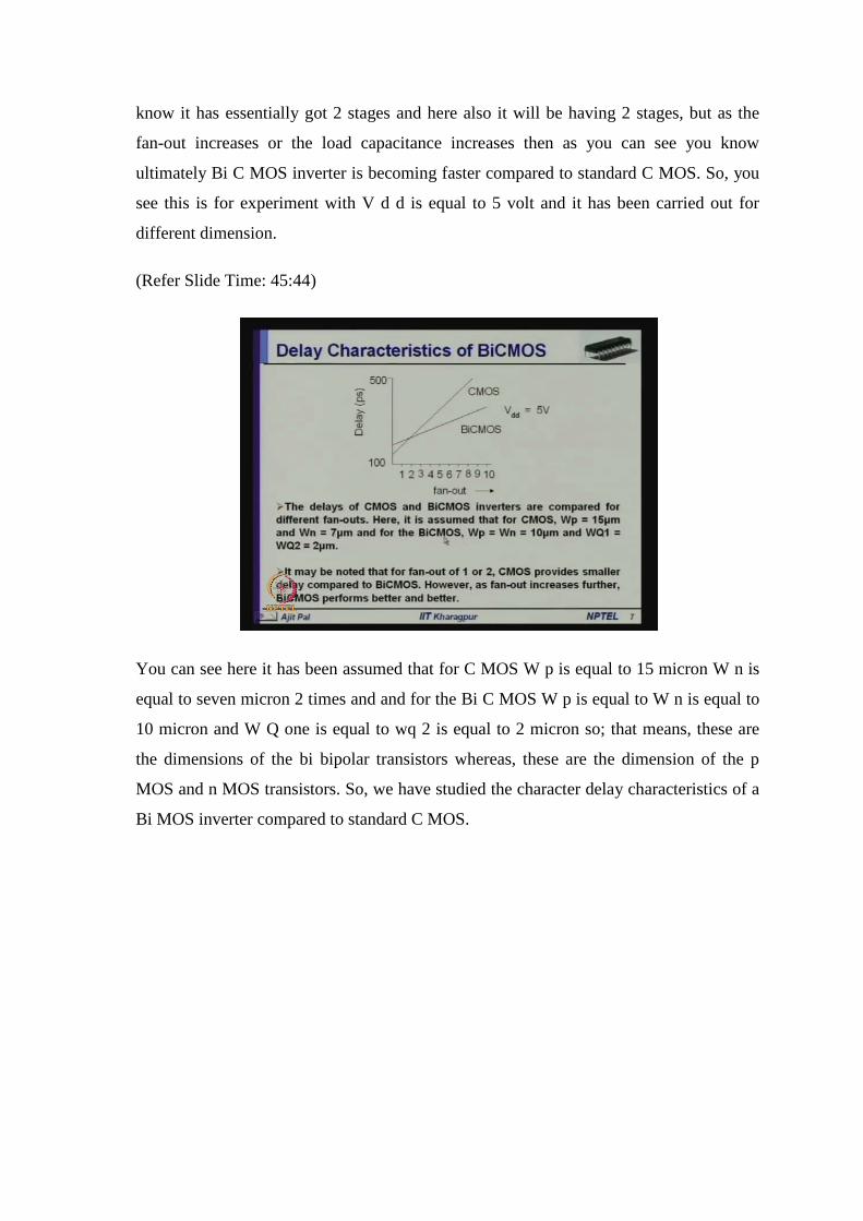
know it has essentially got 2 stages and here also it will be having 2 stages, but as the
fan-out increases or the load capacitance increases then as you can see you know
ultimately Bi C MOS inverter is becoming faster compared to standard C MOS. So, you
see this is for experiment with V d d is equal to 5 volt and it has been carried out for
different dimension.
(Refer Slide Time: 45:44)
You can see here it has been assumed that for C MOS W p is equal to 15 micron W n is
equal to seven micron 2 times and and for the Bi C MOS W p is equal to W n is equal to
10 micron and W Q one is equal to wq 2 is equal to 2 micron so; that means, these are
the dimensions of the bi bipolar transistors whereas, these are the dimension of the p
MOS and n MOS transistors. So, we have studied the character delay characteristics of a
Bi MOS inverter compared to standard C MOS.
(Refer Slide Time: 46:25)
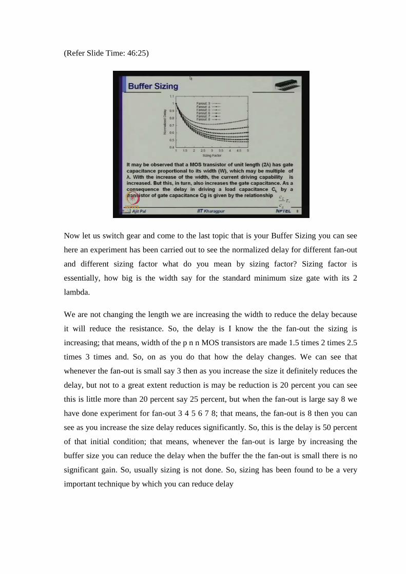
Now let us switch gear and come to the last topic that is your Buffer Sizing you can see
here an experiment has been carried out to see the normalized delay for different fan-out
and different sizing factor what do you mean by sizing factor? Sizing factor is
essentially, how big is the width say for the standard minimum size gate with its 2
lambda.
We are not changing the length we are increasing the width to reduce the delay because
it will reduce the resistance. So, the delay is I know the the fan-out the sizing is
increasing; that means, width of the p n n MOS transistors are made 1.5 times 2 times 2.5
times 3 times and. So, on as you do that how the delay changes. We can see that
whenever the fan-out is small say 3 then as you increase the size it definitely reduces the
delay, but not to a great extent reduction is may be reduction is 20 percent you can see
this is little more than 20 percent say 25 percent, but when the fan-out is large say 8 we
have done experiment for fan-out 3 4 5 6 7 8; that means, the fan-out is 8 then you can
see as you increase the size delay reduces significantly. So, this is the delay is 50 percent
of that initial condition; that means, whenever the fan-out is large by increasing the
buffer size you can reduce the delay when the buffer the the fan-out is small there is no
significant gain. So, usually sizing is not done. So, sizing has been found to be a very
important technique by which you can reduce delay

(Refer Slide Time: 49:36)
Obviously, in this world nothing is free the area increases. So, you are trading area for
smaller delay. You are paying the price in terms of area as you are increasing the size the
dimension of the devices will increase that will increase the area. So, at the cost of the
area you are reducing the dealy. So, in a present day high performance circuits delay may
be more important than area because of the reduced you know increasingly reduced
dimensions you have abundant space for fabricating millions of transistors, but we want
higher performance. So, what can be done you can trade area for delay that is a reason
why sizing is very important technique for reduce the delay.
(Refer Slide Time: 50:11)

Now let us now consider a situation in which a large capacitive load like output pad is to
be driven by a MOS gate and as I have already mentioned typical value can be of the
order of hundred picofarads. So, it is quite large. So, if such a load is driven by MOS
gate minimum dimension of minimum dimension, then delay can be 10 to the power 3
tau.
So, let me first introduce this term tau what is tau actually is called the unit of delay
whenever you are driving an inverter of minimum dimension, another inverter of
minimum dimension then whatever is the delay because here you can see the resistance
is decided by the W by L of this and capacitance is also decided by the W by L. So,
assuming that there are of minimum dimensions then whatever is the delay for driving a
gate of unit dimension minimum dimension by gate of another inverter of minimum size
whatever is the delay we call it tau. With respect to this tau we shall compare the delay
whenever say lets assume here we have to drive a large capacitive load say this
capacitance is 1000 times that of C g. C g the gate capacitance together of this. So,
compare to this this is 1000 times. So, what will be the delay? You see the capacitance is
larger resistance is same as this. So, as a it can be proved that the delay will be equal to
1000 tau.
Now, you may say now I shall what I shall do I shall put a an inverter and then a large
inverter with width is equal to 1000 times that of the standard minimum gate. So, in this
case what will be the delay again this is 1000 C g what will be the delay for this. So, here
here it will be facing a capacitance of 1000 C g again, because you know here you have
put the dimension has been made 1000 times larger. So, delay of this gate will be again
1000 tau may be, but the dealy of this gate will now reduce it will become tau because
resistance is now very small and you are driving the capacitance because the realtive
value of resistance and capacitance is dependent so; that means, the total dealy will be
thousand one tau in this particular case.
Now, let us consider a situation where instead of doing this, let us increasingly change
the size. So, here it is one is to one inverter ratio this is 10 is to one here it is 100 is to
one; that means, with respect to minimum dimension what has been done here this is this
inverter of minimum size this is the size of this is 10 times that of the minimum size and
the size of this is 100 times to that of the minimum size. So, what will be the delay total
delay in this particular case. So, here how much capacitance is faced? 10 C g here how
much capacitance it will face? 100 C g and here as we have seen we have put a
capacitance of 1000 C g as the original. So, what will be the delay of this? 10 tau. what
will be the delay of this? What will be the dealay of this? So, you find it is 30 tau
compared to 1000 tau in this particular case we are finding thousand one tau in this case
we are getting only 30 tau. This is a significant reduction. So, question is by having a
cascaded stage or stages of inverter we can reduce the delay significantly question is here
the the question is how many stages and what will be the increasing stage ratio you have
to optimize it I have elastated this with the help of stage ratio obtained, but is the is this
delay minimum.?
Can we achieve still lower delay? That can be done uh what what has been done we have
decided to get optimal stage ratio.
(Refer Slide Time: 54:55)
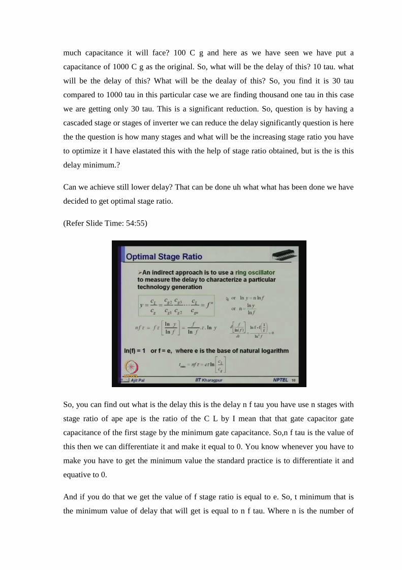
So, you can find out what is the delay this is the delay n f tau you have use n stages with
stage ratio of ape ape is the ratio of the C L by I mean that that gate capacitor gate
capacitance of the first stage by the minimum gate capacitance. So,n f tau is the value of
this then we can differentiate it and make it equal to 0. You know whenever you have to
make you have to get the minimum value the standard practice is to differentiate it and
equative to 0.
And if you do that we get the value of f stage ratio is equal to e. So, t minimum that is
the minimum value of delay that will get is equal to n f tau. Where n is the number of
stages f is the stage ratio and tau is the unit delay as you have seen. So, it is e tau l n C L
by C g C L by C g is the C L is the load capacitance and C g is the gate capacitance. So,
with this we this is the minimum delay we are getting. Unfortunately, this value of f is
equal to e is quite small it is is equal to 2 you know 2.7. So, with this value of stage ratio
you will require large number of stages what is the effect of this large number of stages
effect of large number of stages effect of large number of stage
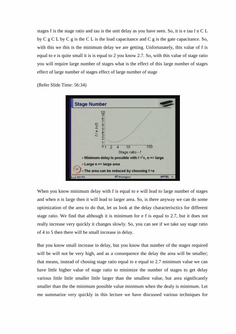
(Refer Slide Time: 56:34)
When you know minimum delay with f is equal to e will lead to large number of stages
and when n is large then it will lead to larger area. So, is there anyway we can do some
optimization of the area to do that, let us look at the delay characterisctics for different
stage ratio. We find that although it is minimum for e f is equal to 2.7, but it does not
really increase very quickly it changes slowly. So, you can see if we take say stage ratio
of 4 to 5 then there will be small increase in delay.
But you know small increase in delay, but you know that number of the stages required
will be will not be very high, and as a consequence the delay the area will be smaller;
that means, instead of chosing stage ratio equal to e equal to 2.7 minimum value we can
have little higher value of stage ratio to minimize the number of stages to get delay
various little little smaller little larger than the smallest value, but area significantly
smaller than the the minimum possible value minimum when the dealy is minimum. Let
me summarize very quickly in this lecture we have discussed various techniques for

driving large capacitive load use of super buffer use of Bi C MOS inverter and finally,
you know use of cascading of a number of stages amd also by using buffer sizing. Thank
you very much this is the last lecture on in MOS inverters in the next lecture we shall
discuss about complex combinational circuits. Thank you.