Embed Size (px)
DESCRIPTION
LPVLSI
Citation preview

1
Low Power System DesignLow Power System Design
Module 4 (3 hours):Low-Voltage Low-Power VLSI CMOS Circuit Design
Jan. 2007
Naehyuck ChangEECS/CSESeoul National University

2
ContentsContents
Lowering VDD (voltage islands, dynamic voltage scaling)Cooling and/or refrigerationSOI technologyDual Vt designBody bias control (static and/or adaptive)Input vector control during sleep mode

3
Cooling and/or RefrigerationCooling and/or Refrigeration

4
Cooling and/or RefrigerationCooling and/or Refrigeration
Increasing temperatureReduces mobilityReduces Vt
ION decreases with temperatureIOFF increases with temperature
Vgs
dsI
increasingtemperature

5
Silicon on Insulator (SOI)Silicon on Insulator (SOI)
Silicon on insulator technology (SOI) refers to the use of a layered silicon-insulator-silicon substrate in place of conventional silicon substrates in semiconductor manufacturing, especially microelectronics

6
Silicon on Insulator (SOI)Silicon on Insulator (SOI)
Silicon-On-Insulator (SOI) is a new type of starting material for the chip-making process, that replaces bulk silicon wafers (approximately 0.75 mm thick) with wafers which have three layers
A thin surface layer of silicon (from a few hundred Angstrom to several microns thick) where the transistors are formedThe insulating layer, usually made of silicon dioxide is referred to as the "buried oxide" or "BOX", and is usually a few thousand Angstroms thick An underlying layer of insulating material on a support or "handle" bulk silicon wafer

7
Silicon on Insulator (SOI)Silicon on Insulator (SOI)
SOI-based devices differ from conventional silicon-built devices in that the silicon junction is above an electrical insulator, typically silicon dioxide or (less commonly) sapphireThe precise thickness of the insulating layer and topmost silicon layer also vary widely with application

8
MOS Transistor on SOIMOS Transistor on SOI
On an SOI waferThe smaller volume of silicon that is depleted during switching of an SOI transistor increases the speed of signal processing and allows operation at lower drive voltages

9
CMOS Inverter on SOICMOS Inverter on SOI
On a bulk silicon wafer, the transistors are formed in a pair of doped "wells"On an SOI wafer, the transistors are formed directly in the thin silicon layer insulated by the buried oxide (or "BOX") – immune to "latch-up" problems The smaller size of the SOI inverter *sketched with the same gate size
(critical dimensions)

10
Technical Advantages of SOITechnical Advantages of SOI
A 20% to 50% increase in switching speedThe ability to operate at lower voltages
Lower Leakage CurrentLower Supply Voltage
Good high-temperature performanceReducing need for error correction operations in high-speed servers and memory arrays operating in environments prone to cosmic ray particle showersIncreased circuit packing density
Increasing chip yield and die count per wafer

11
Faster Switch SpeedFaster Switch Speed
Area between the impurities added to a chip’s silicon and the silicon substrate itself creates “Junction Capacitance”In SOI “junction capacitance” is eliminated for introducing a thin layer of Insulator or Oxide layer
Si
Impurities
A lot of capacitance here (i.e. slow)
Si
No capacitance here (i.e. fast)
Impurities
BOX

12
Lower Leakage CurrentLower Leakage Current
SOI completely isolates the transistor from its neighboring transistors and other circuit components

13
Lower Supply VoltageLower Supply Voltage
SOI circuits can operate at low voltage with the same performance as a bulk technology at high voltage

14
High-temperature PerformanceHigh-temperature Performance
At high temperature SOI transistors have much lower leakage currents than bulk MOSFETs.

15
ApplicationApplication
SOI have a tremendous impact on applications where low power is needed, such as portable and wireless applications
SOI layer thickness for various applications is shown

16
State of The ArtState of The Art
sSOI – ”strained SOI”Strained Si on top of SiGeHigher mobility gives larger drive current in MOS-channelsAlready being used
SOD – ”Si-On-Diamond”Diamond has larger heat conductionBetter heat dissipation through substrate will be increasingly importantSOD might never by used for IC-production, but very cool

17
Use in the Microelectronics IndustryUse in the Microelectronics Industry
Examples of microprocessors built on SOI technology include
AMD's 130 nm and 90 nm Opteron microprocessorsthe 90 nm IBM-based processors used in the Xbox 360 and PlayStation 3
Competitive offerings from Intel, however, such as the 65 nm Core 2 and Core 2 Duo microprocessors, are built on conventional pure silicon substrates.

18
ReferencesReferences
T.Ogawa, “At long last, SOI wafer market on the move,” Solid State Technology, pp.62-65 ,2001.2.S.Billat et al., “Convection-based micromachined inclinometer using SOI technology,” Proc. IEEE-MEMS’01, pp.159-161 ,2001.1.A.Kamgar et al., “Isolation’s path to SOI technology,” Solid State Technology, pp.109-118 ,1999.10.J.Colinge, “Silicon-on-insulator technology: past achievements and future prospects,” MRS Bulletin, vol.23, no.2, pp.16-19 ,1998.12.M.Bruel, “The history, physics, and applications of the Smart-Cut process,”MRS Bulletin, vol.23, no.2, pp.35-39 ,1998.12.http://www.amdboard.comhttp://www.ibis.comhttp://www.semiconductors.philips.comhttp://www.sigen.comhttp://www.soitec.comhttp://www-3.ibm.com/chips/bluelogic/showcase/soihttp://www.wikipedia.org

19
Leakage Reduction OverviewLeakage Reduction Overview
Vdd
High Vt
High Vt
Low V t
Logic
0 1 1 0 1 0
Source: [ Johnson, et al. , DAC99]

20
Dual Vt Circuit OptimizationDual Vt Circuit Optimization
Transistor is assigned either a high or low Vt
Low-Vt transistorReduced delayIncreased leakage
Speed critical path: low-Vt
Rest: high-Vt
Low-Vt; 0.8V High-Vt; 0.8V Low-Vt; 1.2V High-Vt; 1.2V
Leakage (norm) 1 0.050 1 0.049
Delay (norm) 1 1.36 1 1.30

21
Dual Vt Circuit OptimizationDual Vt Circuit Optimization
ObjectiveFind an implementation between the two extremes of all low Vt, all high Vt, trading off leakage power for delayDelay constraint must be met

22
Dual Vt ExampleDual Vt Example
Dual Vt assignment approachTransistor on critical path: low Vt
Non-critical transistor: high Vt
0
0.2
0.4
0.6
0.8
1
All Low Vt Dual Vt
Nor
mal
ized
Lea
kage
cur
rent (Leakage Reduction)
(1x)
(~2x)

23
Vt Assignment ApproachVt Assignment Approach
Greedy approach: backward traversal of circuitSelect high Vt gate in critical pathSet gate to low Vt
Re-compute critical paths0 1 2 3 4 5 6

24
Vt Assignment GranularityVt Assignment Granularity
Vt assignment can be at different level of granularityGate based assignmentPull up network / Pull down network based assignment
Single Vt in P pull up or N pull down trees
Stack based assignmentSingle Vt in series connected transistors
Individually assignment within transistor stacksPossible area penalty
Design rule constraint for different Vt assignment

25
Example of Different Vt Assignment GranularityExample of Different Vt Assignment Granularity
Gatebased
PU/PDbased
Stackbased

26
MaxFlow Formulation of Vt AssignmentMaxFlow Formulation of Vt Assignment
Formulated as a MaxFlow problemFind a Maximal Weighted SubsetUse cuts based on topological levelFind Maximum Weighted Level Cut, over all levels of the graph
a
b
c
d
e
f
g
h
i
j
k
0
0
0
3
2
5 0
10
0
level i-1 level i level i+1
0
0
0
0
00

27
Vt Assignment IssuesVt Assignment Issues
Resizing necessary after Vt assignment to improve obtained trade-off
Transistors changed to low Vt become oversizedInput capacitance increases with low Vt assignment
Path delay distribution of a circuit before and after size optimization

28
Simultaneous Vt and Sizing ApproachSimultaneous Vt and Sizing Approach
Determine the size (width) and threshold voltage for each transistor
AreaPerformanceLeakage current
Both the performance of the circuit and its leakage vary non-linearly with device widths and their Vt
The width domain is continuous while the Vt domain is discrete heuristic approach

29
Simultaneous Vt and Sizing ApproachSimultaneous Vt and Sizing Approach
Example: Sirichotiyakul, et al., DAC99

30
Sensitivity Based Vt SelectionSensitivity Based Vt Selection
In each iteration, pick a transistor with the best trade-off between leakage and delay, weighted by its path slack
( )( ) ,( )
1( ) ( )min( )
where k small negative number
sub
arcs
I TCost T whereD T
D T d Tk slacks slack
α
αα
∆=
∆
∆ = ∆ ×+ −
=
∑
Delay change on timing arc α when transistor T is changed to low Vt (∆dα (T) )

31
Vt and Size Assignment through Lagrangian RelaxationVt and Size Assignment through Lagrangian Relaxation
Example: Karnik, et al., DAC02

32
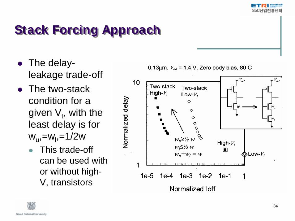
Stack Forcing ApproachStack Forcing Approach
Leakage current difference between a single off device and a stack of two off devices.
As illustrated by the energy band diagram, the barrier height is modulated to be higher for the two-stack due to smaller drain-to-source voltage resulting in reduced leakage

33
Stack Forcing ApproachStack Forcing Approach
Load line analysis showing the leakage reduction in a two-stack
34
Stack Forcing ApproachStack Forcing Approach
The delay-leakage trade-off The two-stack condition for a given Vt, with the least delay is for wu,=wl,=1/2w
This trade-off can be used with or without high-V, transistors

35
Combining Vt and Input State AssignmentCombining Vt and Input State Assignment
Given a known input state in standby mode, only “OFF”transistors set to high Vt
All other transistors are kept at low Vt
0
0.2
0.4
0.6
0.8
1
All Low Vt Dual Vt Randomstate
Nor
mal
ized
Lea
kage
cur
rent
(Leakage Reduction)(1x)
(~2x)
(~7.8x)

36
Combining Vt and Input State AssignmentCombining Vt and Input State Assignment
Optimal input state with Vt assignmentIncreased reduction of leakage current
0
0.2
0.4
0.6
0.8
1
All Low Vt Dual Vt Randomstate
Optimalstate
Nor
mal
ized
Lea
kage
cur
rent (Leakage Reduction)
(1x)
(~2x)
(~7.8x)(~9.7x)

37
Mixed-Vt CMOS DesignMixed-Vt CMOS Design
Mixed Vt (MVT) CMOS design techniqueTransistor-level dual Vt design techniqueTransistors within a gate can have different Vt
Use multiple types of transistors within each gateMVT1: Same threshold voltage for all transistors in N or P networksMVT2: Same threshold voltage only for all transistors of a series stackNo limitation (possible in some processes)

38
MVT CMOS Design AlgorithmMVT CMOS Design Algorithm
Assume all low Vt transistorsFor each transistor of each gate,
Find the increase in the gate delay if high Vt is used (Δtd)Find the decrease in the gate leakage if high Vt is used (Δleak)
Calculate:
Higher value means more leakage can be saved using one unit of slackThe transistors are processed based on their priority (i) valuesAfter modifying each transistor, the slack values have to be recalculated

39
MVT Design ResultsMVT Design Results

40
ReferencesReferences
[Blaauw, et al.] “Emerging power management tools for processor design,” ISLPED 1998, pp.143-148[Halter and Najm] “A gate-level leakage power reduction method for ultra-low-power CMOS circuits,” CICC 1997, pp.475-478[Hamzaoglu, et al.] “Circuit-level techniques to control gate leakage for sub-100 nm CMOS,” ISLPED 2002, pp.60-63[Johnson, et al.] “Models and algorithms for bounds on leakage in CMOS circuits,” TCAD, June 1999, pp.714-725[Lee, et al.] “Static leakage reduction through simultaneous threshold voltage and state assignment,” DAC 2003, pp.191-194[Sundararajan, et al.] “Low power synthesis of dual threshold voltage CMOS VLSI circuits,” ISLPED 1999, pp.139-144[Wang, et al.] “Static power optimization of deep submicron CMOS circuits for dual Vt technology,” ICCAD 1998, pp.490-496[Wei, et al.] “Design and optimization of low voltage high performance dual threshold CMOS circuits,” DAC 1998, pp.489-494

41
ReferencesReferences
[Ye, et al.] “A new technique for standby leakage reduction in high-performance circuits,” Symp. VLSI Circuits 1998, pp.40-41[Kawaguchi, et al.] “A CMOS scheme for 0.5 V supply voltage with pico-ampere standby current,” ISSCC 1998, pp.192-193, 436[Sirichotiyakul, et al.] “Stand-by power minimization through simultaneous threshold voltage selection and circuit sizing,” DAC 1999, pp.436-441[Karnik, et al.] “Total power optimization by simultaneous dual-Vtallocation and device sizing in high performance microprocessors,”DAC 2002, pp. 486-491[Ketkar and Sapatnekar] “Standby power optimization via transistor sizing and dual threshold voltage assignment,” ICCAD 2002, pp.375-378[Narendra, et al.] “Scaling of stack effect and its application for leakage reduction,” ISLPED 2001, pp.195-200
42
Body Bias Techniques (Introduction)Body Bias Techniques (Introduction)
Since the mid-1970s,RBB (Reverse Body Biasing) has been widely used in memory chips to lower the risk of latch-up and memory data destruction.
Since mid-1990,It has been applied in logic chips for power reduction
Lowest acceptable threshold voltage is determined bySub-threshold leakage currentDie-to-die and within-die threshold voltage variationsDoping concentration in the channel area
It can be also varied on the polarity of the voltage difference between the source and body terminals during the circuit operations
RBB – increasing subthreshold voltageFBB (Forward Body Biasing) – decreasing subthreshold voltageBidirectional body bias circuit

43
RBB (Reverse Body Biasing) TechniquesRBB (Reverse Body Biasing) Techniques
Apply a negative voltage across the source-to-substrate p-n junction
NMOS transistor PMOS transistor

44
RBB TechniquesRBB Techniques
Variation of the charge distribution in the depletion region andinversion layer of the MOSFETPositive charge on the gate is balanced by the sum of the electronic charge in the inversion layer and the negative ionic charge in the depletion region
The gate voltage needs to be increased to achieve the charge balance → threshold voltage of a MOSFET increases
Zero body biased NMOS Reverse body biased NMOS

45
RBB TechniquesRBB Techniques
Threshold voltage changes due to the body effect
VBS: substrate potential, VTH0: threshold voltage for VBS = 0V, γ: body effect coefficient, Φb: substrate Fermi potential , tox: gate oxide thickness, εox: dielectric constant of silicon dioxide, εsi: permittivity of silicon, NA: doping concentration density of the substrate, Ni: carrier concentration in intrinsic silicon, k: Boltzmann’s constant, q: electronic charge, and T: absolute temperature
⎣ ⎦bBSbTHTH VVV φφγ 2)2(0 −−+=
Asiox
ox qNt εε
γ 2= ⎟⎟⎠
⎞⎜⎜⎝
⎛=
i
Ab N
Nq
kT lnφ

46
Impacts of the RBB TechniquesImpacts of the RBB Techniques
Reducing the sub-threshold leakage current during the standby and burn-in modes Idle portion of an IC to reduce the active leakage power without degrading speedSignificant reduction up to 10000 times (1.2Vdd, DCT processor, 0.3 um CMOS)Side effects
Increasing the tunneling leakage current
Low RBB: junction band-to-band tunneling leakage current is dominated by gate-induced drain leakage (GIDL)High RBB (typically above 0.5V): band-to-band tunneling current in the bulk is dominant component of the junction leakage current
There is an optimum reverse body bias voltage (specific to a process technology)
Variation of total standby power as a function of reverse body bias voltage

47
Adaptive RBB Circuit TechniquesAdaptive RBB Circuit Techniques
Effective in reducing variations (supply voltage, temperature and die-to-die process parameters)Adaptive body bias control scheme
Dynamically varies the body bias voltage depending upon local speed and power requirement

48
Adaptive RBB Circuit TechniquesAdaptive RBB Circuit Techniques
Reduces die-to-die delay variations from 45% to 30%Provides further opportunity to scale the threshold voltage without dissipating excessive leakage power

49
RBB with Technology ScalingRBB with Technology Scaling
Technology scaling may result in losing control of the charge distribution in the channel area.Effectiveness of the RBB technique is reduced due to a weaker body effect with technology scalingRBB alleviates short-channel effects by increasing the width of the junction depletion regions
Long-channel MOSFET Short-channel MOSFET

50
RBB with Technology ScalingRBB with Technology Scaling
Effect of the RBB on short-channel effects and threshold voltage roll-off
Low Vth devices are more sensitive to variations in the critical dimensions
0.25 um CMOS technology, NBB= No Body Bias

51
FBB (Forward Body Biasing) TechniquesFBB (Forward Body Biasing) Techniques
Apply a positive voltage across the source-to-substrate p-n junction
NMOS transistor PMOS transistor

52
FBB (Forward Body Biasing) TechniquesFBB (Forward Body Biasing) Techniques
Variation of the charge distribution in the depletion region andinversion layer of the MOSFET
In order to maintain the charge balance, threshold voltage of a MOSFET decreases
Zero body biased NMOS Reverse body biased NMOS

53
Impacts of the FBB TechniquesImpacts of the FBB Techniques
FBB technique employs high threshold voltage transistor (under zero body bias conditions) to maintain the standby leakage current below a target limitInstead, the threshold voltage of these transistors is reduced during the active mode by applying a FBB to achieve a target circuit speedMaximum FBB voltage is limited to the diode current
Junction diode currents increase the active leakage powerVoltage swing at an output node can be degraded due to the junction diode currents

54
Impacts of the FBB TechniquesImpacts of the FBB Techniques
Side effectsDiode currents oppose the transition of the voltage state of a node → degrading the effective switching current and therefore switching speedIncreasing source-to-body and drain-to-body junction capacitances (CJ1 and CJ2)→increasing the active mode switching power and propagation delay

55
Impacts of the FBB TechniquesImpacts of the FBB Techniques
Variation of the propagation delay and energy consumption
Variation of the energy-delay product
0.18 um CMOS technology, 101 stage ring oscillator

56
FBB with Technology ScalingFBB with Technology Scaling
FBB technique reduces short-channel effect and drain –induced barrier lowering effects while enhancing the body effects.
FBB techniques are more attractable as compared to the RBB in future nanometer CMOS technology generations
Effect of forward body bias on short channel effects in NMOS transistor

57
Bidirectional Body Bias (BBB) TechniquesBidirectional Body Bias (BBB) Techniques
With technology scaling, the effectiveness of the RBB circuit technique will not satisfy the speed and power requirement beyond 70 nm technology.Due to the weaker body effect, FBB-only solution also fails to satisfy these performance requirements beyond the 50 nm technologyBeyond 50 nm technology, bidirectional body bias circuit technique is desirable
Transistor can be set to an intermediate value by controlling the channel doping concentrationIncrease the circuit speed – FBB techniqueReduce the circuit speed and leakage power – RBB technique
Produce the wider choice of dynamically adjusted threshold voltages

58
Effects of BBB in Process VariationsEffects of BBB in Process Variations
RBB - die-to-die parameter ↓, within-die parameter (increase short-channel effects) ↑FBB – within die parameter ↓ (reduces short-channel effects)62 Microprocessor test circuits (leakage and clock frequency test)
0.15 um CMOSZero body bias
50% passedLFB > HFB
BBB technique100% passed
LFB = Low Frequency Bin, HFB = Higher Frequency Bin

59
Effects of BBB in Process VariationsEffects of BBB in Process Variations
Applying a single set of adaptive BBB is ineffective for reducing within-die parameter variations
32% of dies are acceptable in HFB (100% yield)Independently generated adaptive body bias voltage is applied to each circuit zone
99% acceptable rate in HFB (100% yield)

60
Vt-Hopping TechniquesVt-Hopping Techniques
Similar to the DVS (Dynamic Voltage Scaling) technique whose primary objective is to reduce the active power dissipationEffective in reducing the active and standby leakage power consumption
Assume dominant mechanism of power consumption is subthreshold leakage current due to the aggressive scaling of the VDD (≤ 0.5V) and Vt (≈ 0)
Case study of RISC microprocessor (0.6 um CMOS)Use two different set of threshold voltages for operation at either fclk and fclk/2Switching two clock frequency by applying a predetermined set ofFBB or RBB techniqueThe result shows that the total power dissipation is reduced up to 82% as compared to a fixed-low threshold voltage RISC processor

61
ReferencesReferences
Volkan kursun et al. “Multi-voltage CMOS Circuit Design,“ Book, Wiley 2006.Siva G. Narendra et al. “Leakage in Nanometer CMOS Technology,” Book, Springer 2005.Huang S-F. et al. “Technology scaling behavior of optimum reverse body bias for standby leakage power reduction in CMOS IC’s,” ISLPED 1999.Miyazaki M. et al. “A 1.2-GIPS/W microprocessor using speed-adaptive threshold voltage CMOS with forward bias,” IEEE Journal of Solid-State Circuits 2002.Miyazaki M. et al. “A delay distribution squeezing scheme with speed adaptive threshold-voltage CMOS (SA-Vt CMOS) for low voltage LSIs,” ISLPED 1998Wann C. et al. “Effectiveness of reverse body bias for leakage control in scaleddual-Vt CMOS ICs,” ISLPED 2001.Tschanz J. et al. “Adaptive body bias for reducing impacts of die-to-die and within-die parameter variations on microprocessor frequency and leakage,” IEEE Journal of Solid-State Circuits 2002Tschanz J. et al. “Vth-hopping scheme to reduce subthreshold leakage for low-power processors,” IEEE Journal of Solid-State Circuit 2002

62
Basic Idea of IVC (Input Vector Control)Basic Idea of IVC (Input Vector Control)
The idea is based on the transistor stack effect
Least gate leakage Largest gate leakageLeast subthreshold leakage

63
Basic Idea of IVCBasic Idea of IVC
Subthreshold leakage and gate leakage currents are dependant on the input vectors
X0
X1X0
Input vector(X0)
Leakage (nA)
0 100.3
1 227.2
Input(X0X1)
Leakage (nA)
00 37.8401 100.3010 95.1711 454.50
Cadence spectra simulation, 0.18um technology

64
Example of IVC (32-Bit Full Adder)Example of IVC (32-Bit Full Adder)
Leakage current varies by 30-40%, depending on the input vector
Distribution of standby leakage current in the 32-bit adder (random input vector)

65
IVC During the Sleep ModeIVC During the Sleep Mode
Providing the minimum leakage vector (MLV) to the target logics during the sleep (or standby) mode
Target Logic
Sleep
MLV
Primary input vector
0
1

66
Implementation of an IVC (Modifying Scan Chain Register)Implementation of an IVC (Modifying Scan Chain Register)
Original MLV is stored in left FFs
Sleep modeSleep = 1Test = 1MLB is applied (right FF’s)
Operational modeSleep= 0Test = 0Inputs are directly applied to the target logic

67
Main Advantages of the IVC (or MLV) TechniquesMain Advantages of the IVC (or MLV) Techniques
Reduction is not as high as the one achieved by the power gating methodHowever, IVC technique does not suffer from the implementation overheads
No modification in the process technologyNo change in internal logic gates of the circuitNo reduction in voltage swingTechnology scaling does not have a negative effect (even stronger effect with technology scaling as DIBL worsens)
From 10% to 55% reduction in the leakage is expected

68
Modifying Internal Logic Gates for Further Leakage ReductionModifying Internal Logic Gates for Further Leakage Reduction
Due to logic dependencies of the internal signals, driving a circuit with its MLB does not guaranteeIncrease controllability in the standby mode
Replacing an internal signal line with a two-input AND gate Modifying CMOS gate

69
Leakage Estimation of Large CircuitsLeakage Estimation of Large Circuits
Use a logic simulator to figure out the input logic values of all gate for a given input vector to primary inputsTotal leakage can be obtained by summing the leakages of all the gatesFinding MLV problem is a NP-complete
Random searchHeuristic Algorithms
Genetic algorithm, greedy algorithm (leakage observability for each primary input, Node controllability)
Formulations of existing problemsPseudo-Boolean satisfiability (SAT) problem, Integer linear programming

70
Results of a MLV techniqueResults of a MLV technique
Percentage of leakage reduction using MLV technique
Red
uctio
n (%
)

71
ReferencesReferences
Siva G. Narendra et al. “Leakage in Nanometer CMOS Technology,” Book, Springer 2005Y.-S. Lin et al. “Leakage Scaling in Deep Submicron CMOS for SoC,” IEEE Transactions on Electron Devices 2002.K. Roy et al. “Leakage Current Mechanisms and Leakage Reduction Techniques in Deep-Submicrometer CMOS Circuits,” Proceedings of the IEEE2003D. Durate et al. “Evaluating Rung-time Technique for Leakage Power Reduction,” ICVLSID 2002Lin Yuan et al. “A Combined Gate Replacement and Input Vector Control Approach for Leakage Current Reduction,” IEEE TVLSI 2006Farzan Fallah et al. “Standby and Active Leakage Current Control and Minimization in CMOS VLSI Circuits,” IEICE Trans. Electron 2005