Embed Size (px)
Citation preview

IJVD: 3(1), 2012, pp. 5-10
LOW POWER UART DESIGN AND SIMULATION FOR SERIAL DATACOMMUNICATION
Neeraj Jain1 and Seema Sharma2
Baldev Ram Mirdha Institute of Technology, Department of Electronics & Communication Engineering, India, Jaipur-302022, E-mail: [email protected]
2Manikya Lal Verma Textile and Engineering College, Department of Electronics & Communication Engineering,India, Bhilwara-311001, [email protected]
Abstract: A Universal Asynchronous Receiver/Transmitter, abbreviated UART, is a type of “asynchronousreceiver/transmitter”, a piece of computer hardware that translates data between parallel and serial forms.UARTs are commonly used in conjunction with communication standards such as EIA RS-232, RS-422 orRS-485. A UART is usually an individual (or part of an) integrated circuit used for serial communicationsover a computer or peripheral device serial port. Modern ICs now come with a UART that can alsocommunicate synchronously; these devices are called USARTs (universal synchronous/asynchronousreceiver/transmitter). The UART implemented with VHDL language can be integrated into the FPGA toachieve compact, stable and reliable data transmission. It’s significant for the design of SOC. The simulationresults with Quartus II are completely consistent with the UART protocol.Keywords: UART; asynchronous serial communication; VHDL; Quartus II
1. INTRODUCTION
The Universal Asynchronous Receiver Transmitter(UART) is the most widely used serial datacommunication circuit ever. UARTs allow full duplexcommunication over serial communication links asRS232. UARTs are available as inexpensive standardproducts from many semiconductor suppliers,making it unlikely that this specific design is usefulby itself. The basic functions of a UART are amicroprocessor interface, double buffering oftransmitter data, frame generation, parity generation,parallel to serial conversion, double buffering ofreceiver data, parity checking, serial to parallelconversion. The data is transmitted asynchronouslyone bit at a time and there is no clock line.
The frame format of used by UARTs is a lowstart bit, 5-8 data bits, optional parity bit, and 1 or 2stop bits. Universal Asynchronous Receive/Transmit consists of baud rate generator, transmitterand receiver. The number of bits transmitted persecond is called baud rate and the baud rategenerator generates the transmitter and receiverclocks separately. Transmitter interfaces to the databus with the transmitter data register empty (TDRE)and write signals. When transmitting, UART takes
eight bits of parallel data and converts it into serialbit stream and transmit them serially.
Receiver interfaces to the data bus with thereceiver ready and the read signals. When UARTdetects the start bit, it receives the data serially andconverts it into parallel form and when stop bit (logichigh) is detected, data is recognized as a valid data.Asynchronous serial communication hasadvantages of less transmission line, high reliability,and long transmission distance, therefore is widelyused in data exchange between computer andperipherals. Asynchronous serial communication isusually implemented by Universal AsynchronousReceiver Transmitter (UART). UART allows full-duplex communication in serial link, thus has beenwidely used in the data communications and controlsystem. In actual applications, usually only a fewkey features of UART are needed. Specific interfacechip will cause waste of resources and increasedcost. Particularly in the field of electronic design,SOC technology is recently becoming increasinglymature. This situation results in the requirement ofrealizing the whole system function in a single or avery few chips. Designers must integrate the similarfunction module into FPGA.

6 Neeraj Jain and Seema Sharma
This paper uses VHDL to implement the UARTcore functions and integrate them into a FPGA chipto achieve compact, stable and reliable datatransmission, which effectively solves the aboveproblem. Basic UART communication needs onlytwo signal lines (RXD, TXD) to complete full-duplexdata communication. TXD is the transmit side, theoutput of UART; RXD is the receiver, the input ofUART. UART's basic features are: There are twostates in the signal line, using logic 1 (high) and logic0 (low) to distinguish respectively. For example,when the transmitter is idle, the data line is in thehigh logic state. Otherwise when a word is given tothe UART for asynchronous transmissions, a bitcalled the "Start Bit" is added to the beginning ofeach word that is to be transmitted. The Start Bit isused to alert the receiver that a word of data is aboutto be sent, and to force the clock in the receiver intosynchronization with the clock in the transmitter.These two clocks must be accurate enough to nothave the frequency drift by more than 10% duringthe transmission of the remaining bits in the word.After the Start Bit, the individual data bits of theword are sent, with the Least Significant Bit (LSB)being sent first. Each bit in the transmission istransmitted for exactly the same amount of time asall of the other bits, and the receiver “looks” at thewire at approximately halfway through the periodassigned to each bit to determine if the bit is a 1 or a0. For example, if it takes two seconds to send eachbit, the receiver will examine the signal to determineif it is a 1 or a 0 after one second has passed, then itwill wait two seconds and then examine the valueof the next bit, and so on.
When the entire data word has been sent, thetransmitter may add a Parity Bit that the transmittergenerates. The Parity Bit may be used by the receiverto perform simple error checking. Then at least oneStop Bit is sent by the transmitter. When the receiverhas received all of the bits in the data word, it maycheck for the Parity Bits (both sender and receivermust agree on whether a Parity Bit is to be used),and then the receiver looks for a Stop Bit. If the StopBit does not appear when it is supposed to, theUART considers the entire word to be garbled andwill report a Framing Error to the host processorwhen the data word is read. The usual cause of aFraming Error is that the sender and receiver clockswere not running at the same speed, or that thesignal was interrupted. Regardless of whether thedata was received correctly or not, the UARTautomatically discards the Start, Parity and Stop
bits. If the sender and receiver are configuredidentically, these bits are not passed to the host. Ifanother word is ready for transmission, the Start Bitfor the new word can be sent as soon as the Stop Bitfor the previous word has been sent. Becauseasynchronous data are “self-synchronizing”, if thereare no data to transmit, the transmission line can beidle. The UART frame format is shown in Figure1(a) and (b).
Figure 1(a): UART Frame Format
Figure 1(b): UART Frame Format
2. IMPLEMENTATION OF UART
In this paper, the top to bottom (Top to Down)design method is used. The UART serialcommunication module is divided into three sub-modules: the baud rate generator, receiver moduleand transmitter module, shown in Figure 2.
Figure 2: UART Module
Therefore, the implementation of the UARTcommunication module is actually the realization ofthe three sub-modules. The baud rate generator is usedto produce a local clock signal which is much higher
Low Power UART Design and Simulation for Serial Data Communication 7
than the baud rate to control the UART receive andtransmit; The UART receiver module is used to receivethe serial signals at RXD, and convert them into paralleldata; The UART transmit module converts the bytesinto serial bits according to the basic frame format andtransmits those bits through TXD.
The UART should perform-
1. Start bit detection/generation.2. Stop bit detection/generation.3. Data bits sampling/transmitting.The UART does not need to have-
1. Programmable baud rate.2. Programmable character length (6, 7 or 8 bits
per character).3. Programmable stop bit length (1, 1.5 or 2 bits
per character).4. Parity checking.5. RTS/CTS based or any other type of flow
control.6. Buffering (using Rx and Tx FIFOs).7. Interrupt generation.
2.1 Baud Rate Generator
Baud Rate Generator is actually a frequency divider.The baud rate frequency factor can be calculatedaccording to a given system clock frequency(oscillator clock) and the requested baud rate. Thecalculated baud rate frequency factor is used as thedivider factor. In this design, the frequency clockproduced by the baud rate generator is not the baudrate clock, but 16 times the baud rate clock. Thepurpose is to precisely sample the asynchronousserial data at the receiver. Assume that the systemclock is 32MHz, baud rate is 9600bps, and then theoutput clock frequency of baud rate generatorshould be 16 * 9600Hz. Therefore the frequencycoefficient (M) of the baud rate generator is:
M = 32MHz/16*9600Hz = 208When the UART receives serial data, it is very
critical to determine where to sample the datainformation. The ideal time for sampling is at themiddle point of each serial data bit. In this design,the receive clock frequency is designed to be 16times the baud rate, therefore, each data widthreceived by UART is 16 times the receive clock cycle.
The baud rate at which data will be transmittedwill be one of four possible bit rates. The followingtable shows the clock frequencies your circuitshould generate:
Basically, this circuit does the same exact thingas the 1 kHz clock generator from the previoushomework assignment, with the added capabilityof a selectable frequency.
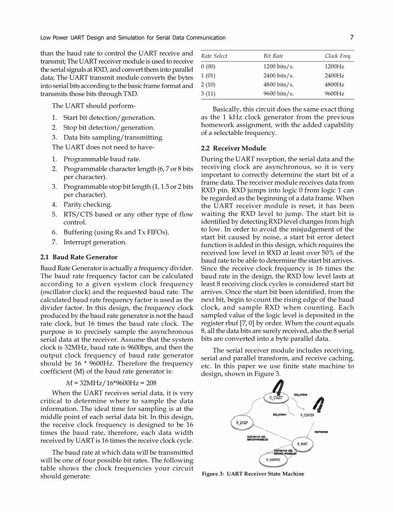
2.2 Receiver Module
During the UART reception, the serial data and thereceiving clock are asynchronous, so it is veryimportant to correctly determine the start bit of aframe data. The receiver module receives data fromRXD pin. RXD jumps into logic 0 from logic 1 canbe regarded as the beginning of a data frame. Whenthe UART receiver module is reset, it has beenwaiting the RXD level to jump. The start bit isidentified by detecting RXD level changes from highto low. In order to avoid the misjudgement of thestart bit caused by noise, a start bit error detectfunction is added in this design, which requires thereceived low level in RXD at least over 50% of thebaud rate to be able to determine the start bit arrives.Since the receive clock frequency is 16 times thebaud rate in the design, the RXD low level lasts atleast 8 receiving clock cycles is considered start bitarrives. Once the start bit been identified, from thenext bit, begin to count the rising edge of the baudclock, and sample RXD when counting. Eachsampled value of the logic level is deposited in theregister rbuf [7, 0] by order. When the count equals8, all the data bits are surely received, also the 8 serialbits are converted into a byte parallel data.
The serial receiver module includes receiving,serial and parallel transform, and receive caching,etc. In this paper we use finite state machine todesign, shown in Figure 3.
Rate Select Bit Rate Clock Freq.
0 (00) 1200 bits/s. 1200Hz
1 (01) 2400 bits/s. 2400Hz
2 (10) 4800 bits/s. 4800Hz
3 (11) 9600 bits/s. 9600Hz
Figure 3: UART Receiver State Machine
8 Neeraj Jain and Seema Sharma
The state machine includes five states:
R_START (waiting for the start bit),R_CENTER (find midpoint), R_WAIT (waiting forthe sampling), R_SAMPLE (sampling), andR_STOP (receiving stop bit).
1. R_START Status-
When the UART receiver is reset, the receiver statemachine will be in this state. In this state, the statemachine has been waiting for the RXD level to jumpover from logic 1 to logic 0, i.e. the start bit. Thisalerts the beginning of a new data frame. Once thestart bit is identified, the state machine will betransferred to R_CENTER state. In Figure 3,RXD_SYNC is a synchronization signal of RXD.Because when sampling logic 1 or logic 0, we donot want the detected signal to be unstable. So wedo not directly detect RXD signal, but detect thesynchronization signal RXD_SYNC.
2. R_CENTER Status-
For asynchronous serial signal, in order to detectthe correct signal each time, and minimize the totalerror in the later data bits detection. Obviously, it isthe most ideal to detect at the middle of each bit. Inthis state, the task is to find the midpoint of each bitthrough the start bit. The method is by counting thenumber of bclkr (the receiving clock frequencygenerated by the baud rate generator) (RCNT16 isthe counter of bclkr). In addition, the start bitdetected in the R_START may not be a really startbit, it may be an occasional interference sharp pulse(negative pulse). This interference pulse cycle is veryshort. Therefore, the signal that maintains logic 0over 1 / 4 bit time must be a start bit.
3. R_WAIT Status-
When the state machine is in this state, waiting forcounting bclkr to 15, then entering into R_SAMPLEto sample the data bits at the 16th bclkr. At the sametime determining whether the collected data bitlength has reached the data frame length(FRAMELEN). If reaches, it means the stop bitsarrives. The FRAMELEN is modifiable in the design(using the Generic). In this design it is 8, whichcorresponds to the 8-bit data format of UART.
4. R_SAMPLE Status-
Data bit sampling. After sampling the state machinetransfers to R_WAIT state unconditionally, waits forthe arrival of the next start bit.
5. R_STOP Status-
Stop bit is either 1 or 1.5, or 2. State machine doesn’tdetect RXD in R_STOP, but output frame receivingdone signal (REC_DONE <= ‘1‘). After the stop bit,state machine turns back to R_START state, waitingfor the next frame start bit.
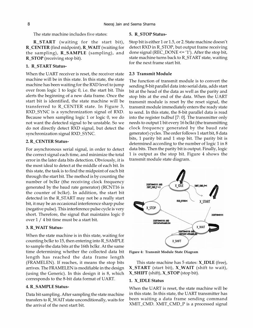
2.3 Transmit Module
The function of transmit module is to convert thesending 8-bit parallel data into serial data, adds startbit at the head of the data as well as the parity andstop bits at the end of the data. When the UARTtransmit module is reset by the reset signal, thetransmit module immediately enters the ready stateto send. In this state, the 8-bit parallel data is readinto the register txdbuf [7: 0]. The transmitter onlyneeds to output 1 bit every 16 bclkt (the transmittingclock frequency generated by the baud rategenerator) cycles. The order follows 1 start bit, 8 databits, 1 parity bit and 1 stop bit. The parity bit isdetermined according to the number of logic 1 in 8data bits. Then the parity bit is output. Finally, logic1 is output as the stop bit. Figure 4 shows thetransmit module state diagram.
Figure 4: Transmit Module State Diagram
This state machine has 5 states: X_IDLE (free),X_START (start bit), X_WAIT (shift to wait),X_SHIFT (shift), X_STOP (stop bit).
1. X_IDLE Status
When the UART is reset, the state machine will bein this state. In this state, the UART transmitter hasbeen waiting a data frame sending commandXMIT_CMD. XMIT_CMD_P is a processed signal
Low Power UART Design and Simulation for Serial Data Communication 9
of XMIT_CMD, which is a short pulse signal. SinceXMIT_CMD is an external signal, outside FPGA, itspulse width is unable to be limited. If XMIT_CMDis valid, it is still valid after sending one UART dataframe. Then the UART transmitter will think bymistake that a new data transmit command hasarrived, and once again start the frame transmit.Obviously the frame transmit is wrong. Here welimit the pulse width of XMIT_CMD. XMIT_CMD_Pis its processed signal. When XMIT_CMD_P = ‘1‘,the state machine transferred to X_START, get readyto send a start bit.
2. X_START Status-
In this state, sends a logic 0 signal to the TXD forone bit time width, the start bit. Then the statemachine transferred to X_WAIT state. XCNT16 isthe counter of bclkt.
3. X_WAIT Status-
Similar with the R_WAIT of UART receive statemachine.
4. X_SHIFT Status-
In this state, the state machine realizes the parallelto serial conversion of outgoing data. Thenimmediately return to X_WAIT state.
5. X_STOP Status-
Stop bit transmit state. When the data frametransmit is completed, the state machine transferredto this state, and sends 16 bclkt cycle logic 1 signal,that is, 1 stop bit. The state machine turns back toX_IDLE state after sending the stop bit, and waitsfor another data frame transmit command.
3. SIMULATION OF MODULE
The simulation software is Quartus II. And theselected device is Altera’s Cyclone II FPGA:EP2C5F256C6.
3.1 Baud Rate Generator Simulation
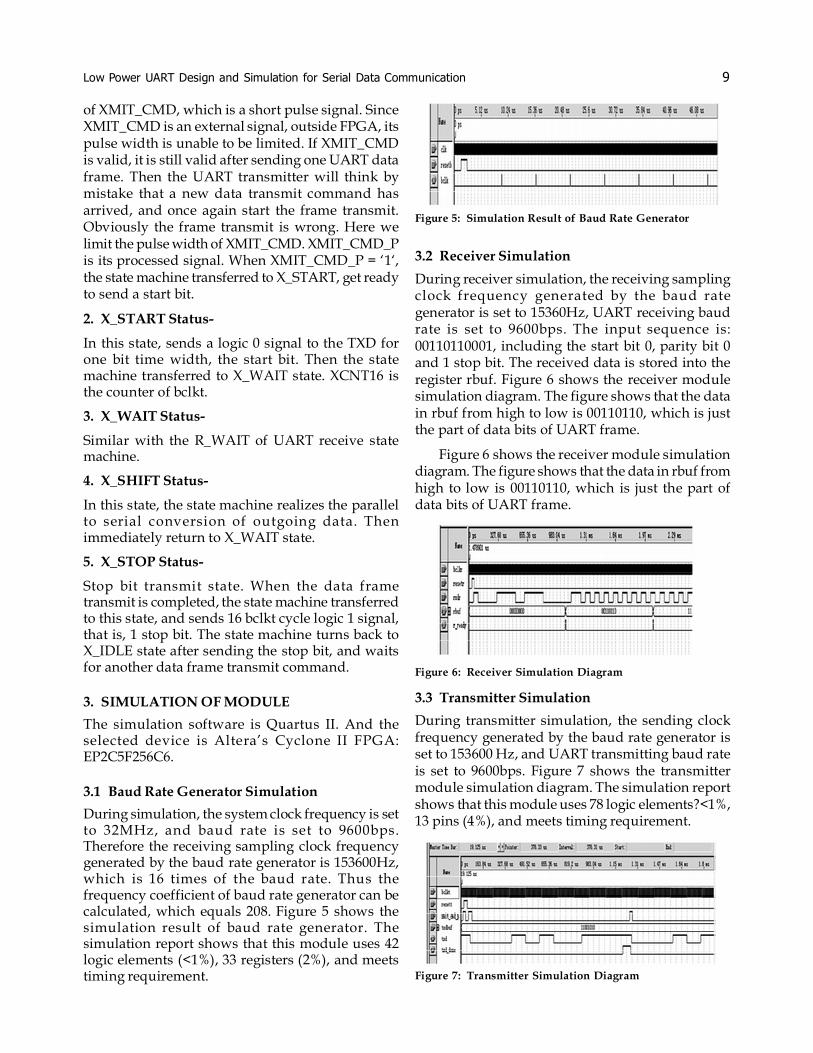
During simulation, the system clock frequency is setto 32MHz, and baud rate is set to 9600bps.Therefore the receiving sampling clock frequencygenerated by the baud rate generator is 153600Hz,which is 16 times of the baud rate. Thus thefrequency coefficient of baud rate generator can becalculated, which equals 208. Figure 5 shows thesimulation result of baud rate generator. Thesimulation report shows that this module uses 42logic elements (<1%), 33 registers (2%), and meetstiming requirement.
3.2 Receiver Simulation
During receiver simulation, the receiving samplingclock frequency generated by the baud rategenerator is set to 15360Hz, UART receiving baudrate is set to 9600bps. The input sequence is:00110110001, including the start bit 0, parity bit 0and 1 stop bit. The received data is stored into theregister rbuf. Figure 6 shows the receiver modulesimulation diagram. The figure shows that the datain rbuf from high to low is 00110110, which is justthe part of data bits of UART frame.
Figure 6 shows the receiver module simulationdiagram. The figure shows that the data in rbuf fromhigh to low is 00110110, which is just the part ofdata bits of UART frame.
Figure 5: Simulation Result of Baud Rate Generator
Figure 6: Receiver Simulation Diagram
3.3 Transmitter Simulation
During transmitter simulation, the sending clockfrequency generated by the baud rate generator isset to 153600 Hz, and UART transmitting baud rateis set to 9600bps. Figure 7 shows the transmittermodule simulation diagram. The simulation reportshows that this module uses 78 logic elements?<1%,13 pins (4%), and meets timing requirement.
Figure 7: Transmitter Simulation Diagram
10 Neeraj Jain and Seema Sharma
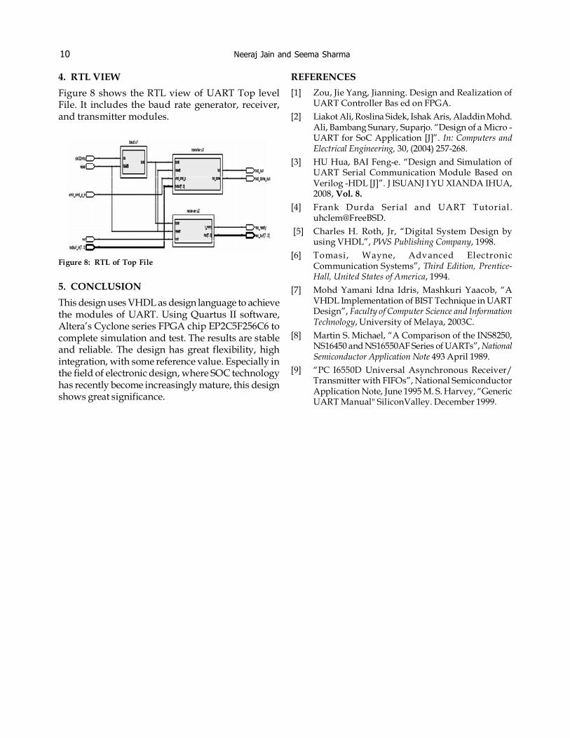
4. RTL VIEW
Figure 8 shows the RTL view of UART Top levelFile. It includes the baud rate generator, receiver,and transmitter modules.
REFERENCES
[1] Zou, Jie Yang, Jianning. Design and Realization ofUART Controller Bas ed on FPGA.
[2] Liakot Ali, Roslina Sidek, Ishak Aris, Aladdin Mohd.Ali, Bambang Sunary, Suparjo. “Design of a Micro -UART for SoC Application [J]”. In: Computers andElectrical Engineering, 30, (2004) 257-268.
[3] HU Hua, BAI Feng-e. “Design and Simulation ofUART Serial Communication Module Based onVerilog -HDL [J]”. J ISUANJ I YU XIANDA IHUA,2008, Vol. 8.
[4] Frank Durda Serial and UART Tutorial.uhclem@FreeBSD.
[5] Charles H. Roth, Jr, “Digital System Design byusing VHDL”, PWS Publishing Company, 1998.
[6] Tomasi, Wayne, Advanced ElectronicCommunication Systems”, Third Edition, Prentice-Hall, United States of America, 1994.
[7] Mohd Yamani Idna Idris, Mashkuri Yaacob, “AVHDL Implementation of BIST Technique in UARTDesign”, Faculty of Computer Science and InformationTechnology, University of Melaya, 2003C.
[8] Martin S. Michael, “A Comparison of the INS8250,NS16450 and NS16550AF Series of UARTs”, NationalSemiconductor Application Note 493 April 1989.
[9] “PC I6550D Universal Asynchronous Receiver/Transmitter with FIFOs”, National SemiconductorApplication Note, June 1995 M. S. Harvey, “GenericUART Manual" SiliconValley. December 1999.
Figure 8: RTL of Top File
5. CONCLUSION
This design uses VHDL as design language to achievethe modules of UART. Using Quartus II software,Altera’s Cyclone series FPGA chip EP2C5F256C6 tocomplete simulation and test. The results are stableand reliable. The design has great flexibility, highintegration, with some reference value. Especially inthe field of electronic design, where SOC technologyhas recently become increasingly mature, this designshows great significance.


![[PPT]UART and UART Driver - University at Buffalobina/cse321/fall2009/UARTDriver.ppt · Web viewUART and UART Driver B. Ramamurthy * UART UART: Universal Asynchronous Receiver/Transmitter](https://img.pdfslide.us/doc/110x75/5b2ab3637f8b9a55068b752f/pptuart-and-uart-driver-university-at-binacse321fall2009uartdriverppt.jpg)