Embed Size (px)
Citation preview

Low-power Sensor Interfacing and MEMS for Wireless Sensor Networks 1
Low-power Sensor Interfacing and MEMS for Wireless Sensor Networks
J.A. Michaelsen, J.E. Ramstad, D.T.Wisland and O. Søråsen
0
Low-power Sensor Interfacing and
MEMS for Wireless Sensor Networks
J.A. Michaelsen, J.E. Ramstad, D.T. Wisland and O. SøråsenNanoelectronic Systems Group, Department of Informatics, University of Oslo
Norway
1. Introduction
The need for low-power and miniaturized electronics is prominent in wireless sensor network(WSN) nodes—small sensor nodes containing sensors, signal processing electronics, and aradio link. The demand for long battery life of such systems, especially if used in biomedicalimplants or in autonomous installations, forces the development of new circuit topologiesoptimized for this application area. Through a combination of efficient circuit topologies andintelligent control systems, keeping the radio idle when signal transmission is not needed, theradio link budget may be dramatically reduced. However, due to the demands for continuouslymonitoring of the sensor in many critical applications, the sensor front-end, analog-to-digitalconverter (ADC), and the control logic handling the radio up/down-link may not be turned off,and for systems with long intervals between transmissions, the energy consumed by these partswill have a large impact on battery life. In this chapter, we focus on Frequency ∆Σ Modulator(FDSM) based ADCs because of their suitability in WSN applications. Using FDSM basedconverters, both sensors with analog and frequency modulated outputs may be convenientlyinterfaced and converted to a digital representation with very modest energy requirements.Microelectromechanical systems (MEMS) integrated on-die with CMOS circuitry enables verycompact WSN nodes. MEMS structures are used for realizing a wide range of sensors, and formvital components in radio circuits, such as mixers, filters, mixer-filters, delay lines, varactors,inductors, and oscillators. In this chapter a MEMS oscillator will be used to replace VoltageControlled Oscillators (VCOs). The MEMS oscillator is made using a post-CMOS process.Before the die is packaged, the CMOS die is etched in order to release the MEMS structures.The top metal layers in the CMOS process acts as a mask to prevent CMOS circuitry from beingetched in addition to be used as a mask to define the MEMS structures. The resulting MEMSstructure consists of a metal-dielectric stack where its thickness is determined by the numberof metal layers available in the CMOS process. In this chapter, we will use a deep sub-micronCMOS process to illustrate the possibility for combining MEMS and CMOS in a small die area.The MEMS oscillator is to be used as a frontend for the FDSM.FDSM and MEMS integrated in CMOS is a versatile platform for miniaturized low-power WSNnodes. In this chapter we illustrate the benefits of this approach using simulation, showing thepotential for efficient miniaturized solutions.
1
www.intechopen.com

2. Background
Within the international research community and industry, large research and developmentefforts are taking place within the area of Wireless Sensor Networks (WSN) (Raghunathan et al.,2006). Wireless sensor nodes are desirable in a wide range of applications. From a researchperspective, power consumption and size are main parameters where improvements areneeded. In this chapter we will focus on methods and concepts for low-voltage and low-powercircuits for sensor interfacing in applications where the power budget is constrained, along withMEMS structures suitable for on-die CMOS integration. These technologies enable wirelesssensor network nodes (WSNNs) with a very compact size capable of being powered with adepletable energy source due to its potential for low voltage and low power consumption.
Sensor ADC DSP TX
Fig. 1. Wireless sensor network node
The key components of a wireless sensor node are: 1) The sensor performing the actual mea-surement (pressure, light, sound, etc.), producing a small analog voltage or current. 2) Ananalog-to-digital (A/D) converter (ADC) converting and amplifying the weak analog sensoroutput to a digital representation. 3) A digital signal processing system, performing local com-putations on the aquired data to ready it for transmission, and for deciding when to transmit.4) A radio transceiver for communicating the measurements. This is depicted in figure 1. Thesensor readout circuitry, namely the ADC and processing logic, must continuously monitor thesensor readings in order to detect changes of interest and activate the transceiver only whenneeded to conserve power. For digital CMOS circuitry, an efficient way of saving power is toreduce the supply voltage, resulting in subthreshold operation of MOSFET devices, as theirconductive channel will only be weakly inverted (Chen et al., 2002). In standard nanometerCMOS technology, safe operation is possible with supply voltages down to approximately200mV (Wang & Chadrakasan, 2005). Conventional analog circuit topologies are not ableto operate on these ultra low supply voltages, especially with the additional constraint ofa scarce power budget (Annema et al., 2005). As a result, the ADCs currently represents acritical bottleneck in low-voltage and low-power systems, accentuating the need for new designmethodologies and circuit topologies.The sensor readout circuit must satisfy certain specifications like sufficient gain, low distortionand sufficient signal-to-quantization-noise ratio (SQNR). When studying existing Nyquist-rate ADCs, it is obvious that the analog precision is reduced as the power supply voltageis lowered (Chatterjee et al., 2005). This is mainly due to non-ideal properties of the activeand passive elements, and process variations. In order to increase the SQNR, oversampledconverters employing noise shaping ∆Σ modulators are used, trading bandwidth for higherSQNR (Norsworthy et al., 1996). ADCs are implemented either using continuous-time (CT) orSwitched Capacitor (SC) components for realizing the necessary analog filter functions. SCrealizations have generally been preferred for CMOS implementations as the method doesnot rely on absolute component values which are difficult to achieve without post-fabricationtrimming. During the last few years, the power supply has moved down to 1 V in state-of-theart technologies making it hard to implement switches with sufficient conduction requiredfor SC-filters. As a result, current SC realizations switch the opamp, eliminating the need
www.intechopen.com

Low-power Sensor Interfacing and MEMS for Wireless Sensor Networks 3
for CMOS switches in the signal path. This method is referred to as the Switched Opamptechnique (Sauerbrey et al., 2002). As a result, the most important building block for bothCT and SC based ∆Σ modulators are the opamp, which is also the limiting component withrespect to conversion speed and signal-to-noise and distortion ratio (SINAD). As mentionedearlier, the sensor readout circuitry in a battery operated wireless sensor node should allow foroperation far below 1V to facilitate low power consumption. This requirement eliminates bothconventional CT and SC ∆Σ modulators as these approaches require large amounts of powerat low supply voltages to attain reasonable performance.Several low-power ADC topologies adapted for sensor interfacing have been reported in thelast few years (Yang & Sarpeshkar, 2005; Kim & Cho, 2006; Wismar et al., 2007; Taillefer &Roberts, 2007). Among them, some are utilizing the time-domain instead of the amplitude-domain to reduce the sensitivity to technology and power supply scaling (Kim & Cho, 2006;Wismar et al., 2007; Taillefer & Roberts, 2007).The non-feedback modulator for A/D conversion was introduced in Høvin et al. (1995); Høvinet al. (1997). In contrast to earlier published ∆Σ based ADCs, this approach does not requirea global feedback to achieve noise shaping giving new and additional freedom in practicalapplications. This property is particularly useful when the converter is interfacing a sensor(Øysted & Wisland, 2005). The non-feedback ∆Σ modulator has two important propertieswhich make it very suitable for low-voltage sensor interfacing. First, the topology has no globalfeedback which opens up for increasing the speed and resolution compared to conventionalmethods. Second, and most important, the analog input voltage is converted to an accumulatedphase representing the integral of the input signal, thus moving the accuracy requirementsfrom the strictly limited voltage domain, to the time domain, which is unaffected by the supplyvoltage. The conversion from analog input voltage to accumulated phase is performed using aVoltage Controlled Oscillator (VCO). As this solution uses frequency as an intermediate value,the non-feedback ADC using a VCO for integration is normally referred to as a FrequencyDelta Sigma Modulator (FDSM).Until recently, the FDSM has mainly been used for converting frequency modulated sensorsignals with no particular focus on low supply voltage. In Wismar et al. (2006), an FDSMbased ADC, fabricated in 90 nm CMOS technology, is reported to operate properly down toa supply voltage of 200 mV with a SINAD of 44.2 dB in the bandwidth from 20 Hz to 20 kHz(the audio band). The measured power consumption is 0.44 µW. The implementation is basedon subthreshold MOSFET devices with the bulk-node exploited as input terminal for the signalto be converted.At the RF front-end in WSN nodes, bulky off-chip components are usually used to meet the RFperformance requirements. Such components are typically external inductors, crystals, SAWfilters, oscillators, and ceramic filters (Nguyen, 2005). Micromachined components have beenshown to potentially replace many of these bulky off-chip components with better performance,smaller size and lower power consumption. The topic of combining MEMS directly with CMOShas been of great interest in the past years (Fedder et al., 2008). The direct integration of MEMSwith CMOS reduces parasitics, reduces the packaging complexity and the need for externalcomponents becomes less prominent. It turns out that integrating MEMS after the CMOS diehas been produced has been most successful which is proven by Carnegie Mellon University(Chen et al., 2005; Fedder & Mukherjee, 2008), National Tsing Hua University (Dai et al., 2005),University of Florida (Qu & Xie, 2007) and University of Oslo (Soeraasen & Ramstad, 2008;Ramstad et al., 2009). The concept of CMOS-MEMS is maturing and seems to be versatile and
www.intechopen.com

offer the flexibility of possibly replacing RF-front end components or sensors, both relevant inthe context of WSNN.
3. Frequency Delta-Sigma Modulators
An FDSM based converter (Høvin et al., 1997) can conveniently be used in WSNNs for convert-ing frequency modulated signals to a quantized and discrete bitstream, where the quantizationnoise is shaped away from the signal band. Overall, this results in frequency-to-digital (F/D)conversion with equivalent ∆Σ noise shaping.
· · ·∫
·dτ + d·dt
· · ·
eq
Fig. 2. FDSM overview
In the time domain, the input to the modulator, a frequency modulated (FM) signal, is xfm(t) =cos[θ(t)], where the instantaneous phase is,
θ(t) = 2π
∫ t
0fc + fd · x(τ)dτ (1)
fd is the maximal deviation from the carrier frequency, fc, while x(τ) represents the physicalquantity we are measuring; assumed to be limited to ±1. The integral of the input signal anda constant bias is now represented by the phase, θ(t). The cosine function wraps the phaseevery 2π, effectively performing modulo integration. By using a counter, triggered by thezero-crossings of the xfm signal, the integral of the input signal is quantized to a digital valuewhich in turn is sampled at regular intervals, Ts = f−1
s . A digital representation of the input,x, is recovered by differentiating the quantized phase signal. This is depicted in figure 3(a).
−
+Register
Register
Counter
nn
nClk
Clkxfm
y1
(a) multi-bit
DFF
Q
CK
D
DFF
Q
CK
D y1
xfm
Clk
(b) single-bit (DFF)
Fig. 3. First order FDSM topologies
www.intechopen.com

Low-power Sensor Interfacing and MEMS for Wireless Sensor Networks 5
0.005 0.01 0.05 0.1fc/ fs
20
30
40
50
60
SQ
NR
(dB
)
··
·
··· ·
· · · ··
· ·
··········
·
·
····
······
·
···
Fig. 4. Theoretical performance (solid line) and time-domain simulated performance (dots) as afunction of carrier frequency and sampling frequency ratio
An important property is that quantization noise occurs after the integration, resulting in firstorder noise shaping of the quantization noise sequence, while the input signal is not altered.This is illustrated in figure 2, where eq represents the quantization noise. Second order noiseshaping can be obtained by integrating the quantization error from the first order FDSM. Whilethe second order system requires a higher circuit complexity which incurs an increase in powerconsumption, it can be shown that the increase in performance in some cases outweighs theadditional requirements (Michaelsen & Wisland, 2008).The FDSM is inherently an oversampled system, meaning that the output bitrate, fs, is muchhigher than the bandwidth of the input signal, fb. Quantization noise is suppressed in thesignal band through noise shaping. In the case of first order converters, the quantization noisewill be shaped with a slope of 20 dB/decade.If the number of zero-crossings of the FM signal during Ts is less than two, it is possible torealize the structure in figure 3(a) with only two D-flipflops (DFFs), and an XOR-gate usedfor subtraction, as illustrated in figure 3(b). Due to its simple implementation, the first ordersingle-bit FDSM is a viable choice for WSNN applications because of its potential for low powerconsumption and low voltage operating requirements (Wismar et al., 2007). In this case, theresolution of the converter is given by (Høvin et al., 1997)
SQNRdB = 20log10
(√2 fd
fs
)
− 10log10
(
π2
36
(
2 fb
fs
)3)
(2)
However, in cases where fs/ fc ≫ 1, the actual performance may be better than predictedby equation 2. As illustrated in figure 4, this discrepancy can be significant. In this plot, fs
was held constant at 20 MHz, with fd = fc · 10%, and fb = 19 kHz. The solid line representsthe performance predicted by equation 2 while the dots indicate the performance from adifference equation simulation of the converter. The underlying assumption in equation 2 isthat the quantization noise sequence is a white noise sequence. However, this assumptionin not accurate, and it is possible to exploit pattern noise valleys for significantly improvingperformance (Høvin et al., 2001).
www.intechopen.com

Before further processing of the digital sensor signal in the WSNN, it is usually desirable tohave an output frequency that is equal to, or slightly higher than, 2 fb. To achieve this the outputbitstream is decimated by first bandlimiting the signal using a low-pass filter. This removes theout-of-band noise to avoid aliasing. After low-pass filtering, only every N-th sample is kept,where N = fs/2 fb
. During and after decimation, each sample must be represented by more bitsto avoid quantization noise being a limiting factor. The decimation usually requires a significantamount of computation. This task is therefore done in stages, where computationally efficientfilters run at the input frequency, while more accurate filters run at lower frequencies. The firststage is usually a sincm-filter, where m is the order of the filter, named after its (sin(x)/x)m
shaped frequency response. This class of filter has a straight forward hardware implementation(Hogenauer, 1981; Gerosa & Neviani, 2004) capable of high frequency operation. It can beshown that a sincL+1 filter is sufficient for an order L ∆Σ modulator (Schreier & Temes, 2004).At later stages, more complex filters can be used to correct for the non-ideal features of the sincfilter such as passband droop (Altera Corporation, 2007).The frontend of the FDSM—be it a VCO in the case of an ADC, or a device which directlyconverts some physical quantity to a frequency modulated signal—will to some extent havea non-linear transfer function. A non-linear FM source will in turn give rise to harmonicdistortion present in the output signal. Although quantization noise is shaped away fromthe signal band, harmonic distortion will not be suppressed as it is impossible for the F/Dconverter to distinguish between what is the actual signal and what is noise and distortion.This non-linearity deteriorates the effective resolution of the measurement system. However,several digital post-processing schemes and error correction systems have been devised thatare able to recover linearity to some extent (Balestrieri et al., 2005). Care must be taken whendesigning the post-processing system so that aliasing of values and missing output codes doesnot present a problem. Another issue with the FDSM frontend is phase noise, also referred to asjitter. This noise will directly add to the input signal and therefore not undergo noise shaping;raising the noise floor at the output. 1/f noise has shown to be particularly problematic, andcareful attention to issues related to noise is critical when designing the oscillator circuit. Thisis especially challenging in deep sub-micron CMOS technologies.
4. Using a MEMS resonator as a VCO
4.1 The micromechanical resonator
A resonator is a component which is able to mimic full circuit functions such as filtering, mixing,line delays, and frequency locking. The resonator is a mechanical element that vibrates backand forth where the displacement of the micromechanical element generates a time varyingcapacitance which in turn results in an ac current at the output node. The maximum outputcurrent occurs when stimulating the resonator with an input ac voltage with a frequency equalto the resonance frequency of the resonator. The micromechanical resonator can be representedas an LCR circuit (see figure 5) where the equations describing these passive components arerelated to physical parameters such as mass, damping, and stiffness (Senturia, 2001; Bannonet al., 2000).Figure 5 is a simple LRC circuit which can be described as,
Vi = q(t)Lx + q(t)Rx + q(t)1
Cx(3)
where Lx, Rx and Cx are the passive element values for a maximum displacement x of theresonator. Vi and Vo are the input and output voltages as shown in figure 5. q(t) is the charge
www.intechopen.com

Low-power Sensor Interfacing and MEMS for Wireless Sensor Networks 7
C
RL
ViVo
x x
x
Fig. 5. A simple LCR circuit
on the capacitor which depends on the time t. By using the relationship between the outputand the input (H(t) = Vo/Vi) from the circuit of figure 5 and by using q = CxV results in thederivation of the resonance frequency of this system:
f0 =1
2π
√
1
LxCx(4)
From the transfer function, the maximum throughput exists when the reactances of the inductorand the capacitor is equal to each other and opposite, thus this defines the resonance frequencyfor this micromechanical system. For RF front-end components and oscillators, it is desirableto have a good transfer of the signal through the component. A good throughput is possible byhaving a good Q-factor which is described by,
Q =ω0Lx
Rx(5)
where equation 5 is derived from the transfer function of figure 5 and ω0 is the resonancefrequency of the resonator (ω0 = 2π f0). A large Q-factor is usually desirable to get goodresonator performance. As explained in section 4.5, the resulting MEMS structures consists of alaminate of metal and dielectric, so the resulting Q-factor will be limited mostly by intrinsicmaterial loss and gas damping which will be discussed later. A top view of a micromechanicalresonator is shown in figure 6.
In
V
Layout view
Stationary structure
or anchor
Movable structure
C RL xx x
Equivalent passive components
in a schematic view
In Out
x
y
=Out
P
Fig. 6. The resonator analogy
Figure 6 shows a long and thin cantilever beam (fixed at one end, free to move at the otherend) with two electrodes next to it. The left electrode is the input electrode while the rightelectrode is the output electrode. The gray areas indicate stationary elements (the anchor and
www.intechopen.com

the electrodes) while the blue area indicates a part which is able to move freely (the resonator).The thin and long cantilever beam moves back and forth laterally above the silicon substratetowards the two electrodes in the x-direction. At the resonance frequency of this resonator, themaximum vibration towards the electrode is x. The thickness of the beam is not shown here asthis is a top view. The VP signal applied to the beam itself is a high DC voltage which is usedto cancel unwanted frequency terms and to amplify the signal of the resonator. By separatingthe VP signal from the input and output ac signals, the VP signal will not be superimposed oneither of the two signals. The gap g between the resonator and the electrodes is an importantparameter which will decide vital aspects of the resonator as will be shown later.
4.2 The electromechanical analogy
4.2.1 The electromechanical coupling coefficient
The micromechanical resonator is attracted due to electrostatic forces creating a capacitivecoupling between the resonator and the input electrode (Kaajakari et al., 2005). A large electrodearea that covers the resonator is desirable where the capacitance C is described as,
C =ε0WrWe
g(6)
where ε0 is the permittivity in air, Wr is the resonator width (vertical thickness, not visible infigure 6), We is the electrode length, and g is the gap between the resonator and the electrode.The capacitance equation is related to the electrostatic force equation (F). The electrostatic forceF is derived from the potential energy equation U = 1/2CV2 which results in:
F =dU
dx=
1
2
dC
dxV2 (7)
where V is the signal voltage. dC/dx is the capacitance change due to a small change in the gapsize g because the resonator bends towards the electrode with a displacement x. The force isproportional to the square of the voltage V which will introduce a cos(2ωt) term (the derivationof this is not shown here). The cos(2ωt) term will introduce oscillation at ω = ω0/2, half theresonance frequency. In order to avoid this nonlinear relationship, a polarization voltage VP
is applied to the beam. When splitting V into VP + v · cos(ωt) the resulting electrostatic forcebecomes,
f = VPdC
dxv (8)
Equation 8 describes the relationship between the force f and the voltage v (small signal values)that now has a linear relationship. It is now possible to derive the coefficient known as η:
η = VPdC
dx≈ VP
ε0WrWe
g2(9)
η is a coefficient which describes how well the signal from the electrode is transferred to theresonator. It is an equation that is a result of the electrostatic force equation so that the force fhas a linear relationship to the voltage v. A larger η results in a larger signal of the resonator. Itis desirable with a large electrode area (Ael = WrWe) and a small gap g. Because η is inverselyproportional to the square of the gap between the electrode and resonator, it is desirable tohave an extremely small gap size. Both the electrode area Ael and the gap size g are limitedby process constraints. Notice that equation 9 is a simplified equation of η as the derivationof the capacitance C with respect on the gap g is done by assuming that the gap is the samethroughout the y-axis of the resonator (throughout the resonator length L).
www.intechopen.com
Low-power Sensor Interfacing and MEMS for Wireless Sensor Networks 9
4.2.2 Resonator output current
The output current due to the capacitive coupling explained in section 4.2.1 can be written as:
io = VPdC
dt+ C
dv
dt≈ VP
dC
dt(10)
The output current in equation 10 consists of two parts: One part which is amplified withthe polarization voltage VP, and one part which consists of the (small) sinusoidal voltage v.Equation 10 was derived by using io = d/dt(C · V) (Bannon et al., 2000). It is possible to furthersimplify this equation by neglecting the C dv/dt part because the voltage VP is much larger thanv:
io = VPdC
dx
dx
dt≈ ηω0x (11)
Equation 11 was derived by using the relationship dx/dt = ω0x. By using VP, the output currentio can be amplified as shown in equation 11. However, when increasing VP, ω0 will be reducedwhile the displacement x increases. This means that the current will have an exponential-likeincrease as VP is increased and not a linear increase of io which could be expected. The factthat the operational (resonance) frequency of the resonator decreases when VP is increased isdue to an effect known as "spring-softening" which will be discussed later (Bannon et al., 2000).This spring-softening effect will be utilized in order to use the micromechanical resonator as avoltage-controlled oscillator (VCO).
4.2.3 The LCR equivalents
By using the principle of electromechanical conversion as explained in section 4.2.1, it ispossible to derive formulas for Lx, Cx and Rx.
Lx =meff
η2(12)
Cx =η2
kr(13)
Rx =
√
krmeff
Qη2(14)
where kr is the effective spring stiffness and meff is the effective mass of the resonator. Qis the Q-factor of the resonator which is inverse proportional to the total damping of themicromechanical resonator. All three LCR components are dependent on the square of η.This indicates a square dependence of the electrode area Ael and a g4 dependence of the gapbetween the resonator and the electrode. The electrical equivalents of the components are notstraightforward to interpret due to complicated relationships between the mass, stiffness anddamping of the resonator, as well as complicated relationship due to the electrostatic force.
4.3 The resonance frequency and its implications
4.3.1 The nominal resonance frequency
The natural frequency of the resonator with no voltage applied is given by equation 15 below(Senturia, 2001):
f0(eff ) =1
2π
√
Λnk
m(15)
www.intechopen.com

where k is the static beam stiffness and m is the static beam mass of the micromechanical system.Λn is a constant depending on mode number. A mode is a certain frequency in which theresonator will have a maximum vibration amplitude. A micromechanical resonator may haveseveral modes at distinct frequencies. Λn has different values for different modes. For example,Λ1=1.0302 for mode 1, Λ2=40.460 for mode 2, Λ3=317.219 for mode 3 etc. The resonator isoperated in the first mode (Λ1). Both k and m depends on the geometry and structural materialof the resonator. The values for Λn used here is valid only for the cantilever beam architecture,other types of resonators will have different values of Λn.
4.3.2 The effective resonance frequency and Q-factor
The movable parts of the resonator will all vibrate back and forth with the resonance frequencyω0. The tip of the beam will have a longer distance to move and will thus have a higher velocityv compared to the part of the cantilever beam which is closer to the anchor. Because the kineticenergy (Ek =
1/2meff v2) must be the same throughout the beam when it vibrates, the effectivemass along the beam in the y-direction in figure 6 will vary. The effective mass is defined asmeff where the largest value appears close to the anchor while the smallest value appears atthe tip of the beam. The derivation of meff is not shown here but can be developed by usingthe equation for kinetic energy. By using equation 15 and rearranging, the mechanical springstiffness can be defined as:
km(y) =(
2π f0(eff )
)2meff (y) (16)
Equation 16 shows the pure mechanical spring stiffness of the beam when it vibrates. km(y)varies along the beam in the y-direction with a maximum value close to the anchor and aminimum value close to the tip of the beam. However, when applying a DC voltage VP tothe beam, the total spring stiffness of the beam will be reduced. The resulting effective springstiffness value kr is reduced due to an electric spring value ke. Because of this fact, the resonancefrequency of the cantilever beam will be reduced as described in the following equation:
f0 = f0(eff )
√
1 −ke
km(17)
where the relationship ke/kmdetermines the amount of reduction of the original nominal
resonance frequency f0(eff ). The effective spring stiffness kr is defined as:
kr = km − ke (18)
where kr is known as the effective beam stiffness. kr is the result of subtracting the electricalspring stiffness ke from the effective mechanical spring stiffness km (spring-softening). Theeffective beam stiffness is more precisely defined as,
kr =(
2π f0(eff )
)2meff (y)−
∫ We2
We1
V2P
ε0Wrdy′
[g(y′)]3(19)
where the second term of equation 19 describes the electrical spring stiffness at a specificlocation y′ centered on an infinitesimal length of the electrode dy′. The ke part consists ofintegrating from the start of the electrode (We1) to the end of the electrode (We2). The variablepart of the ke equation is the gap which varies along the y-axis throughout the beam length. The
www.intechopen.com

Low-power Sensor Interfacing and MEMS for Wireless Sensor Networks 11
ke equation is derived from the potential energy equation U = 1/2CV2P . The gap as a function
of y can be described as (Bannon et al., 2000):
g(y) = g0 −1
2V2
P ε0Wr
∫ We2
We1
1
km(y′)[g(y′)]2Xmode(y)
Xmode(y′)dy′ (20)
where g0 is the static electrode-to-resonator gap with VP = 0. Xmode is an equation that describesthe shape of how the cantilever beam bends. The second term describes the displacementof the resonator towards the electrode at various locations of y. As can be seen in equation18, if ke becomes equal to km, the resonance frequency should become zero. However, beforethat would occur, the resonator will enter an unstable state which will pull the beam towardsthe electrode instead. This effect is known as the "pull-in" effect. Due to the reduction ofthe original natural frequency of the resonator, the Q-factor will also be reduced in a similarmanner. The Q-factor is mainly affected by four factors: Anchor loss, environmental (viscousgas) damping, thermoelastic damping or internal (material) energy loss. The topic of dampingmechanisms for MEMS resonators is not trivial, therefore it is typical to do crude estimates forthe nominal Q-factor as a starting point for analysis (Bannon et al., 2000).
Qeff = Qnom
√
1 −ke
km(21)
From equation 17 and equation 21 we can conclude that when increasing the VP value, boththe resonance frequency and the Q-factor of the resonator are reduced. For oscillators, a highQ-factor is desirable, therefore it is important to also include this reduction of the Q-factor forcorrect modeling.
4.4 Nonlinear behavior
As described by equation 17, the oscillation frequency is tuned by using VP. In order to get agood tuneability of the MEMS resonator, it is designed to be soft so that it can operate at lowvoltages and at the same time have a reasonable tuning range. However, when a beam is toosoft, non-linear effects become more dominant. We can classify two different types of resonatornon-linearities (Kaajakari et al., 2005; 2004):
• Mechanical non-linearity: Typically non-elasticity due to geometrical and material effects
• Capacitive non-linearity: Introduced due to an inverse relationship between the displace-ment and the ”parallel” plate capacitance
Mechanical non-linearity will be more prominent in other resonator architectures such asthe clamped-clamped beam, we will therefore focus on the capacitive non-linearities for thisanalysis. In order to develop an understanding of the introduction of the capacitive non-linearity, we must take a look at the equation describing the motion of the resonator:
meff x + bx + krx = F(t) (22)
Equation 22 describes the equation of movement of the resonator due to an external force. Thisequation is basically the same as equation 3 where the external force is the electrostatic force.The equation of movement is related to the effective mass meff , the damping b (which is inverseproportional to Q), and the effective spring stiffness kr. In this equation kr has a mechanical
www.intechopen.com

term km and an electrical term ke as described earlier. For a case where ke is linear, the motionof the amplitude becomes:
X0 =FQeff
kr(23)
Equation 23 shows the displacement of the tip of the beam at resonance. However, whenthe resonator has a low mechanical stiffness km, and is at the same time operated with largeVP values, the linear ke model becomes inaccurate. Therefore the following equation is usedinstead:
ke(x) = ke0
(
1 + ke1x + ke2x2 + ...kenxn)
(24)
From equation 24, we can see that the spring stiffness consists of higher order terms that all arerelated to the displacement x (Kaajakari et al., 2005). The ke0 term is the first term and is linear.ke1 and ke2 are square and cubic electrical spring coefficients respectively:
ke0 = −
V2PC0
g2,ke1 =
3
2g,ke2 =
2
g2(25)
The ke(x) terms contribute to reducing or increasing the frequency depending on which termthat dominates. When operating the resonator with high vibration amplitudes, the square andcubic spring stiffness terms will become more dominant. Because the amplitude-frequencycurve no longer becomes a single valued function, the oscillation may become chaotic once theamplitude is larger than a critical value known as xc. The maximum usable vibration value isextracted from the largest value that appears before a bifurcation (hysteresis of the curve). Thebifurcation amplitude and critical amplitude are respectively (Kaajakari et al., 2005):
xb =1
√√3Q|κ|
, xc =2
√
3√
3Q|κ|(26)
where
κ =3ke2ke0
8k−
5k2e1k2
e0
12k2(27)
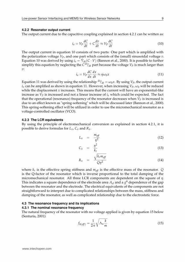
Figure 7 is an example of how κ will affect the response out from the resonator. κ1 is the lowestvalue and κ3 is the largest value. In this example, κ is positive and contributes to increase inthe resonance frequency as well as tilting the curve to the left. κ1 is the lowest value and showsless tilting of the curve. When κ is too large (see κ3), the curve enters a state of hysteresis. Atthe point when the hysteresis starts, the bifurcation amplitude xb is reached. For any curvewith a hysteresis, the maximum usable amplitude of vibration is xc as shown in figure 7b. xc isalways larger than xb and ultimately sets the limit for the maximum vibration amplitude aswell as it sets the maximum output current from the resonator. Because κ is a factor which willcontribute to a modified resonance frequency due to the spring stiffness non-linearities, thenew resonance frequency is therefore expressed as,
ω0(effective) = ω0
(
1 + κX20
)
(28)
From equations 27 and 28 we can see that κ will either increase (resonator becomes more stiff)the operational resonance frequency or decrease the resonance frequency. The resonator usedhere will have a positive κ, thus the capacitive non-linearities will contribute to stiffen the
−0.5 −0.4 −0.3 −0.2 −0.1 0 0.1 0.2 0.3 0.4 0.5
107
108
Res
pons
e
Frequency offset
1
2
3
Increasinghysteresiseffect
−0.2 −0.15 −0.1 −0.05 0 0.05 0.1 0.15 0.2
107
108
Res
pons
e
Frequency offset
xc = maximumamplitude whenthe responseshows hysteresisxb = Hysteresis
point
www.intechopen.com
Low-power Sensor Interfacing and MEMS for Wireless Sensor Networks 13
−0.5 −0.4 −0.3 −0.2 −0.1 0 0.1 0.2 0.3 0.4 0.5
107
108
Res
pons
e
Frequency offset
κ1κ2κ3
Increasinghysteresiseffect
(a) Increasing κ
−0.2 −0.15 −0.1 −0.05 0 0.05 0.1 0.15 0.2
107
108
Res
pons
e
Frequency offset
xc = maximumamplitude whenthe responseshows hysteresisxb = Hysteresis
point
(b) Hysteresis for κ3
Fig. 7. Bifurcation and critical bifurcation
resonator. Because κ contributes to ”stiffen” the output response, more VP must be applied thanfirst estimated in equation 17. By using equation 26 and 27, an expression for the maximumoutput current possible from the resonator is developed:
imaxo = ηω0xc (29)
imaxo sets the limit for how much current that can be registered at the output electrode before
bifurcation. The difference between equation 10 and equation 29 is that the maximum currentis limited by the critical vibration xc instead. It is also possible to define the maximum energystored in the resonator by using xc in a similar manner.
Emaxstored =
1
2k0x2
c (30)
where k0 is a linear spring constant (k0 = km − ke0). The maximum energy stored also deter-mines the energy dissipation out from the resonator which is,
Pdissipated = Rxi2o =ω0Emax
stored
Q(31)
In order to understand the stability of the resonance frequency, the phase-noise of the systemcan be evaluated. This is possible by using Leeson’s equation to model the phase-noise-to-carrier ratio in an ideal oscillator:
L(∆ f ) = 10log
[
kT
πEmaxstored
Q
f0
(
1 +
(
f0
2Q∆ f
)2)]
(32)
where k is Boltzmann’s constant and T is the absolute temperature (Shao et al., 2008). It iscommon to relate equation 32 to equation 31 and also add a buffer noise source from theamplifier following the resonator as given by (Kaajakari et al., 2004):
L(∆ω) =2kT
Pdissipated
(
ω0
2Q∆ω
)2
+P
bufferN
2Pdissipated(33)
www.intechopen.com
where PbufferN is buffer noise from an amplifier source. This value can be set to −155dBm/√
Hz
(or vn = 4n V/√Hz
for a 50Ω system). The equation for phase noise will be shown in a practicalexample in section 5.2.
4.5 Integration of MEMS in CMOS
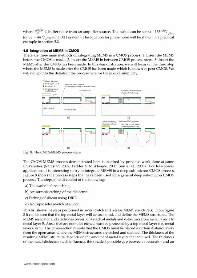
There are three main methods of integrating MEMS in a CMOS process: 1. Insert the MEMSbefore the CMOS is made. 2. Insert the MEMS in between CMOS process steps. 3. Insert theMEMS after the CMOS has been made. In this demonstration, we will focus on the third stepwhere the MEMS is made after the CMOS has been made which is known as post-CMOS. Wewill not go into the details of the process here for the sake of simplicity.
S2
E2
S
SS
Metal layer 6 or 7;shielding layer
Metal layer 5
Metal layers 1 to 4
Silicon substrate
Dielectric layers
CMOS circuitry
Remaining dielectric layers
after the first etch stepVias
Resulting silicons profile
after the third etch step
CMOS shielded by
the top metal layer
MEMS resonator structure
(stack of metal-dielectric from M1 to M5)
Released MEMS resonator
Silicon substrate
(a) (b)
(c) (d)
Fig. 8. The CMOS-MEMS process steps
The CMOS-MEMS process demonstrated here is inspired by previous work done at someuniversities (Ramstad, 2007; Fedder & Mukherjee, 2005; Sun et al., 2009). For low-powerapplications it is interesting to try to integrate MEMS in a deep sub-micron CMOS process.Figure 8 shows the process steps that have been used for a general deep sub-micron CMOSprocess. The steps a) to d) consist of the following:
a) The wafer before etching
b) Anisotropic etching of the dielectric
c) Etching of silicon using DRIE
d) Isotropic release-etch of silicon
This list shows the steps performed in order to etch and release MEMS structure(s). From figure8 it can be seen that the top metal layer will act as a mask and define the MEMS structures. TheMEMS resonator and electrodes consist of a stack of metals and dielectrics from metal layer 1 tometal layer 5. Areas that are not to be etched must be protected by a top metal layer (i.e. metallayer 6 or 7). The cross-section reveals that the CMOS must be placed a certain distance awayfrom the open areas where the MEMS structures are etched and defined. The thickness of theresulting MEMS structure depends on the amount of metal layers that are used. The thicknessof the metal-dielectric stack influences the smallest possible gap between a resonator and an
www.intechopen.com

Low-power Sensor Interfacing and MEMS for Wireless Sensor Networks 15
electrode. There are also rules which define the smallest possible width of a structure and thelargest possible width of a structure. There are more CMOS-MEMS rules than discussed here,but these are some of the most important ones when combining CMOS and MEMS on-chip bymaking MEMS structures from the metal layers offered by a general CMOS process.
4.6 The oscillator circuit
The MEMS resonator described in section 4.1 is made using a conventional 90 nm CMOSprocess using the same process steps as described in section 4.5. By putting the micromechanicalresonator in a feedback loop with an amplifier, we get the basic oscillator circuit as shown infigure 9 below:
Vout
AmplifierA
B B
RResonator
VP
VDD
Fig. 9. Basic oscillator circuit
An oscillator is defined as a circuit that produces a periodic output signal at a fixed frequency.The resonator is the element in the circuit which defines the resonance frequency while theamplifier is the active element which sustains oscillation. The bias voltage VP applied tothe resonator is used to tune the frequency of this voltage-controllable oscillator. In thisdemonstration, the Q-factor of the resulting metal-dielectric MEMS structure is lower comparedto state-of-the-art MEMS and will contribute to increase the motional impedance Rx whichis seen in series with the amplifier. The low Q-factor will also lead to a large phase-noise.Both these two factors are not critical here as this is a demonstration to show MEMS directlycombined with CMOS processing that could lead to future interesting applications. Eventhough Rx is large, the amplifier will be able to initiate and sustain oscillation. In order for theoscillator to start up the impedance from the amplifier has to be negative and at least threetimes larger than the total impedance that is in series with the amplifier. The total impedanceconsists of parasitics in the circuit plus the motional impedance from the resonator. Moredetails of how to start up and sustain oscillation is not described here but can be investigatedfurther in reference (Ramstad, 2007; Vittoz et al., 1998). In figure 9, element A is realized as aPierce Amplifier, element R is realized as the resonator described in section 4.1, while the twoB elements are buffers to amplify the signal for the following FDSM stage.
5. System simulation
In order to investigate the viability of our proposed system, and to discover potential problems,we devised a simulation model of the system. In this section, we first present our simulation ofthe full FDSM and MEMS system. We then go on to describe our experiment, and finally wediscuss the simulation results.
www.intechopen.com

5.1 Method
As the output frequency of the MEMS oscillator in this case is low, a first-order oversampledFDSM as the F/D converter is appropriate. A detailed simulation model would be too compu-tationally demanding to be of practical use. It would also require a mechanical simulation forthe MEMS part in co-simulation with the electrical FDSM netlist. We therefore implemented thesimulation model using Verilog-A (Accellera Organization, Inc., 2008) building blocks runningon a commercial SPICE simulator. An outline of the simulation model is depicted in figure10. The output from this model is a sampled single-bit bitstream, y[n]. The bitstream wasthen decimated to a stream of output words, which were finally post-processed to compensatefor the non-linearity of the MEMS resonator. In the following subsections we describe thecomponents of our simulation model in more detail.
DFF
Q
CK
D
DFF
Q
CK
D y[n]VCOVP → VC
mappingInputsource
Oscillator model
Sampling
clock
Fig. 10. Simulation model outline
5.1.1 The oscillator circuit
The modeling of the resonator has mostly been done by using analytical scripts from theequations described in section 4. Due to the non-linearity of the MEMS resonator for largevalues of VP, the need for a more sophisticated simulation tool became apparent. By using aFinite Element Method (FEM) software tool, an accurate simulation of the resonance frequencyand beam displacement as a function of the VP voltage is performed. The results from theFEM simulations are back annotated into the analytical script in order to develop correct RLCequivalents, resonator output current as well as a correct model of the phase-noise. The totalVCO model is then described by using Verilog-A. The VCO model is in itself a linear VCO.The non-linearity (arising from the MEMS resonator) is applied as a pre-distortion of the inputsignal, mapping the tuning voltage, VP, to a VCO control voltage, VC, using a table_modelconstruct in Verilog-A code. This gives the designer, flexibility and makes it easy to switchbetween different VCO characteristics.Figure 11 shows the implementation of the MEMS resonator where this cantilever beam is100µm long, 1µm wide and a few microns thick. This is a resonator which is easy to tunein frequency because its mechanical stiffness is rather low. A fixed-fixed beam would allowa higher operational frequency, but is in turn more difficult to tune. A different resonatorarchitecture as a tunable MEMS resonator can be developed, however in this chapter we focuson a simple MEMS architecture in order to point out the non-linearity problem and the resultingphase-noise of this CMOS-MEMS resonator.The amplifier in the oscillator circuit is a Pierce amplifier which is a single-ended solution. ThePierce amplifier is a simple topology that has low stray reactances and little need for biasingresistors which would lead to more noise. By tuning the bias current in the Pierce amplifier,the gain (or equivalent negative impedance) increases. The MEMS resonator is typically the
www.intechopen.com

Low-power Sensor Interfacing and MEMS for Wireless Sensor Networks 17
Fig. 11. 3D plot for the 1st vibrational mode of the MEMS resonator
element which limits the phase-noise, not the Pierce amplifier. However, the Pierce amplifierneeds to be flexible enough in order to initiate and sustain oscillation of the MEMS resonator.For a variation of Q-factor of the MEMS resonator and possible process variations, the Pierceamplifier has been made to start up oscillation for Rx values up to a few MΩ as the Pierceamplifier can be represented as a negative impedance value of up to around ten MΩ. It wouldbe possible to make a full differential amplifier and resonator configuration for low noiseapplications, however this has been left out as future work.
5.1.2 FDSM circuit
The FDSM circuit is a first-order single-bit DFF FDSM. The FDSM circuit is made up of twoDFFs whose outputs are XOR-ed. The DFFs and XOR gate are implemented as individualVerilog-A components interconnected in a SPICE sub-circuit. The FDSM circuit also containsan ideal sampling clock source.
5.1.3 Decimation and digital post-processing
As we used an FDSM with first order noise shaping, we used a sinc2 filter with N = 8 in thefirst stage, see figure 12. In the second stage, we used sinc4 filter with N = 32, and finally a FIRfilter with a decimation ratio of 2. This is depicted in figure 13. The sinc4 filter in the secondstage was used to give better rejection of excess out-of-band quantization noise. We did notcorrect for the passband droop incurred by the sinc filters.
www.intechopen.com

π
4π
23π
4Frequency (radians)
0
−20
−40
−60
−80
Mag
nit
ud
e(d
B)
Fig. 12. Magnitude response of the first stage decimation filter
The non-linearity of the oscillator’s transfer function gives rise to a significant harmonicdistortion, which deteriorates the performance of the ADC. In this case, we used a simplelookup table (LUT) (Kim et al., 2009), to map every possible intermediate output, to a finalquantized and corrected value. The non-linearity was characterized by applying a knownlinear input sequence, which in turn was used to build the inverse mapping LUT.
Simulationmodel
↓8
sinc2
↓32
sinc4
↓2FIR
LUTPSD
estimation
Fig. 13. Bitstream decimation and post-processing
Both decimation and post-processing was implemented outside the simulation model and noquantization was performed until after the post-processing.
5.1.4 Spectral estimation and performance measurement
The output data collected from the simulation model, and from the decimation and post-processing was analyzed using a Fast Fourier Transform (FFT) according to the guidelines inSchreier & Temes (2004).
5.2 Results
In section 4.4, the reason for the critical vibration amplitude xc was shown and discussed.Varying VP will eventually make the theoretical amplitude cross the xc around 6.5V as shownin figure 14a.If the resonator is initially placed in an environment with some pressure, reducing the pressureto a vacuum state will result in an increase in the Q-factor and xc can cross the theoreticalresonator displacement amplitude x quicker than anticipated. The resonator used here isused in a low-pressure environment, but placing it in vacuum will not increase the Q-factorsignificantly due to internal material loss. The critical vibration amplitude results in a small
1 2 3 4 5 6 70
50
100
150
200
250
300
350
400
450
Dis
plac
emen
t [nm
]
[V]
Beam displacementxbifurcationxcritical
10−1 100 101 102 103 104−160
−150
−140
−130
−120
−110
−100
−90
−80
−70
Pha
se N
oise
[dB
c/sq
rt(H
z)]
Frequency
Cantilever beamBulk acoustic resonatorQuartz
1.5 2 2.5 3 3.5 4 4.5 5 5.5 6 6.5 70
5
10
15
20
25
30
35
40
45
50
Indu
ctan
ce [k
H]
[V]1.5 2 2.5 3 3.5 4 4.5 5 5.5 6 6.5 7
0
5
10
15
20
25
30
35
Cap
acita
nce
[pF]
LzCz
www.intechopen.com

Low-power Sensor Interfacing and MEMS for Wireless Sensor Networks 19
1 2 3 4 5 6 70
50
100
150
200
250
300
350
400
450
Dis
plac
emen
t [nm
]
[V]
Beam displacementxbifurcationxcritical
(a) Bifurcation as a function of VP
10−1 100 101 102 103 104−160
−150
−140
−130
−120
−110
−100
−90
−80
−70
Pha
se N
oise
[dB
c/sq
rt(H
z)]
Frequency
Cantilever beamBulk acoustic resonatorQuartz
(b) Phase noise examples
Fig. 14. Bifurcation and phase noise
buffer before the hysteresis amplitude xb is reached. By using xc and Leeson’s equation forphase noise as shown in section 4.4, we can plot the phase noise as a function of offset fromthe carrier frequency. Figure 14b shows some examples of other VCO components and howmuch noise they have compared to the resonator used in this CMOS-MEMS demonstration.The phase-noise example is calculated using equation 33, although this noise model has notbeen implemented in the total VCO model.
1.5 2 2.5 3 3.5 4 4.5 5 5.5 6 6.5 70
5
10
15
20
25
30
35
40
45
50
Indu
ctan
ce [k
H]
[V]1.5 2 2.5 3 3.5 4 4.5 5 5.5 6 6.5 7
0
5
10
15
20
25
30
35
Cap
acita
nce
[pF]
LzCz
(a) Lx(VP) and Cx(VP) (b) f0(VP)
Fig. 15. Inductance, capacitance and operational frequency as a function of VP
When varying VP, the RLC equivalent that represents the MEMS resonator in the oscillatorcircuit will vary. An example of this is shown in figure 15a where the inductance decreasesand the capacitance increases when VP is increased. The variations of these two componentsare exactly opposite. From figure 15a, it can be seen that there is an exponential tendency ofboth values at the ends of the graph. This exponential behavior sets a ”starting limit”, thus the
www.intechopen.com

1k 10k 100k 1MFrequency (Hz)
−160
−140
−120
−100
−80
−60
−40
PS
D(d
BF
S/
NB
W)
NBW = 7.42 × 10⁻⁶
−62.2 dB @ 1068.1 Hz, SINAD = 44.8 dB
Fig. 16. Reference simulation with linear VCO
critical vibration amplitude xc ultimately determines the maximum tunable frequency of theVCO as shown in figure 15b.The ke compensated term in figure 15b is extracted from the FEM simulation tool in orderto develop the correct ke. A first and third order polynomial ke is also shown in order todemonstrate that the analytical formulas become too coarse grained for such a soft beam,thus the need for combining FEM results and analytical results becomes more important.The resulting operational area for the VCO gives an input range VP = 1.5 → 6.5 V, whichgives fc = 58546 Hz, and fd = 7743.7 Hz. We used a sampling frequency, fs, of 20 MHz forthe FDSM circuit, and defined the signal bandwidth, fb, to be 19 kHz. Equation 2 predictsSQNRdB = 22 dB. All spectral plots were plotted using 218 samples for the full spectrum, and29 samples for the decimated spectra.After characterizing the MEMS resonator, we built the LUT by applying 16 equally spaced DCinputs to the system spanning the input range. To estimate the corresponding output codes weaveraged each output sequence, which was truncated to 29 samples after decimation.We then simulated the full system for 16.4 ms using a full-scale sine wave input. In the firstexperiment we used a linear transfer function for the VCO to serve as reference. The resultfrom this experiment is plotted in figure 16. In this case, the signal to quantization noise anddistortion (SINAD) ratio is 44.8 dB.
www.intechopen.com

Low-power Sensor Interfacing and MEMS for Wireless Sensor Networks 21
1k 10k 100k 1MFrequency (Hz)
160
140
120
100
80
60
40
PSD
(dB
FS
/N
BW
)
NBW = 7.42 × 10 6
63.2 dB @ 1068.1 Hz, SINAD = 9.0 dB
(a) Full spectrum output signal
1k 10k
Frequency (Hz)
160
140
120
100
80
60
PSD
(dB
FS
/N
BW
)
NBW = 3.80 × 10 3
63.2 dB @ 1068.1 Hz, SINAD = 9.0 dB
(b) Decimated output signal
1k 10k
Frequency (Hz)
40
20
0
20
40
PSD
(dB
FS
/N
BW
)
NBW = 3.80 × 10 3
42.1 dB @ 1068.1 Hz, SINAD = 36.7 dB
(c) Post-processed and quantized output signal
Fig. 17. Simulations with MEMS resonator non-linearity
In the second experiment we used the transfer function obtained from the MEMS resonator
www.intechopen.com

simulation. The results from this experiment are shown in figure 17. The full spectrum is shownin figure 17a, the spectrum after decimation is shown in figure 17b, and the post-processedsignal is plotted in figure 17c, quantized to 8 bits. After linearization and quantization, theSINAD is 36.7 dB.
5.3 Discussion
From figure 16, we can see that quantization noise is shaped with a slope of 20 dB/decadeas expected and that the spectrum is smooth in the in-band part of the signal. The differencebetween the simulated SINAD and SQNRdB predicted by equation 2 is 22.8 dB which issignificant. However, fc/ fs ≈ 0.003, so this discrepancy is supported by the data in figure 4.Given the modest frequency tuning range of the MEMS resonator the overall resolution of theconverter is very reasonable, because of the high sampling frequency with respect to the carrierfrequency, which compensates for the potential impact on performance. This indicates thatthe overall system performance can be recovered by shifting the burden to digital circuits—inaccordance with the long standing trend in CMOS technology where each new technologygeneration is geared towards allowing for aggressive performance scaling of digital circuitry,at the expense of analog and mixed signal performance.As expected, the non-linearity of the MEMS resonator is clearly visible as harmonic distortionin figure 17a and 17b. By comparing figure 17b and 17c, it is evident that the LUT basedcorrection scheme to a large extent recovers overall linearity; approximately one effective bitof resolution is lost. This further supports that relying on digital processing for achievingsufficient resolution is feasible in this system. As explained, the LUT processing scheme wasapplied before quantization. Thus, in a hardware realization, tradeoffs will have to be made.However, the results presented in this section indicate that given sufficient resources, linearitycan to a certain degree be recovered. Another important consideration when using this schemefor linearization is that it gives rise to a non-linear dynamic range—electrical noise will havevarying impact on the spectrum due to the non-linear gain.
6. Conclusion
In this chapter, we have presented CMOS MEMS and FDSM as a platform for WSNNs. CMOSMEMS can be used for building a wide range of sensors for use in WSNs, and have applicationin communication subsystems. FDSM provides a simple and robust means of digitizing thesensor signal. In all, this enables compact low-power WSNNs.While we have outlined the feasibility of this scheme, more research is needed to furtherinvestigate this approach. Currently, we are working on more sophisticated methods forachieving linearity. A higher frequency resonator would enable the application of second ordernoise shaping, which is beneficial for high resolution, low-power applications. Also, a higherresonator tuning range and better linearity would directly benefit the system’s performance.The phase noise needs more attention to investigate the system level impact, and the tuningvoltage of the resonator is too high to be compatible with deep sub-micron CMOS transistors.We are currently working towards a prototype implementation of the system.
7. References
Accellera Organization, Inc. (2008). Verilog-AMS Language Reference Manual.Altera Corporation (2007). Application Note 455: Understanding CIC Compensation Filters.
www.intechopen.com

Low-power Sensor Interfacing and MEMS for Wireless Sensor Networks 23
Annema, A.-J., Nauta, B., van Langevelde, R. & Tuinhout, H. (2005). Analog circuits inultra-deep submicron CMOS, IEEE Journal of Solid-State Circuits 40(1): 132–143.
Balestrieri, E., Daponte, P. & Rapuano, S. (2005). A State-of-the-Art on ADC Error CompensationMethods, IEEE Transactions on Instrumentation and Measurement 54(4): 1388–1394.
Bannon, F., Clark, J. & Nguyen, C.-C. (2000). High-Q HF Microelectromechanical Filters,Solid-State Circuits, IEEE Journal of 35(4): 512–526.
Chatterjee, S., Tsividis, Y. & Kinget, P. (2005). 0.5-V analog circuit techniques and their applica-tion in OTA and filter design, IEEE Journal of Solid-State Circuits 40(12): 2373–2387.
Chen, F., Brotz, J., Arslan, U., Lo, C.-C., Mukherjee, T. & Fedder, G. (2005). CMOS-MEMSresonant RF mixer-filters, pp. 24–27.
Chen, O.-C., Sheen, R.-B. & Wang, S. (2002). A low-power adder operating on effectivedynamic data ranges, IEEE Transactions on Very Large Scale Integration (VLSI) Systems10(4): 435–453.
Dai, C.-L., Chiou, J.-H. & Lu, M. S.-C. (2005). A maskless post-CMOS bulk micromachiningprocess and its applications, Journal of Micromechanics and Microengineering 15: 2366–2371.
Fedder, G., Howe, R., Liu, T.-J. K. & Quevy, E. (2008). Technologies for Cofabricating MEMSand Electronics, Proceedings of the IEEE 96(2): 306–322.
Fedder, G. K. & Mukherjee, T. (2005). Integrated RF Microsystems with CMOS-MEMS compo-nents, in Proceedings of MEMSWAVE, pp. 111–115.
Fedder, G. & Mukherjee, T. (2008). CMOS-MEMS Filters, pp. 110–113.Gerosa, A. & Neviani, A. (2004). A low-power decimation filter for a sigma-delta converter
based on a power-optimized sinc filter, Vol. 2, pp. II–245–248.Hogenauer, E. B. (1981). An Economical Class of Digital Filters for Decimation and Interpolation,
IEEE Transactions on Acoustics, Speech, and Signal Processing ASSP-29(2): 155–162.Høvin, M., Olsen, A., Lande, T. S. & Toumazou, C. (1995). Novel second-order ∆-Σ modulator
frequency-to-digital converter, Electronics Letters 31(2): 81–82.Høvin, M. E., Wisland, D. T., Marienborg, J. T., Lande, T. S. & Berg, Y. (2001). Pattern Noise in
the Frequency ∆Σ Modulator, 26: 75–82.Høvin, M., Olsen, A., Lande, T. & Toumazou, C. (1997). Delta-Sigma Modulators Using
Frequency-Modulated Intermediate Values, IEEE J. Solid-State Circuits 32(1): 13–22.Kaajakari, V., Koskinen, J. & Mattila, T. (2005). Phase noise in capacitively coupled microme-
chanical oscillators, Ultrasonics, Ferroelectrics and Frequency Control, IEEE Transactionson 52(12): 2322–2331.
Kaajakari, V., Mattila, T., Oja, A. & Seppa, H. (2004). Nonlinear limits for single-crystal siliconmicroresonators, Microelectromechanical Systems, Journal of 13(5): 715–724.
Kim, J. & Cho, S. (2006). A Time-Based Analog-to-Digital Converter Using a Multi-Phase VoltageControlled Oscillator, Proc. IEEE International Symposium on Circuits and Systems ISCAS2006, pp. 3934–3937.
Kim, J., Jang, T.-K., Yoon, Y.-G. & Cho, S. (2009). Analysis and Design of Voltage-ControlledOscillator-Based Analog-to-Digital Converter, IEEE Transactions on Circuits and SystemsI: Regular Papers . Accepted for future publication.
Michaelsen, J. & Wisland, D. (2008). Towards a Second Order FDSM Analog-to-Digital Con-verter for Wireless Sensor Network Nodes, NORCHIP, 2008., pp. 272–275.
Nguyen, C.-C. (2005). MEMS Technology for Timing and Frequency Control, Vol. 54, p. 11.Norsworthy, S. R., Schreier, R. & Temes, G. C. (1996). Delta-Sigma Data Converters, IEEE Press.
www.intechopen.com

Qu, H. & Xie, H. (2007). Process Development for CMOS-MEMS Sensors With Robust Electri-cally Isolated Bulk Silicon Microstructures, Microelectromechanical Systems, Journal of16(5): 1152–1161.
Raghunathan, V., Ganeriwal, S. & Srivastava, M. (2006). Emerging techniques for long livedwireless sensor networks, IEEE Communications Magazine 44(4): 108–114.
Ramstad, J. E. (2007). System-on-Chip micromechanical vibrating resonator using post-CMOSprocessing, Master’s thesis, University of Oslo, Department of Informatics.
Ramstad, J. E., Kjelgaard, K. G., Nordboe, B. E. & Soeraasen, O. (2009). RF MEMS front-endresonator, filters, varactors and a switch using a CMOS-MEMS process, pp. 170–175.
Sauerbrey, J., Tille, T., Schmitt-Landsiedel, D. & Thewes (2002). A 0.7-V MOSFET-only switched-opamp Sigma Delta modulator in standard digital CMOS technology, IEEE Journal ofSolid-State Circuits 37(12): 1662–1669.
Schreier, R. & Temes, G. C. (2004). Understanding Delta-Sigma Data Converters, Wiley-IEEE Press.Senturia, S. (2001). Microsystem Design, Springer Science and Business Media, Inc., chapter 7-10.Shao, L., Palaniapan, M., Khine, L. & Tan, W. (2008). Nonlinear behavior of Lamé-mode SOI
bulk resonator, pp. 646–650.Soeraasen, O. & Ramstad, J. E. (2008). From MEMS Devices to Smart Integrated Systems,
Microsystem Technologies, Journal of 14(7): 895–901.Sun, C.-M., Wang, C., Tsai, M.-H., Hsieh, H.-S. & Fang, W. (2009). Monolithic integration of
capacitive sensors using a double-side CMOS MEMS post process, Journal of Microme-chanics and Microengineering 19(1): 15–23.
Taillefer, C. & Roberts, G. (2007). Delta-Sigma Analog-to-Digital Conversion via Time-ModeSignal Processing, Proc. IEEE International Symposium on Circuits and Systems ISCAS2007, pp. 13–16.
Vittoz, E., Degrauwe, M. & Bitz, S. (1998). High-Performance Crystal Oscillator Circuits: Theoryand Application, Solid-State Circuits, IEEE Journal of 23(3): 774–783.
Wang, A. & Chadrakasan, A. (2005). A 180-mV Subtreshold FFT Processor Using a MinimumEnergy Design Methology, IEEE Journal of Solid-State Circuits 40(1): 310–319.
Wismar, U., Wisland, D. & Andreani, P. (2007). A 0.2V, 7.5µW, 20kHz Σ∆ modulator with 69dB SNR in 90 nm CMOS, Proc. ESSCIRC 33rd European Solid State Circuits Conference,pp. 206–209.
Wismar, U., Wisland, D. T. & Andreani, P. (2006). A 0.2V 0.44µW Audio Analog to DigitalΣ∆ Modulator with 57 fJ/conversion FoM, Proceedings of the 32nd European Solid-StateCircuit Conference, Switzerland, pp. 187–190.
Yang, H. & Sarpeshkar, R. (2005). A Time-Based Energy-Efficient Analog-to-Digital Converter,IEEE J. Solid-State Circuits 40(8): 1590–1601.
Øysted, K. & Wisland, D. (2005). Piezoresistive CMOS-MEMS Pressure Sensor with RingOscillator Readout Including ∆-Σ Analog-to-Digital Converter On-chip, Proc. CustomIntegrated Circuits Conference the IEEE 2005, pp. 511–514.
www.intechopen.com

Wireless Sensor NetworksEdited by
ISBN 978-953-307-325-5Hard cover, 342 pagesPublisher InTechPublished online 29, June, 2011Published in print edition June, 2011
InTech EuropeUniversity Campus STeP Ri Slavka Krautzeka 83/A 51000 Rijeka, Croatia Phone: +385 (51) 770 447 Fax: +385 (51) 686 166www.intechopen.com
InTech ChinaUnit 405, Office Block, Hotel Equatorial Shanghai No.65, Yan An Road (West), Shanghai, 200040, China
Phone: +86-21-62489820 Fax: +86-21-62489821
How to referenceIn order to correctly reference this scholarly work, feel free to copy and paste the following:
J.A. Michaelsen, J.E. Ramstad, D.T. Wisland and O. Sorasen (2011). Low-power Sensor Interfacing andMEMS for Wireless Sensor Networks, Wireless Sensor Networks, (Ed.), ISBN: 978-953-307-325-5, InTech,Available from: http://www.intechopen.com/books/wireless-sensor-networks/low-power-sensor-interfacing-and-mems-for-wireless-sensor-networks

© 2011 The Author(s). Licensee IntechOpen. This chapter is distributedunder the terms of the Creative Commons Attribution-NonCommercial-ShareAlike-3.0 License, which permits use, distribution and reproduction fornon-commercial purposes, provided the original is properly cited andderivative works building on this content are distributed under the samelicense.