Embed Size (px)
Citation preview
December 2010 Doc ID 11977 Rev 2 1/21
21
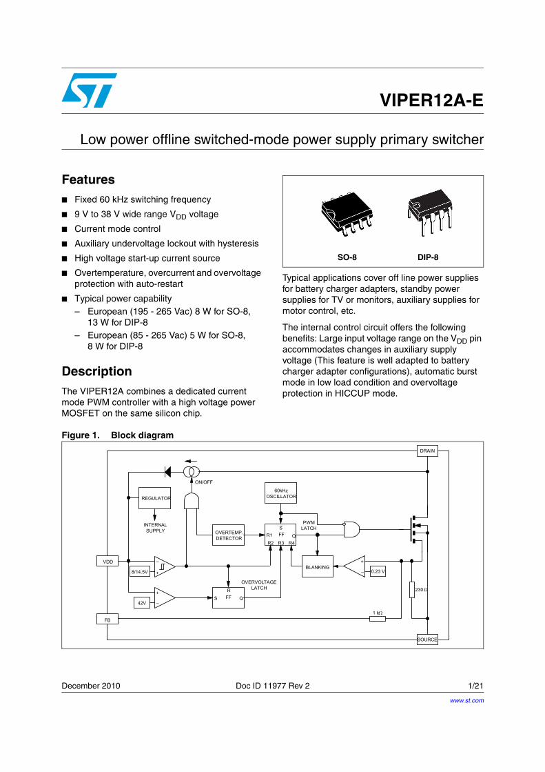
VIPER12A-E
Low power offline switched-mode power supply primary switcher
Features■ Fixed 60 kHz switching frequency
■ 9 V to 38 V wide range VDD voltage
■ Current mode control
■ Auxiliary undervoltage lockout with hysteresis
■ High voltage start-up current source
■ Overtemperature, overcurrent and overvoltage protection with auto-restart
■ Typical power capability– European (195 - 265 Vac) 8 W for SO-8,
13 W for DIP-8– European (85 - 265 Vac) 5 W for SO-8,
8 W for DIP-8
DescriptionThe VIPER12A combines a dedicated current mode PWM controller with a high voltage power MOSFET on the same silicon chip.
Typical applications cover off line power supplies for battery charger adapters, standby power supplies for TV or monitors, auxiliary supplies for motor control, etc.
The internal control circuit offers the following benefits: Large input voltage range on the VDD pin accommodates changes in auxiliary supply voltage (This feature is well adapted to battery charger adapter configurations), automatic burst mode in low load condition and overvoltage protection in HICCUP mode.
Figure 1. Block diagram
DIP-8SO-8
ON/OFF
0.23 V
DRAIN
SOURCE
VDD
PWMLATCH
60kHzOSCILLATOR
BLANKING+
_8/14.5V
_
+
FFS
R1R4
QR3
FB
REGULATOR
INTERNALSUPPLY
OVERVOLTAGELATCH
OVERTEMP.DETECTOR
1 kΩ
42V _
+
R2
FFS
R
Q
230 Ω
www.st.com
Contents VIPER12A-E
2/21 Doc ID 11977 Rev 2
Contents
1 Electrical data . . . . . . . . . . . . . . . . . . . . . . . . . . . . . . . . . . . . . . . . . . . . . . 3
1.1 Maximum rating . . . . . . . . . . . . . . . . . . . . . . . . . . . . . . . . . . . . . . . . . . . . . 3
1.2 Thermal data . . . . . . . . . . . . . . . . . . . . . . . . . . . . . . . . . . . . . . . . . . . . . . . 3
2 Electrical characteristics . . . . . . . . . . . . . . . . . . . . . . . . . . . . . . . . . . . . . 4
3 Pin connections and function . . . . . . . . . . . . . . . . . . . . . . . . . . . . . . . . . 6
4 Rectangular U-I output characteristics . . . . . . . . . . . . . . . . . . . . . . . . . . 7
5 Wide range of VDD voltage . . . . . . . . . . . . . . . . . . . . . . . . . . . . . . . . . . . 8
6 Feedback pin principle of operation . . . . . . . . . . . . . . . . . . . . . . . . . . . . 9
7 Startup sequence . . . . . . . . . . . . . . . . . . . . . . . . . . . . . . . . . . . . . . . . . . 11
8 Overvoltage threshold . . . . . . . . . . . . . . . . . . . . . . . . . . . . . . . . . . . . . . 12
9 Operation pictures . . . . . . . . . . . . . . . . . . . . . . . . . . . . . . . . . . . . . . . . . 13
10 Package mechanical data . . . . . . . . . . . . . . . . . . . . . . . . . . . . . . . . . . . . 16
11 Order codes . . . . . . . . . . . . . . . . . . . . . . . . . . . . . . . . . . . . . . . . . . . . . . . 19
12 Revision history . . . . . . . . . . . . . . . . . . . . . . . . . . . . . . . . . . . . . . . . . . . 20
VIPER12A-E Electrical data
Doc ID 11977 Rev 2 3/21
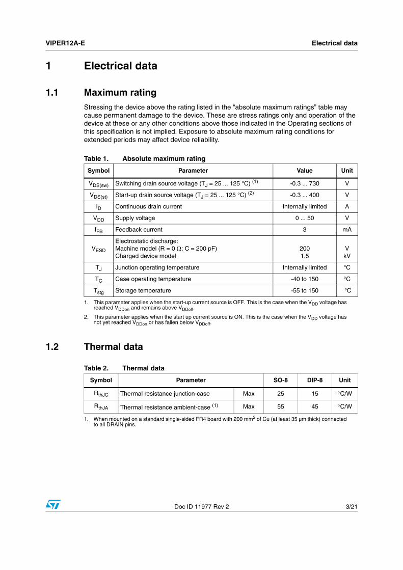
1 Electrical data
1.1 Maximum ratingStressing the device above the rating listed in the “absolute maximum ratings” table may cause permanent damage to the device. These are stress ratings only and operation of the device at these or any other conditions above those indicated in the Operating sections of this specification is not implied. Exposure to absolute maximum rating conditions for extended periods may affect device reliability.
1.2 Thermal data
Table 1. Absolute maximum rating
Symbol Parameter Value Unit
VDS(sw) Switching drain source voltage (TJ = 25 ... 125 °C) (1)
1. This parameter applies when the start-up current source is OFF. This is the case when the VDD voltage has reached VDDon and remains above VDDoff.
-0.3 ... 730 V
VDS(st) Start-up drain source voltage (TJ = 25 ... 125 °C) (2)
2. This parameter applies when the start up current source is ON. This is the case when the VDD voltage has not yet reached VDDon or has fallen below VDDoff.
-0.3 ... 400 V
ID Continuous drain current Internally limited A
VDD Supply voltage 0 ... 50 V
IFB Feedback current 3 mA
VESD Electrostatic discharge: Machine model (R = 0 Ω; C = 200 pF) Charged device model
2001.5
V kV
TJ Junction operating temperature Internally limited °C
TC Case operating temperature -40 to 150 °C
Tstg Storage temperature -55 to 150 °C
Table 2. Thermal data
Symbol Parameter SO-8 DIP-8 Unit
RthJC Thermal resistance junction-case Max 25 15 °C/W
RthJA Thermal resistance ambient-case (1)
1. When mounted on a standard single-sided FR4 board with 200 mm2 of Cu (at least 35 µm thick) connected to all DRAIN pins.
Max 55 45 °C/W
Electrical characteristics VIPER12A-E
4/21 Doc ID 11977 Rev 2
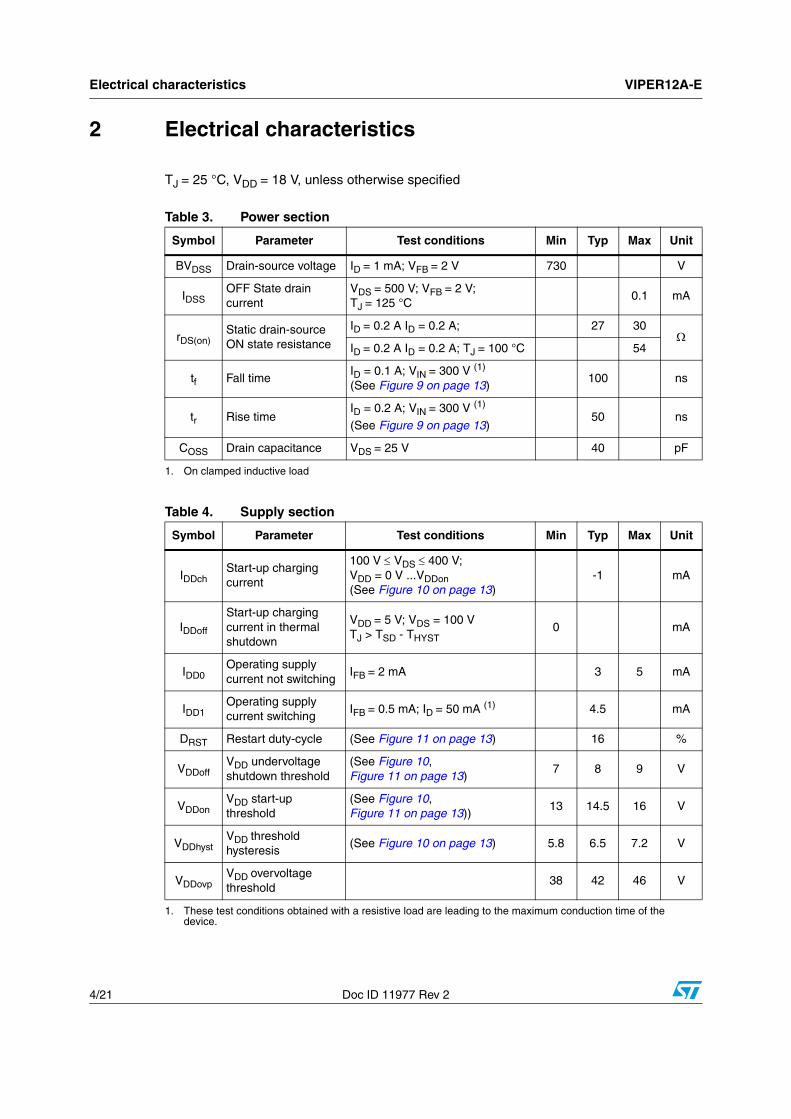
2 Electrical characteristics
TJ = 25 °C, VDD = 18 V, unless otherwise specified
Table 3. Power section
Symbol Parameter Test conditions Min Typ Max Unit
BVDSS Drain-source voltage ID = 1 mA; VFB = 2 V 730 V
IDSS OFF State drain current
VDS = 500 V; VFB = 2 V; TJ = 125 °C
0.1 mA
rDS(on) Static drain-source ON state resistance
ID = 0.2 A ID = 0.2 A; 27 30 Ω
ID = 0.2 A ID = 0.2 A; TJ = 100 °C 54
tf Fall time ID = 0.1 A; VIN = 300 V (1) (See Figure 9 on page 13)
1. On clamped inductive load
100 ns
tr Rise time ID = 0.2 A; VIN = 300 V (1)
(See Figure 9 on page 13) 50 ns
COSS Drain capacitance VDS = 25 V 40 pF
Table 4. Supply section
Symbol Parameter Test conditions Min Typ Max Unit
IDDch Start-up charging current
100 V ≤ VDS ≤ 400 V;VDD = 0 V ...VDDon (See Figure 10 on page 13)
-1 mA
IDDoff Start-up charging current in thermal shutdown
VDD = 5 V; VDS = 100 V TJ > TSD - THYST
0 mA
IDD0 Operating supply current not switching
IFB = 2 mA 3 5 mA
IDD1 Operating supply current switching
IFB = 0.5 mA; ID = 50 mA (1)
1. These test conditions obtained with a resistive load are leading to the maximum conduction time of the device.
4.5 mA
DRST Restart duty-cycle (See Figure 11 on page 13) 16 %
VDDoff VDD undervoltage shutdown threshold
(See Figure 10, Figure 11 on page 13)
7 8 9 V
VDDon VDD start-up threshold
(See Figure 10, Figure 11 on page 13))
13 14.5 16 V
VDDhyst VDD threshold hysteresis
(See Figure 10 on page 13) 5.8 6.5 7.2 V
VDDovp VDD overvoltage threshold
38 42 46 V
VIPER12A-E Electrical characteristics
Doc ID 11977 Rev 2 5/21
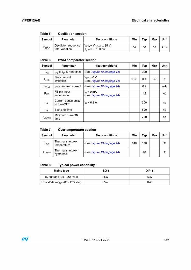
Table 5. Oscillation section
Symbol Parameter Test conditions Min Typ Max Unit
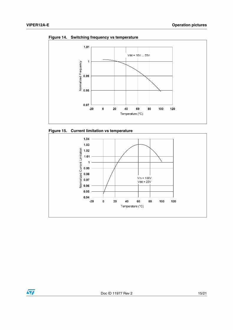
FOSC Oscillator frequency total variation
VDD = VDDoff ... 35 V; TJ = 0 ... 100 °C
54 60 66 kHz
Table 6. PWM comparator section
Symbol Parameter Test conditions Min Typ Max Unit
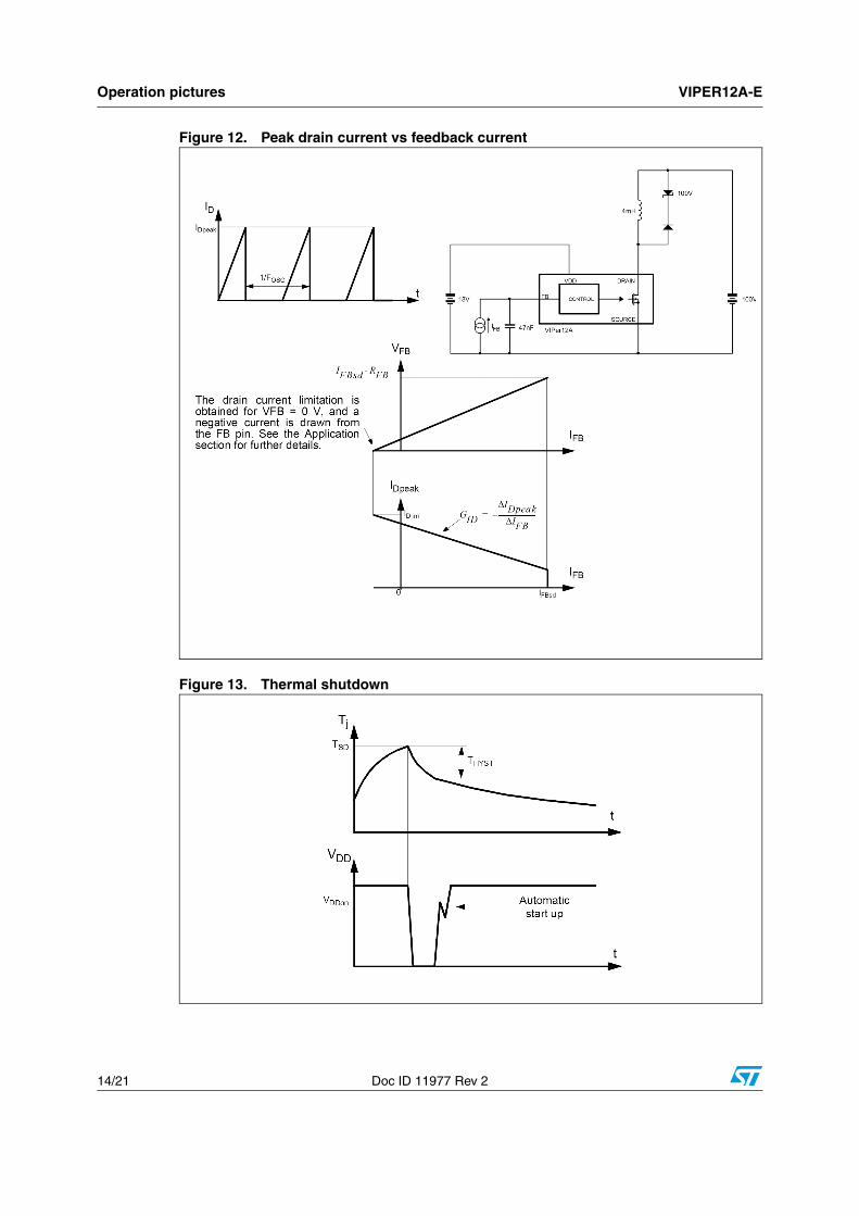
GID IFB to ID current gain (See Figure 12 on page 14) 320
IDlim Peak current limitation
VFB = 0 V (See Figure 12 on page 14)
0.32 0.4 0.48 A
IFBsd IFB shutdown current (See Figure 12 on page 14) 0.9 mA
RFB FB pin input impedance
ID = 0 mA (See Figure 12 on page 14)
1.2 kΩ
td Current sense delay to turn-OFF
ID = 0.2 A 200 ns
tb Blanking time 500 ns
tONminMinimum Turn-ON time
700 ns
Table 7. Overtemperature section
Symbol Parameter Test conditions Min Typ Max Unit
TSD Thermal shutdown temperature
(See Figure 13 on page 14) 140 170 °C
THYST Thermal shutdown hysteresis
(See Figure 13 on page 14) 40 °C
Table 8. Typical power capability
Mains type SO-8 DIP-8
European (195 - 265 Vac) 8W 13W
US / Wide range (85 - 265 Vac) 5W 8W
Pin connections and function VIPER12A-E
6/21 Doc ID 11977 Rev 2
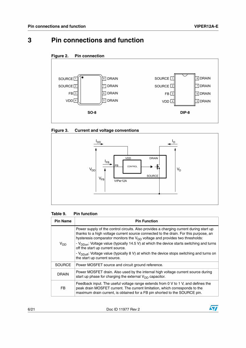
3 Pin connections and function
Figure 2. Pin connection
Figure 3. Current and voltage conventions
Table 9. Pin function
Pin Name Pin Function
VDD
Power supply of the control circuits. Also provides a charging current during start up thanks to a high voltage current source connected to the drain. For this purpose, an hysteresis comparator monitors the VDD voltage and provides two thresholds:
- VDDon: Voltage value (typically 14.5 V) at which the device starts switching and turns off the start up current source.
- VDDoff: Voltage value (typically 8 V) at which the device stops switching and turns on the start up current source.
SOURCE Power MOSFET source and circuit ground reference.
DRAINPower MOSFET drain. Also used by the internal high voltage current source during start up phase for charging the external VDD capacitor.
FBFeedback input. The useful voltage range extends from 0 V to 1 V, and defines the peak drain MOSFET current. The current limitation, which corresponds to the maximum drain current, is obtained for a FB pin shorted to the SOURCE pin.
1
2
3
4
DRAIN
DRAIN
DRAIN
DRAIN
8
7
6
5
DRAIN
DRAIN
DRAIN
DRAIN
1
2
3
4
8
7
6
5
FB
VDD
SOURCE
FB
VDD
SOURCE
SOURCE SOURCE
SO-8 DIP-8
IDD ID
IFB
VDD
VFB
VD
FB
VDD DRAIN
SOURCE
CONTROL
VIPer12A
VIPER12A-E Rectangular U-I output characteristics
Doc ID 11977 Rev 2 7/21
4 Rectangular U-I output characteristics
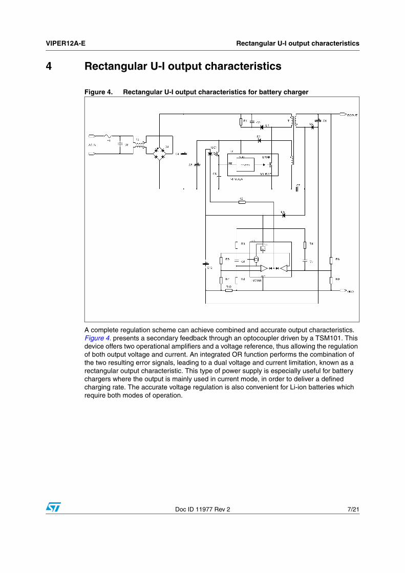
Figure 4. Rectangular U-I output characteristics for battery charger
A complete regulation scheme can achieve combined and accurate output characteristics. Figure 4. presents a secondary feedback through an optocoupler driven by a TSM101. This device offers two operational amplifiers and a voltage reference, thus allowing the regulation of both output voltage and current. An integrated OR function performs the combination of the two resulting error signals, leading to a dual voltage and current limitation, known as a rectangular output characteristic. This type of power supply is especially useful for battery chargers where the output is mainly used in current mode, in order to deliver a defined charging rate. The accurate voltage regulation is also convenient for Li-ion batteries which require both modes of operation.
Wide range of VDD voltage VIPER12A-E
8/21 Doc ID 11977 Rev 2
5 Wide range of VDD voltage
The VDD pin voltage range extends from 9 V to 38 V. This feature offers a great flexibility in design to achieve various behaviors. In Figure 4 on page 7 a forward configuration has been chosen to supply the device with two benefits:
● As soon as the device starts switching, it immediately receives some energy from the auxiliary winding. C5 can be therefore reduced and a small ceramic chip (100 nF) is sufficient to insure the filtering function. The total start up time from the switch on of input voltage to output voltage presence is dramatically decreased.
● The output current characteristic can be maintained even with very low or zero output voltage. Since the TSM101 is also supplied in forward mode, it keeps the current regulation up whatever the output voltage is.The VDD pin voltage may vary as much as the input voltage, that is to say with a ratio of about 4 for a wide range application.
VIPER12A-E Feedback pin principle of operation
Doc ID 11977 Rev 2 9/21
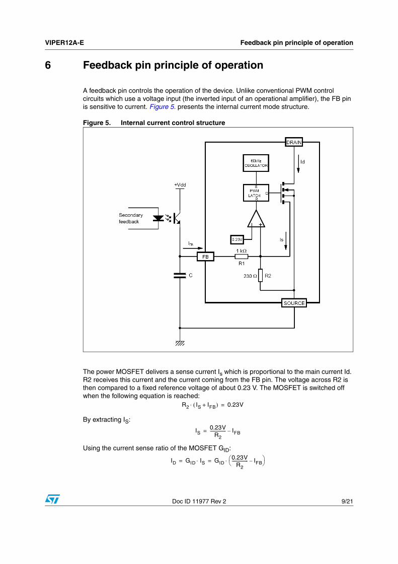
6 Feedback pin principle of operation
A feedback pin controls the operation of the device. Unlike conventional PWM control circuits which use a voltage input (the inverted input of an operational amplifier), the FB pin is sensitive to current. Figure 5. presents the internal current mode structure.
Figure 5. Internal current control structure
The power MOSFET delivers a sense current Is which is proportional to the main current Id. R2 receives this current and the current coming from the FB pin. The voltage across R2 is then compared to a fixed reference voltage of about 0.23 V. The MOSFET is switched off when the following equation is reached:
By extracting IS:
Using the current sense ratio of the MOSFET GID:
R2 IS IFB+( )⋅ 0.23V=
IS0.23V
R2---------------- IFB–=
ID GID IS⋅ GID0.23V
R2---------------- IFB–⎝ ⎠
⎛ ⎞⋅= =
Feedback pin principle of operation VIPER12A-E
10/21 Doc ID 11977 Rev 2
The current limitation is obtained with the FB pin shorted to ground (VFB = 0 V). This leads to a negative current sourced by this pin, and expressed by:
By reporting this expression in the previous one, it is possible to obtain the drain current limitation IDlim:
In a real application, the FB pin is driven with an optocoupler as shown on Figure 5 which acts as a pull up. So, it is not possible to really short this pin to ground and the above drain current value is not achievable. Nevertheless, the capacitor C is averaging the voltage on the FB pin, and when the optocoupler is off (start up or short circuit), it can be assumed that the corresponding voltage is very close to 0 V.
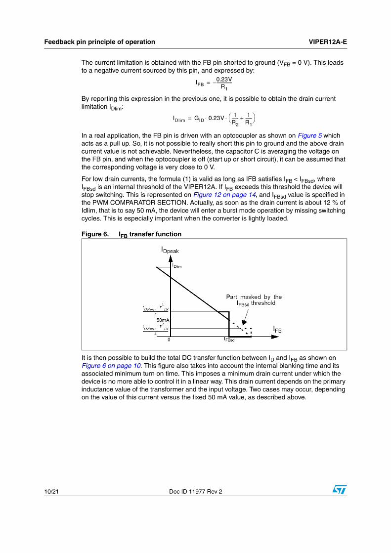
For low drain currents, the formula (1) is valid as long as IFB satisfies IFB < IFBsd, where IFBsd is an internal threshold of the VIPER12A. If IFB exceeds this threshold the device will stop switching. This is represented on Figure 12 on page 14, and IFBsd value is specified in the PWM COMPARATOR SECTION. Actually, as soon as the drain current is about 12 % of Idlim, that is to say 50 mA, the device will enter a burst mode operation by missing switching cycles. This is especially important when the converter is lightly loaded.
Figure 6. IFB transfer function
It is then possible to build the total DC transfer function between ID and IFB as shown on Figure 6 on page 10. This figure also takes into account the internal blanking time and its associated minimum turn on time. This imposes a minimum drain current under which the device is no more able to control it in a linear way. This drain current depends on the primary inductance value of the transformer and the input voltage. Two cases may occur, depending on the value of this current versus the fixed 50 mA value, as described above.
IFB0.23V
R1----------------–=
IDlim GID 0.23V 1R2------- 1
R1-------+⎝ ⎠
⎛ ⎞⋅ ⋅=
VIPER12A-E Startup sequence
Doc ID 11977 Rev 2 11/21
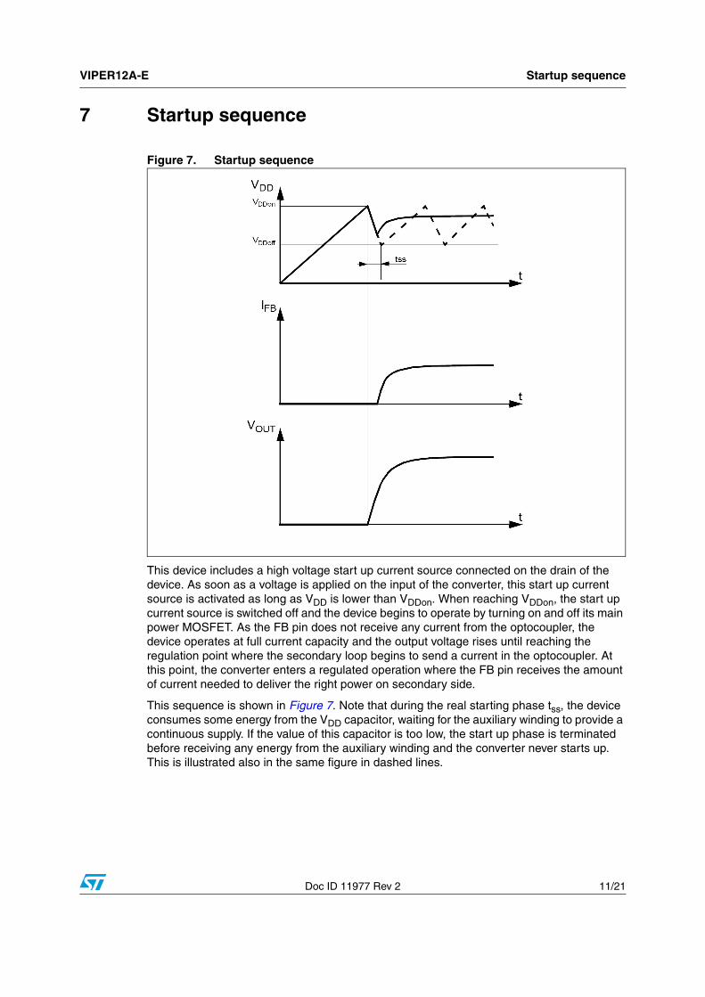
7 Startup sequence
Figure 7. Startup sequence
This device includes a high voltage start up current source connected on the drain of the device. As soon as a voltage is applied on the input of the converter, this start up current source is activated as long as VDD is lower than VDDon. When reaching VDDon, the start up current source is switched off and the device begins to operate by turning on and off its main power MOSFET. As the FB pin does not receive any current from the optocoupler, the device operates at full current capacity and the output voltage rises until reaching the regulation point where the secondary loop begins to send a current in the optocoupler. At this point, the converter enters a regulated operation where the FB pin receives the amount of current needed to deliver the right power on secondary side.
This sequence is shown in Figure 7. Note that during the real starting phase tss, the device consumes some energy from the VDD capacitor, waiting for the auxiliary winding to provide a continuous supply. If the value of this capacitor is too low, the start up phase is terminated before receiving any energy from the auxiliary winding and the converter never starts up. This is illustrated also in the same figure in dashed lines.
Overvoltage threshold VIPER12A-E
12/21 Doc ID 11977 Rev 2
8 Overvoltage threshold
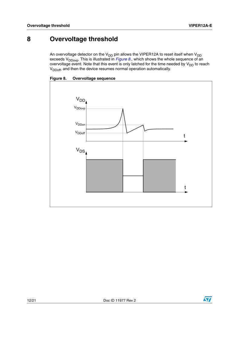
An overvoltage detector on the VDD pin allows the VIPER12A to reset itself when VDD exceeds VDDovp. This is illustrated in Figure 8., which shows the whole sequence of an overvoltage event. Note that this event is only latched for the time needed by VDD to reach VDDoff, and then the device resumes normal operation automatically.
Figure 8. Overvoltage sequence
t
t
VDS
VDDon
VDD
VDDoff
VDDovp
VIPER12A-E Operation pictures
Doc ID 11977 Rev 2 13/21
9 Operation pictures
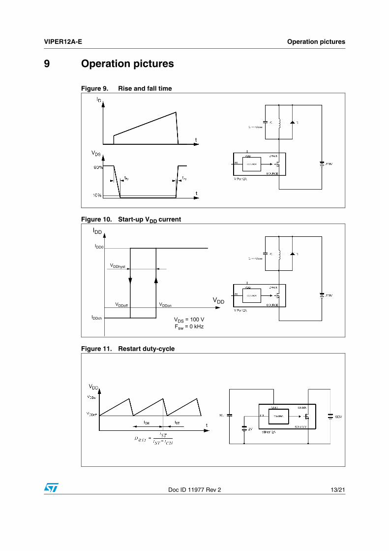
Figure 9. Rise and fall time
Figure 10. Start-up VDD current
Figure 11. Restart duty-cycle
VDD
VDDhyst
VDDoff VDDon
IDD0
IDDch VDS = 100 VFsw = 0 kHz
IDD
Operation pictures VIPER12A-E
14/21 Doc ID 11977 Rev 2
Figure 12. Peak drain current vs feedback current
Figure 13. Thermal shutdown
VIPER12A-E Operation pictures
Doc ID 11977 Rev 2 15/21
Figure 14. Switching frequency vs temperature
Figure 15. Current limitation vs temperature
Package mechanical data VIPER12A-E
16/21 Doc ID 11977 Rev 2
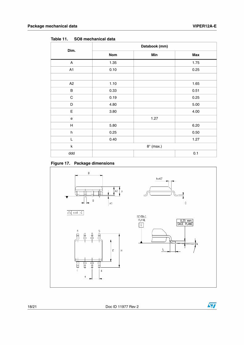
10 Package mechanical data
In order to meet environmental requirements, ST offers these devices in different grades of ECOPACK® packages, depending on their level of environmental compliance. ECOPACK® specifications, grade definitions and product status are available at: www.st.com. ECOPACK is an ST trademark.
VIPER12A-E Package mechanical data
Doc ID 11977 Rev 2 17/21
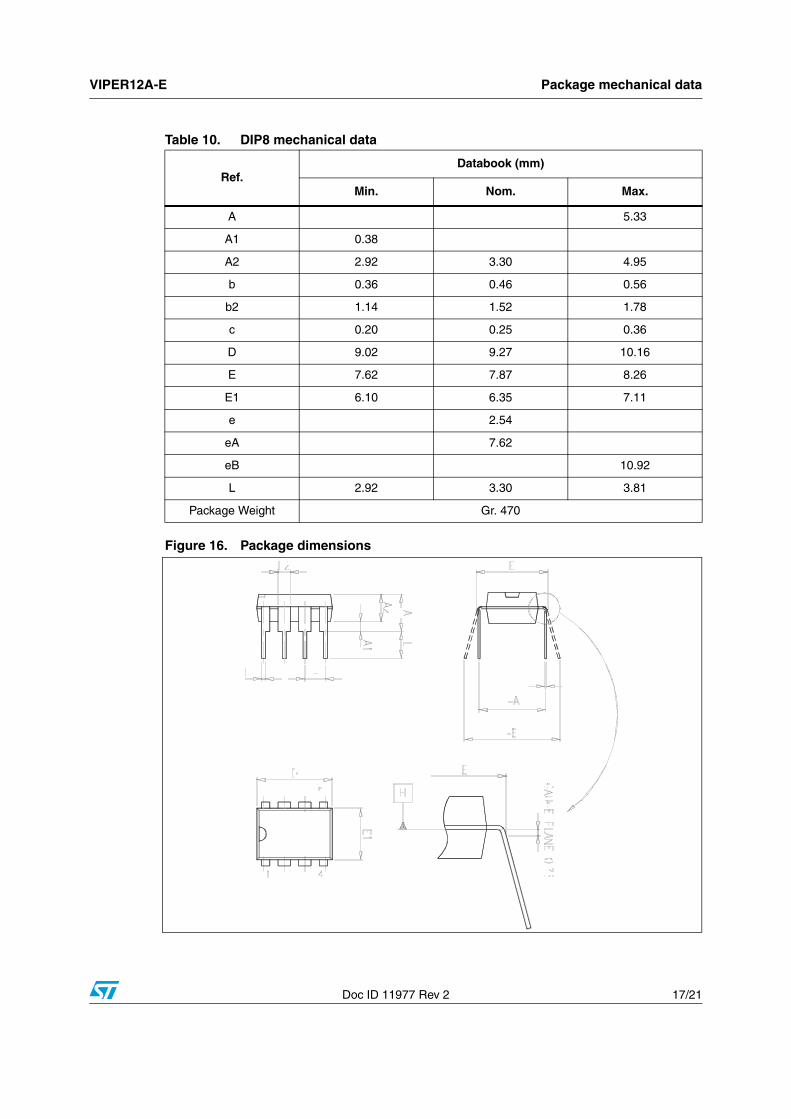
Figure 16. Package dimensions
Table 10. DIP8 mechanical data
Ref.Databook (mm)
Min. Nom. Max.
A 5.33
A1 0.38
A2 2.92 3.30 4.95
b 0.36 0.46 0.56
b2 1.14 1.52 1.78
c 0.20 0.25 0.36
D 9.02 9.27 10.16
E 7.62 7.87 8.26
E1 6.10 6.35 7.11
e 2.54
eA 7.62
eB 10.92
L 2.92 3.30 3.81
Package Weight Gr. 470
Package mechanical data VIPER12A-E
18/21 Doc ID 11977 Rev 2
Figure 17. Package dimensions
Table 11. SO8 mechanical data
Dim.Databook (mm)
Nom Min Max
A 1.35 1.75
A1 0.10 0.25
A2 1.10 1.65
B 0.33 0.51
C 0.19 0.25
D 4.80 5.00
E 3.80 4.00
e 1.27
H 5.80 6.20
h 0.25 0.50
L 0.40 1.27
k 8° (max.)
ddd 0.1
VIPER12A-E Order codes
Doc ID 11977 Rev 2 19/21
11 Order codes
Table 12. Order codes
Order codes Package Packaging
VIPER12ASTR-E SO-8 Tape and reel
VIPER12AS-E SO-8 Tube
VIPER12ADIP-E DIP-8 Tube
Revision history VIPER12A-E
20/21 Doc ID 11977 Rev 2
12 Revision history
Table 13. Document revision history
Date Revision Changes
09-Jan-2006 1 Initial release.
13-Dec-2010 2Updated Table 3 on page 4, Table 4 on page 4 and Figure 10 on page 13.
VIPER12A-E
Doc ID 11977 Rev 2 21/21
Please Read Carefully:
Information in this document is provided solely in connection with ST products. STMicroelectronics NV and its subsidiaries (“ST”) reserve theright to make changes, corrections, modifications or improvements, to this document, and the products and services described herein at anytime, without notice.
All ST products are sold pursuant to ST’s terms and conditions of sale.
Purchasers are solely responsible for the choice, selection and use of the ST products and services described herein, and ST assumes noliability whatsoever relating to the choice, selection or use of the ST products and services described herein.
No license, express or implied, by estoppel or otherwise, to any intellectual property rights is granted under this document. If any part of thisdocument refers to any third party products or services it shall not be deemed a license grant by ST for the use of such third party productsor services, or any intellectual property contained therein or considered as a warranty covering the use in any manner whatsoever of suchthird party products or services or any intellectual property contained therein.
UNLESS OTHERWISE SET FORTH IN ST’S TERMS AND CONDITIONS OF SALE ST DISCLAIMS ANY EXPRESS OR IMPLIEDWARRANTY WITH RESPECT TO THE USE AND/OR SALE OF ST PRODUCTS INCLUDING WITHOUT LIMITATION IMPLIEDWARRANTIES OF MERCHANTABILITY, FITNESS FOR A PARTICULAR PURPOSE (AND THEIR EQUIVALENTS UNDER THE LAWSOF ANY JURISDICTION), OR INFRINGEMENT OF ANY PATENT, COPYRIGHT OR OTHER INTELLECTUAL PROPERTY RIGHT.
UNLESS EXPRESSLY APPROVED IN WRITING BY AN AUTHORIZED ST REPRESENTATIVE, ST PRODUCTS ARE NOTRECOMMENDED, AUTHORIZED OR WARRANTED FOR USE IN MILITARY, AIR CRAFT, SPACE, LIFE SAVING, OR LIFE SUSTAININGAPPLICATIONS, NOR IN PRODUCTS OR SYSTEMS WHERE FAILURE OR MALFUNCTION MAY RESULT IN PERSONAL INJURY,DEATH, OR SEVERE PROPERTY OR ENVIRONMENTAL DAMAGE. ST PRODUCTS WHICH ARE NOT SPECIFIED AS "AUTOMOTIVEGRADE" MAY ONLY BE USED IN AUTOMOTIVE APPLICATIONS AT USER’S OWN RISK.
Resale of ST products with provisions different from the statements and/or technical features set forth in this document shall immediately voidany warranty granted by ST for the ST product or service described herein and shall not create or extend in any manner whatsoever, anyliability of ST.
ST and the ST logo are trademarks or registered trademarks of ST in various countries.
Information in this document supersedes and replaces all information previously supplied.
The ST logo is a registered trademark of STMicroelectronics. All other names are the property of their respective owners.
© 2010 STMicroelectronics - All rights reserved
STMicroelectronics group of companies
Australia - Belgium - Brazil - Canada - China - Czech Republic - Finland - France - Germany - Hong Kong - India - Israel - Italy - Japan - Malaysia - Malta - Morocco - Philippines - Singapore - Spain - Sweden - Switzerland - United Kingdom - United States of America
www.st.com