Embed Size (px)
Citation preview
1
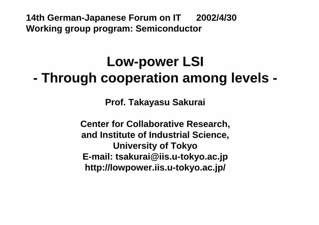
Low-power LSI- Through cooperation among levels -
Prof. Takayasu Sakurai
Center for Collaborative Research,and Institute of Industrial Science,
University of TokyoE-mail: [email protected]://lowpower.iis.u-tokyo.ac.jp/
1
14th German-Japanese Forum on IT 2002/4/30Working group program: Semiconductor
T.SakuraiT.Sakurai
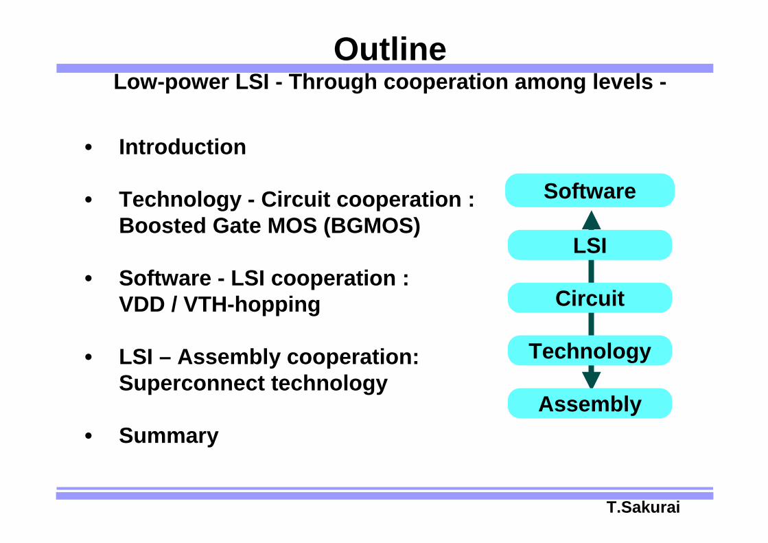
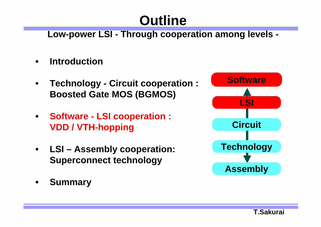
OutlineLow-power LSI - Through cooperation among levels -
Software
Circuit
Technology
Assembly
LSI
• Introduction
• Technology - Circuit cooperation : Boosted Gate MOS (BGMOS)
• Software - LSI cooperation : VDD / VTH-hopping
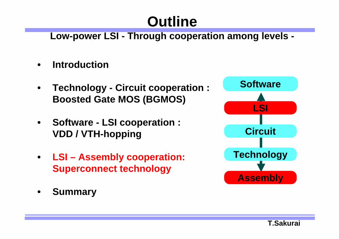
• LSI – Assembly cooperation:Superconnect technology
• Summary
T.SakuraiT.Sakurai
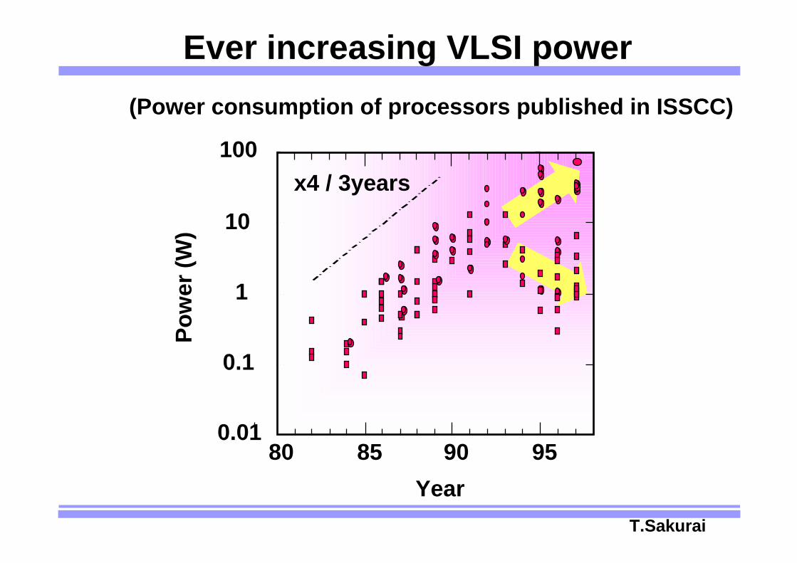
Ever increasing VLSI power(Power consumption of processors published in ISSCC)
959085800.01
0.1
1
10
100
Year
Pow
er (W
)x4 / 3years
T.SakuraiT.Sakurai
Year
Volta
ge [V
]
Pow
er p
er c
hip
[W]
VDD
cur
rent
[A]
VDD, power and current trend
1998 2002 2006 2010 20140
0.5
1
1.5
2
2.5
0 0
200 500
Current
Power
Voltage
International Technology Roadmap for Semiconductors 1999 update sponsored by the Semiconductor Industry Association in cooperation with European Electronic Component Association (EECA) , Electronic Industries Association of Japan (EIAJ), Korea Semiconductor Industry Association (KSIA), and Taiwan Semiconductor Industry Association (TSIA)
T.SakuraiT.Sakurai
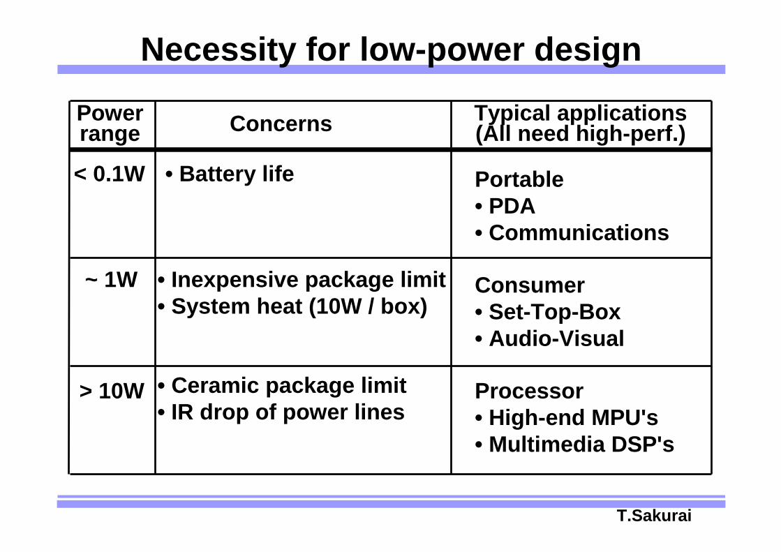
Necessity for low-power design
Power range Concerns
< 0.1W • Battery life Portable• PDA• Communications
~ 1W Consumer• Set-Top-Box• Audio-Visual
• Inexpensive package limit • System heat (10W / box)
> 10W • Ceramic package limit• IR drop of power lines
Processor• High-end MPU's• Multimedia DSP's
Typical applications (All need high-perf.)
T.SakuraiT.Sakurai
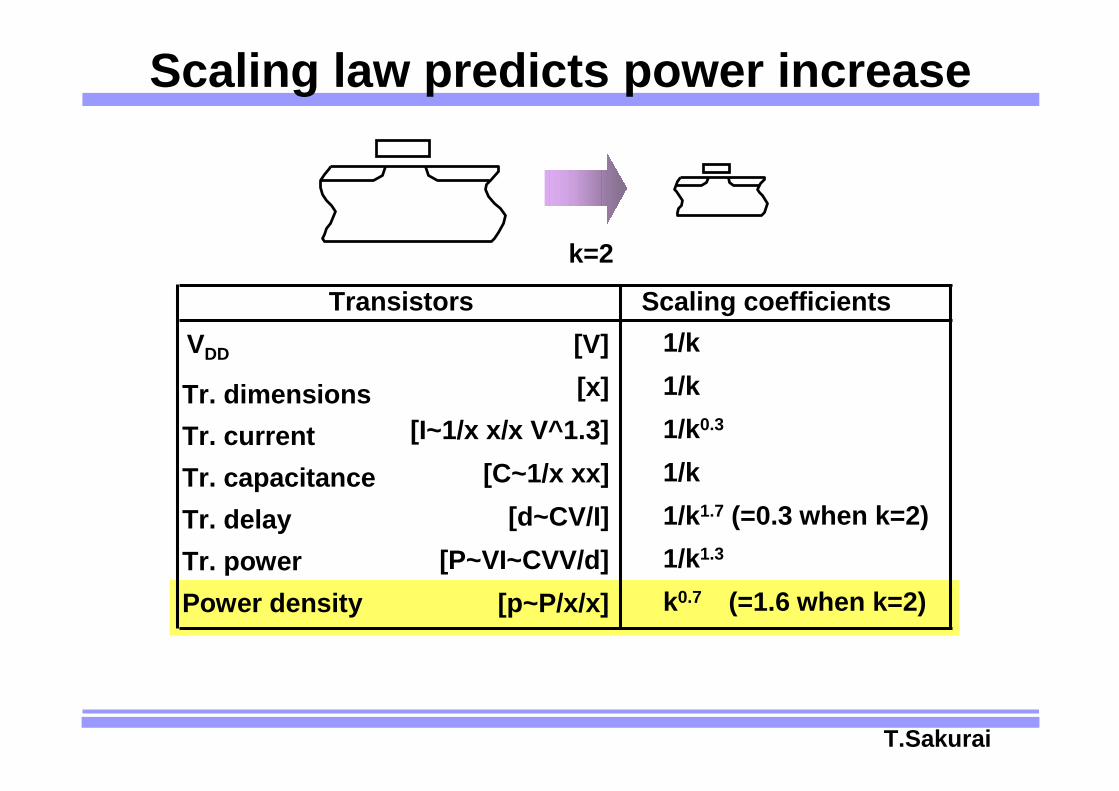
Scaling law predicts power increase
k=2
VDD [V] 1/k
Tr. dimensions [x] 1/k
Tr. current [I~1/x x/x V^1.3] 1/k0.3
Tr. capacitance [C~1/x xx] 1/kTr. delay [d~CV/I] 1/k1.7 (=0.3 when k=2)Tr. power [P~VI~CVV/d] 1/k1.3
Power density [p~P/x/x] k0.7 (=1.6 when k=2)
Transistors Scaling coefficients
T.SakuraiT.Sakurai
Power & delay dependence on VDD & VTH
Power : P = pt •fCLK •CL •VDD + I0 •10 •VDD 2
V thS
(αααα=1.3)
k • CL • VDD
(VDD - Vth)ααααDelay =
k•QI
=
12
34
-0.400.40.8
00.2
0.4
0.6
0.8
1x 10⁻⁴
Vth (V)
VDD(V)
Pow
er (W
)
A
B
12
34
-0.400.40.8
0
1
2
3
4
5x 10
-10
Del
ay (s
)
Vth (V)VDD(V)
A B
T.SakuraiT.Sakurai
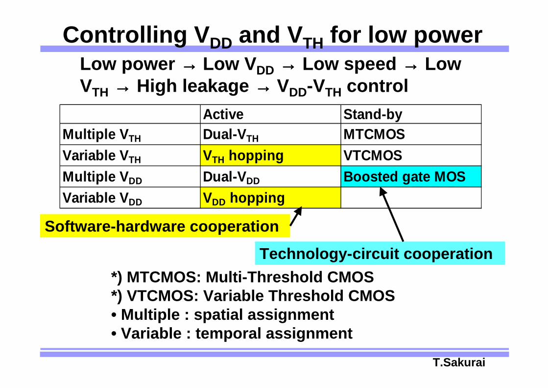
Controlling VDD and VTH for low powerLow power →→→→ Low VDD →→→→ Low speed →→→→ Low VTH →→→→ High leakage →→→→ VDD-VTH control
Active Stand-byMultiple VTH Dual-VTH MTCMOSVariable VTH VTH hopping VTCMOSMultiple VDD Dual-VDD Boosted gate MOSVariable VDD VDD hopping
*) MTCMOS: Multi-Threshold CMOS*) VTCMOS: Variable Threshold CMOS• Multiple : spatial assignment• Variable : temporal assignment
Software-hardware cooperationTechnology-circuit cooperation
T.SakuraiT.Sakurai
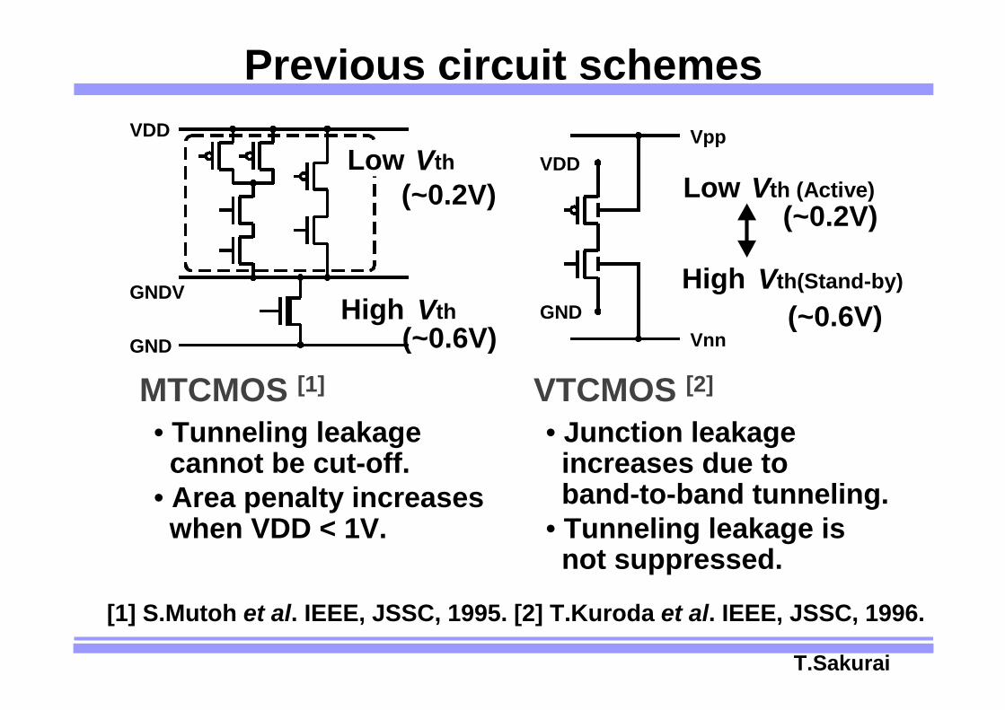
Previous circuit schemes
[1] S.Mutoh et al. IEEE, JSSC, 1995. [2] T.Kuroda et al. IEEE, JSSC, 1996.
MTCMOS [1] VTCMOS [2]
• Tunneling leakagecannot be cut-off.
• Area penalty increaseswhen VDD < 1V.
• Junction leakage increases due toband-to-band tunneling.
• Tunneling leakage isnot suppressed.
High Vth(Stand-by)
Low Vth (Active)VDD
Vnn
Vpp
GND
VDD
GNDV
GNDHigh Vth
Low Vth
(~0.6V)
(~0.2V) (~0.2V)
(~0.6V)
T.SakuraiT.Sakurai
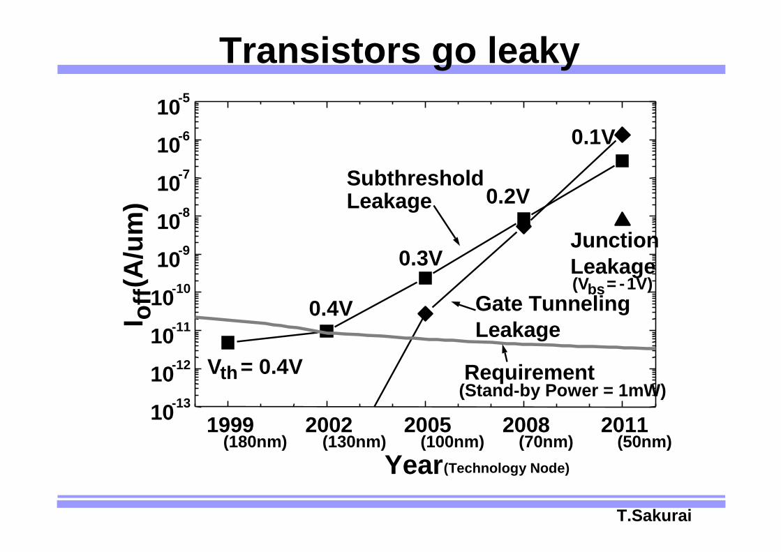
Transistors go leaky
1999 2002 2005 2008 201110-13
10-12
10-11
10-10
10-9
10-8
10-7
10-6
10-5
Requirement(Stand-by Power = 1mW)
(Vbs= -1V)
JunctionLeakage
0.1V
0.2V
0.3V
0.4V
Vth= 0.4V
SubthresholdLeakage
Gate TunnelingLeakage
(180nm) (50nm)(70nm)(100nm)(130nm)
I off
(A/u
m)
Year (Technology Node)
T.SakuraiT.Sakurai
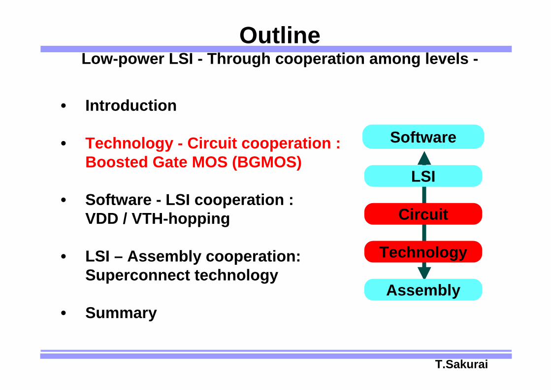
OutlineLow-power LSI - Through cooperation among levels -
Software
Circuit
Technology
Assembly
LSI
• Introduction
• Technology - Circuit cooperation : Boosted Gate MOS (BGMOS)
• Software - LSI cooperation : VDD / VTH-hopping
• LSI – Assembly cooperation:Superconnect technology
• Summary
T.SakuraiT.Sakurai
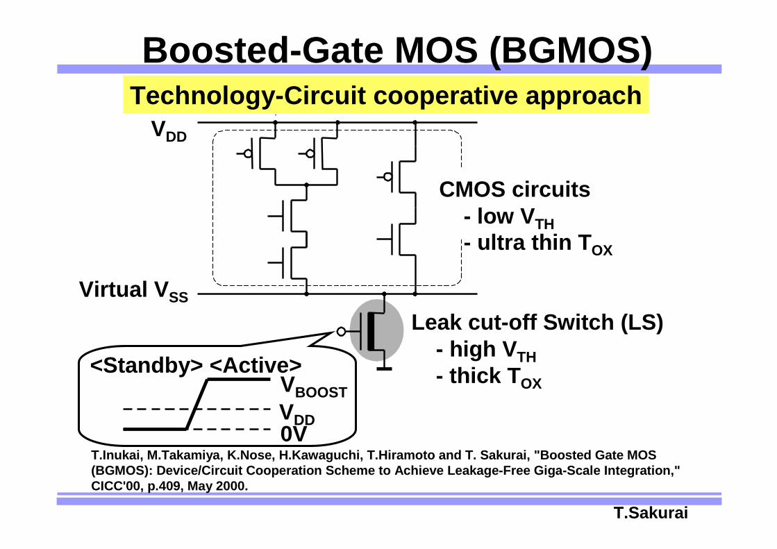
Boosted-Gate MOS (BGMOS)
Leak cut-off Switch (LS)- high VTH- thick TOX
VDD
Virtual VSS
CMOS circuits- low VTH- ultra thin TOX
T.Inukai, M.Takamiya, K.Nose, H.Kawaguchi, T.Hiramoto and T. Sakurai, "Boosted Gate MOS (BGMOS): Device/Circuit Cooperation Scheme to Achieve Leakage-Free Giga-Scale Integration," CICC'00, p.409, May 2000.
0VVDD
VBOOST<Standby> <Active>
Technology-Circuit cooperative approach
T.SakuraiT.Sakurai
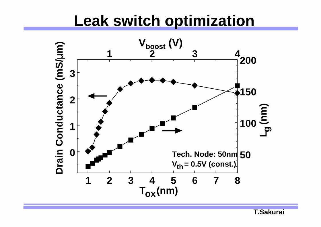
Leak switch optimization
1 2 3 4 5 6 7 8
0
1
2
3
Vth = 0.5V (const.)Tech. Node: 50nm
Tox(nm)
Dra
in C
ondu
ctan
ce (m
S/µµ µµm
)1 2 3 4
Vboost (V)
50
100
150
200
L g(n
m)
T.SakuraiT.Sakurai
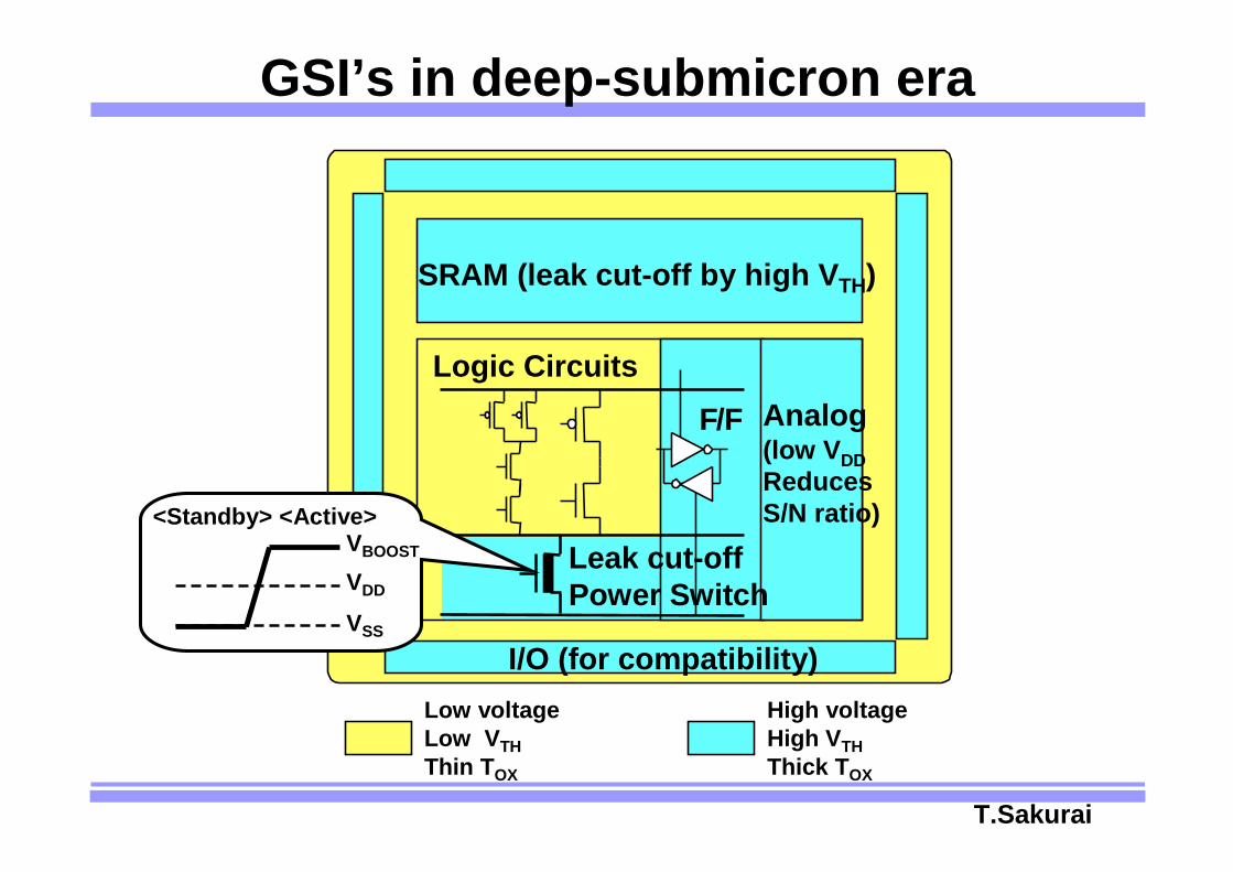
GSI’s in deep-submicron era
High voltageHigh VTHThick TOX
Low voltage Low VTHThin TOX
Logic CircuitsF/F
SRAM (leak cut-off by high VTH)
Leak cut-offPower Switch
Analog(low VDDReducesS/N ratio)
I/O (for compatibility)
VDD
VBOOST
<Standby> <Active>
VSS
T.SakuraiT.Sakurai
OutlineLow-power LSI - Through cooperation among levels -
Software
Circuit
Technology
Assembly
LSI
• Introduction
• Technology - Circuit cooperation : Boosted Gate MOS (BGMOS)
• Software - LSI cooperation : VDD / VTH-hopping
• LSI – Assembly cooperation:Superconnect technology
• Summary
T.SakuraiT.Sakurai
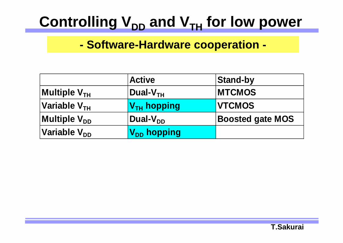
Controlling VDD and VTH for low power
Active Stand-byMultiple VTH Dual-VTH MTCMOSVariable VTH VTH hopping VTCMOSMultiple VDD Dual-VDD Boosted gate MOSVariable VDD VDD hopping
- Software-Hardware cooperation -
T.SakuraiT.Sakurai
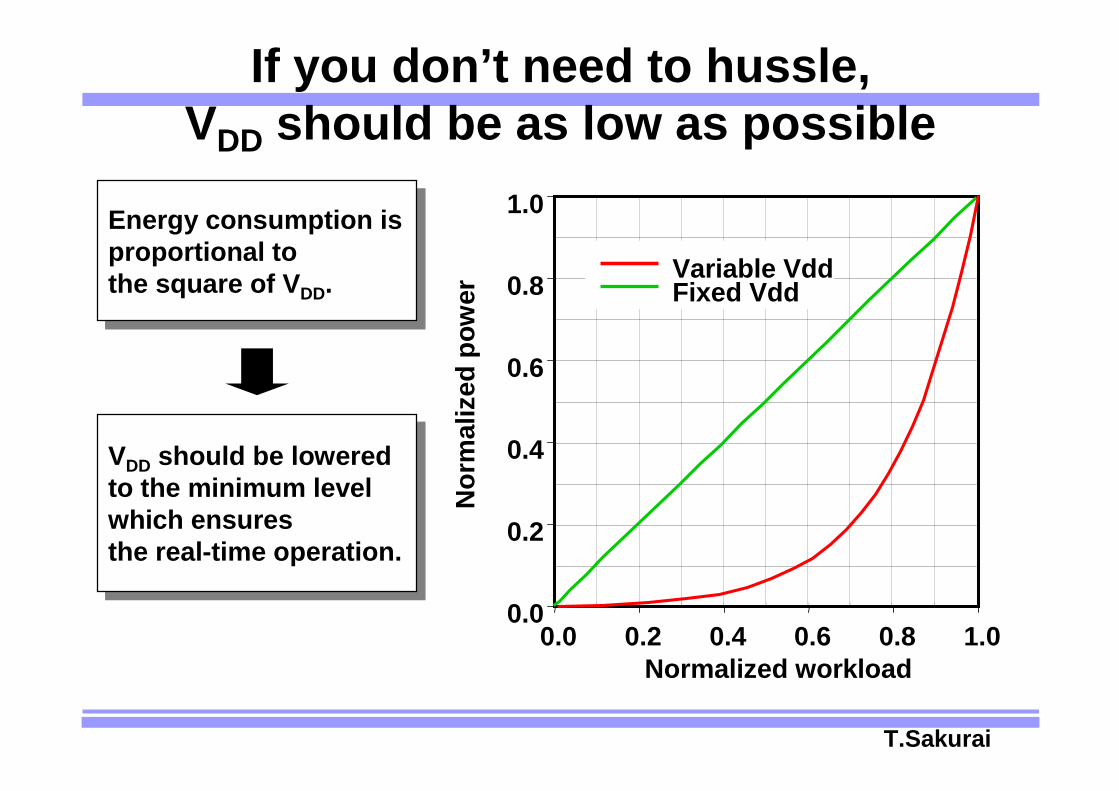
Energy consumption isproportional tothe square of VDD.
Energy consumption isproportional tothe square of VDD.
VDD should be loweredto the minimum levelwhich ensuresthe real-time operation.
VDD should be loweredto the minimum levelwhich ensuresthe real-time operation.
Normalized workload0.0 0.2 0.4 0.6 0.8 1.0
Nor
mal
ized
pow
er
0.0
0.2
0.4
0.6
0.8
1.0
Variable VddFixed Vdd
If you don’t need to hussle,VDD should be as low as possible
T.SakuraiT.Sakurai
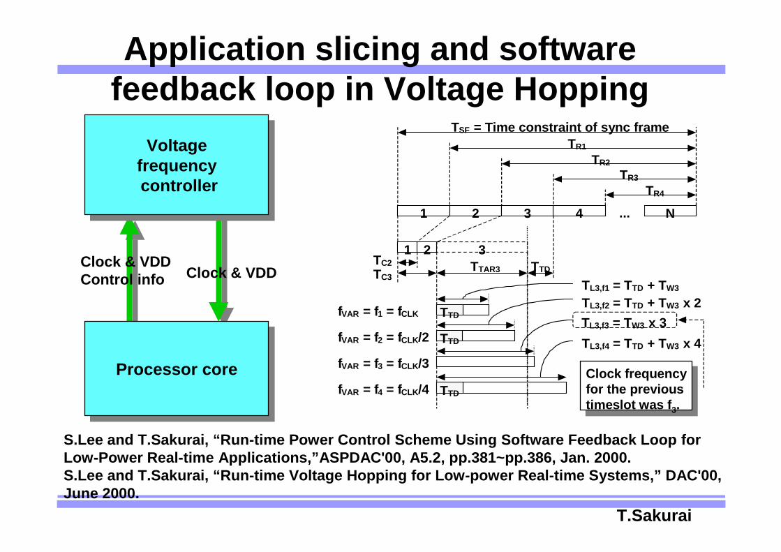
Application slicing and software feedback loop in Voltage Hopping
S.Lee and T.Sakurai, “Run-time Power Control Scheme Using Software Feedback Loop for Low-Power Real-time Applications,”ASPDAC'00, A5.2, pp.381~pp.386, Jan. 2000.S.Lee and T.Sakurai, “Run-time Voltage Hopping for Low-power Real-time Systems,” DAC'00, June 2000.
3
1 2 3 N...4
TR3
TR1TR2
TR4
TSF = Time constraint of sync frame
1 2TC2TC3
TTAR3
fVAR = f1 = fCLK TTD
TTD
fVAR = f2 = fCLK/2
fVAR = f3 = fCLK/3
fVAR = f4 = fCLK/4
TTD
TTD
TL3,f1 = TTD + TW3
TL3,f2 = TTD + TW3 x 2
TL3,f4 = TTD + TW3 x 4TL3,f3 = TW3 x 3
Clock frequency for the previous timeslot was f3.
Processor coreProcessor core
Voltagefrequencycontroller
Voltagefrequencycontroller
Clock & VDDClock & VDDControl info
T.SakuraiT.Sakurai
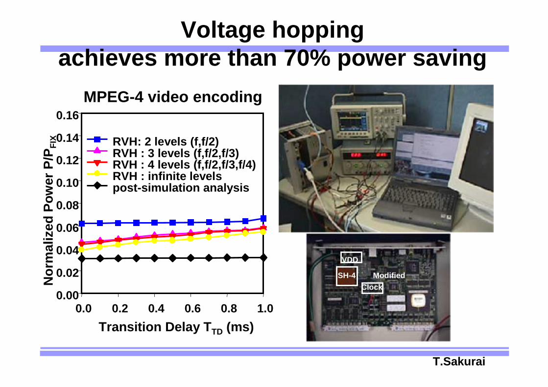
Voltage hoppingachieves more than 70% power saving
MPEG-4 video encoding
Transition Delay TTD (ms)0.0 0.2 0.4 0.6 0.8 1.0
Nor
mal
ized
Pow
er P
/PFI
X
0.00
0.02
0.04
0.06
0.08
0.10
0.12
0.14
0.16
RVH: 2 levels (f,f/2)RVH : 3 levels (f,f/2,f/3)RVH : 4 levels (f,f/2,f/3,f/4)RVH : infinite levelspost-simulation analysis
SH-4
Clock
VDDSH-4 Modified
Clock
VDD
T.SakuraiT.Sakurai
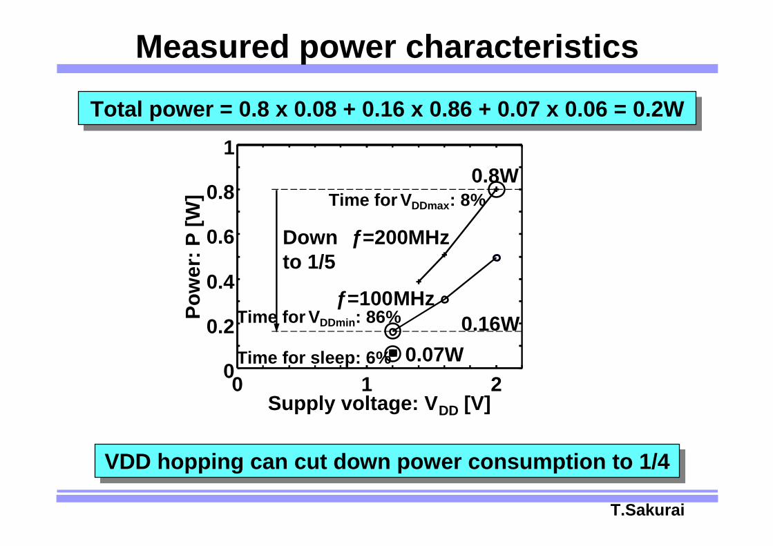
Measured power characteristics
Total power = 0.8 x 0.08 + 0.16 x 0.86 + 0.07 x 0.06 = 0.2WTotal power = 0.8 x 0.08 + 0.16 x 0.86 + 0.07 x 0.06 = 0.2W
VDD hopping can cut down power consumption to 1/4VDD hopping can cut down power consumption to 1/4
0.8W
0
0.2
0.4
0.6
0.8
1
Supply voltage: VDD [V]
Pow
er: P
[W]
0 1 2
ƒ=100MHz
ƒ=200MHz
0.16W
Downto 1/5
Time for sleep: 6% 0.07W
Time for VDDmin: 86%
Time for VDDmax: 8%
T.SakuraiT.Sakurai
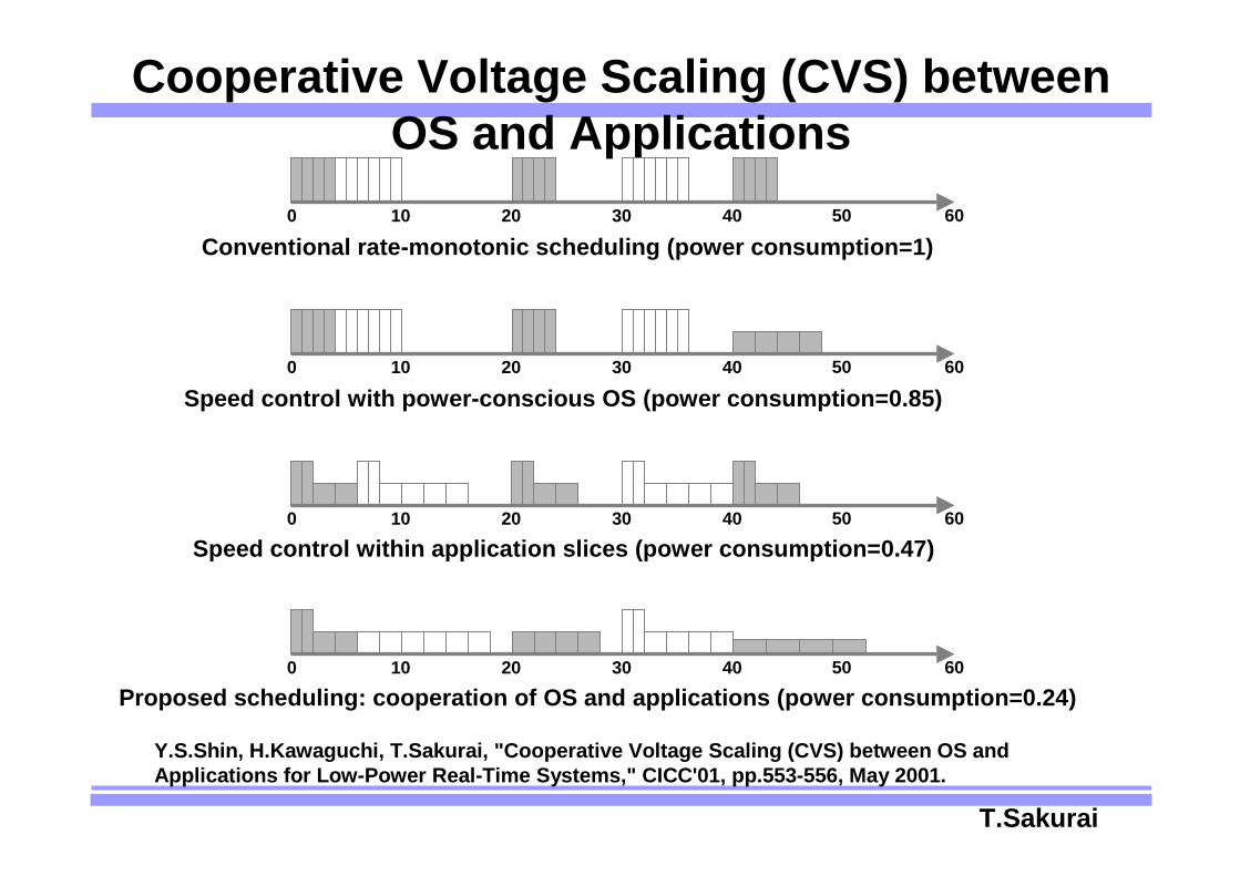
Cooperative Voltage Scaling (CVS) between OS and Applications
0 10 3020 40 50 60
Proposed scheduling: cooperation of OS and applications (power consumption=0.24)
0 10 3020 40 50 60
Speed control within application slices (power consumption=0.47)
0 10 3020 40 50 60
Conventional rate-monotonic scheduling (power consumption=1)
0 10 3020 40 50 60
Speed control with power-conscious OS (power consumption=0.85)
Y.S.Shin, H.Kawaguchi, T.Sakurai, "Cooperative Voltage Scaling (CVS) between OS and Applications for Low-Power Real-Time Systems," CICC'01, pp.553-556, May 2001.
T.SakuraiT.Sakurai
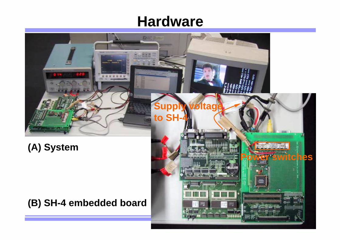
Power switches
Supply voltage to SH-4
(B) SH-4 embedded board
(A) System
Hardware
T.SakuraiT.Sakurai
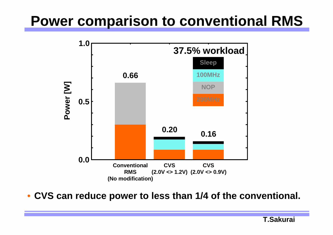
Power comparison to conventional RMS
ConventionalRMS
(No modification)
CVS(2.0V <> 1.2V)
CVS(2.0V <> 0.9V)
0.0
0.5
1.0
Pow
er [W
]Sleep
100MHz
NOP
200MHz
0.66
0.20 0.16
• CVS can reduce power to less than 1/4 of the conventional.
37.5% workload
T.SakuraiT.Sakurai
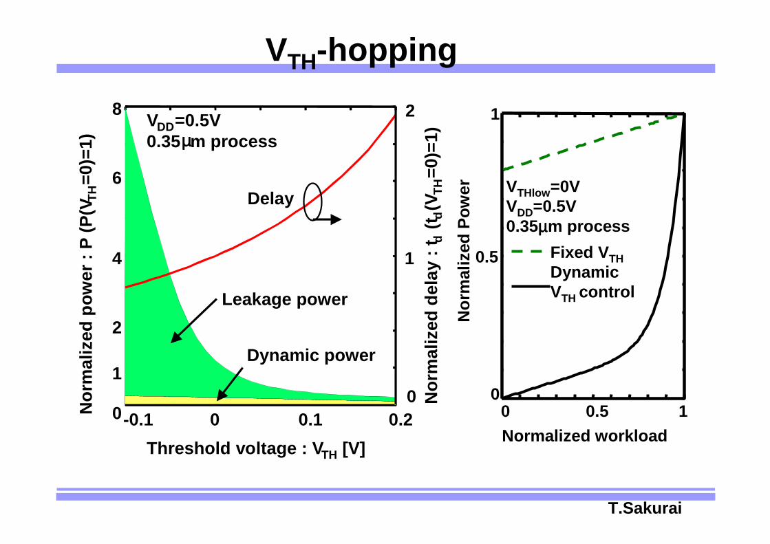
VTH-hopping
-0.1 0 0.1 0.20
1
2
4
6
8
1
0
2
Dynamic power
Delay
Leakage power
Nor
mal
ized
del
ay :
t d(t d
(VTH
=0)=
1)
Nor
mal
ized
pow
er :
P (P
(VTH
=0)=
1)
Threshold voltage : VTH [V]
VDD=0.5V0.35µµµµm process
Fixed VTHDynamic VTH control
Normalized workloadN
orm
aliz
ed P
ower
0 0.5 10
0.5
1
VTHlow=0VVDD=0.5V0.35µµµµm process
T.SakuraiT.Sakurai
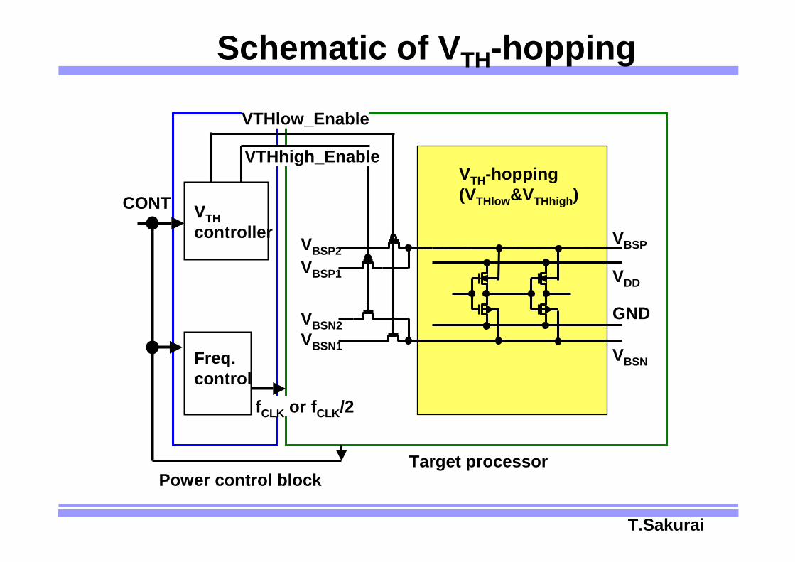
Schematic of VTH-hopping
VTHcontroller
Freq. control
CONT
fCLK or fCLK/2
VBSP2
Target processor
VTH-hopping(VTHlow&VTHhigh)
Power control block
VBSP1
VBSN2VBSN1
VTHlow_Enable
VTHhigh_Enable
VDD
GND
VBSN
VBSP
T.SakuraiT.Sakurai
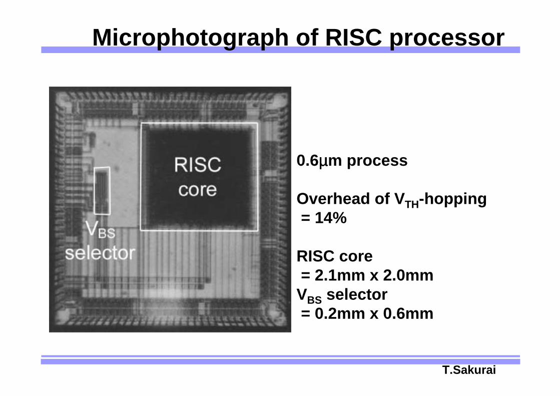
Microphotograph of RISC processor
0.6µµµµm process
Overhead of VTH-hopping= 14%
RISC core = 2.1mm x 2.0mm
VBS selector = 0.2mm x 0.6mm
T.SakuraiT.Sakurai
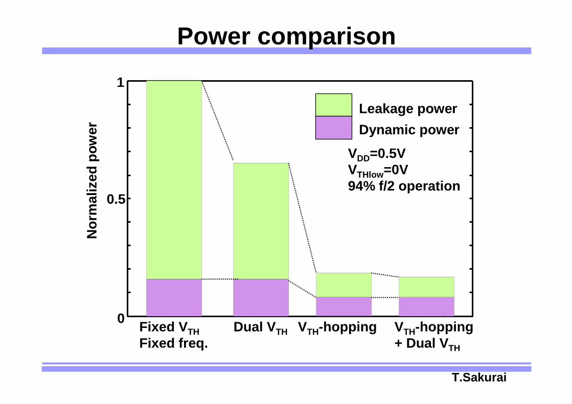
Power comparison
Fixed VTHFixed freq.
Dual VTH0
0.5
1
Leakage powerDynamic power
VDD=0.5VVTHlow=0V94% f/2 operation
Nor
mal
ized
pow
er
VTH-hopping VTH-hopping+ Dual VTH
T.SakuraiT.Sakurai
OutlineLow-power LSI - Through cooperation among levels -
Software
Circuit
Technology
Assembly
LSI
• Introduction
• Technology - Circuit cooperation : Boosted Gate MOS (BGMOS)
• Software - LSI cooperation : VDD / VTH-hopping
• LSI – Assembly cooperation:Superconnect technology
• Summary
T.SakuraiT.Sakurai
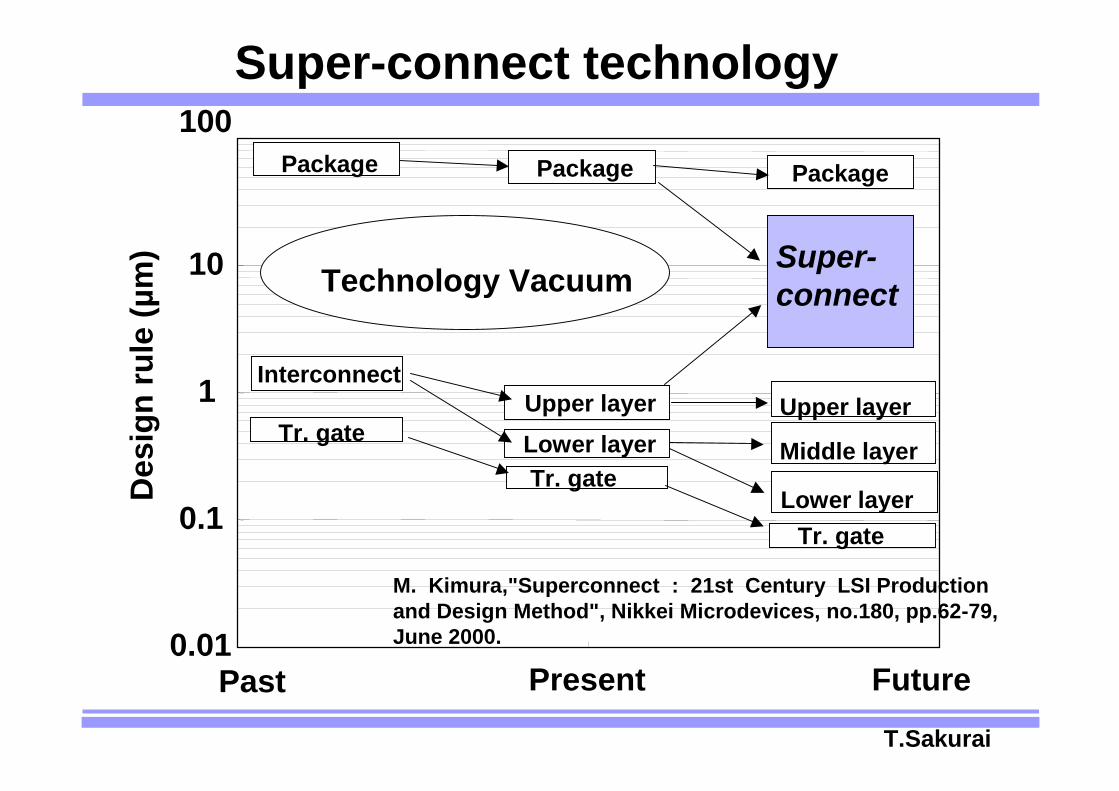
Super-connect technologyD
esig
n ru
le (µ
m)
0.01
0.1
1
10
100
Past Present Future
Tr. gate
Tr. gate
Tr. gate
InterconnectUpper layerLower layer
Upper layer
Middle layer
Lower layer
Super-connect
PackagePackagePackage
Technology Vacuum
M. Kimura,"Superconnect : 21st Century LSI Production and Design Method", Nikkei Microdevices, no.180, pp.62-79, June 2000.
T.SakuraiT.Sakurai
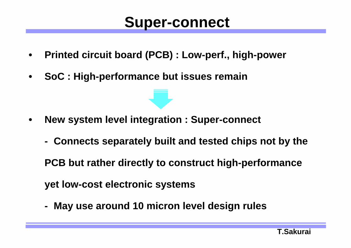
Super-connect
• Printed circuit board (PCB) : Low-perf., high-power
• SoC : High-performance but issues remain
• New system level integration : Super-connect
- Connects separately built and tested chips not by the
PCB but rather directly to construct high-performance
yet low-cost electronic systems
- May use around 10 micron level design rules
T.SakuraiT.Sakurai
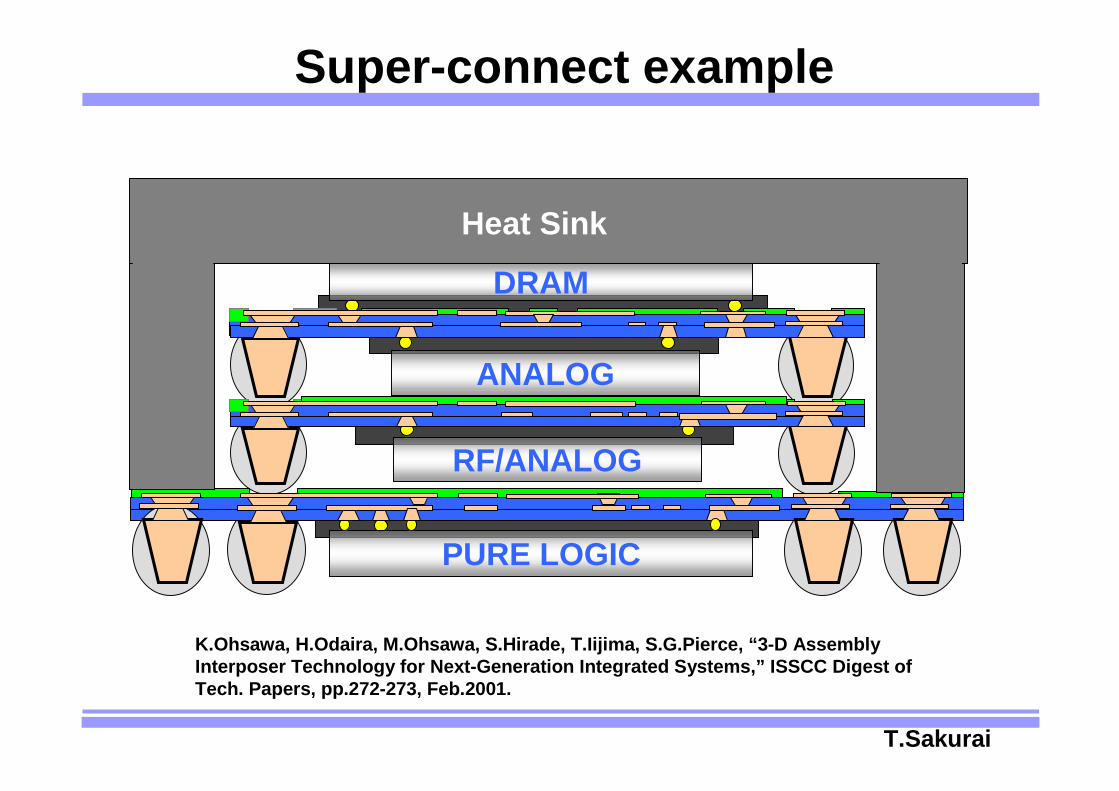
Super-connect example
PURE LOGIC
Heat Sink
ANALOG
RF/ANALOG
DRAM
K.Ohsawa, H.Odaira, M.Ohsawa, S.Hirade, T.Iijima, S.G.Pierce, “3-D Assembly Interposer Technology for Next-Generation Integrated Systems,” ISSCC Digest of Tech. Papers, pp.272-273, Feb.2001.
T.SakuraiT.Sakurai
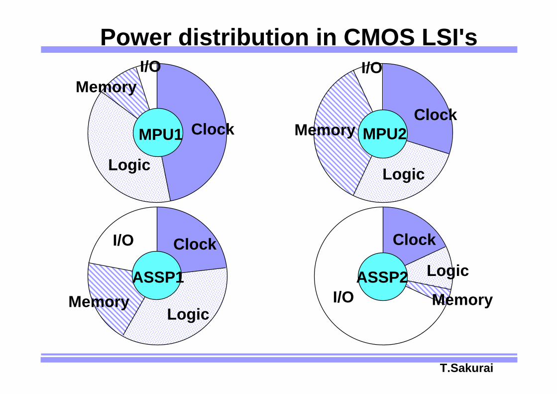
Power distribution in CMOS LSI's
Clock
ASSP1
LogicMemory
I/O
ASSP2
Clock
Logic
MemoryI/O
MPU1 Clock
Logic
MemoryI/O
MPU2Clock
Logic
Memory
I/O
T.SakuraiT.Sakurai
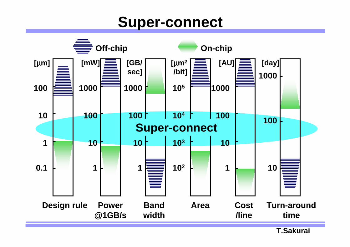
Bandwidth
0.1
1
10
100
Design rule Power@1GB/s
Area
102
103
104
105
[µµµµm] [mW] [GB/sec]
[µµµµm2
/bit]
Super-connect
Off-chip On-chip
1
10
100
1000
Cost/line
[AU]
10
1000[day]
100
Turn-aroundtime
1
10
100
1000
1
10
100
1000
Super-connect
T.SakuraiT.Sakurai
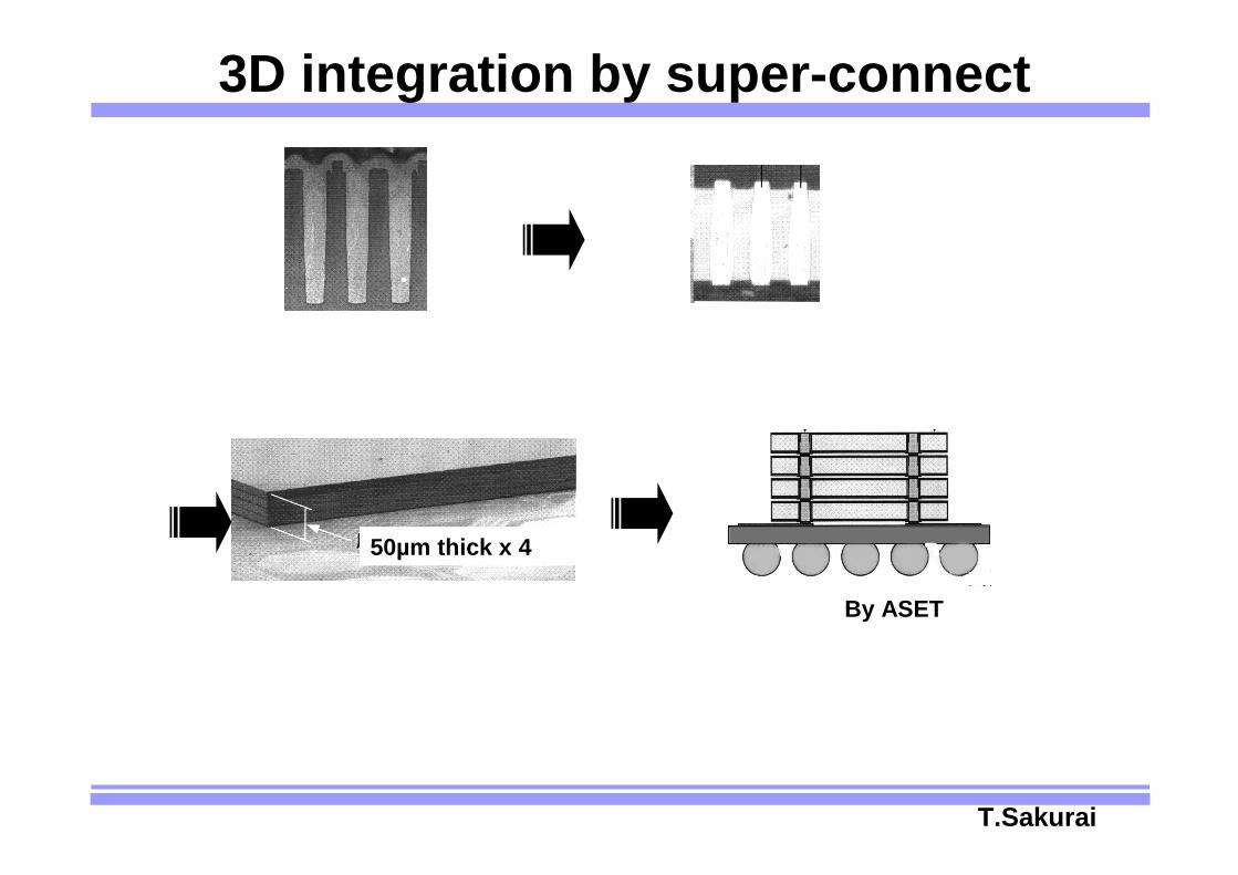
3D integration by super-connect
50µm thick x 4
By ASET
T.SakuraiT.Sakurai
Summary• Power consumption of LSI’s tend to increase due
to the scaling law and due to the leakage increase (sub-threshold, gate tunneling, and junction leakage).
• New trend for low-power LSI’s is to pursue cooperative approaches among levels: BGMOS to cut-off standby leakage, VDD / VTH hopping to reduce operating power, and super-connect to reduce I/O power.
• One of the biggest barriers to the scaling is the leakage power increase and solutions are yet to be discovered.