Embed Size (px)
Citation preview
647International Journal of Scientific Engineering and Technology (ISSN : 2277-1581)
Volume No.3 Issue No.5, pp : 647-650 1 May 2014
IJSET@2014 Page 647
Low Power High Performance Doubletail Comparator
Umamaheswari.V.S.1, Rajaramya.V.G
2
1 PG Scholar,
2Assistant Professor
[email protected],[email protected]
Abstract—Toobtain the low power, delay reduction and high
performance. In this paper, an analysis on the delay of both
conventional dynamic comparator and conventional double
tail dynamic comparator which are called clocked
regenerative comparator will be presented. Designers can
obtain an intuition about the main contributors to the
comparator delay and fully explore the trade off in dynamic
comparator design. Based on, a new dynamic comparator is
proposed, where the circuit of a conventional double tail
comparator is modified for low power and fast operation even
in small supply voltages. Pre –layout simulation results in a
0.18-µm CMOS technology confirm the analysis results. It is
shown that in the proposed dynamic comparator both the
power consumption and delay time are significantly reduced.
Both delay and power consumption can be reduced by adding
few transistors to the proposed comparator. The supply
voltage of 0.8 V, while consuming 9µW in modified
comparator and 12µW in proposed comparator respectively.
Hardware was implemented in FPGA Kit using VHDL
coding.
Keywords—Double tail comparator, low power, fast
operation, Pre-layout simulation, and FPGA. I. Introduction
Comparator is one of the fundamental building blocks in most
analog – to –digital converter. Designing high-speed
comparators is more challenging when the supply voltage is
smaller. In other words to achieve high speed, larger transistors
are required to compensate the reduction of supply voltage,
which also means that more die area and power is needed.
Developing a new circuit structures which avoid stacking too
many transistors between the supply rails is preferable for low
voltage operation, especially if they do not increase the circuit
complexity. Additional circuitry is added to the conventional
dynamic comparator to enhance the comparator speed in low
voltage operation.0.18µm CMOS technology used in tanner
software for simulation.C18 process ensuring very low defect
densities and high yields.0.18µm CMOS technology offers RF
integration, analog mixed signal, digital design flows and high
density system on chip capability. The proposed comparator of
works down to a supply voltage of 0.8V with a maximum clock
frequency consumes 12 µW .Despite the effectiveness of this
approach , the effect of component mismatch in the additional
circuitry on the performance of the comparator should be
considered. The structure of double tail comparator is based on
designing a separate input and cross coupled stage. Based on
the double tail structure proposed a new dynamic comparator is
presented which does not require stacking of too many
transistors.By adding a few minimum size transistors to the
proposed comparator. Latch delay time and mismatch also
reduced. This modification also results in considerable power
saving compared to conventional dynamic comparator and
double tail comparator. In many applications comparator speed,
power dissipation and number of transistors are more
important. If comparator speed is priority, the regenerative
stage could be designed to start its operation from midway
between power supply and ground. There is a wide range of
applications for double tail comparator, they are applied in
different fields such as operational amplifier, predefined
amplifier and analog to digital comparator.it also finds
application in sense amplifier. The main advantage of the
double tail based latched comparators are their fast speed, low
power consumption and adjustable threshold voltage.
II.Material and Methodology EXISTING SYSTEM
A clocked comparator is a circuit element that makes decision
as to whether the input signal is high or low at every clock
cycle. Clocked regenerative comparators make fast decision
due to strong positive feedback in the regenerative latch. Here
analyse the delay of single tail comparator, double tail
comparator and proposed comparator.
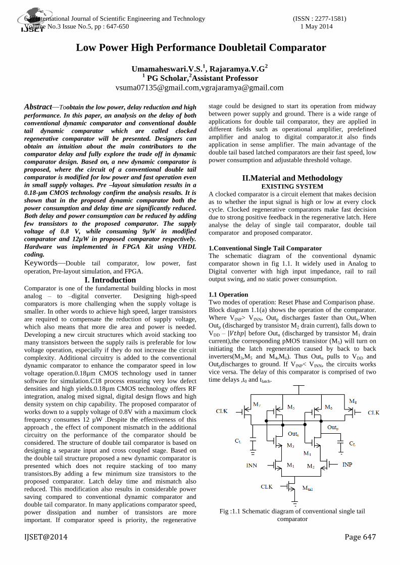
1.Conventional Single Tail Comparator
The schematic diagram of the conventional dynamic
comparator shown in fig 1.1. It widely used in Analog to
Digital converter with high input impedance, rail to rail
output swing, and no static power consumption.
1.1 Operation
Two modes of operation: Reset Phase and Comparison phase.
Block diagram 1.1(a) shows the operation of the comparator.
Where VINP> VINN, Outp discharges faster than Outn.When
Outp (discharged by transistor M2 drain current), falls down to
VDD – 𝑉𝑡ℎ𝑝 before Outn (discharged by transistor M1 drain
current),the corresponding pMOS transistor (M5) will turn on
initiating the latch regeneration caused by back to back
inverters(M3,M5 and M4,M6). Thus Outn pulls to VDD and
Outpdischarges to ground. If VINP< VINN, the circuits works
vice versa. The delay of this comparator is comprised of two
time delays ,t0 and tlatch.
Fig :1.1 Schematic diagram of conventional single tail
comparator
648International Journal of Scientific Engineering and Technology (ISSN : 2277-1581)
Volume No.3 Issue No.5, pp : 647-650 1 May 2014
IJSET@2014 Page 648
Block Diagram: 1.1.1
The delay t0 represents the capacitive discharge of the load
capacitance CL until the first p channel transistor (M5/M6) turn
On. The second term,tlatch , is the latching delay of two cross
coupledinverters. Voltage swing ∆Vout = VDD/2 has to be
obtained from an initial output voltage difference ∆V0 at the
falling output.
tdelay = t0+tlatch
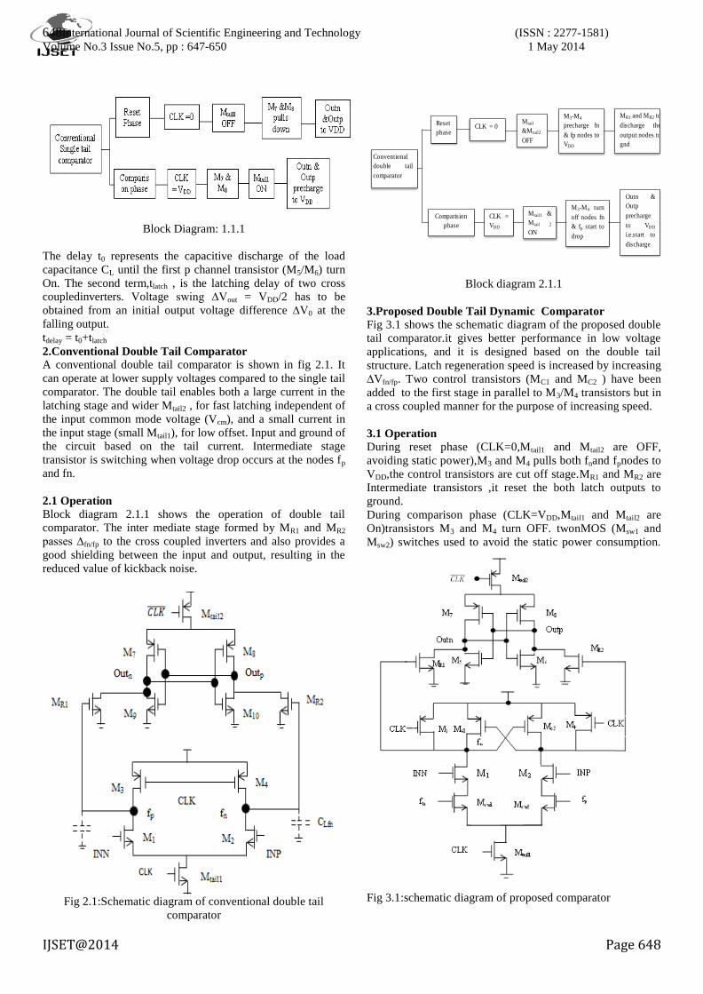
2.Conventional Double Tail Comparator
A conventional double tail comparator is shown in fig 2.1. It
can operate at lower supply voltages compared to the single tail
comparator. The double tail enables both a large current in the
latching stage and wider Mtail2 , for fast latching independent of
the input common mode voltage (Vcm), and a small current in
the input stage (small Mtail1), for low offset. Input and ground of
the circuit based on the tail current. Intermediate stage
transistor is switching when voltage drop occurs at the nodes fp
and fn.
2.1 Operation
Block diagram 2.1.1 shows the operation of double tail
comparator. The inter mediate stage formed by MR1 and MR2
passes ∆fn/fp to the cross coupled inverters and also provides a
good shielding between the input and output, resulting in the
reduced value of kickback noise.
Fig 2.1:Schematic diagram of conventional double tail
comparator
Block diagram 2.1.1
3.Proposed Double Tail Dynamic Comparator
Fig 3.1 shows the schematic diagram of the proposed double
tail comparator.it gives better performance in low voltage
applications, and it is designed based on the double tail
structure. Latch regeneration speed is increased by increasing
∆Vfn/fp. Two control transistors (MC1 and MC2 ) have been
added to the first stage in parallel to M3/M4 transistors but in
a cross coupled manner for the purpose of increasing speed.
3.1 Operation
During reset phase (CLK=0,Mtail1 and Mtail2 are OFF,
avoiding static power),M3 and M4 pulls both fnand fpnodes to
VDD,the control transistors are cut off stage.MR1 and MR2 are
Intermediate transistors ,it reset the both latch outputs to
ground.
During comparison phase (CLK=VDD,Mtail1 and Mtail2 are
On)transistors M3 and M4 turn OFF. twonMOS (Msw1 and
Msw2) switches used to avoid the static power consumption.
Fig 3.1:schematic diagram of proposed comparator
Conventional
double tail
comparator
Reset
phase
Comparision
phase
CLK = 0
CLK =
VDD
Mtail
&Mtail2
OFF
M3-M4
precharge fn
& fp nodes to
VDD
MR1 and MR2 to
discharge the
output nodes to
gnd
Mtail1 &
Mtail 2
ON
M3-M4 turn
off nodes fn
& fp start to
drop
Outn &
Outp
precharge
to VDD
i.e.start to
discharge
649International Journal of Scientific Engineering and Technology (ISSN : 2277-1581)
Volume No.3 Issue No.5, pp : 647-650 1 May 2014
IJSET@2014 Page 649
Proposed comparator enhances the speed of the double tail
comparator by affecting two factors such as increases the
initial output voltage difference at the beginning of
regeneration (t=t0); and it enhances the effective trans
conductance.
MODIFICATION
Fig 4 shows the schematic diagram of modified comparator .it
is designed based on the proposed comparator.compared with
proposed it provides, better performance of double tail
comparator in low voltage applications. Drawback of
proposed comparator is ,the nodes fn and fp starts to drop with
different rates according to the input voltages. The continues
falling of fn, the corresponding transistor MC1 starts to turn on
and fp node backs to VDD. Node fn to be discharged
completely(MC2 off).When one of the control transistors (MC1)
turns ON,a current from VDD is drawn to the ground via input
and tail transistor. Resulting a static power consumption. For
this purpose two switching transistors (Msw3 and Msw4) have
been added to Msw1 and Msw2 in series manner. Modified
comparator reduced the delay and power.
4.1.Operation
Operation of modification in both reset and comparison phase
is similar as proposed comparator .At the beginning of the
decision making phase, both fn and fp nodes have been
precharged to VDD.in the reset phase switches are closed , fn
and fp starts to drop with different discharging rates. As soon
as comparator detects that one of the fn/fp nodes is discharging
faster, control transistors will act in a way to increase their
voltage difference. Iffp is pulling up to VDD and fn should be
discharged completely , hence switching in the charging path
of fp will be opened but the other switch connected to fn will be
closedto allow the complete discharge of fn node. The
operation of the control transistors with the switches emulates
the operation of the latch.
Fig 4 :Schematic diagram of Modified Comparator
4.2. Design Considerations
The size of transistors can be determined by the time it takes
that one of the control transistors turns on must be smaller than
t0(regeneration time).It can be achieved by designing first
and second stage of tail currents. Low threshold pMOS
devices can be used as control transistors leading to faster
turn on in the fabrication technology.another consideration is
effect of mismatch between the controlling transistorsof the
comparator. Mismatch is a spatial noise spread. In this
modification mismatch effect is reduced. The large voltage
variations in the internal nodes are coupled to the input
disturbing the input voltage called ―kick back noise‖. Most
efficient comparators generate this type of noise. The
minimum kickback noise in the double tail comparator.
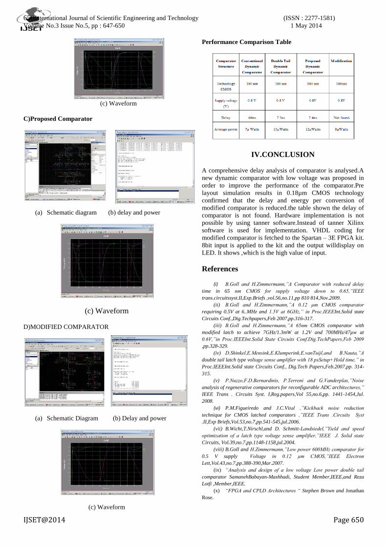
III.Results and Table Tanner Software (Pre layout simulation)is used for
simulation. In order to compare the modified comparator with
the Single tail ,double tail and proposed comparators. All
circuits have been simulated in a 0.18µm CMOS technology
with VDD = 0.8V.The delay of modified comparator is
significantly reduced in low voltage supplies. By decreasing
the supply voltage, structures are start to behave differently.
The double tail comparator can operate faster and can be used
in low supply voltages, while consuming nearly the same
power as the conventional (single tail) comparator. The case
is even better for the modified comparator when compared to
the conventional dynamic comparator. Finally table 1
compares the performance of modified comparator with the
conventional, double tail and proposed comparator.
A) Conventional (Single Tail)Comparator
a) Schematic diagramb)Delay and power
(c) Waveform
B)Double Tail Comparator
(a) Schematic diagram (b) Delay and Power
650International Journal of Scientific Engineering and Technology (ISSN : 2277-1581)
Volume No.3 Issue No.5, pp : 647-650 1 May 2014
IJSET@2014 Page 650
(c) Waveform
C)Proposed Comparator
(a) Schematic diagram (b) delay and power
(c) Waveform
D)MODIFIED COMPARATOR
(a) Schematic Diagram (b) Delay and power
(c) Waveform
Performance Comparison Table
IV.CONCLUSION
A comprehensive delay analysis of comparator is analysed.A
new dynamic comparator with low voltage was proposed in
order to improve the performance of the comparator.Pre
layout simulation results in 0.18µm CMOS technology
confirmed that the delay and energy per conversion of
modified comparator is reduced.the table shown the delay of
comparator is not found. Hardware implementation is not
possible by using tanner software.Instead of tanner Xilinx
software is used for implementation. VHDL coding for
modified comparator is fetched to the Spartan – 3E FPGA kit.
8bit input is applied to the kit and the output willdisplay on
LED. It shows ,which is the high value of input.
References
(i) B.Goll and H.Zimmermann,”A Comparator with reduced delay
time in 65 nm CMOS for supply voltage down to 0.65,”IEEE
trans.circuitssyst.II,Exp.Briefs ,vol.56,no.11,pp 810 814,Nov.2009.
(ii) B.Goll and H.Zimmermann,”A 0.12 µm CMOS comparator
requiring 0.5V at 6..MHz and 1.5V at 6GHz,” in Proc.IEEEInt.Solid state
Circuits Conf.,Dig.Techpapers,Feb 2007,pp.316-317.
(iii) B.Goll and H.Zimmermann,”A 65nm CMOS comparator with
modified latch to achieve 7GHz/1.3mW at 1.2V and 700MHz/47µw at
0.6V,”in Proc.IEEEInt.Solid State Circuits Conf.Dig.TechPapers,Feb 2009
,pp.328-329.
(iv) D.Shinkel,E.Mensink,E.Klumperink,E.vanTuijl,and B.Nauta,”A
double tail latch type voltage sense amplifier with 18 psSetup+Hold time,” in
Proc.IEEEInt.Solid state Circuits Conf., Dig.Tech Papers,Feb.2007,pp. 314-
315.
(v) P.Nuzzo,F.D.Bernardinis, P.Terreni and G.Vanderplas,”Noise
analysis of regenerative comparators for reconfigurable ADC architectures,”
IEEE Trans . Circuits Syst. I,Reg.papers,Vol 55,no.6,pp. 1441-1454,Jul.
2008.
(vi) P.M.Figueiredo and J.C.Vital ,”Kickback noise reduction
technique for CMOS latched comparators ,”IEEE Trans .Circuits Syst
.II,Exp Briefs,Vol.53,no.7,pp.541-545,jul.2006.
(vii) B.Wicht,T.Nirschl,and D. Schmitt-Landsiedel,”Yield and speed
optimization of a latch type voltage sense amplifier,”IEEE J. Solid state
Circuits, Vol.39,no.7,pp.1148-1158,jul.2004.
(viii) B.Goll and H.Zimmermann,”Low power 600MHz comparator for
0.5 V supply Voltage in 0.12 µm CMOS,”IEEE Electron
Lett,Vol.43,no.7,pp.388-390,Mar.2007.
(ix) “Analysis and design of a low voltage Low power double tail
comparator SamanehBabayan-Mashhadi, Student Member,IEEE,and Reza
Lotfi ,Member,IEEE.
(x) “FPGA and CPLD Architectures “ Stephen Brown and Jonathan
Rose.


![A Fast Dynamic 64-bit Comparator with Small …downloads.hindawi.com/journals/vlsi/2002/535394.pdf · A Fast Dynamic 64-bit Comparator with Small Transistor ... phase logic [6] and](https://img.pdfslide.us/doc/110x75/5b7b4e627f8b9adb4c8c5a76/a-fast-dynamic-64-bit-comparator-with-small-a-fast-dynamic-64-bit-comparator.jpg)