Embed Size (px)
Citation preview

200 IEEE TRANSACTIONS ON CIRCUITS AND SYSTEMS—II: EXPRESS BRIEFS, VOL. 58, NO. 4, APRIL 2011
Low-Power Divider Retiming in a3–4 GHz Fractional-N PLL
Davide Tasca, Marco Zanuso, Member, IEEE, Salvatore Levantino, Member, IEEE,Carlo Samori, Senior Member, IEEE, and Andrea L. Lacaita, Fellow, IEEE
Abstract—The resynchronization of a frequency divider outputis routinely used in the design of low-noise phase-locked loops(PLLs) in order to remove additional phase noise and avoidmodulus-dependent nonlinearity. However, metastability issuescause PLLs to fail to lock or to degrade jitter at certain synthe-sized frequencies. This brief proposes a novel automatic retimingcircuit, which mitigates metastability issues and avoids inducednoise degradation, without adding a relevant increase in powerconsumption. A 3–4-GHz PLL implementing this technique hasbeen fabricated in 65-nm CMOS technology. Measured root meansquare jitter below 500 fsec over the whole tuning range andadded current consumption of 51 μA from a voltage supply of1.2 V prove the effectiveness of the proposed solution.
Index Terms—Frequency synthesizer, metastability, phase-locked loop (PLL), synchronization.
I. INTRODUCTION
IN FREQUENCY synthesizers, based on phase-locked loops(PLLs), a programmable frequency divider is needed to
obtain the desired frequency multiplication. Power consump-tion limitations lead typically to adopt asynchronous countersinstead of synchronous ones in the design of the frequencydivider. As a result, a certain delay τ between the input andoutput rising edges of the divider exists, which depends onprocess–voltage–temperature (PVT) conditions and moduluscontrol. The adoption of asynchronous dividers gives rise to twomain disadvantages: jitter accumulation along divider stages,which increases PLL phase noise [1], and a modulus-dependentdivider delay (MDDD), which gives rise to spurs and additionalphase noise [2].
Synchronizing the divider output to the voltage-controlled-oscillator (VCO) signal solves those issues. The jitter accu-mulated along the divider chain is canceled out, and the onlyadded jitter comes from the resynchronizing flip-flop [3]. TheMDDD effect is greatly mitigated since the dependence ofthe divider delay on modulus control is masked by the resyn-chronization. However, synchronization suffers from potentialmetastability. Methods proposed in [2] and [4] derive a retimed
Manuscript received November 11, 2010; revised January 19, 2011; acceptedJanuary 30, 2011. Date of current version April 20, 2011. This work wasrecommended by Associate Editor P.-I. Mak.
D. Tasca, S. Levantino, C. Samori, and A. L. Lacaita are with the Departmentof Electronics and Information, Politecnico di Milano, 20133 Milano, Italy(e-mail: [email protected]).
M. Zanuso was with the Politecnico di Milano, 20133 Milano, Italy. He isnow with the Department of Electrical Engineering, University of California,Los Angeles, CA 90095 USA (e-mail: [email protected]).
Color versions of one or more of the figures in this letter are available onlineat http://ieeexplore.ieee.org.
Digital Object Identifier 10.1109/TCSII.2011.2124510
Fig. 1. PLL block schematic with the synchronization of a divider output.
divider output by combining properly the internal signals ofan asynchronous divider chain. Other methods are based ondetecting a metastable state and retiming the divider output bychoosing between synchronizing with either the VCO outputor the inverse of the VCO output [5]. All those approacheshave the disadvantage of requiring additional flip-flops, whichneed to operate continuously at high frequency. Thus, theyadd a nonnegligible power consumption penalty. This briefpresents an automatic retiming circuit based on a digital controlloop, which regulates the delay of the frequency divider. Theproposed method [6] avoids both metastability issues and al-lows powering down all ancillary circuits after calibration, thusadding a negligible power consumption increase.
This brief is organized as follows. Section II introduces theissues associated with unregulated retiming. Section III de-scribes the concept and the operation of the proposed retimingregulation. Section IV shows the circuit design, and Section Vshows the simulation results. The experimental results arepresented in Section VI, and finally, Section VII draws theconclusions.
II. ISSUES IN DIVIDER RETIMING
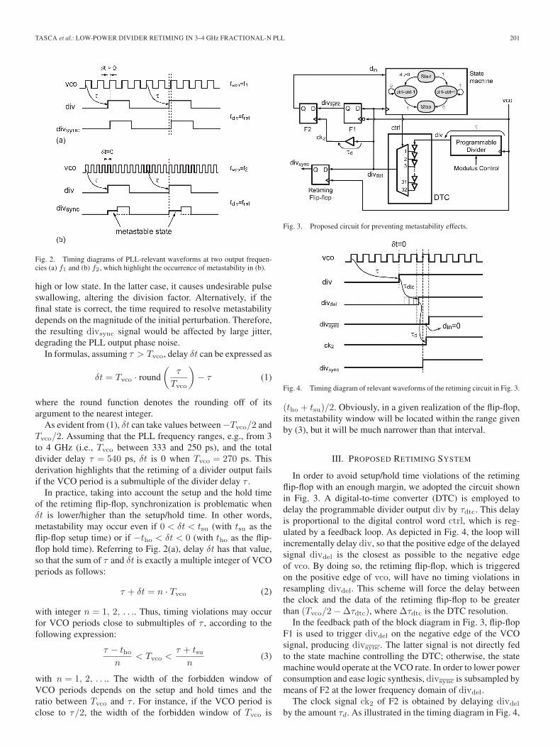
We can refer to the scheme shown in Fig. 1, where the outputof the divider is sampled using a vco signal as a clock. Letus define as δt the delay occurring between the nearest risingedge of the VCO signal and the rising edge of div. If the delayτ introduced by the programmable divider is greater than oneVCO period Tvco, δt depends on VCO frequency. As illustratedin Fig. 2(a), a nonzero δt value exists for fvco = f1, and anenough margin exists to sample the div signal. The δt delay isinstead 0 for fvco = f2 [see Fig. 2(b)], and the D flip-flop usedfor the divider output resampling will enter its metastable state(assuming, for the sake of simplicity, the setup and hold timesof the flip-flop to be zero). The flip-flop can evolve either to its
1549-7747/$26.00 © 2011 IEEE
TASCA et al.: LOW-POWER DIVIDER RETIMING IN 3–4 GHz FRACTIONAL-N PLL 201
Fig. 2. Timing diagrams of PLL-relevant waveforms at two output frequen-cies (a) f1 and (b) f2, which highlight the occurrence of metastability in (b).
high or low state. In the latter case, it causes undesirable pulseswallowing, altering the division factor. Alternatively, if thefinal state is correct, the time required to resolve metastabilitydepends on the magnitude of the initial perturbation. Therefore,the resulting divsync signal would be affected by large jitter,degrading the PLL output phase noise.
In formulas, assuming τ > Tvco, delay δt can be expressed as
δt = Tvco · round
(τ
Tvco
)− τ (1)
where the round function denotes the rounding off of itsargument to the nearest integer.
As evident from (1), δt can take values between −Tvco/2 andTvco/2. Assuming that the PLL frequency ranges, e.g., from 3to 4 GHz (i.e., Tvco between 333 and 250 ps), and the totaldivider delay τ = 540 ps, δt is 0 when Tvco = 270 ps. Thisderivation highlights that the retiming of a divider output failsif the VCO period is a submultiple of the divider delay τ .
In practice, taking into account the setup and the hold timeof the retiming flip-flop, synchronization is problematic whenδt is lower/higher than the setup/hold time. In other words,metastability may occur even if 0 < δt < tsu (with tsu as theflip-flop setup time) or if −tho < δt < 0 (with tho as the flip-flop hold time). Referring to Fig. 2(a), delay δt has that value,so that the sum of τ and δt is exactly a multiple integer of VCOperiods as follows:
τ + δt = n · Tvco (2)
with integer n = 1, 2, . . .. Thus, timing violations may occurfor VCO periods close to submultiples of τ , according to thefollowing expression:
τ − tho
n< Tvco <
τ + tsun
(3)
with n = 1, 2, . . .. The width of the forbidden window ofVCO periods depends on the setup and hold times and theratio between Tvco and τ . For instance, if the VCO period isclose to τ/2, the width of the forbidden window of Tvco is
Fig. 3. Proposed circuit for preventing metastability effects.
Fig. 4. Timing diagram of relevant waveforms of the retiming circuit in Fig. 3.
(tho + tsu)/2. Obviously, in a given realization of the flip-flop,its metastability window will be located within the range givenby (3), but it will be much narrower than that interval.
III. PROPOSED RETIMING SYSTEM
In order to avoid setup/hold time violations of the retimingflip-flop with an enough margin, we adopted the circuit shownin Fig. 3. A digital-to-time converter (DTC) is employed todelay the programmable divider output div by τdtc. This delayis proportional to the digital control word ctrl, which is reg-ulated by a feedback loop. As depicted in Fig. 4, the loop willincrementally delay div, so that the positive edge of the delayedsignal divdel is the closest as possible to the negative edgeof vco. By doing so, the retiming flip-flop, which is triggeredon the positive edge of vco, will have no timing violations inresampling divdel. This scheme will force the delay betweenthe clock and the data of the retiming flip-flop to be greaterthan (Tvco/2 − Δτdtc), where Δτdtc is the DTC resolution.
In the feedback path of the block diagram in Fig. 3, flip-flopF1 is used to trigger divdel on the negative edge of the VCOsignal, producing divsync. The latter signal is not directly fedto the state machine controlling the DTC; otherwise, the statemachine would operate at the VCO rate. In order to lower powerconsumption and ease logic synthesis, divsync is subsampled bymeans of F2 at the lower frequency domain of divdel.
The clock signal ck2 of F2 is obtained by delaying divdel
by the amount τd. As illustrated in the timing diagram in Fig. 4,

202 IEEE TRANSACTIONS ON CIRCUITS AND SYSTEMS—II: EXPRESS BRIEFS, VOL. 58, NO. 4, APRIL 2011
τd has to satisfy two constraints. On one hand, it has to be lesserthan the VCO period. Otherwise, the rising edge of ck2 wouldoccur after the rising edge of divsync, and the output din of F2would be always logical level 1 for any δt. On the other hand,τd has to be greater than the propagation delay of F1; otherwise,ck2 would always sample logical level 0 for any δt.
The state machine whose flow chart is shown in Fig. 3is employed in place of a plain digital integrator. The lattersolution would produce a periodic control signal ctrl at thesteady state of the feedback loop, which would inevitably giverise to a spur in the output spectrum of the PLL in Fig. 1[7]. Instead, the implemented state machine accumulates theinput error signal din in the ctrl register. This accumulation isperformed until din toggles. When the first toggle of din occurs,the value of ctrl is not changed anymore, and the algorithmends. This solution has two main advantages: It avoids limitcycles, and it allows switching off the ancillary circuits usedfor retiming (namely, F1, F2, the delay block τd, and the statemachine) once calibration ends.
IV. CIRCUIT DESIGN
A fractional-N frequency synthesizer implementing the pro-posed retiming system has been designed in a 65-nm CMOSprocess. The VCO is based on a fully-integrated LC resonatorand its frequency ranges between about 3 and 4 GHz. Sincethe reference frequency is 40 MHz, the programmable dividermodulus must range between N = 75 and N = 100. The pro-grammable divider is implemented as a chain of six dividers-by-2/3, and modulus N given by (64 + 20 · N0 + · · · +25 · N5) can span from 64 to 127 [8]. The use of True SinglePhase Clock (TSPC) logic limits the average supply currentof the programmable divider to 410 μA (at maximum inputfrequency).
The implementation of the proposed retiming system needsa DTC with proper range and resolution over PVT variations.Its full-scale (FS) range needs to be greater than the maximumVCO period, so that at least one of the DTC phases is close tothe falling edge of the vco signal. The DTC delay resolutionΔτdtc needs to be so fine that the minimum delay between theclock and the data of the retiming flip-flop (Tvco/2 − Δτdtc) islarger than the flip-flop setup and hold times.
The DTC is implemented as the combination of a delayline (DL) and a multiplexer (MUX). The DL is a chain of32 buffers, i.e., each one with a delay Δτdtc value of 24 psin the typical process corner. This delay resolution decreases to18 ps in the fast corner (with fast-fast transistors, low temper-ature, and maximum voltage supply) and increases to 35 ps inthe slow corner (with slow-slow transistors, high temperature,and minimum voltage supply). Thus, on one hand, a DTCFS range of 576 ps in the fast corner covers with margin themaximum Tvco value, i.e., 333 ps. On the other hand, the DTCresolution of 35 ps in the slow corner guarantees a minimumdelay between the clock and the data of the retiming flip-flop of(125 − 35) ps = 90 ps, which is larger than the flip-flop setupand hold times.
Each delay element of the DTC consists of two CMOSinverters. The MUX, implemented with CMOS standard cells,
Fig. 5. Relevant waveforms of the retiming circuit in Fig. 3 from the mixed-mode transient simulations.
selects the phase according to the 5-b control word ctrl.Since the DTC is implemented in CMOS and it operates onthe low-frequency div signal, it drains an average current ofonly 51 μA. Mismatches in the delay elements of the DTCand the stages of the MUX cause nonlinearity in the DTCconversion characteristic. Proper design and layout of theDTC allowed to keep the mismatches lower than the DTC res-olution (18 ps in the fast corner), so that the DTC characteristicis monotonic over a 3σ variation of the device parameters.
The three flip-flops in Fig. 3 are implemented in source-coupled logic topology with a master–slave configuration.Compared with single-ended implementations, it has muchhigher immunity to supply noise, which can worsen the phasenoise performance of a PLL. The differential topology allowsto simply swap the differential clock inputs in order to realizethe negative-edge-triggered flip-flop. Since flip-flop clock fre-quency is the VCO frequency, their bias current is as high as188 μA. However, due to the proposed retiming circuit, F1 andF2 are powered down when the calibration ends, limiting powerconsumption only to the retiming flip-flop.
The τd delay block is the cascade of two differential stages:the first one loaded by a poly/n-well capacitor and the secondone restoring the steep slope of the div signal. The stage isdesigned to introduce a delay of 150 ps that guarantees correctresampling of divsync. Its bias current is about 132 μA, but it ispowered down at the end of calibration.
V. CIRCUIT SIMULATIONS
Fig. 5 shows the mixed-mode simulations of the retimingsystem in Fig. 3, when the VCO oscillates at a frequency of3.6 GHz and N is set to 90. After the reset signal of the statemachine is released, the integration of ctrl starts. When din
toggles, the algorithm stops. Even if din toggles again, nothingchanges.
Fig. 6 shows the waveforms of the retiming flip-flop frompostlayout circuit simulations. Fig. 6(a) shows what happenswhen the rising edge divdel falls inside the flip-flop metasta-bility window. This situation occurs for a particular choice ofthe VCO frequency. As evident, signal divsync is not correctlyresampled. After calibration [see Fig. 6(b)], the rising edgeof divdel is moved out of the metastability window, and theresampling is correct.
The average current consumption of the divider and theretiming system blocks is summarized in Table I. After cal-ibration, the overhead of the divider current consumption

TASCA et al.: LOW-POWER DIVIDER RETIMING IN 3–4 GHz FRACTIONAL-N PLL 203
Fig. 6. Waveforms of inputs and the output of the retiming flip-flop from thefollowing circuit simulations: (a) before and (b) after calibration.
TABLE IAVERAGE CURRENT CONSUMPTION
Fig. 7. Photograph of the circuit in Fig. 3.
introduced by the proposed retiming system is only representedby the DTC, whose average current is equal to 51 μA (only anincrease of 8% on the total current).
The retiming algorithm needs to be rerun when the PLLdivision factor N is changed. However, the time required forcalibration is given at most by the number of DTC phasestimes the reference clock period, i.e., 32 · Tref = 800 ns, whichdoes not represent a limitation in practical cases. If the PLLsynthesized frequency is instead not varied, there is no needto rerun the algorithm even in the presence of voltage supplyor temperature variations. As confirmed from the circuit sim-ulations, a typical voltage supply fluctuation of ±10% of itsnominal value causes the dynamic range of the DTC to vary byabout ±76 ps. Thus, even in the worst case in which the lastphase of the DTC is selected, the DTC delay variation is lowerthan the minimum Tvco/2 (i.e., 125 ps), and it causes no setupor hold violations.
VI. IMPLEMENTATION AND MEASUREMENTS
The PLL including the described automatic retiming circuithas been fabricated in a 65-nm CMOS process with a voltagesupply of 1.2 V. The retiming circuit, whose microphotographis shown in Fig. 7, occupies an area of 2700 μm2. The test chipallows to enable or disable the described automatic retimingcircuit. Moreover, calibration automatically restarts wheneverthe divider modulus control is changed by the user.
The PLL performance has been first measured when theretiming circuit is disabled. The jitter obtained from the phase
Fig. 8. Measured PLL jitter (integrated from 3 kHz to 30 MHz) versus outputfrequency when the proposed retiming circuit is disabled (hollow circles) andwhen it is enabled (filled circles). At about 3.78 GHz, the PLL loses lock whenretiming is disabled.
Fig. 9. Measured PLL spectrum at 3.78 GHz when the retiming circuit isenabled (after calibration).
spectrum integration from 3 kHz to 30 MHz is plotted as afunction of the output frequency in Fig. 8. The root meansquare (RMS) jitter is lower than 500 fs along almost the wholerange, but it has a sudden increase at about 3.78 GHz, wherethe PLL loses lock (hollow circles). This measurement resultdemonstrates the harmful effect of metastability on PLL noiseperformance.
Once the retiming system is enabled, the DTC delay isadapted properly, and the metastability of the retiming flip-flopis prevented. In this case, the loop locks over the whole rangeeven at 3.78 GHz with 500-fs absolute RMS jitter (see filledcircles in Fig. 8). The spectrum at that frequency, measuredwhen the retiming circuit is enabled, is shown in Fig. 9.
VII. CONCLUSION
Retiming of frequency dividers in PLLs eliminates the di-vider contribution to phase noise and avoids the effects of theMDDD. A novel system has been described that avoids timingviolations in the retiming flip-flop and allows powering downmost of the ancillary circuits. The method is demonstrated ina 65-nm CMOS frequency synthesizer in the 3–4-GHz range,which exhibits integrated RMS jitter lower than 500 fs overthe whole tuning range. The retiming circuit after calibrationincreases the average current consumption by 51 μA.
204 IEEE TRANSACTIONS ON CIRCUITS AND SYSTEMS—II: EXPRESS BRIEFS, VOL. 58, NO. 4, APRIL 2011
REFERENCES
[1] W. Egan, “Modeling phase noise in frequency dividers,” IEEE Trans.Ultrason., Ferroelectr., Freq. Control, vol. 37, no. 4, pp. 307–315, Jul. 1990.
[2] S. Pamarti, L. Jansson, and I. Galton, “A wideband 2.4 GHz ΔΣ fractional-N PLL with 1 Mb/s in-loop modulation,” IEEE J. Solid-State Circuits,vol. 39, no. 1, pp. 49–62, Jan. 2004.
[3] S. Levantino, L. Romanò, S. Pellerano, C. Samori, and A. Lacaita, “Phasenoise in digital frequency dividers,” IEEE J. Solid-State Circuits, vol. 39,no. 5, pp. 775–784, May 2004.
[4] H.-M. Chien, T.-H. Lin, B. Ibrahim, L. Zhang, M. Rofougaran,A. Rofougaran, and W. Kaiser, “A 4 GHz fractional-N synthesizer forIEEE 802.11a,” in VLSI Symp. Tech. Dig., 2004, pp. 46–49.
[5] S. E. Meninger and M. H. Perrott, “A 1-MHz bandwidth 3.6 GHz 0.18 μmCMOS fractional-N synthesizer utilizing a hybrid PFD/DAC structure for
reduced broadband phase noise,” IEEE J. Solid-State Circuits, vol. 41,no. 4, pp. 966–980, Apr. 2006.
[6] D. Tasca, M. Zanuso, S. Levantino, and C. Samori, “An automatic retimingsystem for asynchronous fractional frequency dividers,” in Proc. Conf.Ph.D. Res. Microelectron. Electron., Jul. 2010, pp. 1–4.
[7] M. Zanuso, P. Madoglio, S. Levantino, C. Samori, and A. Lacaita, “Time-to-digital converter for frequency synthesis based on a digital bang-bangDLL,” IEEE Trans. Circuits Syst. I, Reg. Papers, vol. 57, no. 3, pp. 548–555, Mar. 2010.
[8] C. Vaucher, I. Ferencic, M. Locher, S. Sedvallson, U. Voegeli, and Z. Wang,“A family of low-power truly modular programmable dividers in standard0.35-μm CMOS technology,” IEEE J. Solid-State Circuits, vol. 35, no. 7,pp. 1039–1045, Jul. 2000.