Embed Size (px)
Citation preview
© 2005 Microchip Technology Inc. DS51556A
Low Pin Count Demo BoardUser’s Guide
Note the following details of the code protection feature on Microchip devices:
• Microchip products meet the specification contained in their particular Microchip Data Sheet.
• Microchip believes that its family of products is one of the most secure families of its kind on the market today, when used in the intended manner and under normal conditions.
• There are dishonest and possibly illegal methods used to breach the code protection feature. All of these methods, to our knowledge, require using the Microchip products in a manner outside the operating specifications contained in Microchip’s Data Sheets. Most likely, the person doing so is engaged in theft of intellectual property.
• Microchip is willing to work with the customer who is concerned about the integrity of their code.
• Neither Microchip nor any other semiconductor manufacturer can guarantee the security of their code. Code protection does not mean that we are guaranteeing the product as “unbreakable.”
Code protection is constantly evolving. We at Microchip are committed to continuously improving the code protection features of ourproducts. Attempts to break Microchip’s code protection feature may be a violation of the Digital Millennium Copyright Act. If such actsallow unauthorized access to your software or other copyrighted work, you may have a right to sue for relief under that Act.
Information contained in this publication regarding deviceapplications and the like is provided only for your convenienceand may be superseded by updates. It is your responsibility toensure that your application meets with your specifications.MICROCHIP MAKES NO REPRESENTATIONS OR WAR-RANTIES OF ANY KIND WHETHER EXPRESS OR IMPLIED,WRITTEN OR ORAL, STATUTORY OR OTHERWISE,RELATED TO THE INFORMATION, INCLUDING BUT NOTLIMITED TO ITS CONDITION, QUALITY, PERFORMANCE,MERCHANTABILITY OR FITNESS FOR PURPOSE.Microchip disclaims all liability arising from this information andits use. Use of Microchip’s products as critical components inlife support systems is not authorized except with expresswritten approval by Microchip. No licenses are conveyed,implicitly or otherwise, under any Microchip intellectual propertyrights.
DS51556A-page ii
Trademarks
The Microchip name and logo, the Microchip logo, Accuron, dsPIC, KEELOQ, microID, MPLAB, PIC, PICmicro, PICSTART, PRO MATE, PowerSmart, rfPIC, and SmartShunt are registered trademarks of Microchip Technology Incorporated in the U.S.A. and other countries.
AmpLab, FilterLab, Migratable Memory, MXDEV, MXLAB, PICMASTER, SEEVAL, SmartSensor and The Embedded Control Solutions Company are registered trademarks of Microchip Technology Incorporated in the U.S.A.
Analog-for-the-Digital Age, Application Maestro, dsPICDEM, dsPICDEM.net, dsPICworks, ECAN, ECONOMONITOR, FanSense, FlexROM, fuzzyLAB, In-Circuit Serial Programming, ICSP, ICEPIC, Linear Active Thermistor, MPASM, MPLIB, MPLINK, MPSIM, PICkit, PICDEM, PICDEM.net, PICLAB, PICtail, PowerCal, PowerInfo, PowerMate, PowerTool, rfLAB, rfPICDEM, Select Mode, Smart Serial, SmartTel, Total Endurance and WiperLock are trademarks of Microchip Technology Incorporated in the U.S.A. and other countries.
SQTP is a service mark of Microchip Technology Incorporated in the U.S.A.
All other trademarks mentioned herein are property of their respective companies.
© 2005, Microchip Technology Incorporated, Printed in the U.S.A., All Rights Reserved.
Printed on recycled paper.
© 2005 Microchip Technology Inc.
Microchip received ISO/TS-16949:2002 quality system certification for its worldwide headquarters, design and wafer fabrication facilities in Chandler and Tempe, Arizona and Mountain View, California in October 2003. The Company’s quality system processes and procedures are for its PICmicro® 8-bit MCUs, KEELOQ® code hopping devices, Serial EEPROMs, microperipherals, nonvolatile memory and analog products. In addition, Microchip’s quality system for the design and manufacture of development systems is ISO 9001:2000 certified.
LOW PIN COUNT DEMO BOARDUSER’S GUIDE
Table of Contents
Preface ........................................................................................................................... 1
Chapter 1. Low Pin Count (LPC) Demo Board Overview1.1 Introduction ..................................................................................................... 71.2 Highlights ........................................................................................................ 71.3 Devices Supported by the LPC Demo Board ................................................. 71.4 LPC Demo Board Overview ........................................................................... 81.5 Running the PICkit™ 2 Flash Starter Kit Default Demonstration ................... 8
Chapter 2. Mid-Range PICmicro® Architectural Overview2.1 Introduction ..................................................................................................... 92.2 Memory Organization ................................................................................... 102.3 Instruction formats ........................................................................................ 10
2.3.1 Assembler Basics ...................................................................................... 11
Chapter 3. LPC Demo Board Lessons3.1 Introduction ................................................................................................... 133.2 LPC Demo Board lessons ............................................................................ 13
3.2.1 Lesson 1: Hello World (Light a LED) ....................................................................... 14
3.2.2 Lesson 2: Delay Loop (Blink a LED) ....................................................................... 153.2.3 Lesson 3: Rotate (Move the LED) ........................................................................... 173.2.4 Lesson 4: Analog-to-Digital ..................................................................................... 19
3.2.5 Lesson 5: Variable Speed Rotate ........................................................................... 223.2.6 Lesson 6: Switch Debouncing ................................................................................ 233.2.7 Lesson 7: Reversible Variable Speed Rotate ......................................................... 25
3.2.8 Lesson 8: Function Calls ........................................................................................ 263.2.9 Lesson 9: Timer0 .................................................................................................... 273.2.10 Lesson 10: Interrupts ............................................................................................ 29
3.2.11 Lesson 11: Indirect Data Addressing .................................................................... 313.2.12 Lesson 12: Look-up Table (ROM Array) ............................................................... 33
Appendix A. Hardware SchematicsA.1 Introduction .................................................................................................. 37
Worldwide Sales and Service .................................................................................... 38
© 2005 Microchip Technology Inc. DS51556A-page iii

Low Pin Count Demo Board User’s Guide
NOTES:
DS51556A-page iv © 2005 Microchip Technology Inc.
LOW PIN COUNT DEMOBOARD USER’S GUIDE
Preface
INTRODUCTION
This chapter contains general information that will be useful to know before using the Low Pin Count (LPC) Demo Board. Items discussed in this chapter include:
• About this Guide• Warranty Registration• Recommended Reading• Troubleshooting• The Microchip Web Site• Development Systems Customer Notification Service• Customer Support
DOCUMENT LAYOUT
This document describes how to use the Low Pin Count Demo Board User’s Guide as a development tool to emulate and debug firmware on a target board. The manual layout is as follows:
• Chapter 1. “Low Pin Count (LPC) Demo Board Overview” – An overview of Microchip’s Low Pin Count Demo Board.
• Chapter 2. “Mid-Range PICmicro® Architectural Overview” – An overview of the Mid-range PICmicro® Architecture.
• Chapter 3. “LPC Demo Board Lessons” – Contains a variety of lessons that demonstrate how to utilize and experiment with the Low Pin Count Demo Board.
NOTICE TO CUSTOMERS
All documentation becomes dated, and this manual is no exception. Microchip tools and documentation are constantly evolving to meet customer needs, so some actual dialogs and/or tool descriptions may differ from those in this document. Please refer to our web site (www.microchip.com) to obtain the latest documentation available.
Documents are identified with a “DS” number. This number is located on the bottom of each page, in front of the page number. The numbering convention for the DS number is “DSXXXXXA”, where “XXXXX” is the document number and “A” is the revision level of the document.
For the most up-to-date information on development tools, see the MPLAB® IDE on-line help. Select the Help menu, and then Topics to open a list of available on-line help files.
© 2005 Microchip Technology Inc. DS51556A-page 1
Low Pin Count Demo Board User’s Guide
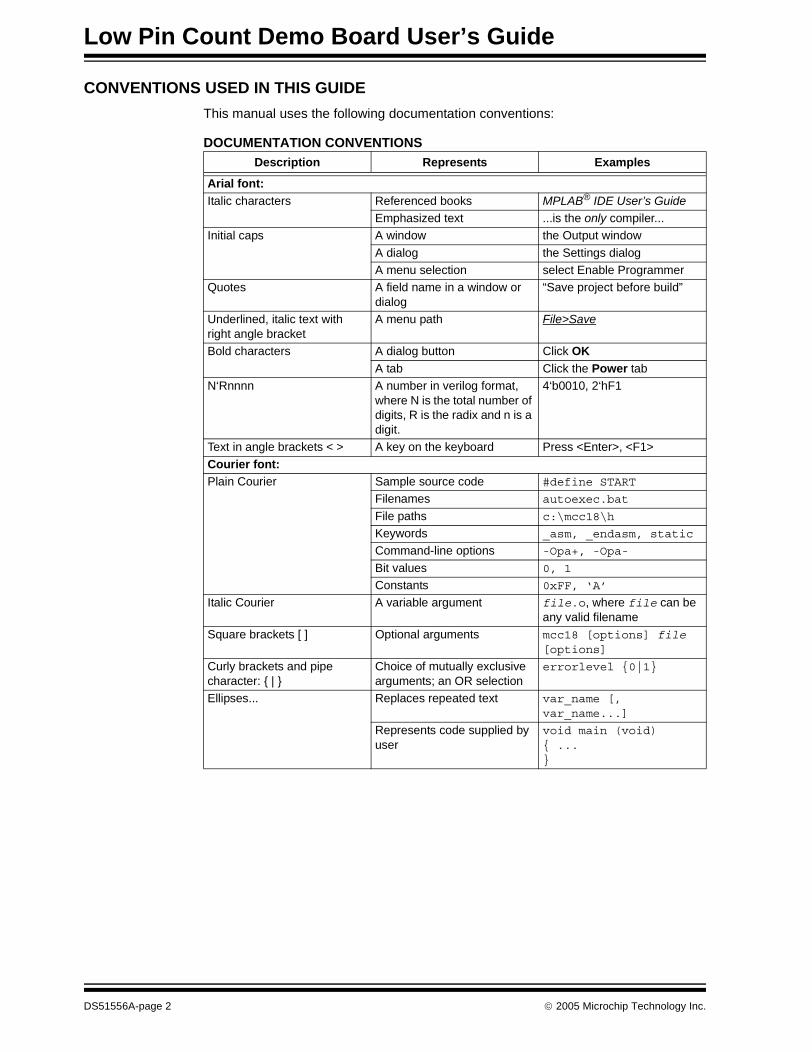
CONVENTIONS USED IN THIS GUIDE
This manual uses the following documentation conventions:
DOCUMENTATION CONVENTIONSDescription Represents Examples
Arial font:Italic characters Referenced books MPLAB® IDE User’s Guide
Emphasized text ...is the only compiler...Initial caps A window the Output window
A dialog the Settings dialogA menu selection select Enable Programmer
Quotes A field name in a window or dialog
“Save project before build”
Underlined, italic text with right angle bracket
A menu path File>Save
Bold characters A dialog button Click OKA tab Click the Power tab
N‘Rnnnn A number in verilog format, where N is the total number of digits, R is the radix and n is a digit.
4‘b0010, 2‘hF1
Text in angle brackets < > A key on the keyboard Press <Enter>, <F1>
Courier font:Plain Courier Sample source code #define START
Filenames autoexec.bat
File paths c:\mcc18\h
Keywords _asm, _endasm, static
Command-line options -Opa+, -Opa-
Bit values 0, 1
Constants 0xFF, ‘A’
Italic Courier A variable argument file.o, where file can be any valid filename
Square brackets [ ] Optional arguments mcc18 [options] file [options]
Curly brackets and pipe character: { | }
Choice of mutually exclusive arguments; an OR selection
errorlevel {0|1}
Ellipses... Replaces repeated text var_name [, var_name...]
Represents code supplied by user
void main (void){ ...}
DS51556A-page 2 © 2005 Microchip Technology Inc.
Preface
WARRANTY REGISTRATION
Please complete the enclosed Warranty Registration Card and mail it promptly. Sending in the Warranty Registration Card entitles users to receive new product updates. Interim software releases are available at the Microchip web site.
RECOMMENDED READING
This user’s guide describes how to use the Low Pin Count (LPC) Demo Board. Other useful documents are listed below. The following Microchip documents are available and recommended as supplemental reference resources.
Readme for Low Pin Count (LPC) Demo Board
For the latest information on using the Low Pin Count (LPC) Demo Board, read the “Readme for Low Pin Count Demo Board.txt” file (an ASCII text file) in the PICkit 2 installation directory. The Readme file contains update information and known issues that may not be included in this user’s guide.
Readme Files
For the latest information on using other tools, read the tool-specific Readme files in the Readmes subdirectory of the MPLAB IDE installation directory. The Readme files contain update information and known issues that may not be included in this user’s guide.
PICkit™ 2 Microcontroller Programmer User’s Guide (DS51553)
Consult this document for instructions on how to use the PICkit 2 Microcontroller Programmer hardware and software.
PIC16F685/687/689/690 Data Sheet (DS41262)
Consult this document for information regarding the PIC16F685/687/689/690 20-pin Flash based, 8-bit CMOS Microcontroller device specifications.
MPLAB® IDE, Simulator, Editor User’s Guide (DS51025)
Consult this document for more information pertaining to the installation and features of the MPLAB Integrated Development Environment (IDE) Software.
© 2005 Microchip Technology Inc. DS51556A-page 3
Low Pin Count Demo Board User’s Guide
THE MICROCHIP WEB SITE
Microchip provides online support via our web site at www.microchip.com. This web site is used as a means to make files and information easily available to customers. Accessible by using your favorite Internet browser, the web site contains the following information:
• Product Support – Data sheets and errata, application notes and sample programs, design resources, user’s guides and hardware support documents, latest software releases and archived software
• General Technical Support – Frequently Asked Questions (FAQs), technical support requests, online discussion groups, Microchip consultant program member listing
• Business of Microchip – Product selector and ordering guides, latest Microchip press releases, listing of seminars and events, listings of Microchip sales offices, distributors and factory representatives
DEVELOPMENT SYSTEMS CUSTOMER CHANGE NOTIFICATION SERVICE
Microchip’s customer notification service helps keep customers current on Microchip products. Subscribers will receive e-mail notification whenever there are changes, updates, revisions or errata related to a specified product family or development tool of interest.
To register, access the Microchip web site at www.microchip.com, click on Customer Change Notification and follow the registration instructions.
The Development Systems product group categories are:
• Compilers – The latest information on Microchip C compilers and other language tools. These include the MPLAB C18 and MPLAB C30 C compilers; MPASM™ and MPLAB ASM30 assemblers; MPLINK™ and MPLAB LINK30 object linkers; and MPLIB™ and MPLAB LIB30 object librarians.
• Emulators – The latest information on Microchip in-circuit emulators.This includes the MPLAB ICE 2000 and MPLAB ICE 4000.
• In-Circuit Debuggers – The latest information on the Microchip in-circuit debugger, MPLAB ICD 2.
• MPLAB® IDE – The latest information on Microchip MPLAB IDE, the Windows® Integrated Development Environment for development systems tools. This list is focused on the MPLAB IDE, MPLAB SIM simulator, MPLAB IDE Project Manager and general editing and debugging features.
• Programmers – The latest information on Microchip programmers. These include the MPLAB PM3 and PRO MATE® II device programmers and the PICSTART® Plus and PICkit® 1 development programmers.
DS51556A-page 4 © 2005 Microchip Technology Inc.
Preface
CUSTOMER SUPPORT
Users of Microchip products can receive assistance through several channels:
• Distributor or Representative• Local Sales Office• Field Application Engineer (FAE)• Technical Support• Development Systems Information Line
Customers should contact their distributor, representative or field application engineer (FAE) for support. Local sales offices are also available to help customers. A listing of sales offices and locations is included in the back of this document.
Technical support is available through the web site at: http://support.microchip.com
In addition, there is a Development Systems Information Line which lists the latest ver-sions of Microchip’s development systems software products. This line also provides information on how customers can receive currently available upgrade kits.
The Development Systems Information Line numbers are:
1-800-755-2345 – United States and most of Canada
1-480-792-7302 – Other International Locations
DOCUMENT REVISION HISTORY
Revision A (May 2005)
• Initial Release of this Document.
© 2005 Microchip Technology Inc. DS51556A-page 5

Low Pin Count Demo Board User’s Guide
NOTES:
DS51556A-page 6 © 2005 Microchip Technology Inc.
LOW PIN COUNT DEMO BOARDUSER’S GUIDE
Chapter 1. Low Pin Count (LPC) Demo Board Overview
1.1 INTRODUCTION
This chapter introduces the Low Pin Count (LPC) Demo Board and describes the LPC Demo Board features.
1.2 HIGHLIGHTS
This chapter discusses:
• Devices supported by the LPC Demo Board• The LPC Demo Board Overview• Running the PICkit™ 2 Starter Kit Default Demonstration
1.3 DEVICES SUPPORTED BY THE LPC DEMO BOARD
For a list of supported devices, see the LPC Demo Board README file on the PICkit™ 2 Starter Kit CD-ROM.
8-pin DIP Flash Devices:
14-pin DIP Flash Devices:
20-pin DIP Flash Devices:
PIC12F508 PIC12F629 PIC12F635PIC12F509 PIC12F675 PIC12F683PIC12F510
PIC16F505 PIC16F630 PIC16F684PIC16F506 PIC16F676 PIC16F688
PIC16F685 PIC16F689 PIC16F785PIC16F687 PIC16F690
© 2005 Microchip Technology Inc. DS51556A-page 7
Low Pin Count Demo Board User’s Guide
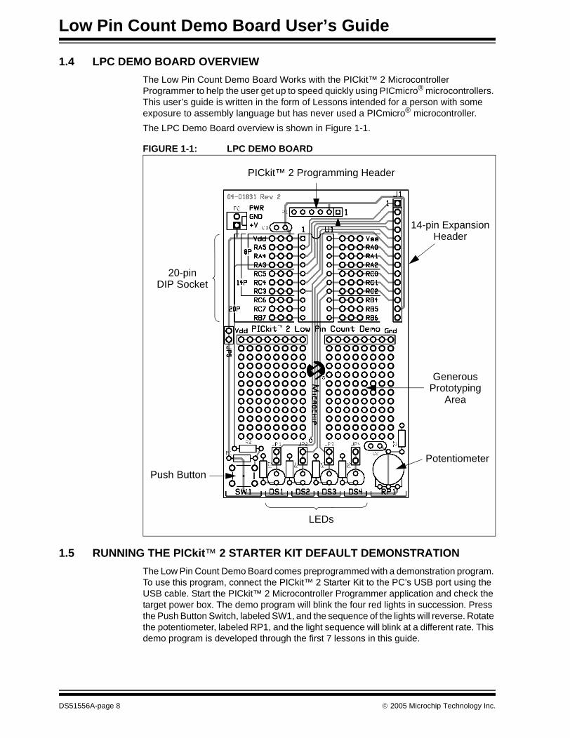
1.4 LPC DEMO BOARD OVERVIEW
The Low Pin Count Demo Board Works with the PICkit™ 2 Microcontroller Programmer to help the user get up to speed quickly using PICmicro® microcontrollers. This user’s guide is written in the form of Lessons intended for a person with some exposure to assembly language but has never used a PICmicro® microcontroller.
The LPC Demo Board overview is shown in Figure 1-1.
FIGURE 1-1: LPC DEMO BOARD
1.5 RUNNING THE PICkit™ 2 STARTER KIT DEFAULT DEMONSTRATION
The Low Pin Count Demo Board comes preprogrammed with a demonstration program. To use this program, connect the PICkit™ 2 Starter Kit to the PC’s USB port using the USB cable. Start the PICkit™ 2 Microcontroller Programmer application and check the target power box. The demo program will blink the four red lights in succession. Press the Push Button Switch, labeled SW1, and the sequence of the lights will reverse. Rotate the potentiometer, labeled RP1, and the light sequence will blink at a different rate. This demo program is developed through the first 7 lessons in this guide.
14-pin Expansion
Generous
Push Button
20-pin
Potentiometer
LEDs
PICkit™ 2 Programming Header
Header
PrototypingArea
DIP Socket
DS51556A-page 8 © 2005 Microchip Technology Inc.
LOW PIN COUNT DEMO BOARDUSER’S GUIDE
Chapter 2. Mid-Range PICmicro® Architectural Overview
2.1 INTRODUCTION
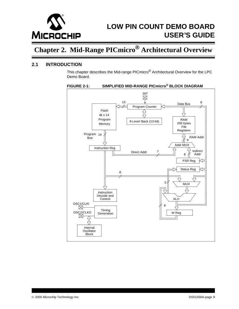
This chapter describes the Mid-range PICmicro® Architectural Overview for the LPC Demo Board.
FIGURE 2-1: SIMPLIFIED MID-RANGE PICmicro® BLOCK DIAGRAM
Flash
ProgramMemory
13 Data Bus 8
14ProgramBus
Instruction Reg
Program Counter
RAM
FileRegisters
Direct Addr 7
RAM Addr9
Addr MUX
IndirectAddr
FSR Reg
Status Reg
MUX
ALU
W Reg
InstructionDecode and
Control
TimingGeneration
OSC1/CLKI
OSC2/CLKO
8
8
8
3
8-Level Stack (13-bit)256 bytes
4k x 14
INT
InternalOscillator
Block
© 2005 Microchip Technology Inc. DS51556A-page 9
Low Pin Count Demo Board User’s Guide
2.2 MEMORY ORGANIZATION
PICmicro® microcontrollers are designed with separate program and data memory areas. This allows faster execution as the address and data busses are separate and do not have to do double duty.
Data Memory is held in file registers. Instructions referring to file registers use 7 bits, so only 128 file registers can be addressed. Multiple file registers are arranged into “pages”. Two extra bits RP0 and RP1 (in the Status register) allow accessing multiple pages. These two bits effectively become the top two bits of the file register address. The additional pages may or may not be implemented, depending on the device.
Mid-range devices reserve the first 32 addresses of each page for Special Function Registers (SFRs). SFRs are how the program interacts with the peripherals. The controls and data registers are memory mapped into the SFR space. Addresses above 0x20 to the end of each page are General Purpose Registers (GPRs), where program variables may be stored.
Some frequently used registers may be accessed from any bank. For example, the Status register is always available no matter which bank is selected via the RP bits. The last 16 bytes (0x70-0x7F) may also be accessed from any bank.
Program Memory is accessed via a 13-bit Program Counter (PC). The lower 8 bits are accessible via SFR (PCL), and the upper 5 are at a PCLATH. See the PIC16F685/687/689/690 Data Sheet’s (DS41262) Section on PCL and PCLATH for more details on the PC. PCLATH becomes important when program memory size exceeds 1k instructions, and also for the table look-up in Lesson 12.
Mid-range PICmicro® MCUs may be clocked by a number of different devices. Unless otherwise noted, the lessons in this manual use the Internal Oscillator running at 4 MHz.
2.3 INSTRUCTION FORMATS
Most instructions follow one of three formats: Byte oriented instructions, Bit oriented instructions and Literal instructions.
Byte instructions contain 7-bit data address, a destination bit, and 6-bit op code. The data address plus the RP0 and RP1 bits create a 9-bit data memory address for one operand. The other operand is the Working register (called W or Wreg). After the instruction executes, the destination bit (d) specifies whether the result will be stored in W or back in the original file register. For example:
ADDWF data,f
adds the contents of Wreg and data, with the result going back into data.
Bit instructions operate on a specific bit within a file register. They contain 7 bits of data address, 3-bit number and the remaining 4 bits are op code. These instructions may set or clear a specific bit within a file register. They may also be used to test a specific bit within a file register. For example:
BSF STATUS,RP0
set the RP0 bit in the Status register.
Literal instructions contain the data operand within the instruction. The Wreg becomes the other operand. Calls and GOTO’s use 11 bits as a literal address.
MOVLW'A'
Moves the ASCII value of ‘A’ (0x41) into Wreg.
DS51556A-page 10 © 2005 Microchip Technology Inc.
Mid-Range PICmicro® Architectural Overview
2.3.1 Assembler Basics
Numbers in the Assembler
Unless otherwise specified, the assembler assumes any numeric constants in the program are hexadecimal (base 16). Binary (base 2), Octal (base 8), Decimal (base 10), and ASCII coding are also supported.
Hexadecimal: 12 or 0x12 or H'12'
Decimal .12 or D'12'
Octal O'12'
Binary B'00010010'
ASCII A'c' or 'c'
Org (Origin)
Org tells the Assembler where to start generating code. Normally we start coding at address ‘0000’, but it could be anywhere. Baseline devices have a Reset vector at the last location in program memory, so it’s good practice to have a GOTO instruction pointing to the beginning of the program.
End
End tells the assembler to stop assembling. There must be one at the end of the program. It does not necessarily have to be at the end of the file, but nothing after the end statement will be assembled.
Defining Data Memory Locations
There are three ways to name a location (see Example 2-1).
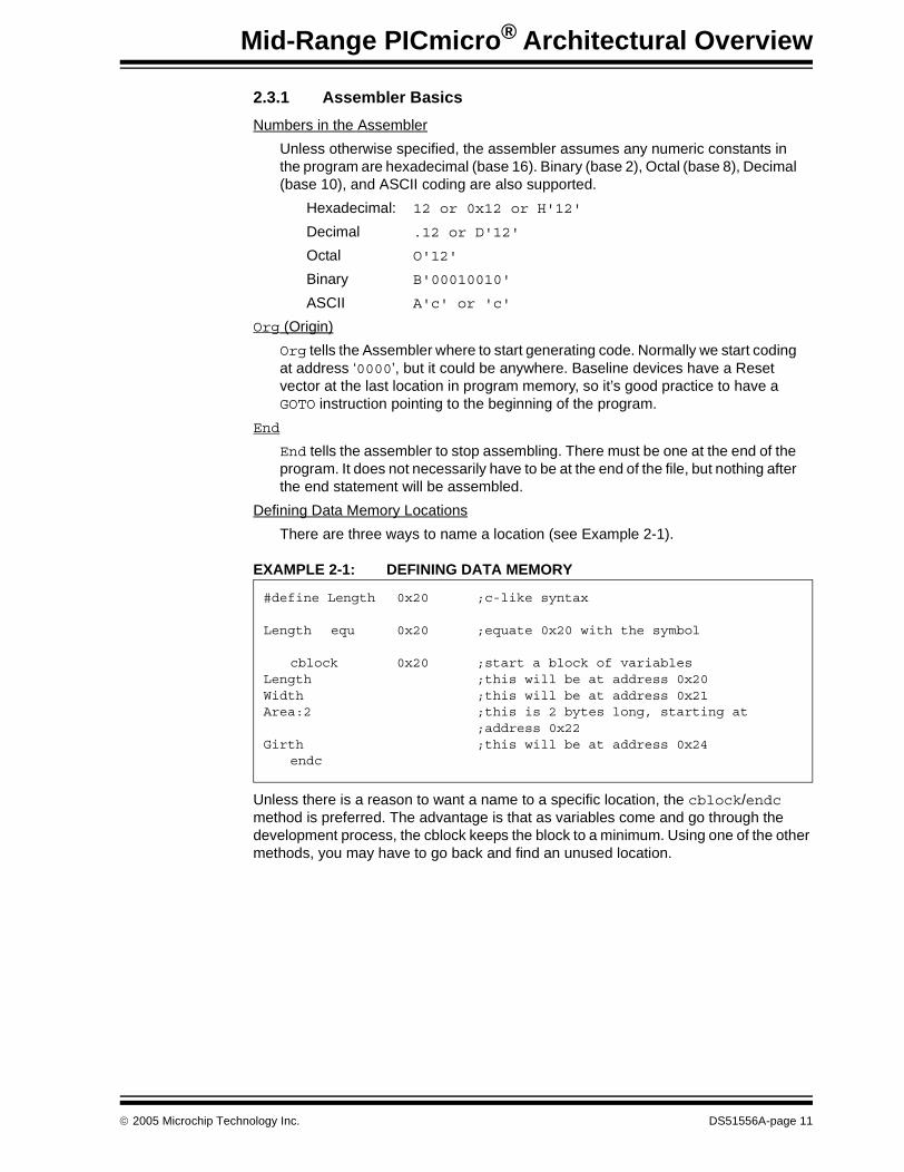
EXAMPLE 2-1: DEFINING DATA MEMORY
Unless there is a reason to want a name to a specific location, the cblock/endc method is preferred. The advantage is that as variables come and go through the development process, the cblock keeps the block to a minimum. Using one of the other methods, you may have to go back and find an unused location.
#define Length 0x20 ;c-like syntax
Length equ 0x20 ;equate 0x20 with the symbol
cblock 0x20 ;start a block of variablesLength ;this will be at address 0x20Width ;this will be at address 0x21Area:2 ;this is 2 bytes long, starting at
;address 0x22Girth ;this will be at address 0x24
endc
© 2005 Microchip Technology Inc. DS51556A-page 11

Low Pin Count Demo Board User’s Guide
NOTES:
DS51556A-page 12 © 2005 Microchip Technology Inc.
LOW PIN COUNT DEMO BOARDUSER’S GUIDE
Chapter 3. LPC Demo Board Lessons
3.1 INTRODUCTION
The following lessons cover basic LPC Demo Board features. Refer to applicable documents as needed. Any updates to the applicable documents are available on Microchip’s web site.
The code and hex files are installed in C:\Microchip\PICkit 2 Lessons\. They may also be found on the PICkit™ 2 CD-ROM under directory \PICkit 2 Lessons\.
3.2 LPC DEMO BOARD LESSONS
• Lesson 1: Hello World (Light a LED)• Lesson 2: Delay Loop (Blink a LED)• Lesson 3: Rotate (Move the LED)• Lesson 4: Analog-to-Digital• Lesson 5: Variable Speed Rotate• Lesson 6: Switch Debounce• Lesson 7: Reversible Variable Speed Rotate• Lesson 8: Function Calls• Lesson 9: Timer0• Lesson 10: Interrupts• Lesson 11: Indirect Data Addressing• Lesson 12: Look-up Table (ROM Array)
© 2005 Microchip Technology Inc. DS51556A-page 13
Low Pin Count Demo Board User’s Guide
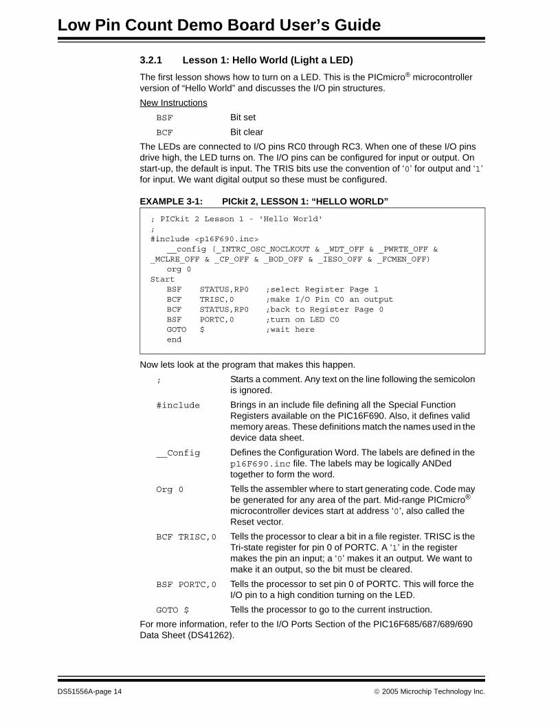
3.2.1 Lesson 1: Hello World (Light a LED)
The first lesson shows how to turn on a LED. This is the PICmicro® microcontroller version of “Hello World” and discusses the I/O pin structures.
New Instructions
BSF Bit set
BCF Bit clear
The LEDs are connected to I/O pins RC0 through RC3. When one of these I/O pins drive high, the LED turns on. The I/O pins can be configured for input or output. On start-up, the default is input. The TRIS bits use the convention of ‘0’ for output and ‘1’ for input. We want digital output so these must be configured.
EXAMPLE 3-1: PICkit 2, LESSON 1: “HELLO WORLD”
Now lets look at the program that makes this happen.
; Starts a comment. Any text on the line following the semicolon is ignored.
#include Brings in an include file defining all the Special Function Registers available on the PIC16F690. Also, it defines valid memory areas. These definitions match the names used in the device data sheet.
__Config Defines the Configuration Word. The labels are defined in the p16F690.inc file. The labels may be logically ANDed together to form the word.
Org 0 Tells the assembler where to start generating code. Code may be generated for any area of the part. Mid-range PICmicro® microcontroller devices start at address ‘0’, also called the Reset vector.
BCF TRISC,0 Tells the processor to clear a bit in a file register. TRISC is the Tri-state register for pin 0 of PORTC. A ‘1’ in the register makes the pin an input; a ‘0’ makes it an output. We want to make it an output, so the bit must be cleared.
BSF PORTC,0 Tells the processor to set pin 0 of PORTC. This will force the I/O pin to a high condition turning on the LED.
GOTO $ Tells the processor to go to the current instruction.
For more information, refer to the I/O Ports Section of the PIC16F685/687/689/690 Data Sheet (DS41262).
; PICkit 2 Lesson 1 - 'Hello World';#include <p16F690.inc>
__config (_INTRC_OSC_NOCLKOUT & _WDT_OFF & _PWRTE_OFF & _MCLRE_OFF & _CP_OFF & _BOD_OFF & _IESO_OFF & _FCMEN_OFF)
org 0Start
BSF STATUS,RP0 ;select Register Page 1BCF TRISC,0 ;make I/O Pin C0 an outputBCF STATUS,RP0 ;back to Register Page 0BSF PORTC,0 ;turn on LED C0GOTO $ ;wait hereend
DS51556A-page 14 © 2005 Microchip Technology Inc.
LPC Demo Board Lessons
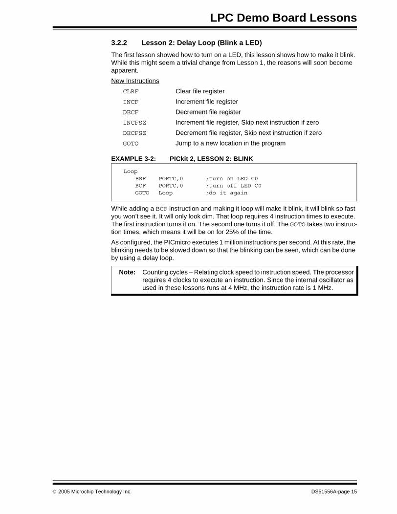
3.2.2 Lesson 2: Delay Loop (Blink a LED)
The first lesson showed how to turn on a LED, this lesson shows how to make it blink. While this might seem a trivial change from Lesson 1, the reasons will soon become apparent.
New Instructions
CLRF Clear file register
INCF Increment file register
DECF Decrement file register
INCFSZ Increment file register, Skip next instruction if zero
DECFSZ Decrement file register, Skip next instruction if zero
GOTO Jump to a new location in the program
EXAMPLE 3-2: PICkit 2, LESSON 2: BLINK
While adding a BCF instruction and making it loop will make it blink, it will blink so fast you won’t see it. It will only look dim. That loop requires 4 instruction times to execute. The first instruction turns it on. The second one turns it off. The GOTO takes two instruc-tion times, which means it will be on for 25% of the time.
As configured, the PICmicro executes 1 million instructions per second. At this rate, the blinking needs to be slowed down so that the blinking can be seen, which can be done by using a delay loop.
LoopBSF PORTC,0 ;turn on LED C0BCF PORTC,0 ;turn off LED C0GOTO Loop ;do it again
Note: Counting cycles – Relating clock speed to instruction speed. The processor requires 4 clocks to execute an instruction. Since the internal oscillator as used in these lessons runs at 4 MHz, the instruction rate is 1 MHz.
© 2005 Microchip Technology Inc. DS51556A-page 15
Low Pin Count Demo Board User’s Guide
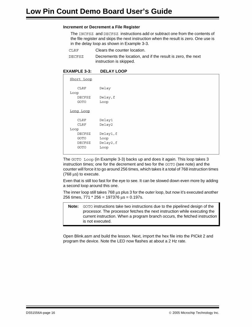
Increment or Decrement a File Register
The INCFSZ and DECFSZ instructions add or subtract one from the contents of the file register and skips the next instruction when the result is zero. One use is in the delay loop as shown in Example 3-3.
CLRF Clears the counter location.
DECFSZ Decrements the location, and if the result is zero, the next instruction is skipped.
EXAMPLE 3-3: DELAY LOOP
The GOTO Loop (in Example 3-3) backs up and does it again. This loop takes 3 instruction times; one for the decrement and two for the GOTO (see note) and the counter will force it to go around 256 times, which takes it a total of 768 instruction times (768 μs) to execute.
Even that is still too fast for the eye to see. It can be slowed down even more by adding a second loop around this one.
The inner loop still takes 768 μs plus 3 for the outer loop, but now it’s executed another 256 times, 771 * 256 = 197376 μs = 0.197s.
Open Blink.asm and build the lesson. Next, import the hex file into the PICkit 2 and program the device. Note the LED now flashes at about a 2 Hz rate.
Short Loop
CLRF DelayLoop
DECFSZ Delay,fGOTO Loop
Long Loop
CLRF Delay1CLRF Delay2
LoopDECFSZ Delay1,fGOTO LoopDECFSZ Delay2,fGOTO Loop
Note: GOTO instructions take two instructions due to the pipelined design of the processor. The processor fetches the next instruction while executing the current instruction. When a program branch occurs, the fetched instruction is not executed.
DS51556A-page 16 © 2005 Microchip Technology Inc.
LPC Demo Board Lessons
3.2.3 Lesson 3: Rotate (Move the LED)
Building on Lessons 1 and 2, which showed how to light up a LED and then make it blink with a delay loop, this lesson adds rotation. It will light up DS4 and then shift it to DS3, then DS2, then DS1 and back to DS4.
New Instructions
MOVLW Loads Wreg with a literal value
MOVWF Moves the contents of Wreg to a file register
MOVF Moves the contents of a file register, either to Wreg or back into the file register (see note)
RRF Rotate file register right
RLF Rotate file register left
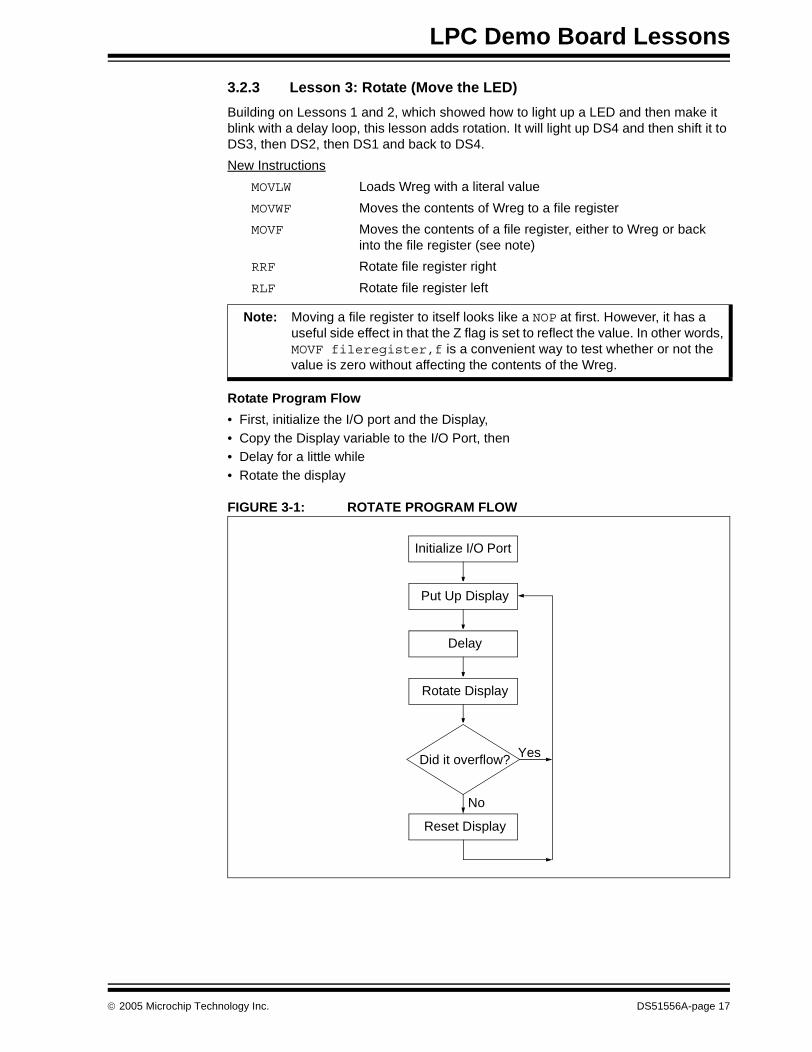
Rotate Program Flow
• First, initialize the I/O port and the Display,• Copy the Display variable to the I/O Port, then• Delay for a little while• Rotate the display
FIGURE 3-1: ROTATE PROGRAM FLOW
Note: Moving a file register to itself looks like a NOP at first. However, it has a useful side effect in that the Z flag is set to reflect the value. In other words, MOVF fileregister,f is a convenient way to test whether or not the value is zero without affecting the contents of the Wreg.
Initialize I/O Port
Put Up Display
Delay
Rotate Display
Reset Display
Did it overflow?
No
Yes
© 2005 Microchip Technology Inc. DS51556A-page 17
Low Pin Count Demo Board User’s Guide
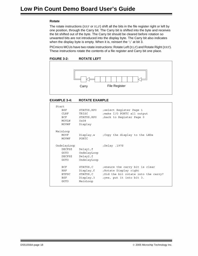
Rotate
The rotate instructions (RRF or RLF) shift all the bits in the file register right or left by one position, through the Carry bit. The Carry bit is shifted into the byte and receives the bit shifted out of the byte. The Carry bit should be cleared before rotation so unwanted bits are not introduced into the display byte. The Carry bit also indicates when the display byte is empty. When it is, reinsert the ‘1’ at bit 3.
PICmicro MCUs have two rotate instructions: Rotate Left (RLF) and Rotate Right (RRF). These instructions rotate the contents of a file register and Carry bit one place.
FIGURE 3-2: ROTATE LEFT
EXAMPLE 3-4: ROTATE EXAMPLE
File RegisterCarry
StartBSF STATUS,RP0 ;select Register Page 1CLRF TRISC ;make I/O PORTC all outputBCF STATUS,RP0 ;back to Register Page 0MOVLW 0x08MOVWF Display
MainLoopMOVF Display,w ;Copy the display to the LEDsMOVWF PORTC
OndelayLoop ;Delay .197SDECFSZ Delay1,fGOTO OndelayLoopDECFSZ Delay2,fGOTO OndelayLoop
BCF STATUS,C ;ensure the carry bit is clearRRF Display,f ;Rotate Display rightBTFSC STATUS,C ;Did the bit rotate into the carry?BSF Display,3 ;yes, put it into bit 3.GOTO MainLoop
DS51556A-page 18 © 2005 Microchip Technology Inc.
LPC Demo Board Lessons
3.2.4 Lesson 4: Analog-to-Digital
This lesson shows how to configure the ADC, run a conversion, read the analog voltage controlled by the potentiometer (RP1) on the board, and display the high order 4 bits on the display.
The PIC16F690 has an on board Analog-to-Digital Converter (ADC) with 10 bits of resolution on any of 11 channels. The converter can be referenced to the device’s VDD or an external voltage reference. The LPC Demo Board references it to VDD as provided by the USB cable. The answer from the ADC is represented by a ratio of the voltage to the reference.
ADC = V/VREF * 1023
Converting the answer from the ADC back to voltage requires solving for V.
V = ADC/1023 * VREF
Two of the three factors on the right side of the equation are constants and may be calculated in advance. This eliminates the need to actually divide, but still requires fixed or floating point multiply to solve the equation on the fly.
However, sometimes, such as when reading a sensor, calculating the voltage is only the first step. There may be additional math to calculate the meaningful data from the sensor. For example, when reading a thermistor, calculating the voltage is only the first step on the way to getting the temperature.
There are other means to convert ADC values, including a straight table look-up or a piece-wise linear interpolation. Each of these represents different speed/memory trade-offs.
The schematic (Appendix A. “Hardware Schematics”) shows the wiper on the potentiometer is connected to pin RA0 on the PIC16F690.
Here’s the checklist for this lesson:
• Configure PORTA as an analog input, TRISA<0> = 1, ANSEL<0> = 1• Select clock scaling in ADCON1.• Select channel, justification and VREF source in ADCON0.
© 2005 Microchip Technology Inc. DS51556A-page 19
Low Pin Count Demo Board User’s Guide
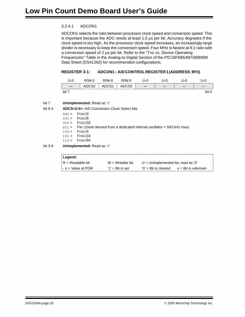
3.2.4.1 ADCON1
ADCON1 selects the ratio between processor clock speed and conversion speed. This is important because the ADC needs at least 1.6 μs per bit. Accuracy degrades if the clock speed is too high. As the processor clock speed increases, an increasingly large divider is necessary to keep the conversion speed. Four MHz is fastest at 8:1 ratio with a conversion speed of 2 μs per bit. Refer to the “TAD vs. Device Operating Frequencies” Table in the Analog-to-Digital Section of the PIC16F685/687/689/690 Data Sheet (DS41262) for recommended configurations.
REGISTER 3-1: ADCON1 – A/D CONTROL REGISTER 1 (ADDRESS: 9Fh)
U-0 R/W-0 R/W-0 R/W-0 U-0 U-0 U-0 U-0
— ADCS2 ADCS1 ADCS0 — — — —
bit 7 bit 0
bit 7 Unimplemented: Read as ‘0’
bit 6-4 ADCS<2:0>: A/D Conversion Clock Select bits000 = FOSC/2001 = FOSC/8010 = FOSC/32x11 = FRC (clock derived from a dedicated internal oscillator = 500 kHz max)100 = FOSC/4101 = FOSC/16110 = FOSC/64
bit 3-0 Unimplemented: Read as ‘0’
Legend:
R = Readable bit W = Writable bit U = Unimplemented bit, read as ‘0’
- n = Value at POR ‘1’ = Bit is set ‘0’ = Bit is cleared x = Bit is unknown
DS51556A-page 20 © 2005 Microchip Technology Inc.
LPC Demo Board Lessons
3.2.4.2 ADCON0
ADCON0 controls the ADC operation. Bit 0 turns on the ADC module. Bit 1 starts a conversion and bits <5:2> selects which channel the ADC will operate. VCFG bit< 6> selects the ADC reference, which may be either VDD or a separate reference voltage on VREF. ADFM bit <7> selects whether the 10 bits are right or left justified in the 16 bits.
For purposes of this lesson, the ADC must be turned on and pointed to RA0. Choose the internal voltage reference and 8TOSC conversion clock.
The ADC needs about 5 μs, after changing channels, to allow the ADC sampling capacitor to settle. Finally, we can start the conversion by setting the GO bit in ADCON0. The bit also serves as the DONE flag. That is, the ADC will clear the same bit when the conversion is complete. The answer is then available in ADRESH:ADRESL.
This lesson takes the high order 4 bits of the result and copies them to the display LEDs attached to PORTC.
See the Analog-to-Digital section in the PIC16F685/687/689/690 Data Sheet (DS41262) for more details on the ADC module.
REGISTER 3-2: ADCON0 – A/D CONTROL REGISTER (ADDRESS: 1Fh)
R/W-0 R/W-0 R/W-0 R/W-0 R/W-0 R/W-0 R/W-0 R/W-0
ADFM VCFG CHS3 CHS2 CHS1 CHS0 GO/DONE ADON
bit 7 bit 0
bit 7 ADFM: A/D Result Formed Select bit1 = Right justified0 = Left justified
bit 6 VCFG: Voltage Reference bit1 = VREF pin0 = VDD
bit 5-2 CHS<3:0>: Analog Channel Select bits0000 = Channel 00 (AN0)0001 = Channel 01 (AN1)0010 = Channel 02 (AN2)0011 = Channel 03 (AN3)0100 = Channel 04 (AN4)0101 = Channel 05 (AN5)0110 = Channel 06 (AN6)0111 = Channel 07 (AN7)1000 = Channel 08 (AN8)1001 = Channel 09 (AN9)1010 = Channel 10 (AN10)1011 = Channel 11 (AN11)1100 = CVREF
1101 = VP61110 = Reserved. Do not use.1111 = Reserved. Do not use.
bit 1 GO/DONE: A/D Conversion Status bit1 = A/D conversion cycle in progress. Setting this bit starts an A/D conversion cycle. This bit is automatically cleared by hardware when the A/D conversion has completed.0 = A/D conversion completed/not in progress
bit 0 ADON: A/D Enable bit1 = A/D converter module is enabled0 = A/D converter is shut off and consumes no operating current
Legend:
R = Readable bit W = Writable bit U = Unimplemented bit, read as ‘0’
- n = Value at POR ‘1’ = Bit is set ‘0’ = Bit is cleared x = Bit is unknown
© 2005 Microchip Technology Inc. DS51556A-page 21
Low Pin Count Demo Board User’s Guide
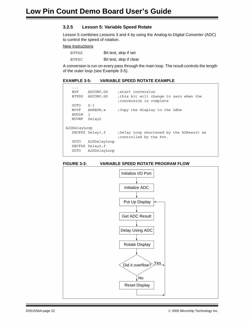
3.2.5 Lesson 5: Variable Speed Rotate
Lesson 5 combines Lessons 3 and 4 by using the Analog-to-Digital Converter (ADC) to control the speed of rotation.
New Instructions
BTFSS Bit test, skip if set
BTFSC Bit test, skip if clear
A conversion is run on every pass through the main loop. The result controls the length of the outer loop (see Example 3-5).
EXAMPLE 3-5: VARIABLE SPEED ROTATE EXAMPLE
FIGURE 3-3: VARIABLE SPEED ROTATE PROGRAM FLOW
...BSF ADCON0,GO ;start conversionBTFSS ADCON0,GO ;this bit will change to zero when the
;conversion is completeGOTO $-1MOVF ADRESH,w ;Copy the display to the LEDsADDLW 1MOVWF Delay2
A2DDelayLoopDECFSZ Delay1,f ;Delay Loop shortened by the ADResult as
;controlled by the Pot. GOTO A2DDelayLoopDECFSZ Delay2,fGOTO A2DDelayLoop
Initialize I/O Port
Put Up Display
Delay Using ADC
Rotate Display
Reset Display
Did it overflow?
No
Yes
Initialize ADC
Get ADC Result
DS51556A-page 22 © 2005 Microchip Technology Inc.
LPC Demo Board Lessons
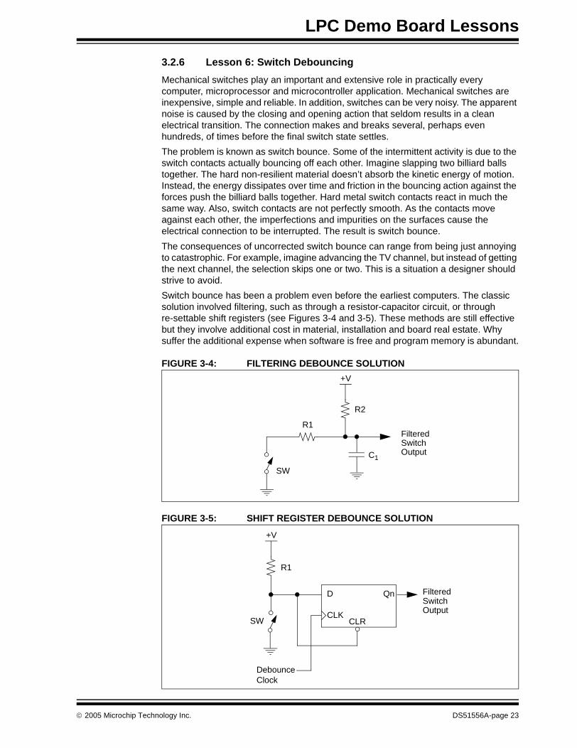
3.2.6 Lesson 6: Switch Debouncing
Mechanical switches play an important and extensive role in practically every computer, microprocessor and microcontroller application. Mechanical switches are inexpensive, simple and reliable. In addition, switches can be very noisy. The apparent noise is caused by the closing and opening action that seldom results in a clean electrical transition. The connection makes and breaks several, perhaps even hundreds, of times before the final switch state settles.
The problem is known as switch bounce. Some of the intermittent activity is due to the switch contacts actually bouncing off each other. Imagine slapping two billiard balls together. The hard non-resilient material doesn’t absorb the kinetic energy of motion. Instead, the energy dissipates over time and friction in the bouncing action against the forces push the billiard balls together. Hard metal switch contacts react in much the same way. Also, switch contacts are not perfectly smooth. As the contacts move against each other, the imperfections and impurities on the surfaces cause the electrical connection to be interrupted. The result is switch bounce.
The consequences of uncorrected switch bounce can range from being just annoying to catastrophic. For example, imagine advancing the TV channel, but instead of getting the next channel, the selection skips one or two. This is a situation a designer should strive to avoid.
Switch bounce has been a problem even before the earliest computers. The classic solution involved filtering, such as through a resistor-capacitor circuit, or through re-settable shift registers (see Figures 3-4 and 3-5). These methods are still effective but they involve additional cost in material, installation and board real estate. Why suffer the additional expense when software is free and program memory is abundant.
FIGURE 3-4: FILTERING DEBOUNCE SOLUTION
FIGURE 3-5: SHIFT REGISTER DEBOUNCE SOLUTION
+V
R1
R2
Filtered Switch Output
SW
C1
+V
R1
Filtered Switch Output
SW
Debounce Clock
D
CLKCLR
Qn
© 2005 Microchip Technology Inc. DS51556A-page 23
Low Pin Count Demo Board User’s Guide
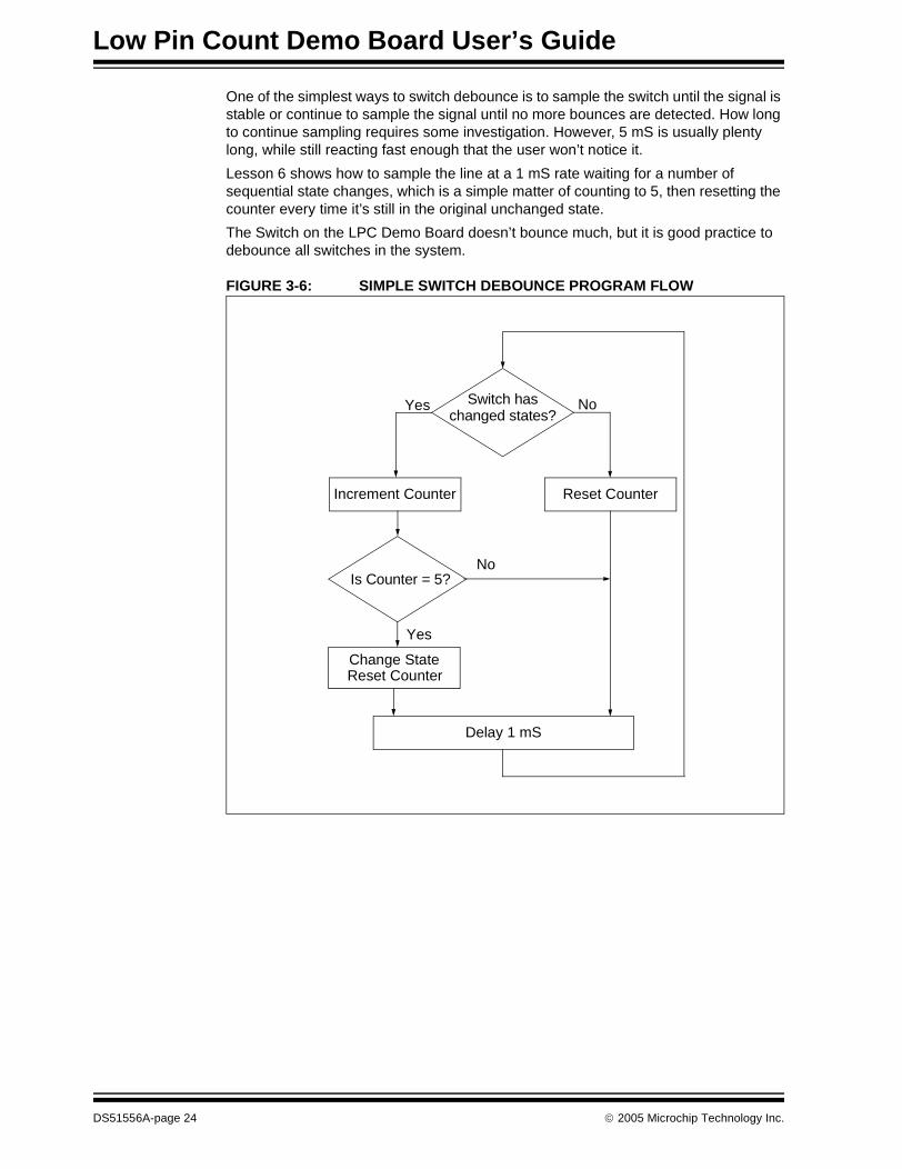
One of the simplest ways to switch debounce is to sample the switch until the signal is stable or continue to sample the signal until no more bounces are detected. How long to continue sampling requires some investigation. However, 5 mS is usually plenty long, while still reacting fast enough that the user won’t notice it.
Lesson 6 shows how to sample the line at a 1 mS rate waiting for a number of sequential state changes, which is a simple matter of counting to 5, then resetting the counter every time it’s still in the original unchanged state.
The Switch on the LPC Demo Board doesn’t bounce much, but it is good practice to debounce all switches in the system.
FIGURE 3-6: SIMPLE SWITCH DEBOUNCE PROGRAM FLOW
Increment Counter
No
No
Reset Counter
Change StateReset Counter
Is Counter = 5?
Switch haschanged states?
Yes
Yes
Delay 1 mS
DS51556A-page 24 © 2005 Microchip Technology Inc.
LPC Demo Board Lessons
3.2.7 Lesson 7: Reversible Variable Speed Rotate
Lesson 7 combines Lessons 5 and 6 using the button to reverse the direction of rotation when the button is pressed and adjusting the potentiometer to control the speed of rotation.
The program needs to keep track of rotation direction and new code needs to be added to rotate in the other direction.
Lesson 5 rotates right and checks for a ‘1’ in the Carry bit to determine when to restart the sequence. In Lesson 7, we’ll also need to rotate left and check for a ‘1’ in bit 4 of the display. When the ‘1’ shows up in bit 4 of the display, re-insert it into the bit 0 position.
EXAMPLE 3-6: REVERSIBLE VARIABLE SPEED ROTATE EXAMPLE
Original Version:
RotateRRF Display,fBTFSC STATUS,C ;Did the bit rotate into the carry?BSF Display,3 ;yes, put it into bit 3.
Bidirectional Version:
RotateBCF STATUS,C ;ensure the carry bit is clearBTFSS Direction,0GOTO RotateLeft
RotateRightRRF Display,fBTFSC STATUS,C ;Did the bit rotate into the carry?BSF Display,3 ;yes, put it into bit 3.GOTO MainLoop
RotateLeftRLF Display,fBTFSC Display,4 ;did it rotate out of the displayBSF Display,0 ;yes, put it into bit 0GOTO MainLoop
© 2005 Microchip Technology Inc. DS51556A-page 25
Low Pin Count Demo Board User’s Guide
3.2.8 Lesson 8: Function Calls
Lesson 8 shows the reversible LEDs but with the Delay Loop rewritten as a function.
New Instructions
CALL Invokes functions or subroutines
RETURN Terminates functions or subroutines
RETLW Terminates functions or subroutines
Functions or Subroutines are invoked with the CALL instruction and terminated with a RETURN or RETLW instruction. RETURN jumps back to the original program at the location following the CALL. RETLW also returns to the calling program, but loads Wreg with a constant.
The mid-range PICmicro MCU device’s CALL stack can hold up to 8 return addresses. If a ninth CALL is made, it will overwrite the first one and then the program will not be able to RETURN all the way back.
Passing Arguments
Arguments to the subroutine may be passed in a number of ways. Wreg is a convenient place to pass one byte and the FSR may be used to pass another byte, if not otherwise used. If more data must be passed, a buffer must be allocated.
When the Delay function is pulled out to a subroutine, the ADC result is moved into Wreg, then the CALL transfers control to the Delay subroutine. The RETURN transfers control to the MOVLW following the CALL.
EXAMPLE 3-7: FUNCTION CALL EXAMPLE
MOVF ADRESH,wCALL Delay ;call delay function
;returns here when done...GOTO xxx
; Delay function. ; Delay time is Wreg value * 771 uSDelay
MOVWF Delay2DelayLoop
DECFSZ Delay1,fGOTO DelayLoopDECFSZ Delay2,fGOTO DelayLoopRETURN
DS51556A-page 26 © 2005 Microchip Technology Inc.
LPC Demo Board Lessons
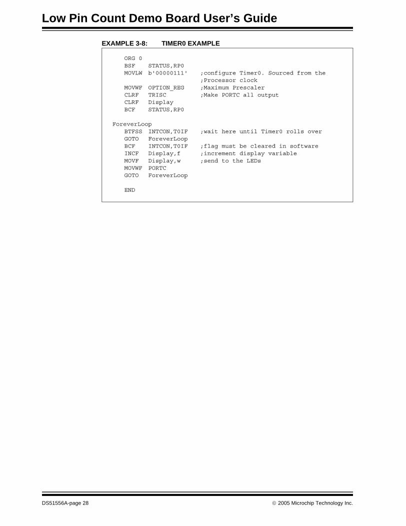
3.2.9 Lesson 9: Timer0
Timer0 is a counter implemented in the processor. It may be used to count processor clock cycles or external events. Lesson 9 configures it to count instruction cycles and set a flag when it rolls over. This frees up the processor to do meaningful work rather than just wasting cycles.
Timer0 is an 8-bit counter with an optional prescaler, which is configured to divide by 256 before reaching the Timer0 counter.
FIGURE 3-7: TIMER0 SIMPLIFIED
TMR0 is a Special Function Register (SFR) and may be read or modified by the program. The Prescaler is not a SFR and thus cannot be read or modified by the program. However, writing to TMR0 clears the Prescaler.
The timer may be fed either by the same clock that drives the processor or by an external event. Driven by the processor clock, it increments once for every instruction cycle. This is a convenient method of marking time, better than delay loops, as it allows the processor to work on the problem rather than waste cycles in delay loops.
The prescaler is configured through the OPTION_REG, see Figure 3-8.
FIGURE 3-8: PRESCALER CONFIGURATION THROUGH OPTION_REG
Lesson 9 configures Timer0 with the Prescaler for a maximum delay on Timer0. The prescaler will divide the processor clock by 256 and Timer0 will divide that by 256 again. Thus, Timer0 Flag will be set every 65536 μs (0.0000001 second * 256 * 256), or about 15 times a second. The main program sits in a loop waiting for the rollover and when it does, it increments the display and then loops back.
Prescaler T0IFTMR0Clock/4 or
T0CKI pin
Prescaler may be configuredto divide by 2, 4, 8, 16, 32, 64, 128 or 256.
Flag set when
Must be cleared TMR0 overflows.
in software.
Note: See PIC16F690 Timer0 section for more details.
X X T0CS T0SE PSA PS2 PS1 PS0
bit 7 bit 0
Legend:
X: Don’t cares – not Timer0 related.
T0CS: Timer0 Clock Source 0 for Instruction Clock.
T0SE: Timer0 Source Edge – Don’t care when connected to instruction clock.
PSA: Prescaler Assignment 0 assigns to Timer0.
PS: Prescaler rate select ‘111’ – full prescaler, divide by 256.
© 2005 Microchip Technology Inc. DS51556A-page 27
Low Pin Count Demo Board User’s Guide
EXAMPLE 3-8: TIMER0 EXAMPLE
ORG 0BSF STATUS,RP0MOVLW b'00000111' ;configure Timer0. Sourced from the
;Processor clockMOVWF OPTION_REG ;Maximum PrescalerCLRF TRISC ;Make PORTC all outputCLRF DisplayBCF STATUS,RP0
ForeverLoopBTFSS INTCON,T0IF ;wait here until Timer0 rolls overGOTO ForeverLoopBCF INTCON,T0IF ;flag must be cleared in softwareINCF Display,f ;increment display variableMOVF Display,w ;send to the LEDsMOVWF PORTCGOTO ForeverLoop
END
DS51556A-page 28 © 2005 Microchip Technology Inc.
LPC Demo Board Lessons
3.2.10 Lesson 10: Interrupts
New Instructions
RETFIE Return from Interrupt
SWAPF Swap nibbles in file register
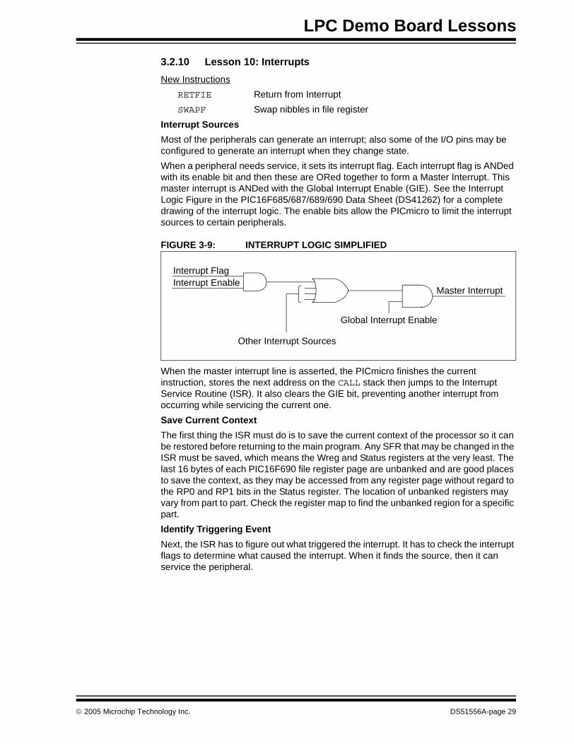
Interrupt Sources
Most of the peripherals can generate an interrupt; also some of the I/O pins may be configured to generate an interrupt when they change state.
When a peripheral needs service, it sets its interrupt flag. Each interrupt flag is ANDed with its enable bit and then these are ORed together to form a Master Interrupt. This master interrupt is ANDed with the Global Interrupt Enable (GIE). See the Interrupt Logic Figure in the PIC16F685/687/689/690 Data Sheet (DS41262) for a complete drawing of the interrupt logic. The enable bits allow the PICmicro to limit the interrupt sources to certain peripherals.
FIGURE 3-9: INTERRUPT LOGIC SIMPLIFIED
When the master interrupt line is asserted, the PICmicro finishes the current instruction, stores the next address on the CALL stack then jumps to the Interrupt Service Routine (ISR). It also clears the GIE bit, preventing another interrupt from occurring while servicing the current one.
Save Current Context
The first thing the ISR must do is to save the current context of the processor so it can be restored before returning to the main program. Any SFR that may be changed in the ISR must be saved, which means the Wreg and Status registers at the very least. The last 16 bytes of each PIC16F690 file register page are unbanked and are good places to save the context, as they may be accessed from any register page without regard to the RP0 and RP1 bits in the Status register. The location of unbanked registers may vary from part to part. Check the register map to find the unbanked region for a specific part.
Identify Triggering Event
Next, the ISR has to figure out what triggered the interrupt. It has to check the interrupt flags to determine what caused the interrupt. When it finds the source, then it can service the peripheral.
Master Interrupt
Global Interrupt Enable
Interrupt FlagInterrupt Enable
Other Interrupt Sources
© 2005 Microchip Technology Inc. DS51556A-page 29
Low Pin Count Demo Board User’s Guide
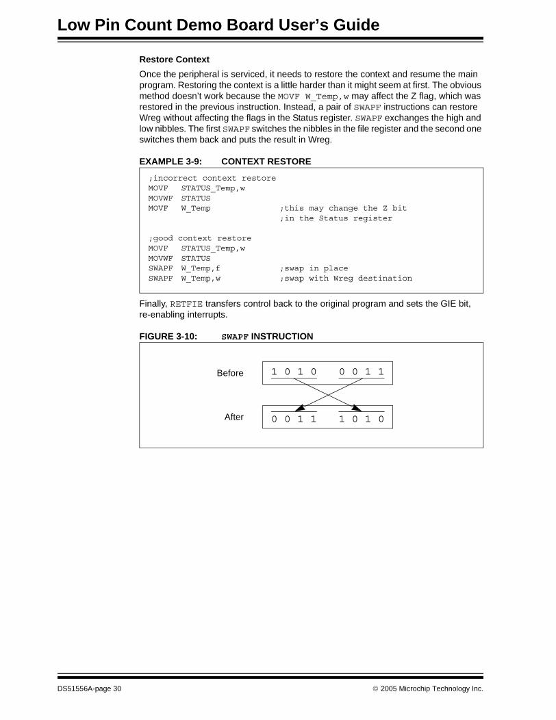
Restore Context
Once the peripheral is serviced, it needs to restore the context and resume the main program. Restoring the context is a little harder than it might seem at first. The obvious method doesn’t work because the MOVF W_Temp,w may affect the Z flag, which was restored in the previous instruction. Instead, a pair of SWAPF instructions can restore Wreg without affecting the flags in the Status register. SWAPF exchanges the high and low nibbles. The first SWAPF switches the nibbles in the file register and the second one switches them back and puts the result in Wreg.
EXAMPLE 3-9: CONTEXT RESTORE
Finally, RETFIE transfers control back to the original program and sets the GIE bit, re-enabling interrupts.
FIGURE 3-10: SWAPF INSTRUCTION
;incorrect context restoreMOVF STATUS_Temp,wMOVWF STATUSMOVF W_Temp ;this may change the Z bit
;in the Status register
;good context restoreMOVF STATUS_Temp,wMOVWF STATUSSWAPF W_Temp,f ;swap in placeSWAPF W_Temp,w ;swap with Wreg destination
Before
After
1 0 1 0 0 0 1 1
1 0 1 00 0 1 1
DS51556A-page 30 © 2005 Microchip Technology Inc.
LPC Demo Board Lessons
3.2.11 Lesson 11: Indirect Data Addressing
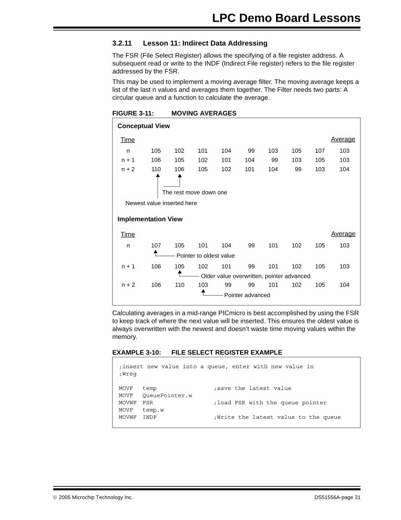
The FSR (File Select Register) allows the specifying of a file register address. A subsequent read or write to the INDF (Indirect File register) refers to the file register addressed by the FSR.
This may be used to implement a moving average filter. The moving average keeps a list of the last n values and averages them together. The Filter needs two parts: A circular queue and a function to calculate the average.
FIGURE 3-11: MOVING AVERAGES
Calculating averages in a mid-range PICmicro is best accomplished by using the FSR to keep track of where the next value will be inserted. This ensures the oldest value is always overwritten with the newest and doesn’t waste time moving values within the memory.
EXAMPLE 3-10: FILE SELECT REGISTER EXAMPLE
Time Average
n 105 102 101 104 99 103 105 107 103
n + 1 106 105 102 101 104 99 103 105 103
n + 2 110 106 105 102 101 104 99 103 104
Newest value inserted here
The rest move down one
Conceptual View
Implementation View
Time Average
n 107 105 101 104 99 101 102 105 103
n + 1 106 105 102 101 99 101 102 105 103
n + 2 106 110 103 99 99 101 102 105 104
Pointer to oldest value
Older value overwritten, pointer advanced
Pointer advanced
;insert new value into a queue, enter with new value in;Wreg
MOVF temp ;save the latest valueMOVF QueuePointer,wMOVWF FSR ;load FSR with the queue pointerMOVF temp,wMOVWF INDF ;Write the latest value to the queue
© 2005 Microchip Technology Inc. DS51556A-page 31
Low Pin Count Demo Board User’s Guide
Lesson 11 adds a Moving Average Filter to the Analog-to-Digital code in Lesson 4. Twisting the potentiometer changes the value read by the Analog-to-Digital. The filtered value is then sent to the LED display. The filter only runs every 0.2 seconds to slow down the display changes and make it visible. The display appears to count from the old potentiometer position to the new position.
The filter averages the last 8 readings. Choosing a power of two for the number of samples allows division by simple rotates instead of longhand.
Rather than summing the array every time, it’s faster to keep a running sum, then subtract out the oldest value in the queue and adding in the new value.
DS51556A-page 32 © 2005 Microchip Technology Inc.
LPC Demo Board Lessons
3.2.12 Lesson 12: Look-up Table (ROM Array)
Lesson 8 introduced function calls. Lesson 12 shows how function calls and calculated modification of the Program Counter may be used to implement a Look-up Table (see Example 3-11).
It is sometimes useful to implement a table to convert from one value to another.
Expressed in a high-level language it might look like this:
y = function(x);
That is for every value of x, it returns the corresponding y value.
Look-up tables are a fast way to convert an input to meaningful data because the transfer function is pre-calculated and “looked up” rather than calculated on the fly.
PICmicro MCUs implement these by directly modifying the Program Counter. For example, a function that converts hexadecimal numbers to the ASCII equivalent. We can strip out the individual nibble and call the Look-up Table. The index advances the program counter to the appropriate RETLW instruction to load Wreg with the constant and returns to the calling program.
EXAMPLE 3-11: LOOK-UP TABLE
Calling the Look-up Table works most of the time. However, if the table falls across a 256 byte page boundary, or if somehow the Look-up Table is called with an out of bounds index value, it will jump to a location out of the table.
Good programming practices dictate a few additional instructions. First, since the table is only sixteen entries, make sure a number no larger than 16 is passed in. The simplest way to do this is to logically AND the contents of Wreg before modifying PCL: ANDLW 0x0F. More complex error recovery schemes may be appropriate, depending on the application.
In addition, there are some nuances to be aware of should the table cross a 256 word boundary. The Program Counter is 13 bits wide, but only the lower 8 bits are represented in PCL (see Figure 3-12). The remaining 5 bits are stored in PCLATH. However, an overflow of the lower 8 bits is not automatically carried over into PCLATH. Instead, be sure to check for and handle that case in our code. See the PCL and PCLATH Section in the PIC16F685/687/689/690 Data Sheet (DS41262) for more details of how PCLATH is used.
FIGURE 3-12: PC LOADING AS DESTINATION OF INSTRUCTION
;Enter with index in Wreg
Look-upTableADDWF PCL,f ;jump to RETLW '0' ;index 0RETLW '1' ;index 1...RETLW 'F' ;index 15
PC
12 8 7 0
5PCLATH<4:0>
PCLATH
Instruction with
ALU Result8
PCH PCL
PCL as Destination
© 2005 Microchip Technology Inc. DS51556A-page 33
Low Pin Count Demo Board User’s Guide
This lesson uses the Look-up Table to implement a binary to Gray code converter. Gray code is a binary code in which only a single bit changes from one sequence to the next. They are frequently used in encoder applications to avoid wild jumps between states. Binary encoders are typically implemented an opaque disk sensed by light sensors. Due to different threshold levels on different bits, bits may change at slightly differently times yielding momentary invalid results. Gray code prevents this because only one bit changes from one sequence to the next. The current code is correct until it transitions to the next.
The algorithm to convert between binary and Gray code is fairly complex. For a small number of bits, the table look-up is smaller and faster.
This lesson also takes the Analog-to-Digital value and converts it to Gray code displayed on the LEDs. The code changes one bit at a time as the potentiometer rotates across its range (see Example 3-12).
Gray Code Converter
Decimal Binary
0 0000
1 0001
2 0011
3 0010
4 0110
5 0111
6 0101
7 0100
8 1100
9 1101
10 1111
11 1110
12 1010
13 1011
14 1001
15 1000
DS51556A-page 34 © 2005 Microchip Technology Inc.
LPC Demo Board Lessons
EXAMPLE 3-12: CONVERT BINARY TO GRAY CODE
; Convert 4 bit binary to 4 bit Gray code; BinaryToGrayCode
ANDLW 0x0F ;mask off invalid entriesMOVWF tempMOVLW high TableStart ;get high order part of the beginning of
;the tableMOVWF PCLATHMOVLW low TableStart ;load starting address of tableADDWF temp,w ;add offsetBTFSC STATUS,C ;did it overflow?INCF PCLATH,f ;yes: increment PCLATHMOVWF PCL ;modify PCL
TableStartRETLW b'0000' ;0RETLW b'0001' ;1RETLW b'0011' ;2RETLW b'0010' ;3RETLW b'0110' ;4RETLW b'0111' ;5RETLW b'0101' ;6RETLW b'0100' ;7RETLW b'1100' ;8RETLW b'1101' ;9RETLW b'1111' ;10RETLW b'1110' ;11RETLW b'1010' ;12RETLW b'1011' ;13RETLW b'1001' ;14RETLW b'1000' ;15
© 2005 Microchip Technology Inc. DS51556A-page 35
Low Pin Count Demo Board User’s Guide
NOTES:
DS51556A-page 36 © 2005 Microchip Technology Inc.
PICKITTM 2 USER’S GUIDE
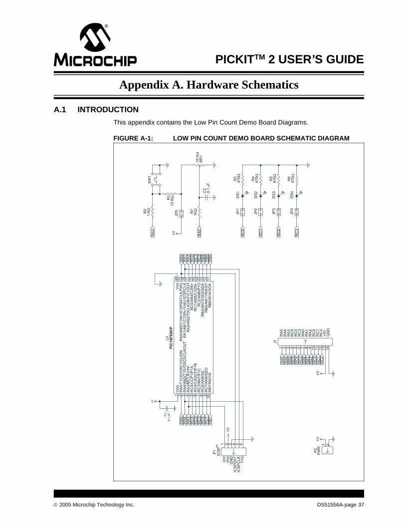
Appendix A. Hardware Schematics
A.1 INTRODUCTION
This appendix contains the Low Pin Count Demo Board Diagrams.
FIGURE A-1: LOW PIN COUNT DEMO BOARD SCHEMATIC DIAGRAM
14
13
12
11
104321 98765
21654321
6 7 8 92 5
13
12
11
10
20
19
18
17
16
15
14
3 41
VP
P
VD
D
GN
D
ICS
PD
AT
ICS
PC
LK
T1G
RC
2/A
N6/P
1D
RC
1/A
N5/C
12IN
-
RC
0/A
N4/C
2IN
+
RA
2/A
N2/T
0C
LK
I/IN
T/C
1O
UT
RA
1/A
N1/C
12IN
-/V
RE
F/IC
SP
CLK
RA
0/A
N0/C
1IN
+/IC
SP
DA
T/U
LP
WU
VS
S
RB
7/R
X/C
K
RC
5/C
CP
1/P
1A
RC
4/C
2O
UT
/P1B
RC
3/A
N7/P
1C
RC
6/A
N8/S
S
RC
7/A
N9/S
DO
VD
D
RB
4/A
N10/S
DI/S
DA
RB
5/A
N11/R
X/D
T
RB
6/S
CK
/SC
K
RA
4/A
N3/T
1G
/OS
C2/C
LK
OU
T
RA
5/T
1C
KI/O
SC
1/C
LK
IN
RA
3/M
CLR
/VP
P
+V
+V
+V
+V
+V
RC
3
RC
2
RC
1
RC
0
RA
3
RA
0
RC
7
RC
6
RB
7R
B6
RB
5
RB
4
RC
2
RC
5
RC
4
RC
3
RC
1
RC
0
RA
5
RA
4
RA
3R
A2
RA
1
RA
0
RC
4
RC
2
RA
5
RA
4
RA
3
RA
2
RA
1
RA
0
RC
5
RC
3
RC
1
RC
0
C1
0.1
μF
C2
0.1
μF
DS
1
DS
2
DS
3
DS
4
J1
JP
1
JP
2
JP
3
JP
4
JP
5
P2
P1
R1
10 K
Ω
R2
1 K
Ω
R3
470
Ω
R4
470
Ω
R5
470
Ω
R6
470
Ω
R7
1K
ΩR
P1
10 K
Ω
SW
1
U1
PIC16F690/P
RA
5
RA
4
RA
3
RC
5
RC
4
RC
3
RA
0
RA
1
RA
2
RC
0
RC
1
RC
2
+5V
GN
D
PW
R
ICS
PT
M
© 2005 Microchip Technology Inc. DS51556A-page 37
DS51556A-page 38 © 2005 Microchip Technology Inc.
AMERICASCorporate Office2355 West Chandler Blvd.Chandler, AZ 85224-6199Tel: 480-792-7200 Fax: 480-792-7277Technical Support: http://support.microchip.comWeb Address: www.microchip.com
AtlantaAlpharetta, GA Tel: 770-640-0034 Fax: 770-640-0307
BostonWestborough, MA Tel: 774-760-0087 Fax: 774-760-0088
ChicagoItasca, IL Tel: 630-285-0071 Fax: 630-285-0075
DallasAddison, TX Tel: 972-818-7423 Fax: 972-818-2924
DetroitFarmington Hills, MI Tel: 248-538-2250Fax: 248-538-2260
KokomoKokomo, IN Tel: 765-864-8360Fax: 765-864-8387
Los AngelesMission Viejo, CA Tel: 949-462-9523 Fax: 949-462-9608
San JoseMountain View, CA Tel: 650-215-1444Fax: 650-961-0286
TorontoMississauga, Ontario, CanadaTel: 905-673-0699 Fax: 905-673-6509
ASIA/PACIFICAustralia - SydneyTel: 61-2-9868-6733 Fax: 61-2-9868-6755
China - BeijingTel: 86-10-8528-2100 Fax: 86-10-8528-2104
China - ChengduTel: 86-28-8676-6200 Fax: 86-28-8676-6599
China - FuzhouTel: 86-591-8750-3506 Fax: 86-591-8750-3521
China - Hong Kong SARTel: 852-2401-1200 Fax: 852-2401-3431
China - ShanghaiTel: 86-21-5407-5533 Fax: 86-21-5407-5066China - ShenyangTel: 86-24-2334-2829Fax: 86-24-2334-2393
China - ShenzhenTel: 86-755-8203-2660 Fax: 86-755-8203-1760
China - ShundeTel: 86-757-2839-5507 Fax: 86-757-2839-5571
China - QingdaoTel: 86-532-502-7355 Fax: 86-532-502-7205
ASIA/PACIFICIndia - BangaloreTel: 91-80-2229-0061 Fax: 91-80-2229-0062
India - New DelhiTel: 91-11-5160-8631Fax: 91-11-5160-8632
Japan - KanagawaTel: 81-45-471- 6166 Fax: 81-45-471-6122
Korea - SeoulTel: 82-2-554-7200 Fax: 82-2-558-5932 or 82-2-558-5934
Malaysia - PenangTel:011-604-646-8870Fax:011-604-646-5086
Philippines - ManilaTel: 011-632-634-9065Fax: 011-632-634-9069
SingaporeTel: 65-6334-8870 Fax: 65-6334-8850
Taiwan - KaohsiungTel: 886-7-536-4818Fax: 886-7-536-4803
Taiwan - TaipeiTel: 886-2-2500-6610 Fax: 886-2-2508-0102
Taiwan - HsinchuTel: 886-3-572-9526Fax: 886-3-572-6459
EUROPEAustria - WeisTel: 43-7242-2244-399Fax: 43-7242-2244-393Denmark - BallerupTel: 45-4450-2828 Fax: 45-4485-2829
France - MassyTel: 33-1-69-53-63-20 Fax: 33-1-69-30-90-79
Germany - IsmaningTel: 49-89-627-144-0 Fax: 49-89-627-144-44
Italy - Milan Tel: 39-0331-742611 Fax: 39-0331-466781
Netherlands - DrunenTel: 31-416-690399 Fax: 31-416-690340
England - BerkshireTel: 44-118-921-5869Fax: 44-118-921-5820
WORLDWIDE SALES AND SERVICE
04/20/05