Embed Size (px)
Citation preview
Low Level Measurements HandbookPrecision DC Current, Voltage, and Resistance Measurements
LowLevelM
easurements
Handbook
6thEdition
www.keithley.com LLM
Keithley Instruments, Inc. Corporate Headquarters • 28775 Aurora Road • Cleveland, Ohio 44139 • 440-248-0400 • Fax: 440-248-6168 • 1-888-KEITHLEY (534-8453) • www.keithley.com
© Copyright 2004 Keithley Instruments, Inc. No. 1559Printed in U.S.A. 80440KSI
Specifications are subject to change without notice.
All Keithley trademarks and trade names are the property of Keithley Instruments, Inc. All other trademarks and trade names are the property of their respective companies.
6thEdition
Low LevelMeasurements
HandbookPrecision DC Current, Voltage,and Resistance Measurements
S I X T H E D I T I O N
A G R E A T E R M E A S U R E O F C O N F I D E N C E

Low Level Measurements Handbook iii
SECTION 1 Low Level DC Measuring Instruments
1.1 Introduction ..................................................................................1-3
1.2 Theoretical Measurement Limits..............................................1-3
1.3 Instrument Definitions................................................................1-51.3.1 The Electrometer..........................................................1-51.3.2 The DMM......................................................................1-71.3.3 The Nanovoltmeter ......................................................1-71.3.4 The Picoammeter..........................................................1-81.3.5 The Source-Measure Unit ............................................1-81.3.6 The SourceMeter® Instrument ....................................1-91.3.7 The Low Current Preamp ............................................1-91.3.8 The Micro-ohmmeter....................................................1-9
1.4 Understanding Instrument Specifications ..........................1-101.4.1 Definition of Accuracy Terms ....................................1-101.4.2 Accuracy ......................................................................1-101.4.3 Deratings ....................................................................1-131.4.4 Noise and Noise Rejection ........................................1-141.4.5 Speed ..........................................................................1-15
1.5 Circuit Design Basics ................................................................1-161.5.1 Voltmeter Circuits ......................................................1-161.5.2 Ammeter Circuits........................................................1-171.5.3 Coulombmeter Circuits ..............................................1-221.5.4 High Resistance Ohmmeter Circuits ..........................1-221.5.5 Low Resistance Ohmmeter Circuits ..........................1-251.5.6 Complete Instruments................................................1-29
SECTION 2 Measurements from High Resistance Sources
2.1 Introduction ..................................................................................2-2
2.2 Voltage Measurements fromHigh Resistance Sources ............................................................2-22.2.1 Loading Errors and Guarding ......................................2-22.2.2 Insulation Resistance..................................................2-11
TA B L E O F CO N T E N T S

iv
2.3 Low Current Measurements....................................................2-142.3.1 Leakage Currents and Guarding ................................2-142.3.2 Noise and Source Impedance ....................................2-192.3.3 Zero Drift ....................................................................2-212.3.4 Generated Currents....................................................2-222.3.5 Voltage Burden ..........................................................2-282.3.6 Overload Protection ..................................................2-302.3.7 AC Interference and Damping ..................................2-312.3.8 Using a Coulombmeter to Measure Low Current......2-33
2.4 High Resistance Measurements ............................................2-362.4.1 Constant-Voltage Method ..........................................2-362.4.2 Constant-Current Method ..........................................2-372.4.3 Characteristics of High Ohmic Valued Resistors ........2-43
2.5 Charge Measurements..............................................................2-442.5.1 Error Sources..............................................................2-442.5.2 Zero Check ................................................................2-452.5.3 Extending the Charge Measurement Range
of the Electrometer ....................................................2-46
2.6 General Electrometer Considerations ..................................2-472.6.1 Making Connections ..................................................2-472.6.2 Electrostatic Interference and Shielding....................2-492.6.3 Environmental Factors................................................2-522.6.4 Speed Considerations ................................................2-532.6.5 Johnson Noise ............................................................2-582.6.6 Device Connections....................................................2-622.6.7 Analog Outputs ..........................................................2-662.6.8 Floating Input Signals ................................................2-672.6.9 Electrometer Verification............................................2-68
SECTION 3 Measurements from Low Resistance Sources
3.1 Introduction ..................................................................................3-2
3.2 Low Voltage Measurements ......................................................3-23.2.1 Offset Voltages ..............................................................3-23.2.2 Noise ..........................................................................3-103.2.3 Common-Mode Current and Reversal Errors ............3-15
Low Level Measurements Handbook v
3.3 Low Resistance Measurements..............................................3-163.3.1 Lead Resistance and Four-Wire Method ....................3-163.3.2 Thermoelectric EMFs and
Offset Compensation Methods ..................................3-193.3.3 Non-Ohmic Contacts ..................................................3-233.3.4 Device Heating ..........................................................3-243.3.5 Dry Circuit Testing......................................................3-253.3.6 Testing Inductive Devices ..........................................3-26
SECTION 4 Applications
4.1 Introduction ..................................................................................4-2
4.2 Applications for Measuring Voltage from High Resistance Sources..................................................4-24.2.1 Capacitor Dielectric Absorption ..................................4-24.2.2 Electrochemical Measurements....................................4-5
4.3 Low Current Measurement Applications ..............................4-94.3.1 Capacitor Leakage Measurements................................4-94.3.2 Low Current Semiconductor Measurements ............4-114.3.3 Light Measurements with Photomultiplier Tubes......4-144.3.4 Ion Beam Measurements............................................4-164.3.5 Avalanche Photodiode Reverse Bias Current
Measurements ............................................................4-18
4.4 High Resistance Measurement Applications ......................4-204.4.1 Surface Insulation Resistance Testing
of Printed Circuit Boards............................................4-204.4.2 Resistivity Measurements of Insulating Materials ......4-224.4.3 Resistivity Measurements of Semiconductors ............4-264.4.4 Voltage Coefficient Testing of
High Ohmic Value Resistors ......................................4-35
4.5 Charge Measurement Applications ......................................4-364.5.1 Capacitance Measurements ........................................4-374.5.2 Using a Faraday Cup to Measure
Static Charge on Objects ............................................4-38
4.6 Low Voltage Measurement Applications ............................4-394.6.1 Standard Cell Comparisons........................................4-39

vi
4.6.2 High Resolution Temperature Measurements and Microcalorimetry ................................................4-42
4.7 Low Resistance Measurement Applications ......................4-444.7.1 Contact Resistance......................................................4-444.7.2 Superconductor Resistance Measurements ..............4-474.7.3 Resistivity Measurements of Conductive Materials ....4-50
SECTION 5 Low Level Instrument Selection Guide
5.1 Introduction ..................................................................................5-2
5.2 Instrument and Accessory Selector Guides ..........................5-2
APPENDIX A Low Level Measurement Troubleshooting Guide
APPENDIX B Cable and Connector Assembly
APPENDIX C Glossary
APPENDIX D Safety Considerations
INDEX
S E C T I O N 1
Low Level DCMeasuring
Instruments
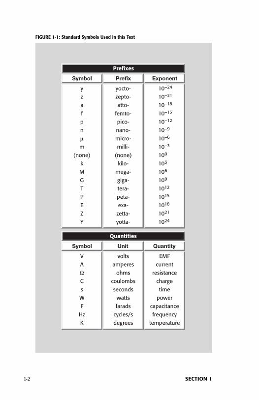
FIGURE 1-1: Standard Symbols Used in this Text
1-2 SECTION 1
UnitSymbol Quantity
Quantities
VAΩCsWF
HzK
EMFcurrent
resistancechargetime
powercapacitancefrequency
temperature
voltsamperes
ohmscoulombsseconds
wattsfarads
cycles/sdegrees
PrefixSymbol Exponent
Prefixes
yzafpnµm
(none)kMGTPEZY
yocto-zepto-atto-
femto-pico-nano-micro-milli-
(none)kilo-
mega-giga-tera-peta-exa-
zetta-yotta-
10–24
10–21
10–18
10–15
10–12
10–9
10–6
10–3
100
103
106
109
1012
1015
1018
1021
1024
1.1 IntroductionDC voltage, DC current, and resistance are measured most often with digi-tal multimeters (DMMs). Generally, these instruments are adequate formeasurements at signal levels greater than 1µV or 1µA, or less than 1GΩ.(See Figure 1-1 for standard symbols used in this text.) However, they don’tapproach the theoretical limits of sensitivity. For low level signals, more sen-sitive instruments such as electrometers, picoammeters, and nanovolt-meters must be used.
Section 1 offers an overview of the theoretical limits of DC measure-ments and the instruments used to make them. It includes instrumentdescriptions and basic instrument circuit designs. For easier reference, thisinformation is organized into a number of subsections:
1.2 Theoretical Measurement Limits: A discussion of both the theoreticalmeasurement limitations and instrument limitations for low level meas-urements.
1.3 Instrument Definitions: Descriptions of electrometers, DMMs, nano-voltmeters, picoammeters, source-measure units, SourceMeter® instru-ments, low current preamps, and micro-ohmmeters.
1.4 Understanding Instrument Specifications: A review of the terminologyused in instrument specifications, such as accuracy (resolution, sensi-tivity, transfer stability), deratings (temperature coefficient, time drift),noise (NMRR and CMRR), and speed.
1.5 Circuit Design Basics: Describes basic circuit design for voltmeter cir-cuits (electrometer, nanovoltmeter) and ammeter circuits (shunt amme-ter, feedback picoammeter, high speed picoammeter, logarithmicpicoammeter).
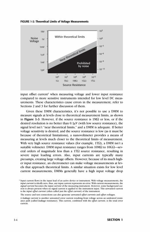
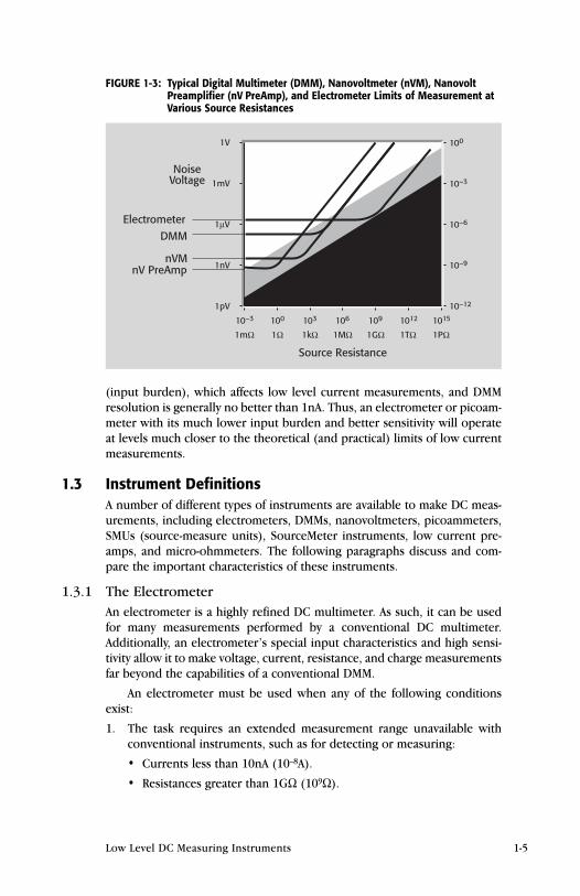
1.2 Theoretical Measurement LimitsThe theoretical limit of sensitivity in any measurement is determined by thenoise generated by the resistances present in the circuit. As discussed inSections 2.6.5 and 3.2.2, voltage noise is proportional to the square root ofthe resistance, bandwidth, and absolute temperature. Figure 1-2 shows the-oretical voltage measurement limits at room temperature (300K) with aresponse time of 0.1 second to ten seconds. Note that high source resist-ance limits the theoretical sensitivity of the voltage measurement. While it’scertainly possible to measure a 1µV signal that has a 1Ω source resistance,it’s not possible to measure that same 1µV signal level from a 1TΩ source.Even with a much lower 1MΩ source resistance, a 1µV measurement is neartheoretical limits, so it would be very difficult to make using an ordinaryDMM.
In addition to having insufficient voltage or current sensitivity (mostDMMs are no more sensitive than 1µV or 1nA per digit), DMMs have high
Low Level DC Measuring Instruments 1-3
input offset current1 when measuring voltage and lower input resistancecompared to more sensitive instruments intended for low level DC meas-urements. These characteristics cause errors in the measurement; refer toSections 2 and 3 for further discussion of them.
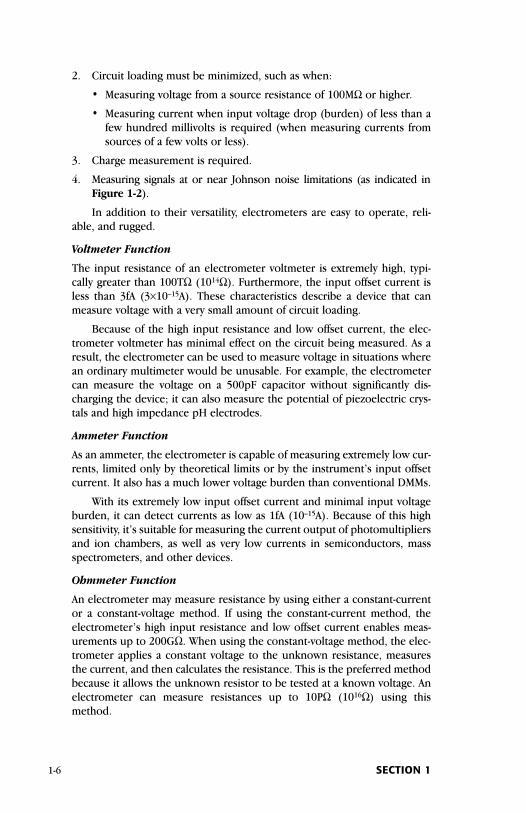
Given these DMM characteristics, it’s not possible to use a DMM tomeasure signals at levels close to theoretical measurement limits, as shownin Figure 1-3. However, if the source resistance is 1MΩ or less, or if thedesired resolution is no better than 0.1µV (with low source resistance), thesignal level isn’t “near theoretical limits,” and a DMM is adequate. If bettervoltage sensitivity is desired, and the source resistance is low (as it must bebecause of theoretical limitations), a nanovoltmeter provides a means ofmeasuring at levels much closer to the theoretical limits of measurement.With very high source resistance values (for example, 1TΩ), a DMM isn’t asuitable voltmeter. DMM input resistance ranges from 10MΩ to 10GΩ—sev-eral orders of magnitude less than a 1TΩ source resistance, resulting insevere input loading errors. Also, input currents are typically manypicoamps, creating large voltage offsets. However, because of its much high-er input resistance, an electrometer can make voltage measurements at lev-els that approach theoretical limits. A similar situation exists for low levelcurrent measurements; DMMs generally have a high input voltage drop
1-4 SECTION 1
FIGURE 1-2: Theoretical Limits of Voltage Measurements
103
100
10–3
10–6
10–9
10–12
1kV
1V
1mV
1µV
1nV
1pV
100 103 106 109 1012
1Ω 1kΩ 1MΩ 1GΩ 1TΩ
Within theoretical limits
Near theoretical limits
Prohibitedby noise
NoiseVoltage
Source Resistance
1 Input current flows in the input lead of an active device or instrument. With voltage measurements, theinput current is ideally zero; thus, any input current represents an error. With current measurements, thesignal current becomes the input current of the measuring instrument. However, some background cur-rent is always present when no signal current is applied to the instrument input. This unwanted currentis the input offset current (often called just the offset current) of the instrument.The source and test connections can also generate unwanted offset currents and offset voltages.A leakage current is another unwanted error current resulting from voltage across an undesired resist-ance path (called leakage resistance). This current, combined with the offset current, is the total errorcurrent.
(input burden), which affects low level current measurements, and DMMresolution is generally no better than 1nA. Thus, an electrometer or picoam-meter with its much lower input burden and better sensitivity will operateat levels much closer to the theoretical (and practical) limits of low currentmeasurements.
1.3 Instrument DefinitionsA number of different types of instruments are available to make DC meas-urements, including electrometers, DMMs, nanovoltmeters, picoammeters,SMUs (source-measure units), SourceMeter instruments, low current pre-amps, and micro-ohmmeters. The following paragraphs discuss and com-pare the important characteristics of these instruments.
1.3.1 The ElectrometerAn electrometer is a highly refined DC multimeter. As such, it can be usedfor many measurements performed by a conventional DC multimeter.Additionally, an electrometer’s special input characteristics and high sensi-tivity allow it to make voltage, current, resistance, and charge measurementsfar beyond the capabilities of a conventional DMM.
An electrometer must be used when any of the following conditionsexist:
1. The task requires an extended measurement range unavailable withconventional instruments, such as for detecting or measuring:
• Currents less than 10nA (10–8A).
• Resistances greater than 1GΩ (109Ω).
Low Level DC Measuring Instruments 1-5
100
10–3
10–6
10–9
10–12
1V
1mV
1µV
1nV
1pV
100 103 106 109 1012
1Ω 1kΩ 1MΩ 1GΩ 1TΩ
NoiseVoltage
Source Resistance
1015
1PΩ
DMM
Electrometer
nV PreAmpnVM
10–3
1mΩ
FIGURE 1-3: Typical Digital Multimeter (DMM), Nanovoltmeter (nVM), NanovoltPreamplifier (nV PreAmp), and Electrometer Limits of Measurement atVarious Source Resistances
2. Circuit loading must be minimized, such as when:
• Measuring voltage from a source resistance of 100MΩ or higher.
• Measuring current when input voltage drop (burden) of less than afew hundred millivolts is required (when measuring currents fromsources of a few volts or less).
3. Charge measurement is required.
4. Measuring signals at or near Johnson noise limitations (as indicated inFigure 1-2).
In addition to their versatility, electrometers are easy to operate, reli-able, and rugged.
Voltmeter Function
The input resistance of an electrometer voltmeter is extremely high, typi-cally greater than 100TΩ (1014Ω). Furthermore, the input offset current isless than 3fA (3×10–15A). These characteristics describe a device that canmeasure voltage with a very small amount of circuit loading.
Because of the high input resistance and low offset current, the elec-trometer voltmeter has minimal effect on the circuit being measured. As aresult, the electrometer can be used to measure voltage in situations wherean ordinary multimeter would be unusable. For example, the electrometercan measure the voltage on a 500pF capacitor without significantly dis-charging the device; it can also measure the potential of piezoelectric crys-tals and high impedance pH electrodes.
Ammeter Function
As an ammeter, the electrometer is capable of measuring extremely low cur-rents, limited only by theoretical limits or by the instrument’s input offsetcurrent. It also has a much lower voltage burden than conventional DMMs.
With its extremely low input offset current and minimal input voltageburden, it can detect currents as low as 1fA (10–15A). Because of this highsensitivity, it’s suitable for measuring the current output of photomultipliersand ion chambers, as well as very low currents in semiconductors, massspectrometers, and other devices.
Ohmmeter Function
An electrometer may measure resistance by using either a constant-currentor a constant-voltage method. If using the constant-current method, theelectrometer’s high input resistance and low offset current enables meas-urements up to 200GΩ. When using the constant-voltage method, the elec-trometer applies a constant voltage to the unknown resistance, measuresthe current, and then calculates the resistance. This is the preferred methodbecause it allows the unknown resistor to be tested at a known voltage. Anelectrometer can measure resistances up to 10PΩ (1016Ω) using thismethod.
1-6 SECTION 1
Coulombmeter Function
Current integration and measurement of charge are electrometer coulomb-meter capabilities not found in multimeters. The electrometer coulombme-ter can detect charge as low as 10fC (10–14C). It’s equivalent to an activeintegrator and, therefore, has low voltage burden, typically less than 100µV.
The coulombmeter function can measure lower currents than theammeter function can, because no noise is contributed by internal resistors.Currents as low as 1fA (10–15A) may be detected using this function. SeeSection 2.3.8 for further details.
1.3.2 The DMMDigital multimeters vary widely in performance, from low cost handheld 31⁄2-digit units to high precision system DMMs. While there are many modelsavailable from a wide variety of manufacturers, none approaches the theo-retical limits of measurement discussed previously. These limitations don’timply that DMMs are inadequate instruments; they simply point out the factthat the vast majority of measurements are made at levels far from theoret-ical limits, and DMMs are designed to meet these more conventional meas-urement needs.
Although low level measurements are by definition those that are closeto theoretical limits, and are thus outside the range of DMMs, advances intechnology are narrowing the gap between DMMs and dedicated low levelinstruments. For example, the most sensitive DMMs can detect DC voltagesas low as 10nV, resolve DC currents down to 10pA, and measure resistancesas high as 1GΩ. While these characteristics still fall far short of the corre-sponding capabilities of more sensitive instruments like the electrometerdescribed previously, all the measurement theory and accuracy considera-tions in this book apply to DMM measurements as well as to nanovoltmeter,picoammeter, electrometer, or SMU measurements. The difference is only amatter of degree; when making measurements close to theoretical limits, allmeasurement considerations are vitally important. When measuring at lev-els far from theoretical limits, only a few basic considerations (accuracy,loading, etc.) are generally of concern.
1.3.3 The NanovoltmeterA nanovoltmeter is a very sensitive voltage meter. As shown in Figure 1-3,this type of instrument is optimized to provide voltage measurements nearthe theoretical limits from low source resistances, in contrast to the elec-trometer, which is optimized for use with high source resistances.Compared to an electrometer, the voltage noise and drift are much lower,and the current noise and drift are much higher. Input resistance is usuallysimilar to that of a DMM and is much lower than that of an electrometer.
As is the case with electrometers, nanovoltmeters are just as reliable andeasy to operate as DMMs. Their distinguishing characteristic is their voltagesensitivity, which can be as good as 1pV. Most nanovoltmeters aren’t multi-
Low Level DC Measuring Instruments 1-7
function instruments and are correspondingly less complex thanelectrometers.
1.3.4 The Picoammeter
A picoammeter is an ammeter built along the lines of the ammeter functionof an electrometer. When compared with an electrometer, a picoammeterhas a similar low voltage burden, similar or faster speed, less sensitivity, anda lower price. It may also have special characteristics, such as high speedlogarithmic response or a built-in voltage source.
1.3.5 The Source-Measure Unit
As its name implies, a source-measure unit (SMU) has both measuring andsourcing capabilities. Adding current and voltage sourcing capabilities to ameasuring instrument provides an extra degree of versatility for many lowlevel measurement applications. For example, very high resistance valuescan be determined by applying a voltage across a device and measuring theresulting current. The added sourcing functions also make a SMU more con-venient and versatile than using separate instruments for such applicationsas generating I-V curves of semiconductors and other types of devices.
The typical SMU provides the following four functions:
• Measure voltage
• Measure current
• Source voltage
• Source current
These functions can be used separately or they can be used together inthe following combinations:
• Simultaneously source voltage and measure current, or
• Simultaneously source current and measure voltage.
SMUs have a number of electrometer-like characteristics that makethem suitable for low level measurements. The input resistance is very high(typically 100TΩ or more), minimizing circuit loading when making voltagemeasurements from high impedance sources. The current measurementsensitivity is also similar to that of the electrometer picoammeter—typicallyas low as 10fA.
Another important advantage of many source-measure units is theirsweep capability. Either voltage or current can be swept across the desiredrange at specified increments, and the resulting current or voltage can bemeasured at each step. Built-in source-delay-measure cycles allow optimiz-ing measurement speed while ensuring sufficient circuit settling time tomaintain measurement integrity.
1-8 SECTION 1

1.3.6 The SourceMeter® Instrument
The SourceMeter instrument is very similar to the source-measure unit inmany ways, including its ability to source and measure both current andvoltage and to perform sweeps. In addition, a SourceMeter instrument candisplay the measurements directly in resistance, as well as voltage andcurrent.
The typical SourceMeter instrument doesn’t have as high an inputimpedance or as low a current capability as a source-measure unit. TheSourceMeter instrument is designed for general-purpose, high speed pro-duction test applications. It can be used as a source for moderate to lowlevel measurements and for research applications.
Unlike a DMM, which can make a measurement at only one point, aSourceMeter instrument can be used to generate a family of curves, becauseit has a built-in source. This is especially useful when studying semiconduc-tor devices and making materials measurements.
When used as a current source, a SourceMeter instrument can be usedin conjunction with a nanovoltmeter to measure very low resistances byautomatically reversing the polarity of the source to correct for offsets.
1.3.7 The Low Current Preamp
Some SMUs and SourceMeter instruments may have a remote low currentpreamp. With this design, the sensitive amplifier circuitry is separate fromthe SMU or SourceMeter instrument. This makes it possible to place themost sensitive part of the instrument very close to the device being tested,thereby eliminating a major source of error, the noise and leakage from thecables themselves.
1.3.8 The Micro-ohmmeter
A micro-ohmmeter is a special type of ohmmeter designed especially formaking low level resistance measurements. While the techniques used formaking resistance measurements are similar to those used in a DMM, micro-ohmmeter circuits are optimized for making low level measurements. Thetypical micro-ohmmeter can resolve resistances as low as 10µΩ.
Measurements made using the micro-ohmmeter are always performedusing the four-wire technique in order to minimize errors caused by testleads and connections. The typical micro-ohmmeter also has additional fea-tures such as offset compensation and dry circuit testing to optimize lowresistance measurements. Offset compensation is performed by pulsing thetest current to cancel offsets from thermoelectric EMFs. The dry circuit testmode limits the voltage across the unknown resistance to a very small value(typically <20mV) to avoid puncturing oxides when testing such devices asrelay contacts, connectors, and switches.
Low Level DC Measuring Instruments 1-9
1.4 Understanding Instrument SpecificationsKnowing how to interpret instrument specifications properly is an impor-tant aspect of making good low level measurements. Although instrumentaccuracy is probably the most important of these specifications, there areseveral other factors to consider when reviewing specifications, includingnoise, deratings, and speed.
1.4.1 Definition of Accuracy TermsThis section defines a number of terms related to instrument accuracy.Some of these terms are further discussed in subsequent paragraphs. Table1-1 summarizes conversion factors for various specifications associated withinstruments.
SENSITIVITY - the smallest change in the signal that can be detected.
RESOLUTION - the smallest portion of the signal that can be observed.
REPEATABILITY - the closeness of agreement between successive measure-ments carried out under the same conditions.
REPRODUCIBILITY - the closeness of agreement between measurements ofthe same quantity carried out with a stated change in conditions.
ABSOLUTE ACCURACY - the closeness of agreement between the result of ameasurement and its true value or accepted standard value. Accuracyis often separated into gain and offset terms.
RELATIVE ACCURACY - the extent to which a measurement accuratelyreflects the relationship between an unknown and a reference value.
ERROR - the deviation (difference or ratio) of a measurement from its truevalue. Note that true values are by their nature indeterminate.
RANDOM ERROR - the mean of a large number of measurements influencedby random error matches the true value.
SYSTEMATIC ERROR - the mean of a large number of measurements influ-enced by systematic error deviates from the true value.
UNCERTAINTY - an estimate of the possible error in a measurement, i.e., theestimated possible deviation from its actual value. This is the oppositeof accuracy.
“Precision” is a more qualitative term than many of those defined here.It refers to the freedom from uncertainty in the measurement. It’s oftenapplied in the context of repeatability or reproducibility, but it shouldn’t beused in place of “accuracy.”
1.4.2 AccuracyOne of the most important considerations in any measurement situation isreading accuracy. For any given test setup, a number of factors can affectaccuracy. The most important factor is the accuracy of the instrument itself,which may be specified in several ways, including a percentage of full scale,
1-10 SECTION 1
a percentage of reading, or a combination of both. Instrument accuracyaspects are covered in the following paragraphs.
Other factors such as input loading, leakage resistance and current,shielding, and guarding may also have a serious impact on overall accuracy.These important measurement considerations are discussed in detail inSections 2 and 3.
Measurement Instrument Specifications
Instrument accuracy is usually specified as a percent of reading, plus a per-centage of range (or a number of counts of the least significant digit). Forexample, a typical DMM accuracy specification may be stated as: ±(0.005%of reading + 0.002% of range). Note that the percent of reading is most sig-nificant when the reading is close to full scale, while the percent of range ismost significant when the reading is a small fraction of full scale.
Accuracy may also be specified in ppm (parts per million). Typically, thisaccuracy specification is given as ±(ppm of reading + ppm of range). Forexample, the DCV accuracy of a higher resolution DMM might be specifiedas ±(25ppm of reading + 5ppm of range).
Resolution
The resolution of a digital instrument is determined by the number ofcounts that can be displayed, which depends on the number of digits. A typ-ical digital electrometer might have 51⁄2 digits, meaning five whole digits(each with possible values between 0 and 9) plus a leading half digit thatcan take on the values 0 or ±1. Thus, a 51⁄2-digit display can show 0 to199,999, a total of 200,000 counts. The resolution of the display is the ratioof the smallest count to the maximum count (1/200,000 or 0.0005% for a51⁄2-digit display).
Low Level DC Measuring Instruments 1-11
Percent PPM Digits Bits dBPortionof 10V
Number of timeconstants to settleto rated accuracy
10% 100000 1 3.3 –20 1 V 2.3
1% 10000 2 6.6 –40 100mV 4.6
0.1% 1000 3 10 –60 10mV 6.9
0.01% 100 4 13.3 –80 1mV 9.2
0.001% 10 5 16.6 –100 100 µV 11.5
0.0001% 1 6 19.9 –120 10 µV 13.8
0.00001% 0.1 7 23.3 –140 1 µV 16.1
0.000001% 0.01 8 26.6 –160 100 nV 18.4
0.000001% 0.001 9 29.9 –180 10 nV 20.7
TABLE 1-1: Specification Conversion Factors
For example, the specification of ±(0.05% + 1 count) on a 41⁄2-digitmeter reading 10.000 volts corresponds to a total error of ±(5mV + 1mV)out of 10V, or ±(0.05% of reading + 0.01% of reading), totaling ±0.06%.Generally, the higher the resolution, the better the accuracy.
Sensitivity
The sensitivity of a measurement is the smallest change of the measured sig-nal that can be detected. For example, voltage sensitivity may be 1µV, whichsimply means that any change in input signal less than 1µV won’t show upin the reading. Similarly, a current sensitivity of 10fA implies that onlychanges in current greater than that value will be detected.
The ultimate sensitivity of a measuring instrument depends on both itsresolution and the lowest measurement range. For example, the sensitivityof a 51⁄2-digit DMM with a 200mV measurement range is 1µV.
Absolute and Relative Accuracy
As shown in Figure 1-4, absolute accuracy is the measure of instrumentaccuracy that is directly traceable to the primary standard at the NationalInstitute of Standards and Technology (NIST). Absolute accuracy may bespecified as ±(% of reading + counts), or it can be stated as ±(ppm of read-ing + ppm of range), where ppm signifies parts per million of error.
FIGURE 1-4: Comparison of Absolute and Relative Accuracy
Relative accuracy (see Figure 1-4) specifies instrument accuracy tosome secondary reference standard. As with absolute accuracy, relative accu-racy can be specified as ±(% of reading + counts) or it may be stated as±(ppm of reading + ppm of range).
NISTStandard
SecondaryStandard
MeasuringInstrument
DeviceUnder Test
RelativeAccuracy
AbsoluteAccuracy
1-12 SECTION 1
Transfer Stability
A special case of relative accuracy is the transfer stability, which definesinstrument accuracy relative to a secondary reference standard over a veryshort time span and narrow ambient temperature range (typically withinfive minutes and ±1°C). The transfer stability specification is useful in situ-ations where highly accurate measurements must be made in reference to aknown secondary standard.
Calculating Error Terms from Accuracy Specifications
To illustrate how to calculate measurement errors from instrument specifi-cations, assume the following measurement parameters:
Accuracy: ±(25ppm of reading + 5ppm of range)Range: 2VInput signal: 1.5V
The error is calculated as:
Error = 1.5(25 × 10–6) + 2(5 × 10⁻⁶)= (37.5 × 10⁻⁶) + (10 × 10–6)= 47.5 × 10⁻⁶
Thus, the reading could fall anywhere within the range of 1.5V ±47.5µV, an error of ±0.003%.
1.4.3 DeratingsAccuracy specifications are subject to deratings for temperature and timedrift, as discussed in the following paragraphs.
Temperature Coefficient
The temperature of the operating environment can affect accuracy. For thisreason, instrument specifications are usually given over a defined tempera-ture range. Keithley accuracy specifications on newer electrometers, nano-voltmeters, DMMs, and SMUs are usually given over the range of 18°C to28°C. For temperatures outside of this range, a temperature coefficient suchas ±(0.005 % + 0.1 count)/°C or ±(5ppm of reading + 1ppm of range)/°Cis specified. As with the accuracy specification, this value is given as a per-centage of reading plus a number of counts of the least significant digit (oras a ppm of reading plus ppm of range) for digital instruments. If the instru-ment is operated outside the 18°C to 28°C temperature range, this figuremust be taken into account, and errors can be calculated in the mannerdescribed previously for every degree less than 18°C or greater than 28°C.
Time Drift
Most electronic instruments, including electrometers, picoammeters, nano-voltmeters, DMMs, SMUs, and SourceMeter instruments, are subject tochanges in accuracy and other parameters over a long period of time,whether or not the equipment is operating. Because of these changes,instrument specifications usually include a time period beyond which the
Low Level DC Measuring Instruments 1-13
instrument’s accuracy cannot be guaranteed. The time period is stated inthe specifications, and is typically over specific increments such as 90 daysor one year. As noted previously, transfer stability specifications are definedfor a much shorter period of time—typically five or 10 minutes.
1.4.4 Noise and Noise Rejection
Noise is often a consideration when making virtually any type of electronicmeasurement, but noise problems can be particularly severe when makinglow level measurements. Thus, it’s important that noise specifications andterms are well understood when evaluating the performance of an instru-ment.
Normal Mode Rejection Ratio
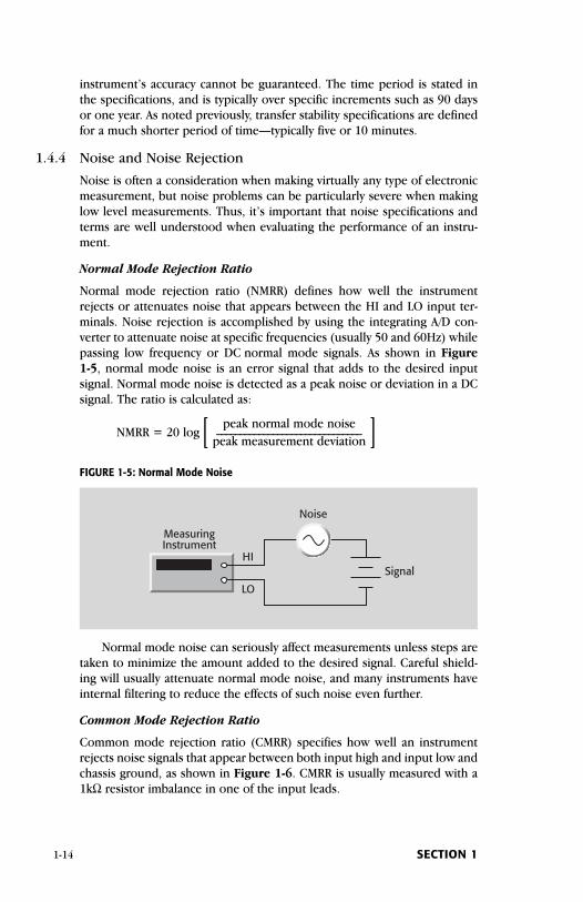
Normal mode rejection ratio (NMRR) defines how well the instrumentrejects or attenuates noise that appears between the HI and LO input ter-minals. Noise rejection is accomplished by using the integrating A/D con-verter to attenuate noise at specific frequencies (usually 50 and 60Hz) whilepassing low frequency or DC normal mode signals. As shown in Figure 1-5, normal mode noise is an error signal that adds to the desired inputsignal. Normal mode noise is detected as a peak noise or deviation in a DCsignal. The ratio is calculated as:
peak normal mode noiseNMRR = 20 log _______________________________[ peak measurement deviation ]
FIGURE 1-5: Normal Mode Noise
Normal mode noise can seriously affect measurements unless steps aretaken to minimize the amount added to the desired signal. Careful shield-ing will usually attenuate normal mode noise, and many instruments haveinternal filtering to reduce the effects of such noise even further.
Common Mode Rejection Ratio
Common mode rejection ratio (CMRR) specifies how well an instrumentrejects noise signals that appear between both input high and input low andchassis ground, as shown in Figure 1-6. CMRR is usually measured with a1kΩ resistor imbalance in one of the input leads.
MeasuringInstrument
HI
LO
Noise
Signal
1-14 SECTION 1
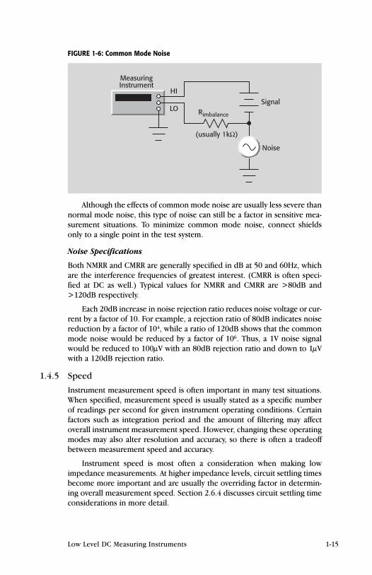
FIGURE 1-6: Common Mode Noise
Although the effects of common mode noise are usually less severe thannormal mode noise, this type of noise can still be a factor in sensitive mea-surement situations. To minimize common mode noise, connect shieldsonly to a single point in the test system.
Noise Specifications
Both NMRR and CMRR are generally specified in dB at 50 and 60Hz, whichare the interference frequencies of greatest interest. (CMRR is often speci-fied at DC as well.) Typical values for NMRR and CMRR are >80dB and>120dB respectively.
Each 20dB increase in noise rejection ratio reduces noise voltage or cur-rent by a factor of 10. For example, a rejection ratio of 80dB indicates noisereduction by a factor of 104, while a ratio of 120dB shows that the commonmode noise would be reduced by a factor of 106. Thus, a 1V noise signalwould be reduced to 100µV with an 80dB rejection ratio and down to 1µVwith a 120dB rejection ratio.
1.4.5 Speed
Instrument measurement speed is often important in many test situations.When specified, measurement speed is usually stated as a specific numberof readings per second for given instrument operating conditions. Certainfactors such as integration period and the amount of filtering may affectoverall instrument measurement speed. However, changing these operatingmodes may also alter resolution and accuracy, so there is often a tradeoffbetween measurement speed and accuracy.
Instrument speed is most often a consideration when making lowimpedance measurements. At higher impedance levels, circuit settling timesbecome more important and are usually the overriding factor in determin-ing overall measurement speed. Section 2.6.4 discusses circuit settling timeconsiderations in more detail.
MeasuringInstrument
HI
LO
Noise
SignalRimbalance
(usually 1kΩ)
Low Level DC Measuring Instruments 1-15
1.5 Circuit Design Basics
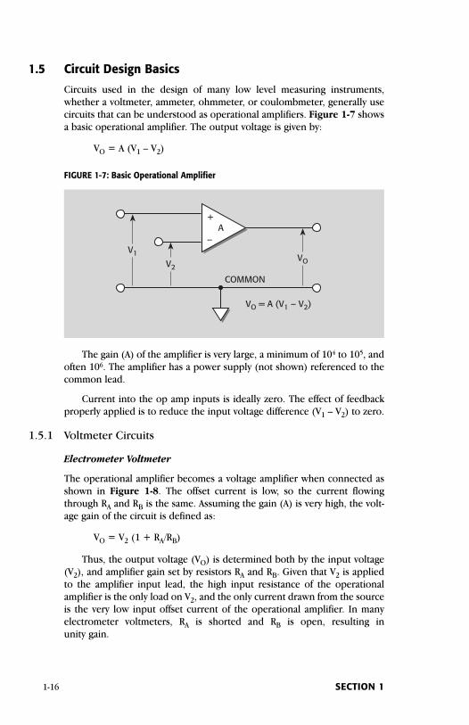
Circuits used in the design of many low level measuring instruments,whether a voltmeter, ammeter, ohmmeter, or coulombmeter, generally usecircuits that can be understood as operational amplifiers. Figure 1-7 showsa basic operational amplifier. The output voltage is given by:
VO = A (V1 – V2)
FIGURE 1-7: Basic Operational Amplifier
The gain (A) of the amplifier is very large, a minimum of 104 to 105, andoften 106. The amplifier has a power supply (not shown) referenced to thecommon lead.
Current into the op amp inputs is ideally zero. The effect of feedbackproperly applied is to reduce the input voltage difference (V1 – V2) to zero.
1.5.1 Voltmeter Circuits
Electrometer Voltmeter
The operational amplifier becomes a voltage amplifier when connected asshown in Figure 1-8. The offset current is low, so the current flowingthrough RA and RB is the same. Assuming the gain (A) is very high, the volt-age gain of the circuit is defined as:
VO = V2 (1 + RA/RB)
Thus, the output voltage (VO) is determined both by the input voltage(V2), and amplifier gain set by resistors RA and RB. Given that V2 is appliedto the amplifier input lead, the high input resistance of the operationalamplifier is the only load on V2, and the only current drawn from the sourceis the very low input offset current of the operational amplifier. In manyelectrometer voltmeters, RA is shorted and RB is open, resulting in unity gain.
V2
+
–V1 VO
A
VO = A (V1 – V2)
COMMON
1-16 SECTION 1

Low Level DC Measuring Instruments 1-17
Nanovoltmeter Preamplifier
The same basic circuit configuration shown in Figure 1-8 can be used as aninput preamplifier for a nanovoltmeter. Much higher voltage gain isrequired, so the values of RA and RB are set accordingly; a typical voltagegain for a nanovoltmeter preamplifier is 103.
Electrometer and nanovoltmeter characteristics differ, so the opera-tional amplifier requirements for these two types of instruments are alsosomewhat different. While the most important characteristics of the elec-trometer voltmeter operational amplifier are low input offset current andhigh input impedance, the most important requirement for the nanovolt-meter input preamplifier is low input noise voltage.
1.5.2 Ammeter CircuitsThere are two basic techniques for making current measurements: these arethe shunt ammeter and the feedback ammeter techniques. DMMs and olderelectrometers use the shunt method, while picoammeters and the AMPSfunction of electrometers use the feedback ammeter configuration only.
Shunt Ammeter
Shunting the input of a voltmeter with a resistor forms a shunt ammeter, asshown in Figure 1-9. The input current (IIN) flows through the shunt resis-tor (RS). The output voltage is defined as:
VO = IIN RS (1 + RA/RB)
For several reasons, it’s generally advantageous to use the smallest pos-sible value for RS.
First, low value resistors have better accuracy, time and temperature sta-bility, and voltage coefficient than high value resistors. Second, lower resistor
V2
+
–
V1
VO
A
RA
RB
VO = V2 (1 + RA/RB)
FIGURE 1-8: Voltage Amplifier
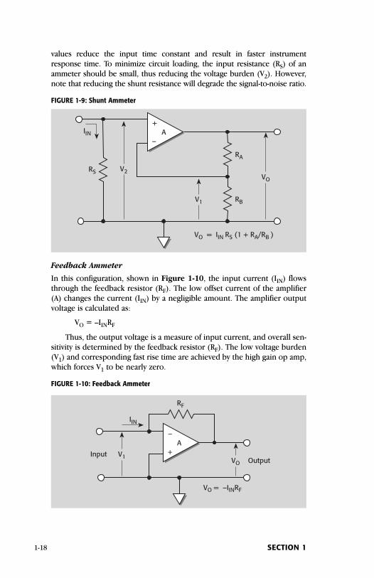
values reduce the input time constant and result in faster instrumentresponse time. To minimize circuit loading, the input resistance (RS) of anammeter should be small, thus reducing the voltage burden (V2). However,note that reducing the shunt resistance will degrade the signal-to-noise ratio.
FIGURE 1-9: Shunt Ammeter
Feedback Ammeter
In this configuration, shown in Figure 1-10, the input current (IIN) flowsthrough the feedback resistor (RF). The low offset current of the amplifier(A) changes the current (IIN) by a negligible amount. The amplifier outputvoltage is calculated as:
VO = –IINRF
Thus, the output voltage is a measure of input current, and overall sen-sitivity is determined by the feedback resistor (RF). The low voltage burden(V1) and corresponding fast rise time are achieved by the high gain op amp,which forces V1 to be nearly zero.
FIGURE 1-10: Feedback Ammeter
V1
–
+VO
A
IIN
RF
InputOutput
VO = –IINRF
V2
+
–
V1
VO
A
RA
RB
RS
IIN
VO = IIN RS (1 + RA/RB )
1-18 SECTION 1
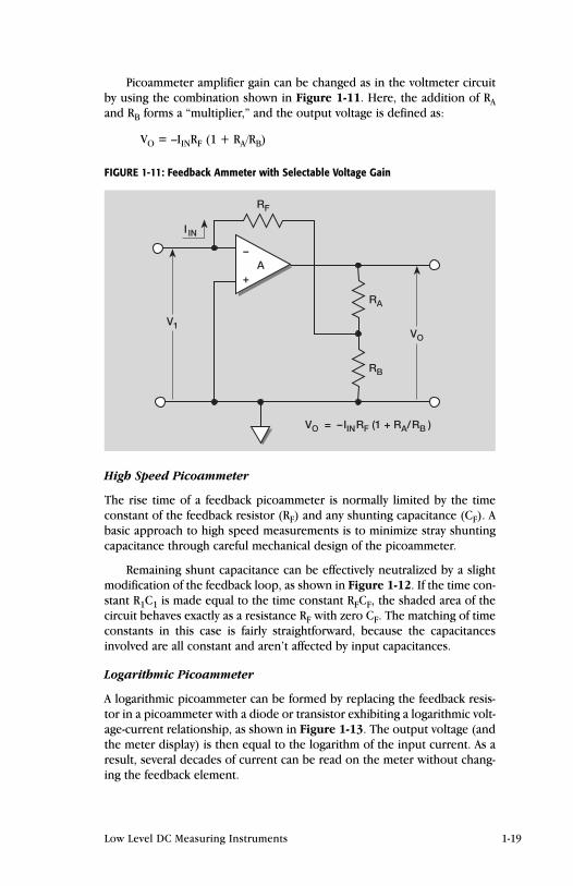
Picoammeter amplifier gain can be changed as in the voltmeter circuitby using the combination shown in Figure 1-11. Here, the addition of RAand RB forms a “multiplier,” and the output voltage is defined as:
VO = –IINRF (1 + RA/RB)
FIGURE 1-11: Feedback Ammeter with Selectable Voltage Gain
High Speed Picoammeter
The rise time of a feedback picoammeter is normally limited by the timeconstant of the feedback resistor (RF) and any shunting capacitance (CF). Abasic approach to high speed measurements is to minimize stray shuntingcapacitance through careful mechanical design of the picoammeter.
Remaining shunt capacitance can be effectively neutralized by a slightmodification of the feedback loop, as shown in Figure 1-12. If the time con-stant R1C1 is made equal to the time constant RFCF, the shaded area of thecircuit behaves exactly as a resistance RF with zero CF. The matching of timeconstants in this case is fairly straightforward, because the capacitancesinvolved are all constant and aren’t affected by input capacitances.
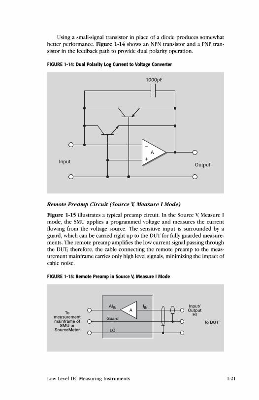
Logarithmic Picoammeter
A logarithmic picoammeter can be formed by replacing the feedback resis-tor in a picoammeter with a diode or transistor exhibiting a logarithmic volt-age-current relationship, as shown in Figure 1-13. The output voltage (andthe meter display) is then equal to the logarithm of the input current. As aresult, several decades of current can be read on the meter without chang-ing the feedback element.
V1
–
+
VO
A
RA
RB
I IN
RF
VO = –IINRF (1 + RA/RB )
Low Level DC Measuring Instruments 1-19
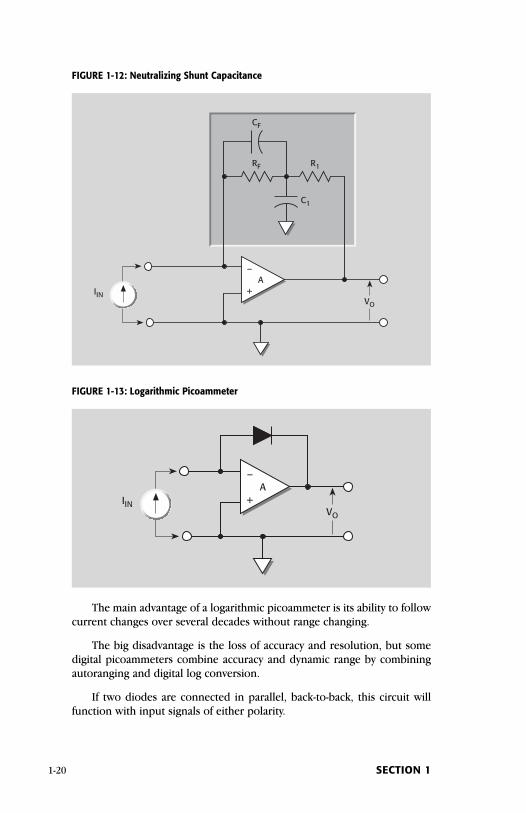
FIGURE 1-12: Neutralizing Shunt Capacitance
FIGURE 1-13: Logarithmic Picoammeter
The main advantage of a logarithmic picoammeter is its ability to followcurrent changes over several decades without range changing.
The big disadvantage is the loss of accuracy and resolution, but somedigital picoammeters combine accuracy and dynamic range by combiningautoranging and digital log conversion.
If two diodes are connected in parallel, back-to-back, this circuit willfunction with input signals of either polarity.
–
+VO
AIIN
–
+VO
A
RF
IIN
CF
C1
R1
1-20 SECTION 1
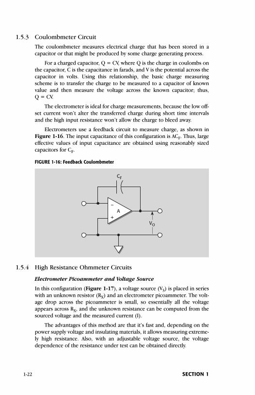
Using a small-signal transistor in place of a diode produces somewhatbetter performance. Figure 1-14 shows an NPN transistor and a PNP tran-sistor in the feedback path to provide dual polarity operation.
FIGURE 1-14: Dual Polarity Log Current to Voltage Converter
Remote Preamp Circuit (Source V, Measure I Mode)
Figure 1-15 illustrates a typical preamp circuit. In the Source V, Measure Imode, the SMU applies a programmed voltage and measures the currentflowing from the voltage source. The sensitive input is surrounded by aguard, which can be carried right up to the DUT for fully guarded measure-ments. The remote preamp amplifies the low current signal passing throughthe DUT; therefore, the cable connecting the remote preamp to the meas-urement mainframe carries only high level signals, minimizing the impact ofcable noise.
FIGURE 1-15: Remote Preamp in Source V, Measure I Mode
AIINAIIN
Tomeasurementmainframe of
SMU orSourceMeter
Guard
LO
Input/Output
HI
To DUT
–
+Output
1000pF
Input
A
Low Level DC Measuring Instruments 1-21
1.5.3 Coulombmeter Circuit
The coulombmeter measures electrical charge that has been stored in acapacitor or that might be produced by some charge generating process.
For a charged capacitor, Q = CV, where Q is the charge in coulombs onthe capacitor, C is the capacitance in farads, and V is the potential across thecapacitor in volts. Using this relationship, the basic charge measuringscheme is to transfer the charge to be measured to a capacitor of knownvalue and then measure the voltage across the known capacitor; thus, Q = CV.
The electrometer is ideal for charge measurements, because the low off-set current won’t alter the transferred charge during short time intervalsand the high input resistance won’t allow the charge to bleed away.
Electrometers use a feedback circuit to measure charge, as shown inFigure 1-16. The input capacitance of this configuration is ACF. Thus, largeeffective values of input capacitance are obtained using reasonably sizedcapacitors for CF.
FIGURE 1-16: Feedback Coulombmeter
1.5.4 High Resistance Ohmmeter Circuits
Electrometer Picoammeter and Voltage Source
In this configuration (Figure 1-17), a voltage source (VS) is placed in serieswith an unknown resistor (RX) and an electrometer picoammeter. The volt-age drop across the picoammeter is small, so essentially all the voltageappears across RX, and the unknown resistance can be computed from thesourced voltage and the measured current (I).
The advantages of this method are that it’s fast and, depending on thepower supply voltage and insulating materials, it allows measuring extreme-ly high resistance. Also, with an adjustable voltage source, the voltagedependence of the resistance under test can be obtained directly.
–
+VO
A
CF
1-22 SECTION 1
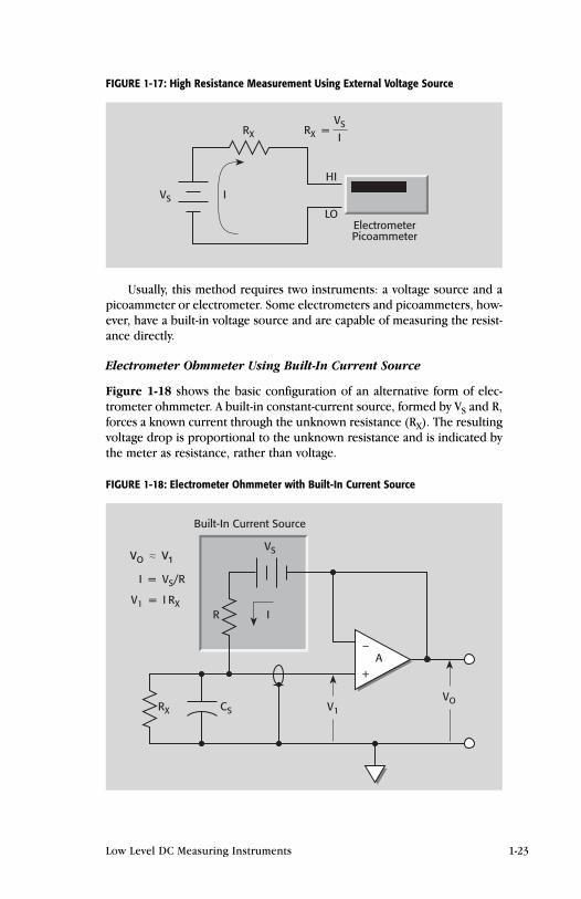
FIGURE 1-17: High Resistance Measurement Using External Voltage Source
Usually, this method requires two instruments: a voltage source and apicoammeter or electrometer. Some electrometers and picoammeters, how-ever, have a built-in voltage source and are capable of measuring the resist-ance directly.
Electrometer Ohmmeter Using Built-In Current Source
Figure 1-18 shows the basic configuration of an alternative form of elec-trometer ohmmeter. A built-in constant-current source, formed by VS and R,forces a known current through the unknown resistance (RX). The resultingvoltage drop is proportional to the unknown resistance and is indicated bythe meter as resistance, rather than voltage.
FIGURE 1-18: Electrometer Ohmmeter with Built-In Current Source
–
+A
Built-In Current Source
RX CS V1
R I
VO
I = VS/R
V1 = I RX
VS
ElectrometerPicoammeter
VS
RX
I
RX =VS
I
HI
LO
Low Level DC Measuring Instruments 1-23
The disadvantage of this method is that the voltage across the unknownis a function of its resistance, so it cannot be easily controlled. Very highresistances tend to have large voltage coefficients; therefore, measurementsmade with a constant voltage are more meaningful. In addition, theresponse speed for resistances greater than 10GΩ will be rather slow. Thislimitation can be partially overcome by guarding.
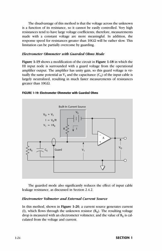
Electrometer Ohmmeter with Guarded Ohms Mode
Figure 1-19 shows a modification of the circuit in Figure 1-18 in which theHI input node is surrounded with a guard voltage from the operationalamplifier output. The amplifier has unity gain, so this guard voltage is vir-tually the same potential as V1 and the capacitance (CS) of the input cable islargely neutralized, resulting in much faster measurements of resistancesgreater than 10GΩ.
FIGURE 1-19: Electrometer Ohmmeter with Guarded Ohms
The guarded mode also significantly reduces the effect of input cableleakage resistance, as discussed in Section 2.4.2.
Electrometer Voltmeter and External Current Source
In this method, shown in Figure 1-20, a current source generates current(I), which flows through the unknown resistor (RX). The resulting voltagedrop is measured with an electrometer voltmeter, and the value of RX is cal-culated from the voltage and current.
–
+A
Built-In Current Source
RX CS V1
R I
VO
I = VS/R
V1 = I RX
VS
Guard
1-24 SECTION 1

FIGURE 1-20: High Resistance Measurement Using External Current Source withElectrometer Voltmeter
If the current source has a buffered ×1 output, a low impedance volt-meter, such as a DMM, may be used to read the voltage across RX. Thisarrangement is shown in Figure 1-21.
FIGURE 1-21: High Resistance Measurement Using a True Current Source with a DMM
1.5.5 Low Resistance Ohmmeter Circuits
Nanovoltmeter and External Current Source
If the electrometer in Figure 1-20 is replaced with a nanovoltmeter, the cir-cuit can be used to measure very low resistances (<µΩ). Using a four-wiremethod eliminates any lead resistance from the measurement. A currentsource that can automatically change polarity can be used to correct for off-sets. First, a voltage measurement is taken with positive test current, thenanother voltage measurement is taken with negative test current. Averagingthe difference between the two readings cancels the offsets.
DMM
RX
–
+
I V1
Constant-Current Sourcewith Buffered ×1 Output
VO
×1 Output
VO ≈ V1 = I RX
A
HI
LO
ElectrometerVoltmeter
I V1RX
V1 = I RX
ExternalCurrentSource
HI
LO
Low Level DC Measuring Instruments 1-25

DMM Ohmmeter
The typical DMM uses the ratiometric technique shown in Figure 1-22 tomake resistance measurements. When the resistance function is selected, aseries circuit is formed between the ohms voltage source, a reference resist-ance (RREF), and the resistance being measured (RX). The voltage causes acurrent to flow through the two resistors. This current is common to bothresistances, so the value of the unknown resistance can be determined bymeasuring the voltage across the reference resistance and across theunknown resistance and calculating as:
SENSE HI – SENSE LORX = RREF · __________________________
REF HI – REF LO
FIGURE 1-22: Ratiometric Resistance Measurement
The resistors (RS) provide automatic two-wire or four-wire resistancemeasurements. When used in the two-wire mode, the measurement willinclude the lead resistance, represented by R1 and R4. When the unknownresistance is low, perhaps less than 100Ω, the four-wire mode will give muchbetter accuracy. The sense lead resistance, R2 and R3, won’t cause significanterror because the sense circuit has very high impedance.
RX = RREFVSENSE
VREF
R1, R 2, R 3, R 4 = lead resistance
VREFRREF
RS
RS
Ref HI
Ref LO
VSENSE
Sense HI
Sense LO
Input HI
Sense HI
Sense LO
Input LOR4
R3
R2
R1
RX
Four-wireconnection
only
1-26 SECTION 1
Low Level DC Measuring Instruments 1-27
Micro-ohmmeter
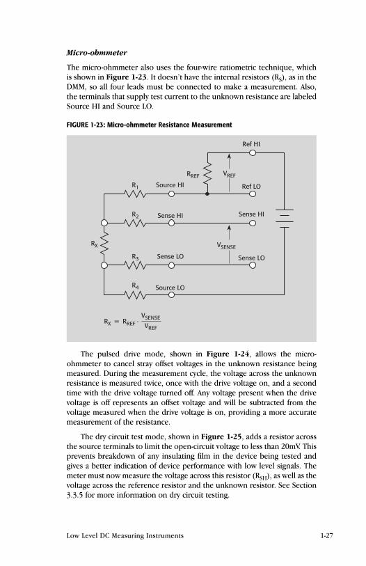
The micro-ohmmeter also uses the four-wire ratiometric technique, whichis shown in Figure 1-23. It doesn’t have the internal resistors (RS), as in theDMM, so all four leads must be connected to make a measurement. Also,the terminals that supply test current to the unknown resistance are labeledSource HI and Source LO.
FIGURE 1-23: Micro-ohmmeter Resistance Measurement
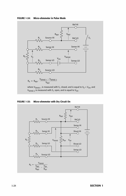
The pulsed drive mode, shown in Figure 1-24, allows the micro-ohmmeter to cancel stray offset voltages in the unknown resistance beingmeasured. During the measurement cycle, the voltage across the unknownresistance is measured twice, once with the drive voltage on, and a secondtime with the drive voltage turned off. Any voltage present when the drivevoltage is off represents an offset voltage and will be subtracted from thevoltage measured when the drive voltage is on, providing a more accuratemeasurement of the resistance.
The dry circuit test mode, shown in Figure 1-25, adds a resistor acrossthe source terminals to limit the open-circuit voltage to less than 20mV. Thisprevents breakdown of any insulating film in the device being tested andgives a better indication of device performance with low level signals. Themeter must now measure the voltage across this resistor (RSH), as well as thevoltage across the reference resistor and the unknown resistor. See Section3.3.5 for more information on dry circuit testing.
RX = RREF ·VSENSE
VREF
VREFRREF
Ref HI
Ref LO
VSENSE
Sense HI
Sense LO
Source HI
Sense HI
Sense LO
Source LOR4
R3
R2
R1
RX
1-28 SECTION 1
FIGURE 1-24: Micro-ohmmeter in Pulse Mode
RX = RREF ·VSENSE 1 – VSENSE 2
VREF
VREFRREF
Ref HI
Ref LO
VSENSE
Sense HI
Sense LO
Source HI
Sense HI
Sense LO
Source LOR4
R3
R2
R1
RX VXVOS
S1
where VSENSE 1 is measured with S1 closed, and is equal to VX + VOS, and
VSENSE 2 is measured with S1 open, and is equal to VOS.
VREFRREF
Ref HI
Ref LO
VSH
Shunt HI
Shunt LO
Source HI
Sense HI
Sense LO
Source LOR4
R3
R2
R1
RX
Sense LO
Sense HI
RSHVSENSE
RX =VSENSE
VREF
RREF
VSH
RSH
FIGURE 1-25: Micro-ohmmeter with Dry Circuit On
1.5.6 Complete Instruments
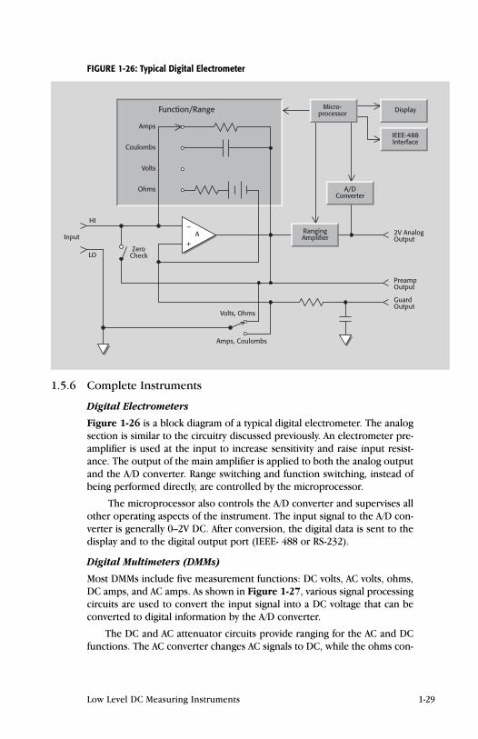
Digital Electrometers
Figure 1-26 is a block diagram of a typical digital electrometer. The analogsection is similar to the circuitry discussed previously. An electrometer pre-amplifier is used at the input to increase sensitivity and raise input resist-ance. The output of the main amplifier is applied to both the analog outputand the A/D converter. Range switching and function switching, instead ofbeing performed directly, are controlled by the microprocessor.
The microprocessor also controls the A/D converter and supervises allother operating aspects of the instrument. The input signal to the A/D con-verter is generally 0–2V DC. After conversion, the digital data is sent to thedisplay and to the digital output port (IEEE- 488 or RS-232).
Digital Multimeters (DMMs)
Most DMMs include five measurement functions: DC volts, AC volts, ohms,DC amps, and AC amps. As shown in Figure 1-27, various signal processingcircuits are used to convert the input signal into a DC voltage that can beconverted to digital information by the A/D converter.
The DC and AC attenuator circuits provide ranging for the AC and DCfunctions. The AC converter changes AC signals to DC, while the ohms con-
Low Level DC Measuring Instruments 1-29
RangingAmplifier
ZeroCheck
–
+
HI
A
Amps
Coulombs
Volts
Ohms
Function/Range
Volts, Ohms
Amps, Coulombs
LO
Input2V AnalogOutput
PreampOutput
GuardOutput
Micro-processor
A/DConverter
Display
IEEE-488Interface
FIGURE 1-26: Typical Digital Electrometer

verter provides a DC analog signal for resistance measurements. Precisionshunts are used to convert currents to voltages for the amps functions.
Once the input signal is appropriately processed, it’s converted to digi-tal information by the A/D converter. Digital data is then sent to the displayand to the digital output port (IEEE-488, RS-232, or Ethernet).
Nanovoltmeters
A nanovoltmeter is a sensitive voltmeter optimized to measure very low volt-ages. As shown in Figure 1-28, the nanovoltmeter incorporates a low noisepreamplifier, which amplifies the signal to a level suitable for A/D conver-sion (typically 2–3V full scale). Specially designed preamplifier circuitsensure that unwanted noise, thermoelectric EMFs, and offsets are kept to anabsolute minimum.
FIGURE 1-28: Typical Nanovoltmeter
1-30 SECTION 1
ACAttenuator
DCAttenuator
ACConverter
OhmsConverter
AC
DC
Ohms
AC
DC
Ohms
DigitalDisplay
A/DConverter
PrecisionReference
DigitalOutputPorts(IEEE-488,RS-232,Ethernet)
PrecisionShunts
HI
Amps
LO
INPUT
OffsetCompensation
Low-NoisePreamplifier
A/DConverter
RangeSwitching
Microprocessor
Display
IEEE-488,RS-232
DCV Input
HI
LO
FIGURE 1-27: DMM Block Diagram
Low Level DC Measuring Instruments 1-31
In order to cancel internal offsets, an offset or drift compensation cir-cuit allows the preamplifier offset voltage to be measured during specificphases of the measurement cycle. The resulting offset voltage is subse-quently subtracted from the measured signal to maximize measurementaccuracy.
Once the preamplifier amplifies the signal, it’s converted to digitalinformation by the A/D converter. Digital data is then sent to the display andthe IEEE-488 interface.
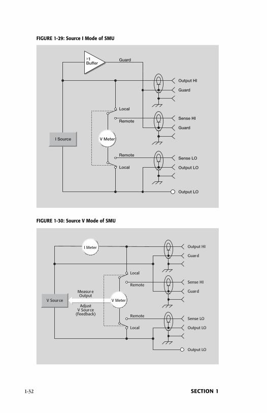
SMUs
The SMU provides four functions in one instrument: measure voltage, meas-ure current, source voltage and source current. Generally, such instrumentscan simultaneously source voltage and measure current or simultaneouslysource current and measure voltage.
When configured to Source I and Measure V (as shown in Figure 1-29),the SMU will function as a high impedance current source with voltagemeasure (and voltage limit) capability.
Selecting either local or remote sense determines where the voltagemeasurement will be made. In local sense, the voltage is measured at theoutput of the SMU. In remote sense, the voltage is measured at the deviceunder test, eliminating any voltage drops due to lead resistance.
The driven guard (×1 Buffer) ensures that the Guard and Output HI ter-minals are always at the same potential. Proper use of Guard virtually elim-inates leakage paths in the cable, test fixture, and connectors. When config-ured to Source V and Measure I (as shown in Figure 1-30), the SMU willfunction as a low impedance voltage source with current measure (and cur-rent limit) capability.
SourceMeter Instrument
Like an SMU, a SourceMeter instrument can source current, source voltage,measure current and measure voltage. However, the SourceMeter instru-ment also has a sixth terminal, guard sense, which allows making moreaccurate measurements of networks. When configured to source current asshown in Figure 1-31, the SourceMeter unit functions as a high impedancecurrent source with voltage limit capability and it can measure current, volt-age, or resistance.
For voltage measurements, the sense selection (two-wire local or four-wire remote) determines where the measurement is made. In local sense,voltage is measured at the IN/OUT terminals of the instrument. In four-wireremote sense, voltage is measured directly at the device under test using theSense terminals. This eliminates any voltage drops due to lead resistance.
When configured to source voltage as shown in Figure 1-32, theSourceMeter instrument functions as a low impedance voltage source withcurrent limit capability and it can measure current, voltage, or resistance.
1-32 SECTION 1
FIGURE 1-30: Source V Mode of SMU
FIGURE 1-29: Source I Mode of SMU
V Meter
Local
Remote
Local
Remote
Guard
Guard
Output LO
V Source
Output LO
I Meter
Measur eOutput
AdjustV Source
(Feedback)
Output HI
Sense HI
Sense LO
×1Buffer
Guard
V Meter
Local
Remote
Local
Remote
Guard
Guard
Output LO
I Source
Output LO
Output HI
Sense HI
Sense LO

Sense circuitry is used to monitor the output voltage continuously andadjust the V Source as needed.
Low Level DC Measuring Instruments 1-33
Guard
V Meter
Local
Remote
Local
Remote
In/Out HI
Sense HI
Sense LO
V Source
In/Out LO
I Meter
Guard Sense
+
–
SenseOutput
AdjustV Source
(Feedback)
FIGURE 1-31: Source I Mode of a SourceMeter Instrument
FIGURE 1-32: Source V Mode of a SourceMeter Instrument
×1 Guard
V Meter
Local
Remote
Local
Remote
In/Out HI
Sense HI
Sense LO
I Source
In/Out LO
I Meter
Guard Sense
+
–


S E C T I O N 2
Measurements fromHigh Resistance
Sources
2.1 IntroductionAs described in Section 1 of this handbook, measurements made from highresistance sources include low DC voltage, low DC current, high resistance,and charge measurements. The instruments used to make these highimpedance measurements include electrometers, picoammeters, andsource-measure units (SMUs). While Section 1 described the basic circuitsof these instruments and their measurement functions, Section 2 offersmore detailed information about these functions, various interferences anderror sources, and ways to maximize the accuracy of measurements madefrom high resistance sources. For easier reference, the information inSection 2 is organized into these subsections:
2.2 High Impedance Voltage Measurements: A discussion of loading errorsand the use of guarding to minimize these errors, as well as informationon insulating materials used for making high impedance measure-ments.
2.3 Low Current Measurements: Information about making successful lowcurrent measurements is described with such topics as leakage currentand guarding, noise and source impedance, zero drift, generated cur-rents, voltage burden, overload protection, and using a coulombmeterto measure low current.
2.4 High Resistance Measurements: Describes the constant-voltage andconstant-current methods for measuring high resistance. It alsoincludes information on high valued resistors.
2.5 Charge Measurements: A discussion of the error sources and ways tominimize them, zero check, and extending the range of the charge func-tion.
2.6 General Electrometer Considerations: A discussion of techniques anderror sources that affect high impedance measurements in general.Some of the topics include measurement connections, electrostaticinterference and shielding, environmental factors, speed considera-tions, etc.
2.2 Voltage Measurements from High Resistance SourcesMeasurements from voltage sources with high internal resistance are sub-ject to a number of errors, such as loading errors from the voltmeter’s inputresistance and input bias current, as well as from external shunt resistanceand capacitance. The following paragraphs discuss these error sources andways to minimize their effects. For a discussion of errors due to improperconnections and electrostatic interference, see Section 2.6.
2.2.1 Loading Errors and GuardingInput Resistance Loading
Voltage measurements from high resistance sources are subject to loadingerrors from the meter input resistance, as well as the leakage resistance of
2-2 SECTION 2
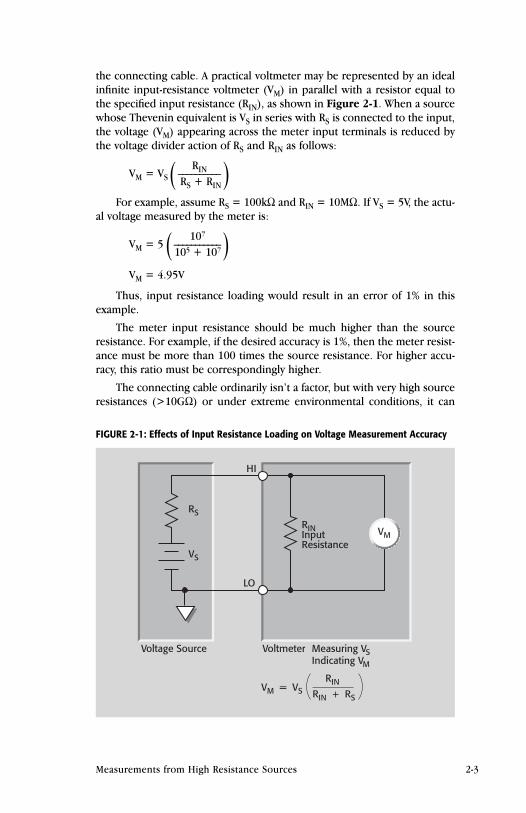
the connecting cable. A practical voltmeter may be represented by an idealinfinite input-resistance voltmeter (VM) in parallel with a resistor equal tothe specified input resistance (RIN), as shown in Figure 2-1. When a sourcewhose Thevenin equivalent is VS in series with RS is connected to the input,the voltage (VM) appearing across the meter input terminals is reduced bythe voltage divider action of RS and RIN as follows:
RINVM = VS ––––––––––( RS + RIN )
For example, assume RS = 100kΩ and RIN = 10MΩ. If VS = 5V, the actu-al voltage measured by the meter is:
107
VM = 5 –––––––––––( 105 + 107 )VM = 4.95V
Thus, input resistance loading would result in an error of 1% in thisexample.
The meter input resistance should be much higher than the sourceresistance. For example, if the desired accuracy is 1%, then the meter resist-ance must be more than 100 times the source resistance. For higher accu-racy, this ratio must be correspondingly higher.
The connecting cable ordinarily isn’t a factor, but with very high sourceresistances (>10GΩ) or under extreme environmental conditions, it can
Measurements from High Resistance Sources 2-3
VS
RS
Voltage Source
RINInputResistance
VM
HI
LO
Voltmeter Measuring VSIndicating VM
VM = VSRIN
RIN + RS
FIGURE 2-1: Effects of Input Resistance Loading on Voltage Measurement Accuracy
cause significant loading errors. It may be possible to guard the cable andthus reduce its loading on the measurement. This is discussed in the para-graphs on Shunt Resistance Loading and Guarding.
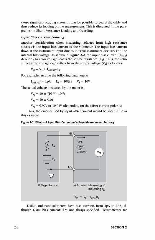
Input Bias Current Loading
Another consideration when measuring voltages from high resistancesources is the input bias current of the voltmeter. The input bias currentflows at the instrument input due to internal instrument circuitry and theinternal bias voltage. As shown in Figure 2-2, the input bias current (IBIAS)develops an error voltage across the source resistance (RS). Thus, the actu-al measured voltage (VM) differs from the source voltage (VS) as follows:
VM = VS ± IOFFSETRS
For example, assume the following parameters:
IOFFSET = 1pA RS = 10GΩ VS = 10V
The actual voltage measured by the meter is:
VM = 10 ± (10–12 · 1010)
VM = 10 ± 0.01
VM = 9.99V or 10.01V (depending on the offset current polarity)
Thus, the error caused by input offset current would be about 0.1% inthis example.
Figure 2-2: Effects of Input Bias Current on Voltage Measurement Accuracy
DMMs and nanovoltmeters have bias currents from 1pA to 1nA, al-though DMM bias currents are not always specified. Electrometers are
VS
RS
Voltage Source
IBIAS
InputBiasCurrent VM
HI
LO
Voltmeter Measuring VSIndicating VM
VM = VS – IBIAS RS
2-4 SECTION 2

known for their low input bias current, which is usually a few femtoamps.Picoammeters and SMUs also have very low input bias currents, althoughusually not as low as an electrometer’s.
Although input bias current is a common source of this type of error,currents generated by external circuits can also result in errors due to volt-age drops across the source resistance. Typical sources of such offset cur-rents are insulators and cables.
Shunt Resistance Loading and Guarding
External shunt resistances, such as leaky cables and dirty insulators, mayalso cause loading errors.
Any external shunt resistance across the voltage source will attenuatethe measured voltage, as shown in Figure 2-3. As in the case of input resist-ance voltage loading, the shunt resistance (RSHUNT) and the source resist-ance (RS) form a voltage divider that reduces the measured voltage (VM) asfollows:
RSHUNTVM = VS ––––––––––––––( RSHUNT + RS)
For example, assume RS = 10GΩ and RSHUNT = 100GΩ. If VS has a valueof 10V, the measured voltage (VM) is:
1011
VM = 10 ––––––––––––( 1011 + 1010 )VM = 9.09V
In this instance, the error due to shunt loading is approximately 9%.
Measurements from High Resistance Sources 2-5
VS
RS
Voltage Source
RSHUNT VM
HI
LO
Voltmeter Measuring VSIndicating VM
VM = VSRSHUNT
RS + RSHUNT
ShuntResistance
FIGURE 2-3: Effects of Shunt Resistance on Voltage Measurement Accuracy
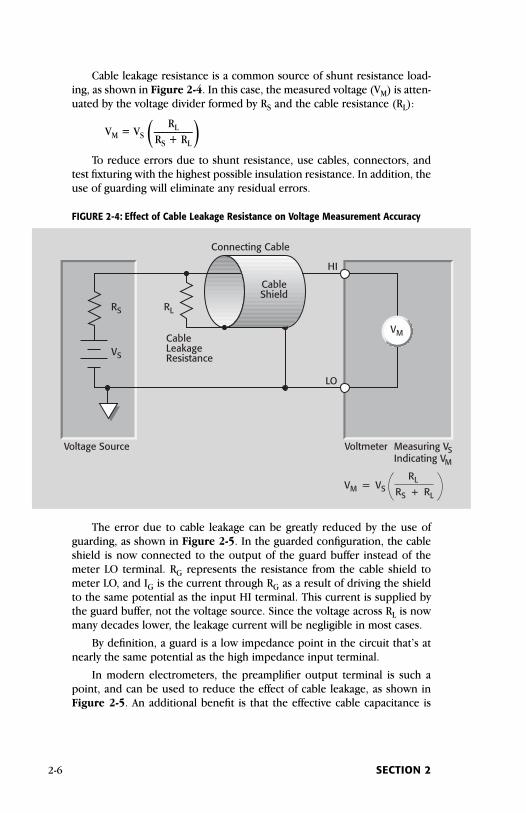
Cable leakage resistance is a common source of shunt resistance load-ing, as shown in Figure 2-4. In this case, the measured voltage (VM) is atten-uated by the voltage divider formed by RS and the cable resistance (RL):
RLVM = VS –––––––––( RS + RL)
To reduce errors due to shunt resistance, use cables, connectors, andtest fixturing with the highest possible insulation resistance. In addition, theuse of guarding will eliminate any residual errors.
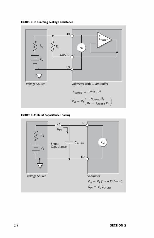
The error due to cable leakage can be greatly reduced by the use ofguarding, as shown in Figure 2-5. In the guarded configuration, the cableshield is now connected to the output of the guard buffer instead of themeter LO terminal. RG represents the resistance from the cable shield tometer LO, and IG is the current through RG as a result of driving the shieldto the same potential as the input HI terminal. This current is supplied bythe guard buffer, not the voltage source. Since the voltage across RL is nowmany decades lower, the leakage current will be negligible in most cases.
By definition, a guard is a low impedance point in the circuit that’s atnearly the same potential as the high impedance input terminal.
In modern electrometers, the preamplifier output terminal is such apoint, and can be used to reduce the effect of cable leakage, as shown inFigure 2-5. An additional benefit is that the effective cable capacitance is
2-6 SECTION 2
VS
RS
Voltage Source
RL
VM
HI
LO
Voltmeter Measuring VSIndicating VM
VM = VSRL
RS + RL
CableLeakageResistance
Connecting Cable
CableShield
FIGURE 2-4: Effect of Cable Leakage Resistance on Voltage Measurement Accuracy
also reduced, making the response speed of the circuit much faster. This isdiscussed in detail in the paragraphs on Shunt Capacitance Loading andGuarding.
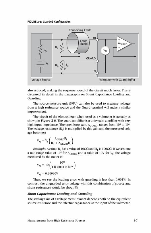
The source-measure unit (SMU) can also be used to measure voltagesfrom a high resistance source and the Guard terminal will make a similarimprovement.
The circuit of the electrometer when used as a voltmeter is actually asshown in Figure 2-6. The guard amplifier is a unity-gain amplifier with veryhigh input impedance. The open-loop gain, AGUARD, ranges from 104 to 106.The leakage resistance (RL) is multiplied by this gain and the measured volt-age becomes:
AGUARDRLVM = VS –––––––––––––––––( RS + AGUARDRL)
Example: Assume RS has a value of 10GΩ and RL is 100GΩ. If we assumea mid-range value of 105 for AGUARD and a value of 10V for VS, the voltagemeasured by the meter is:
1016
VM = 10 ––––––––––––––––––( 1.000001 × 10¹⁶ )VM = 9.99999V
Thus, we see the loading error with guarding is less than 0.001%. Incontrast, the unguarded error voltage with this combination of source andshunt resistances would be about 9%.
Shunt Capacitance Loading and Guarding
The settling time of a voltage measurement depends both on the equivalentsource resistance and the effective capacitance at the input of the voltmeter;
Measurements from High Resistance Sources 2-7
+
–
Voltage Source
RLVM
GUARD
LO
Voltmeter with Guard Buffer
RG IG
HI
Connecting Cable
CableShield
RS
VS
AGUARD
FIGURE 2-5: Guarded Configuration
2-8 SECTION 2
FIGURE 2-7: Shunt Capacitance Loading
VS
RS
Voltage Source
CSHUNTVM
HI
LO
Voltmeter
VM = VS (1 – e–t/RSCSHUNT)
ShuntCapacitance
QIN
QIN = VS CSHUNT
FIGURE 2-6: Guarding Leakage Resistance
+
–
VS
RS
Voltage Source
RL VM
HI
LO
Voltmeter with Guard Buffer
AGUARD =
AGUARD
VM = VSAGUARD RL
RS + AGUARD RL
104 to 106
GUARD
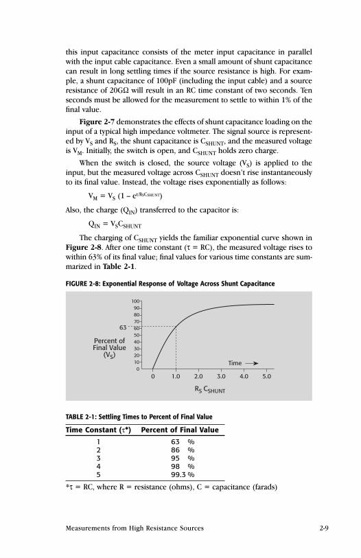
this input capacitance consists of the meter input capacitance in parallelwith the input cable capacitance. Even a small amount of shunt capacitancecan result in long settling times if the source resistance is high. For exam-ple, a shunt capacitance of 100pF (including the input cable) and a sourceresistance of 20GΩ will result in an RC time constant of two seconds. Tenseconds must be allowed for the measurement to settle to within 1% of thefinal value.
Figure 2-7 demonstrates the effects of shunt capacitance loading on theinput of a typical high impedance voltmeter. The signal source is represent-ed by VS and RS, the shunt capacitance is CSHUNT, and the measured voltageis VM. Initially, the switch is open, and CSHUNT holds zero charge.
When the switch is closed, the source voltage (VS) is applied to theinput, but the measured voltage across CSHUNT doesn’t rise instantaneouslyto its final value. Instead, the voltage rises exponentially as follows:
VM = VS (1 – et/RSCSHUNT)
Also, the charge (QIN) transferred to the capacitor is:
QIN = VSCSHUNT
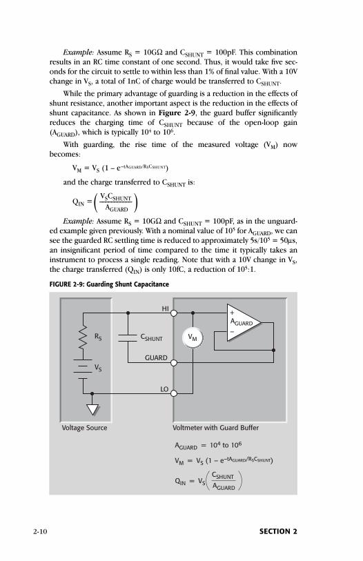
The charging of CSHUNT yields the familiar exponential curve shown inFigure 2-8. After one time constant (τ = RC), the measured voltage rises towithin 63% of its final value; final values for various time constants are sum-marized in Table 2-1.
TABLE 2-1: Settling Times to Percent of Final Value
Time Constant (τ*) Percent of Final Value
1 63 %2 86 %3 95 %4 98 %5 99.3 %
*τ = RC, where R = resistance (ohms), C = capacitance (farads)
Measurements from High Resistance Sources 2-9
FIGURE 2-8: Exponential Response of Voltage Across Shunt Capacitance
Time
100
0 1.0 2.0 3.0 4.0 5.0
63
RS CSHUNT
90807060
403020
50
100
Percent ofFinal Value
(VS)
Example: Assume RS = 10GΩ and CSHUNT = 100pF. This combinationresults in an RC time constant of one second. Thus, it would take five sec-onds for the circuit to settle to within less than 1% of final value. With a 10Vchange in VS, a total of 1nC of charge would be transferred to CSHUNT.
While the primary advantage of guarding is a reduction in the effects ofshunt resistance, another important aspect is the reduction in the effects ofshunt capacitance. As shown in Figure 2-9, the guard buffer significantlyreduces the charging time of CSHUNT because of the open-loop gain(AGUARD), which is typically 104 to 106.
With guarding, the rise time of the measured voltage (VM) nowbecomes:
VM = VS (1 – e–tAGUARD/RSCSHUNT)
and the charge transferred to CSHUNT is:
VSCSHUNTQIN = –––––––––––( AGUARD)
Example: Assume RS = 10GΩ and CSHUNT = 100pF, as in the unguard-ed example given previously. With a nominal value of 105 for AGUARD, we cansee the guarded RC settling time is reduced to approximately 5s/105 = 50µs,an insignificant period of time compared to the time it typically takes aninstrument to process a single reading. Note that with a 10V change in VS,the charge transferred (QIN) is only 10fC, a reduction of 105:1.
2-10 SECTION 2
FIGURE 2-9: Guarding Shunt Capacitance
QIN = VS AGUARD
CSHUNT
+
–
VS
RS
Voltage Source
CSHUNT VM
HI
LO
Voltmeter with Guard Buffer
AGUARD
VM = VS (1 – e–tAGUARD/RSCSHUNT)
AGUARD = 104 to 106
GUARD
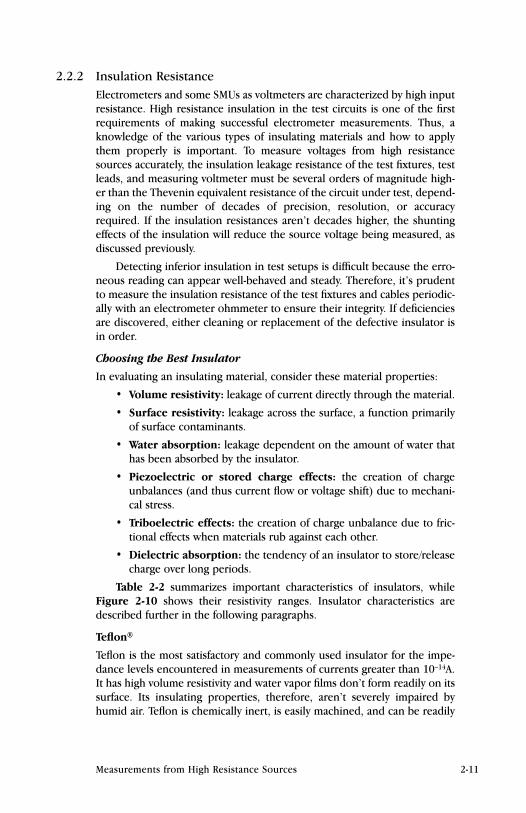
2.2.2 Insulation ResistanceElectrometers and some SMUs as voltmeters are characterized by high inputresistance. High resistance insulation in the test circuits is one of the firstrequirements of making successful electrometer measurements. Thus, aknowledge of the various types of insulating materials and how to applythem properly is important. To measure voltages from high resistancesources accurately, the insulation leakage resistance of the test fixtures, testleads, and measuring voltmeter must be several orders of magnitude high-er than the Thevenin equivalent resistance of the circuit under test, depend-ing on the number of decades of precision, resolution, or accuracyrequired. If the insulation resistances aren’t decades higher, the shuntingeffects of the insulation will reduce the source voltage being measured, asdiscussed previously.
Detecting inferior insulation in test setups is difficult because the erro-neous reading can appear well-behaved and steady. Therefore, it’s prudentto measure the insulation resistance of the test fixtures and cables periodic-ally with an electrometer ohmmeter to ensure their integrity. If deficienciesare discovered, either cleaning or replacement of the defective insulator isin order.
Choosing the Best Insulator
In evaluating an insulating material, consider these material properties:
• Volume resistivity: leakage of current directly through the material.
• Surface resistivity: leakage across the surface, a function primarilyof surface contaminants.
• Water absorption: leakage dependent on the amount of water thathas been absorbed by the insulator.
• Piezoelectric or stored charge effects: the creation of chargeunbalances (and thus current flow or voltage shift) due to mechani-cal stress.
• Triboelectric effects: the creation of charge unbalance due to fric-tional effects when materials rub against each other.
• Dielectric absorption: the tendency of an insulator to store/releasecharge over long periods.
Table 2-2 summarizes important characteristics of insulators, whileFigure 2-10 shows their resistivity ranges. Insulator characteristics aredescribed further in the following paragraphs.
Teflon®
Teflon is the most satisfactory and commonly used insulator for the impe-dance levels encountered in measurements of currents greater than 10–14A.It has high volume resistivity and water vapor films don’t form readily on itssurface. Its insulating properties, therefore, aren’t severely impaired byhumid air. Teflon is chemically inert, is easily machined, and can be readily
Measurements from High Resistance Sources 2-11
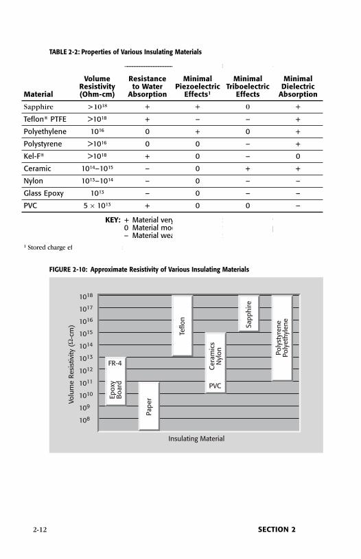
2-12 SECTION 2
1018
1017
1016
1015
1014
1013
1012
1011
1010
109
108
Insulating Material
Volu
me
Resi
stiv
ity(Ω
-cm
)
FR-4
Epox
yB
oard
Pape
r
Teflo
n
Sapp
hire
PVC
Cer
amic
sN
ylon Po
lyst
yren
ePo
lyet
hyle
ne
FIGURE 2-10: Approximate Resistivity of Various Insulating Materials
________________________________ PROPERTY ________________________________
Material
VolumeResistivity(Ohm-cm)
Resistanceto Water
Absorption
MinimalPiezoelectric
Effects1
MinimalTriboelectric
Effects
MinimalDielectric
Absorption
Sapphire >1018 + + 0 +
Teflon® PTFE >1018 + – – +
Polyethylene 1016 0 + 0 +
Polystyrene >1016 0 0 – +
Kel-F® >1018 + 0 – 0
Ceramic 1014–1015 – 0 + +
Nylon 1013–1014 – 0 – –
Glass Epoxy 1013 – 0 – –
PVC 5 × 10¹³ + 0 0 –
KEY: + Material very good in regard to the property.0 Material moderately good in regard to the property.– Material weak in regard to the property.
1 Stored charge effects in non-piezoelectric insulators.
TABLE 2-2: Properties of Various Insulating Materials
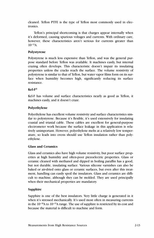
cleaned. Teflon PTFE is the type of Teflon most commonly used in elec-tronics.
Teflon’s principal shortcoming is that charges appear internally whenit’s deformed, causing spurious voltages and currents. With ordinary care,however, these characteristics aren’t serious for currents greater than10–13A.
Polystyrene
Polystyrene is much less expensive than Teflon, and was the general pur-pose standard before Teflon was available. It machines easily, but internalcrazing often develops. This characteristic doesn’t impair its insulatingproperties unless the cracks reach the surface. The volume resistivity ofpolystyrene is similar to that of Teflon, but water vapor films form on its sur-face when humidity becomes high, significantly reducing its surfaceresistance.
Kel-F®
Kel-F has volume and surface characteristics nearly as good as Teflon, itmachines easily, and it doesn’t craze.
Polyethylene
Polyethylene has excellent volume resistivity and surface characteristics sim-ilar to polystyrene. Because it’s flexible, it’s used extensively for insulatingcoaxial and triaxial cable. These cables are excellent for general-purposeelectrometer work because the surface leakage in this application is rela-tively unimportant. However, polyethylene melts at a relatively low temper-ature, so leads into ovens should use Teflon insulation rather than poly-ethylene.
Glass and Ceramics
Glass and ceramics also have high volume resistivity, but poor surface prop-erties at high humidity and often-poor piezoelectric properties. Glass orceramic cleaned with methanol and dipped in boiling paraffin has a good,but not durable, insulating surface. Various silicone varnishes can also bebaked or air-dried onto glass or ceramic surfaces, but even after this treat-ment, handling can easily spoil the insulators. Glass and ceramics are diffi-cult to machine, although they can be molded. They are used principallywhen their mechanical properties are mandatory.
Sapphire
Sapphire is one of the best insulators. Very little charge is generated in itwhen it’s stressed mechanically. It’s used most often in measuring currentsin the 10–18A to 10–15A range. The use of sapphire is restricted by its cost andbecause the material is difficult to machine and form.
Measurements from High Resistance Sources 2-13
Quartz
Quartz has properties similar to sapphire, but considerably higher piezo-electric output, so it’s rarely used in electrometer circuits.
Other Insulating Materials
Practically all other insulating materials have unacceptably low volumeresistivity or unsatisfactory surface characteristics for electrometer use.Vinyl, nylon, and Lucite® are markedly inferior to Teflon, polystyrene, poly-ethylene, sapphire, or quartz.
Keeping Insulators Clean
As with any high resistance device, mishandling can destroy the integrity ofinsulators. Oils and salts from the skin can degrade insulator performance,and contaminants in the air can be deposited on the insulator surface,reducing its resistance. Therefore, insulator handling should be minimized;under no circumstances should the insulator be touched with the hand orwith any material that might contaminate the surface.
If the insulator becomes contaminated, either through careless hand-ling or from deposits, it can be cleaned with a foam tipped swab dipped inmethanol. After cleaning, the insulator should be allowed to dry for severalhours at low humidity before use or be dried using dry nitrogen.
2.3 Low Current MeasurementsA number of error sources can have serious impacts on low current meas-urement accuracy. For example, the ammeter may cause measurementerrors if not connected properly. (Refer to Sections 2.6.1 and 2.6.2 for moreinformation on how to make properly shielded connections.) The amme-ter’s voltage burden and input offset current may also affect measurementaccuracy. The source resistance of the device under test will affect the noiseperformance of a feedback ammeter. External sources of error can includeleakage current from cables and fixtures, as well as currents generated bytriboelectric or piezoelectric effects. Section 2.3 addresses low currentmeasurement considerations in detail and outlines methods for minimizingthe effects of error sources. It also includes information on using the elec-trometer’s coulomb function to make very low current measurements.
2.3.1 Leakage Currents and GuardingLeakage currents are generated by stray resistance paths between the meas-urement circuit and nearby voltage sources. These currents can degrade theaccuracy of low current measurements considerably. To reduce leakage cur-rents, use good quality insulators, reduce the level of humidity in the testenvironment, and use guarding. Guarding will also reduce the effect ofshunt capacitance in the measurement circuit.
Using good quality insulators when building the test circuit is one wayto reduce leakage currents. Teflon, polyethylene, and sapphire are examples
2-14 SECTION 2
of good quality insulators, but avoid materials like phenolics and nylon.Refer to Section 2.2.2 for further discussion on choosing the best insulatingmaterials.
Humidity may also degrade low current measurements. Different typesof insulators will absorb varying amounts of water from the air, so it’s bestto choose an insulator on which water vapor doesn’t readily form a contin-uous film. Sometimes, this is unavoidable if the material being measuredabsorbs water easily, so it’s best to make the measurements in an environ-mentally controlled room. In some cases, an insulator may have ioniccontaminants, which can generate a spurious current, especially in highhumidity.
Guarding is a very effective way to reduce leakage currents. A guard is alow impedance point in the circuit that’s at nearly the same potential as thehigh impedance lead being guarded. The guard on the electrometer amme-ter and picoammeter differs from the guard on the SMU ammeter. The useof guarding can best be explained through examples.
The Use of Guarding Using an Electrometer Ammeter orPicoammeter
The guard terminal of the electrometer ammeter or picoammeter is the LOinput terminal. The guard can be used to isolate the high impedance inputlead of the ammeter from leakage current due to voltage sources. Figures2-11 and 2-12 illustrate examples of guarding.
Figure 2-11 illustrates guarding as applied to measuring the ion cur-rent (IC) from an ionization chamber. An unguarded ionization chamberand the corresponding equivalent circuit are shown in Figure 2-11a. Theequivalent circuit shows that the full bias voltage appears across the insula-tor leakage resistance (RL), therefore, a leakage current (IL) will be added tothe measured ion current (IM = IC + IL). The leakage resistance is due tothe insulator of the ionization chamber and the coax cable.
In Figure 2-11b, a metal guard ring is added to the ionization chamber.This guard circuit splits the leakage resistance into two parts. The voltageacross RL1 is the picoammeter voltage burden, normally less than one milli-volt, so the resulting current will be quite small. The full bias voltageappears across RL2. A leakage current will flow around this loop, but won’taffect the measurement.
Guarding may also be necessary to prevent leakage current due to testfixturing. Figure 2-12 shows a high mega-ohm resistor (RDUT) supported ontwo insulators mounted in a metal test fixture.
Figure 2-12a is the unguarded circuit. The leakage current (IL) throughthe stand-off insulators will be added to the measured current (IM).
As illustrated in Figure 2-12b, this circuit is guarded by connecting theLO of the picoammeter (IM) to the metal mounting plate. This will put thebottom of the right insulator at almost the same potential as the top. The
Measurements from High Resistance Sources 2-15
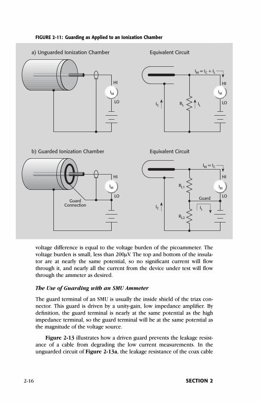
voltage difference is equal to the voltage burden of the picoammeter. Thevoltage burden is small, less than 200µV. The top and bottom of the insula-tor are at nearly the same potential, so no significant current will flowthrough it, and nearly all the current from the device under test will flowthrough the ammeter as desired.
The Use of Guarding with an SMU Ammeter
The guard terminal of an SMU is usually the inside shield of the triax con-nector. This guard is driven by a unity-gain, low impedance amplifier. Bydefinition, the guard terminal is nearly at the same potential as the highimpedance terminal, so the guard terminal will be at the same potential asthe magnitude of the voltage source.
Figure 2-13 illustrates how a driven guard prevents the leakage resist-ance of a cable from degrading the low current measurements. In theunguarded circuit of Figure 2-13a, the leakage resistance of the coax cable
2-16 SECTION 2
HI
LO
HI
LO
HI
LO
HI
LO
GuardConnection
Guard
RL
IM IM
a) Unguarded Ionization Chamber Equivalent Circuit
IL
RL1IM
RL2
IM
b) Guarded Ionization Chamber Equivalent Circuit
IL
IC
IM = IC + IL
IC
IM = IC
FIGURE 2-11: Guarding as Applied to an Ionization Chamber

is in parallel with the DUT (RDUT), creating an unwanted leakage current(IL). This leakage current will degrade very low current measurements.
In the guarded circuit shown in Figure 2-13b, the inside shield of thetriax cable is connected to the guard terminal of the SMU. Now this shieldis driven by a unity-gain, low impedance amplifier (Guard). The difference
Measurements from High Resistance Sources 2-17
V
Metal Shielded Test Fixture
IDUT
HI
IM
LO
Connection forElectrostatic Shielding
Standoff
HI
LO
IM = IDUT + IL
RDUT
RL RL
Metal Mounting Plate
IL
a) Unguarded Circuit
V
Metal Shielded Test Fixture
IDUT
HI
IM
LO
Shield Connection(LO Terminal toMetal Shield of
Test Fixture)
Standoff
HI
LO
IM = IDUT
RDUT
RL RL
Metal Mounting PlateIL
b) Guarded Circuit
Guard Connection(LO Terminal toMetal Mounting
Plate)
0V
FIGURE 2-12: Guarding to Reduce Leakage Currents
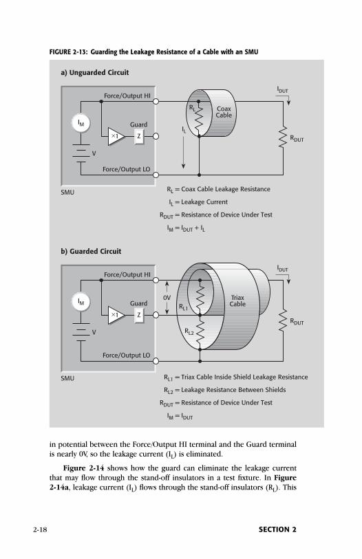
2-18 SECTION 2
RL = Coax Cable Leakage Resistance
IL = Leakage Current
RDUT = Resistance of Device Under Test
IM = IDUT + IL
V
SMU
RL
Z
a) Unguarded Circuit
Force/Output HI
CoaxCable
RDUT
IM
IDUT
×1
Force/Output LO
ILGuard
RL1 = Triax Cable Inside Shield Leakage Resistance
RL2 = Leakage Resistance Between Shields
RDUT = Resistance of Device Under Test
IM = IDUT
V
SMU
RL1Z
b) Guarded Circuit
Force/Output HI
TriaxCable
RDUT
IM
IDUT
×1
Force/Output LO
0VGuard
RL2
FIGURE 2-13: Guarding the Leakage Resistance of a Cable with an SMU
in potential between the Force/Output HI terminal and the Guard terminalis nearly 0V, so the leakage current (IL) is eliminated.
Figure 2-14 shows how the guard can eliminate the leakage currentthat may flow through the stand-off insulators in a test fixture. In Figure 2-14a, leakage current (IL) flows through the stand-off insulators (RL). This
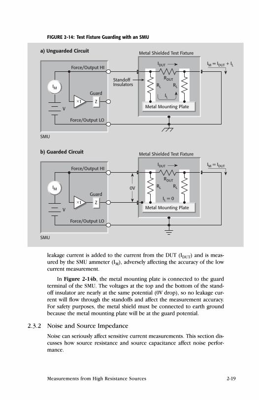
leakage current is added to the current from the DUT (IDUT) and is meas-ured by the SMU ammeter (IM), adversely affecting the accuracy of the lowcurrent measurement.
In Figure 2-14b, the metal mounting plate is connected to the guardterminal of the SMU. The voltages at the top and the bottom of the stand-off insulator are nearly at the same potential (0V drop), so no leakage cur-rent will flow through the standoffs and affect the measurement accuracy.For safety purposes, the metal shield must be connected to earth groundbecause the metal mounting plate will be at the guard potential.
2.3.2 Noise and Source Impedance
Noise can seriously affect sensitive current measurements. This section dis-cusses how source resistance and source capacitance affect noise perfor-mance.
Measurements from High Resistance Sources 2-19
Metal Shielded Test Fixture
IDUT IM = IDUT
RDUT
RL RL
Metal Mounting Plate
IL = 0
V
SMU
Z
b) Guarded Circuit
Force/Output HI
×1
Force/Output LO
0VGuard
IM
Metal Shielded Test Fixture
IDUT
StandoffInsulators
IM = IDUT + IL
RDUT
RL RL
Metal Mounting Plate
IL
V
SMU
Z
a) Unguarded Circuit
Force/Output HI
×1
Force/Output LO
Guard
IM
FIGURE 2-14: Test Fixture Guarding with an SMU
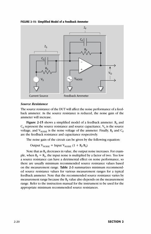
Source Resistance
The source resistance of the DUT will affect the noise performance of a feed-back ammeter. As the source resistance is reduced, the noise gain of theammeter will increase.
Figure 2-15 shows a simplified model of a feedback ammeter. RS andCS represent the source resistance and source capacitance, VS is the sourcevoltage, and VNOISE is the noise voltage of the ammeter. Finally, RF and CFare the feedback resistance and capacitance respectively.
The noise gain of the circuit can be given by the following equation:
Output VNOISE = Input VNOISE (1 + RF/RS)
Note that as RS decreases in value, the output noise increases. For exam-ple, when RF = RS, the input noise is multiplied by a factor of two. Too lowa source resistance can have a detrimental effect on noise performance, sothere are usually minimum recommended source resistance values basedon the measurement range. Table 2-3 summarizes minimum recommend-ed source resistance values for various measurement ranges for a typicalfeedback ammeter. Note that the recommended source resistance varies bymeasurement range because the RF value also depends on the measurementrange. Refer to the instruction manual for the instrument to be used for theappropriate minimum recommended source resistances.
2-20 SECTION 2
–
+
RF
CS
VS
RS
CF
VNOISE
Current Source
VO
ZF
ZS
Feedback Ammeter
FIGURE 2-15: Simplified Model of a Feedback Ammeter
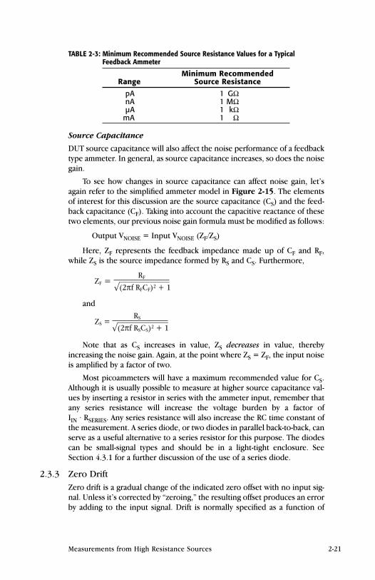
Source Capacitance
DUT source capacitance will also affect the noise performance of a feedbacktype ammeter. In general, as source capacitance increases, so does the noisegain.
To see how changes in source capacitance can affect noise gain, let’sagain refer to the simplified ammeter model in Figure 2-15. The elementsof interest for this discussion are the source capacitance (CS) and the feed-back capacitance (CF). Taking into account the capacitive reactance of thesetwo elements, our previous noise gain formula must be modified as follows:
Output VNOISE = Input VNOISE (ZF/ZS)
Here, ZF represents the feedback impedance made up of CF and RF,while ZS is the source impedance formed by RS and CS. Furthermore,
and
Note that as CS increases in value, ZS decreases in value, therebyincreasing the noise gain. Again, at the point where ZS = ZF, the input noiseis amplified by a factor of two.
Most picoammeters will have a maximum recommended value for CS.Although it is usually possible to measure at higher source capacitance val-ues by inserting a resistor in series with the ammeter input, remember thatany series resistance will increase the voltage burden by a factor of IIN · RSERIES. Any series resistance will also increase the RC time constant ofthe measurement. A series diode, or two diodes in parallel back-to-back, canserve as a useful alternative to a series resistor for this purpose. The diodescan be small-signal types and should be in a light-tight enclosure. SeeSection 4.3.1 for a further discussion of the use of a series diode.
2.3.3 Zero DriftZero drift is a gradual change of the indicated zero offset with no input sig-nal. Unless it’s corrected by “zeroing,” the resulting offset produces an errorby adding to the input signal. Drift is normally specified as a function of
ZS =RS
(2πf RSCS)2 + 1
ZF =RF
(2πf RFCF)2 + 1
Measurements from High Resistance Sources 2-21
TABLE 2-3: Minimum Recommended Source Resistance Values for a TypicalFeedback Ammeter
Minimum RecommendedRange Source Resistance
pA 1 GΩnA 1 MΩµA 1 kΩ
mA 1 Ω
time and/or temperature. Zero offset over a time period and temperaturerange will stay within the specified limits. Offset due to step changes in tem-peratures may exceed the specification before settling. Typical room tem-perature rates of change (1°C/15 minutes) won’t usually cause overshoot.
Most electrometers include a means to correct for zero drift. A ZEROCHECK switch is used to configure most electrometers and picoammetersto display any internal voltage offsets. This feature allows fast checking andadjustment of the amplifier zero. Typically, the instrument is zero correctedwhile zero check is enabled. This procedure may need to be performedperiodically, depending on ambient conditions. Electrometers perform thisfunction with the touch of a button or upon command from the computer.
In a picoammeter or electrometer ammeter, note that ZERO CHECKand ZERO CORRECT functions are used to correct for internal voltage off-sets. SUPPRESS or REL controls are used to correct for external current off-sets. For optimum accuracy, zero the instrument on the range to be used formeasurement. Refer to Section 2.3.4 for a discussion of correcting for inter-nal offset current.
2.3.4 Generated CurrentsAny extraneous generated currents in the test system will add to the desiredcurrent, causing errors. Currents can be internally generated, as in the caseof instrument input offset current, or they can come from external sourcessuch as insulators and cables. The following paragraphs discuss the varioustypes of generated currents.
Figure 2-16 summarizes the magnitudes of a number of generated cur-rents discussed in this section.
Offset Currents
Offset currents can be generated within an instrument (input offset current)or can be generated from external circuitry (external offset current).
Input Offset Current
The ideal ammeter should read zero when its input terminals are left open.Practical ammeters, however, do have some small current that flows whenthe input is open. This current is known as the input offset current, and it’scaused by bias currents of active devices as well as by leakage currentsthrough insulators within the instrument. Offset currents generated withinpicoammeters, electrometers, and SMUs are included in the instrument’sspecifications. As shown in Figure 2-17, the input offset current adds to themeasured current so the meter measures the sum of the two currents:
IM = IS + IOFFSET
Input offset current can be determined by capping the input connectorand selecting the lowest current range. Allow about five minutes for theinstrument to settle, then take a reading. This value should be within theinstrument’s specification.
2-22 SECTION 2

If an instrument has current suppression, the input offset current canbe partially nulled by enabling the current suppress function with the inputterminals disconnected and ZERO CHECK open.
Another way to subtract the input offset current from measurements isto use the relative (REL or zero) function of the ammeter. With the input
Measurements from High Resistance Sources 2-23
10–7
10–8
10–9
10–10
10–11
10–12
10–13
10–14
10–15
Standardcable
Lownoisecable
Dirtysurface
Epoxyboard
Cleansurface
Teflo
n
Cer
amic
s109Ω
1012Ω
TriboelectricEffects
ElectrochemicalEffects
MechanicalStressEffects
Resistornoise in 1Hzbandwidth
Current-Generating Phenomena
Typi
calC
urre
ntG
ener
ated
(A)
FIGURE 2-16: Typical Magnitudes of Generated Currents
FIGURE 2-17: Effects of Input Offset Current on Current Measurement Accuracy
VS
RS
IM
HI
LO
DMM, Electrometer, SMU,or PicoammeterMeasuring Current ISIndicating IM
IS
Current Source
IM = IS + IOFFSET
IOFFSET
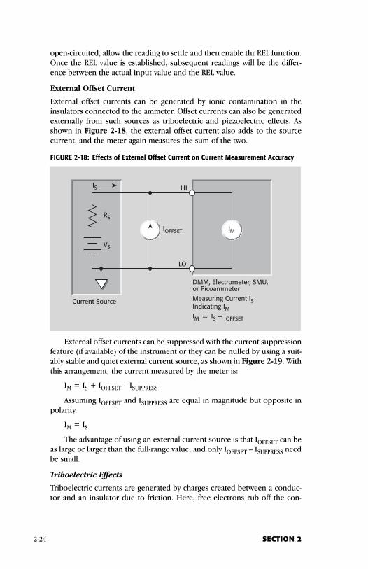
open-circuited, allow the reading to settle and then enable thr REL function.Once the REL value is established, subsequent readings will be the differ-ence between the actual input value and the REL value.
External Offset Current
External offset currents can be generated by ionic contamination in theinsulators connected to the ammeter. Offset currents can also be generatedexternally from such sources as triboelectric and piezoelectric effects. Asshown in Figure 2-18, the external offset current also adds to the sourcecurrent, and the meter again measures the sum of the two.
FIGURE 2-18: Effects of External Offset Current on Current Measurement Accuracy
External offset currents can be suppressed with the current suppressionfeature (if available) of the instrument or they can be nulled by using a suit-ably stable and quiet external current source, as shown in Figure 2-19. Withthis arrangement, the current measured by the meter is:
IM = IS + IOFFSET – ISUPPRESS
Assuming IOFFSET and ISUPPRESS are equal in magnitude but opposite inpolarity,
IM = IS
The advantage of using an external current source is that IOFFSET can beas large or larger than the full-range value, and only IOFFSET – ISUPPRESS needbe small.
Triboelectric Effects
Triboelectric currents are generated by charges created between a conduc-tor and an insulator due to friction. Here, free electrons rub off the con-
VS
RS
IM
HI
LO
DMM, Electrometer, SMU,or PicoammeterMeasuring Current ISIndicating IM
IS
Current Source
IM = IS + IOFFSET
IOFFSET
2-24 SECTION 2

ductor and create a charge imbalance that causes the current flow. A typicalexample would be electrical currents generated by insulators and conduc-tors rubbing together in a coaxial cable, as shown in Figure 2-20.
FIGURE 2-20: Triboelectric Effect
“Low noise” cable greatly reduces this effect. It typically uses an innerinsulator of polyethylene coated with graphite underneath the outer shield.The graphite provides lubrication and a conducting equipotential cylinder
IFrictional motion atboundary due tocable motion
+ +
– –
Insulation
Coaxialcable
Outerjacket
Outershield
Conductivelubricant inlow noise cable
Innerconductor
I
Measurements from High Resistance Sources 2-25
FIGURE 2-19: Using External Current Source to Suppress Offset Current
VS
RS
IM
HI
LO
DMM, Electrometer, SMU,or PicoammeterMeasuring Current ISIndicating IM
IS
Current Source
IM = IS + IOFFSET – ISUPPRESS
When IOFFSET = ISUPPRESS, IS = IM
ISUPPRESSIOFFSET
to equalize charges and minimize charge generated by frictional effects ofcable movement. However, even low noise cable creates some noise whensubjected to vibration and expansion or contraction, so all connectionsshould be kept short, away from temperature changes (which would createthermal expansion forces), and preferably supported by taping or tying thecable to a non-vibrating surface such as a wall, bench, or other rigidstructure.
There are a variety of other solutions to movement and vibration prob-lems:
• Removal or mechanical decoupling of the source of vibration.Motors, pumps, and other electromechanical devices are the usualsources.
• Stabilization of the test hookup. Securely mount or tie down elec-tronic components, wires, and cables. Shielding should be sturdy.
Triboelectric effects can also occur in other insulators and conductorsthat touch each other. Therefore, it’s important to minimize contactbetween insulators as well as conductors in constructing test fixtures andconnections for low current and high impedance.
Table 2-2 in Section 2.2.2 summarizes the triboelectric effects of vari-ous insulating materials.
Piezoelectric and Stored Charge Effects
Piezoelectric currents are generated when mechanical stress is applied tocertain crystalline materials when used for insulated terminals and inter-connecting hardware. In some plastics, pockets of stored charge cause thematerial to behave in a manner similar to piezoelectric materials. An exam-ple of a terminal with a piezoelectric insulator is shown in Figure 2-21.
To minimize the current due to this effect, it’s important to removemechanical stresses from the insulator and use insulating materials withminimal piezoelectric and stored charge effects. Section 2.2.2 and Table 2-2 summarize the piezoelectric properties of various insulating materials.
This effect is independent of the capacitance change between the plateand terminals. Charges are moved around, resulting in current flow.
In practice, it may be quite difficult to distinguish stored charge effects(in insulators) from piezoelectric effects. Regardless of the phenomenoninvolved, it’s important to choose good insulating materials and make con-necting structures as rigid as possible.
Contamination and Humidity
Error currents also arise from electrochemical effects when ionic chemicalscreate weak batteries between two conductors on a circuit board. For exam-ple, commonly used epoxy printed circuit boards, when not thoroughlycleaned of etching solution, flux or other contamination, can generate cur-rents of a few nanoamps between conductors (see Figure 2-22).
2-26 SECTION 2
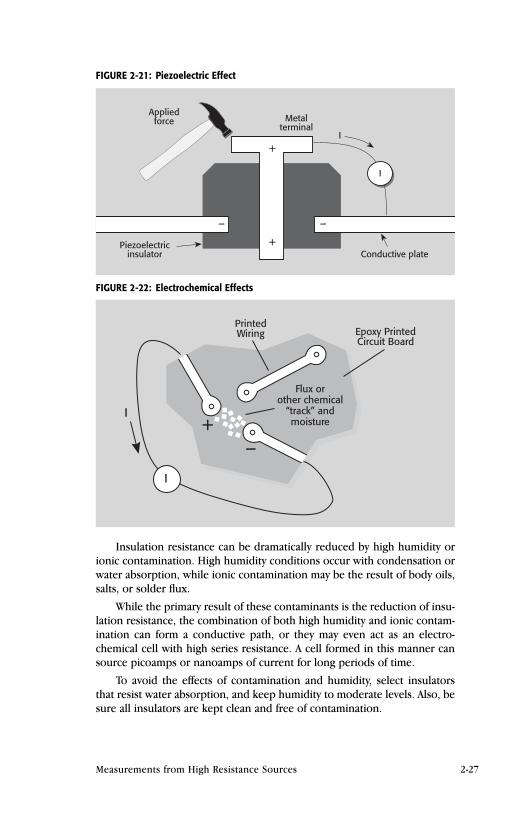
FIGURE 2-22: Electrochemical Effects
Insulation resistance can be dramatically reduced by high humidity orionic contamination. High humidity conditions occur with condensation orwater absorption, while ionic contamination may be the result of body oils,salts, or solder flux.
While the primary result of these contaminants is the reduction of insu-lation resistance, the combination of both high humidity and ionic contam-ination can form a conductive path, or they may even act as an electro-chemical cell with high series resistance. A cell formed in this manner cansource picoamps or nanoamps of current for long periods of time.
To avoid the effects of contamination and humidity, select insulatorsthat resist water absorption, and keep humidity to moderate levels. Also, besure all insulators are kept clean and free of contamination.
I
PrintedWiring Epoxy Printed
Circuit Board
Flux orother chemical
“track” andmoisture+
–
I
Measurements from High Resistance Sources 2-27
FIGURE 2-21: Piezoelectric Effect
I
Metalterminal
+
+
Appliedforce
– –
Piezoelectricinsulator Conductive plate
I

If insulators become contaminated, apply a cleaning agent such asmethanol to all interconnecting circuitry. It’s important to flush away allcontaminants once they’re dissolved in the solvent, so they won’t be rede-posited. Use only very pure solvents for cleaning; lower grades may containcontaminants that leave an electrochemical film.
Dielectric Absorption
Dielectric absorption in an insulator can occur when a voltage across thatinsulator causes positive and negative charges within the insulator to polar-ize because various polar molecules relax at different rates. When the volt-age is removed, the separated charges generate a decaying current throughcircuits connected to the insulator as they recombine.
To minimize the effects of dielectric absorption on current measure-ments, avoid applying voltages greater than a few volts to insulators beingused for sensitive current measurements. In cases where this practice isunavoidable, it may take minutes or even hours in some cases for the cur-rent caused by dielectric absorption to dissipate.
Table 2-2 in Section 2.2.2 summarizes the relative dielectric absorptionof various insulating materials.
2.3.5 Voltage Burden
An ammeter may be represented by an ideal ammeter (IM) with zero inter-nal resistance, in series with a resistance (RM), as shown in Figure 2-23.When a current source whose Thevenin equivalent circuit is a voltage (VS)in series with a source resistance (RS) is connected to the input of theammeter, the current is reduced from what it would be with the idealammeter (RM = 0Ω). This reduction is caused by the internal resistance(RM), which creates an additional voltage drop called the voltage burden(VB).
The voltage burden is specified for a full-scale input. Therefore, thevoltage burden at a given current can be calculated by:
where IFS is full scale current and IS is the magnitude of the current source.
Taking into account the voltage burden, the measurement error can becalculated as follows:
IM =VS – VB
RS
IS
IFS
VBIS
IFSVB(I) =
2-28 SECTION 2
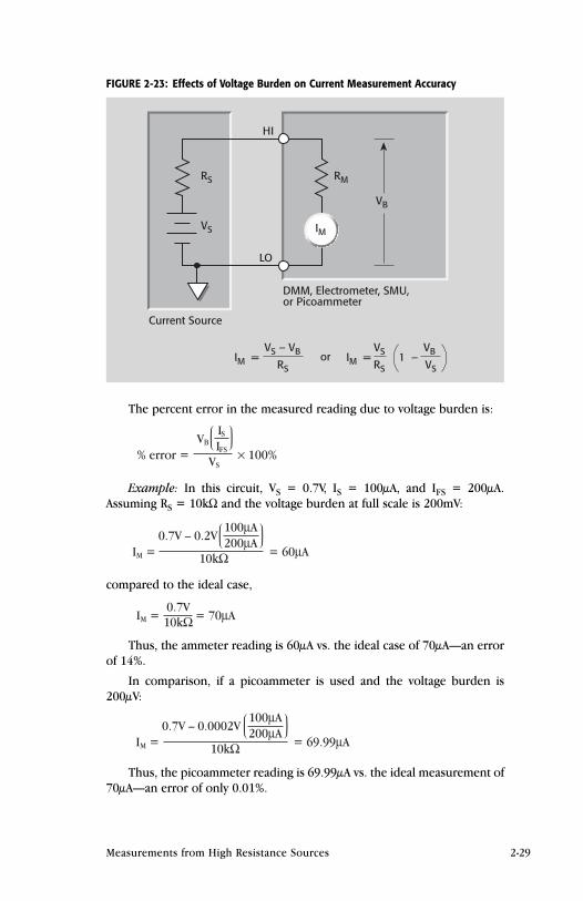
The percent error in the measured reading due to voltage burden is:
Example: In this circuit, VS = 0.7V, IS = 100µA, and IFS = 200µA.Assuming RS = 10kΩ and the voltage burden at full scale is 200mV:
compared to the ideal case,
Thus, the ammeter reading is 60µA vs. the ideal case of 70µA—an errorof 14%.
In comparison, if a picoammeter is used and the voltage burden is200µV:
Thus, the picoammeter reading is 69.99µA vs. the ideal measurement of70µA—an error of only 0.01%.
IM =0.7V – 0.0002V
10kΩ
100µA200µA
= 69.99µA
IM =0.7V10kΩ = 70µA
IM =0.7V – 0.2V
10kΩ
100µA200µA
= 60µA
% error =VB
VS
ISIFS × 100%
Measurements from High Resistance Sources 2-29
FIGURE 2-23: Effects of Voltage Burden on Current Measurement Accuracy
VS
RS RM
IM
HI
LO
DMM, Electrometer, SMU,or Picoammeter
VB
Current Source
IM =RS
VS
VS
VB1 –IM =RS
VS – VB or
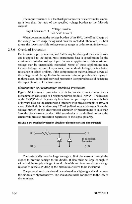
The input resistance of a feedback picoammeter or electrometer amme-ter is less than the ratio of the specified voltage burden to the full-scalecurrent:
Voltage BurdenInput Resistance < _____________________
Full Scale Current
When determining the voltage burden of an SMU, the offset voltage onthe voltage source range being used must be included. Therefore, it’s bestto use the lowest possible voltage source range in order to minimize error.
2.3.6 Overload ProtectionElectrometers, picoammeters, and SMUs may be damaged if excessive volt-age is applied to the input. Most instruments have a specification for themaximum allowable voltage input. In some applications, this maximumvoltage may be unavoidably exceeded. Some of these applications mayinclude leakage current of capacitors, reverse diode leakage, or insulationresistance of cables or films. If the component or material breaks down, allthe voltage would be applied to the ammeter’s input, possibly destroying it.In these cases, additional overload protection is required to avoid damagingthe input circuitry of the instrument.
Electrometer or Picoammeter Overload Protection
Figure 2-24 shows a protection circuit for an electrometer ammeter orpicoammeter, consisting of a resistor and two diodes (1N3595). The leakageof the 1N3595 diode is generally less than one picoampere even with 1mVof forward bias, so the circuit won’t interfere with measurements of 10pA ormore. This diode is rated to carry 225mA (450mA repeated surge). Since thevoltage burden of the electrometer ammeter or picoammeter is less than1mV, the diodes won’t conduct. With two diodes in parallel back to back, thecircuit will provide protection regardless of the signal polarity.
FIGURE 2-24: Overload Protection Circuit for Electrometers and Picoammeters
The resistor (R) must be large enough to limit the current through thediodes to prevent damage to the diodes. It also must be large enough towithstand the supply voltage. A good rule of thumb is to use a large enoughresistor to cause a 1V drop at the maximum current to be measured.
The protection circuit should be enclosed in a light-tight shield becausethe diodes are photosensitive. The shield should be connected to the low ofthe ammeter.
R
To FeedbackAmmeter
HI
LO
HI
LO
2-30 SECTION 2
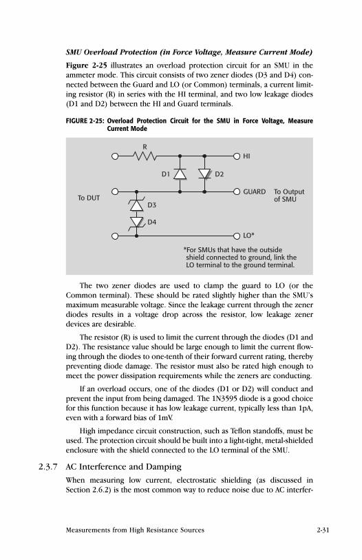
SMU Overload Protection (in Force Voltage, Measure Current Mode)
Figure 2-25 illustrates an overload protection circuit for an SMU in theammeter mode. This circuit consists of two zener diodes (D3 and D4) con-nected between the Guard and LO (or Common) terminals, a current limit-ing resistor (R) in series with the HI terminal, and two low leakage diodes(D1 and D2) between the HI and Guard terminals.
FIGURE 2-25: Overload Protection Circuit for the SMU in Force Voltage, MeasureCurrent Mode
The two zener diodes are used to clamp the guard to LO (or the Common terminal). These should be rated slightly higher than the SMU’smaximum measurable voltage. Since the leakage current through the zenerdiodes results in a voltage drop across the resistor, low leakage zenerdevices are desirable.
The resistor (R) is used to limit the current through the diodes (D1 andD2). The resistance value should be large enough to limit the current flow-ing through the diodes to one-tenth of their forward current rating, therebypreventing diode damage. The resistor must also be rated high enough tomeet the power dissipation requirements while the zeners are conducting.
If an overload occurs, one of the diodes (D1 or D2) will conduct andprevent the input from being damaged. The 1N3595 diode is a good choicefor this function because it has low leakage current, typically less than 1pA,even with a forward bias of 1mV.
High impedance circuit construction, such as Teflon standoffs, must beused. The protection circuit should be built into a light-tight, metal-shieldedenclosure with the shield connected to the LO terminal of the SMU.
2.3.7 AC Interference and DampingWhen measuring low current, electrostatic shielding (as discussed inSection 2.6.2) is the most common way to reduce noise due to AC interfer-
R
To Outputof SMU
HI
GUARDTo DUT
LO*
D2D1
D3
D4
*For SMUs that have the outsideshield connected to ground, link theLO terminal to the ground terminal.
Measurements from High Resistance Sources 2-31
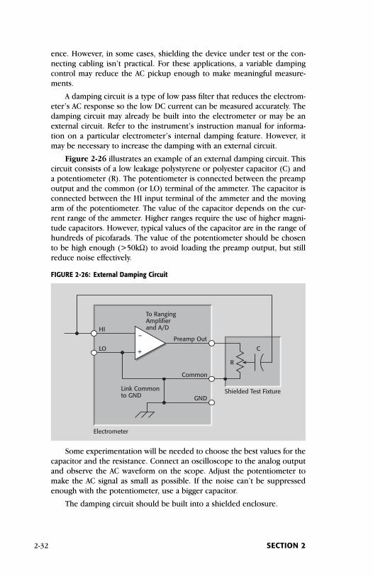
ence. However, in some cases, shielding the device under test or the con-necting cabling isn’t practical. For these applications, a variable dampingcontrol may reduce the AC pickup enough to make meaningful measure-ments.
A damping circuit is a type of low pass filter that reduces the electrom-eter’s AC response so the low DC current can be measured accurately. Thedamping circuit may already be built into the electrometer or may be anexternal circuit. Refer to the instrument’s instruction manual for informa-tion on a particular electrometer’s internal damping feature. However, itmay be necessary to increase the damping with an external circuit.
Figure 2-26 illustrates an example of an external damping circuit. Thiscircuit consists of a low leakage polystyrene or polyester capacitor (C) anda potentiometer (R). The potentiometer is connected between the preampoutput and the common (or LO) terminal of the ammeter. The capacitor isconnected between the HI input terminal of the ammeter and the movingarm of the potentiometer. The value of the capacitor depends on the cur-rent range of the ammeter. Higher ranges require the use of higher magni-tude capacitors. However, typical values of the capacitor are in the range ofhundreds of picofarads. The value of the potentiometer should be chosento be high enough (>50kΩ) to avoid loading the preamp output, but stillreduce noise effectively.
FIGURE 2-26: External Damping Circuit
Some experimentation will be needed to choose the best values for thecapacitor and the resistance. Connect an oscilloscope to the analog outputand observe the AC waveform on the scope. Adjust the potentiometer tomake the AC signal as small as possible. If the noise can’t be suppressedenough with the potentiometer, use a bigger capacitor.
The damping circuit should be built into a shielded enclosure.
–
+
R
HI
LO
To RangingAmplifierand A/D
Preamp Out
Common
GND
Link Commonto GND
C
Electrometer
Shielded Test Fixture
2-32 SECTION 2
2.3.8 Using a Coulombmeter to Measure Low CurrentIn most cases, an ammeter or picoammeter is used to measure current.However, for femtoamp-level currents, it may be better to use the coulombsfunction of an electrometer to measure the change in charge over time, thenuse those charge measurements to determine the current. A further discus-sion of charge measurements can be found in Section 2.5.
Basic Charge Measurement Methods
Charge is difficult to measure directly; it must be related to an easily meas-ured quantity. One commonly used method of making this type of meas-urement is to measure the voltage across a capacitor of known value. Thecharge is related to capacitor voltage as follows:
Q = CV
where: Q = capacitor charge (coulombs)C = capacitor value (farads)V = voltage across capacitor (volts)
Once the rate of change in charge is known, the current can easily bedetermined from the charge measurement. The instantaneous current (i) issimply:
dQi = ____
dt
while the long-term average current is defined as:
∆QIAVG = ____
∆t
Thus, we see that charge can be measured and current can be deter-mined simply by making a series of voltage measurements.
Using a Feedback Coulombmeter to Measure Current
Charge can be measured directly with a feedback coulombmeter. Figure 2-27 shows a simplified model of a feedback type coulombmeter. The inputcurrent to the circuit is IS, the output voltage is VOUT, and the feedbackcapacitor is CF.
The current (IS) is applied to the input of the feedback coulombmeter.The circuit is an integrator, so the charge is determined by integrating thecurrent:
QM = ∫ i dt
The coulombmeter determines charge from the output voltage and thevalue of the feedback capacitor:
QM = CFVOUT
From the measured charge (QM), the user can calculate current:
Measurements from High Resistance Sources 2-33
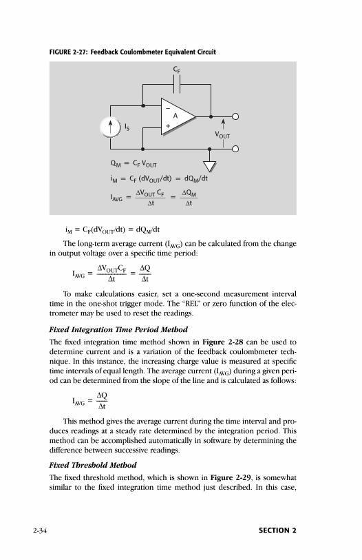
iM = CF(dVOUT/dt) = dQM/dt
The long-term average current (IAVG) can be calculated from the changein output voltage over a specific time period:
∆VOUTCF ∆QIAVG = __________ = ____
∆t ∆t
To make calculations easier, set a one-second measurement intervaltime in the one-shot trigger mode. The “REL” or zero function of the elec-trometer may be used to reset the readings.
Fixed Integration Time Period Method
The fixed integration time method shown in Figure 2-28 can be used todetermine current and is a variation of the feedback coulombmeter tech-nique. In this instance, the increasing charge value is measured at specifictime intervals of equal length. The average current (IAVG) during a given peri-od can be determined from the slope of the line and is calculated as follows:
∆QIAVG = ____
∆t
This method gives the average current during the time interval and pro-duces readings at a steady rate determined by the integration period. Thismethod can be accomplished automatically in software by determining thedifference between successive readings.
Fixed Threshold Method
The fixed threshold method, which is shown in Figure 2-29, is somewhatsimilar to the fixed integration time method just described. In this case,
2-34 SECTION 2
FIGURE 2-27: Feedback Coulombmeter Equivalent Circuit
QM = CF VOUT
iM = CF (dVOUT/dt) = dQM/dt
∆VOUT CF
∆tIAVG = =
∆QM
∆t
–
+IS
CF
VOUT
A

however, the charge measurement begins at time t1 and continues until thecharge value reaches some predetermined threshold value at time t2. Thecurrent is then calculated as follows:
∆QIAVG = ____ where ∆t = t2 – t1∆t
Note that the voltage coefficient of the coulombmeter capacitor has lit-tle effect on overall current measurement accuracy. As long as the thresholdpoint and time periods are accurately known, current measurement accura-cy will be quite good. However, readings won’t be evenly spaced when cur-rent levels vary, and the interval between readings can be quite long whenthe average current for a given time period is small.
Measurements from High Resistance Sources 2-35
∆Q
∆t
∆Q∆tIAVG =
Q
tFixed time intervals
FIGURE 2-28: Fixed Integration Time Method of Determining Current from Charge
FIGURE 2-29: Fixed Threshold Method of Determining Current from Charge
∆Q
∆t
Q
tt1 t2
Fixed threshold
∆Q∆tIAVG =
Advantages of Using a Coulombmeter to Measure Current
There are several advantages to using a coulombmeter instead of an amme-ter for measuring current in certain situations:
• Lower Current Noise: The ammeter uses a feedback resistor, whichwill have significant Johnson noise. For charge measurement, thisresistor is replaced by a capacitor, which theoretically has noJohnson noise. Consequently, the charge method of current mea-surement results in lower noise than measuring currents directlywith a feedback ammeter. Thus, the charge method is preferablewhen current noise performance less than 1fA p-p is required. (Referto Figure 2-52 in Section 2.6.5 and note that feedback resistanceshigher than 1012Ω aren’t very practical.)
• Faster Settling Times: The speed of a feedback ammeter is limitedby the time constant of its feedback circuit (RFCF). For example, forfeedback resistances greater than 10GΩ, stray capacitance limitsresponse times to tens of milliseconds. In contrast, a feedback inte-grator will respond immediately and is limited only by the speed ofthe operational amplifier.
• Random Pulses Can Be Integrated: The average charge transferredper unit time of random pulse trains can be evaluated by integratingthe current pulse train for a given period of time. The average cur-rent amplitudes can then be expressed as the total charge divided bythe time period involved in the measurement. This technique isespecially useful when averaging very small, unsteady currents. If theduty cycle is known, the pulse height can also be determined.
• The Noise Effects of Input Shunt Capacitance are Minimized:Noise gain is mainly determined by CIN/CF, and CF is much larger ina coulombmeter than in an ammeter, so much larger input capaci-tance values can be tolerated. This characteristic is beneficial whenmeasuring from high capacitance sources or when long connectingcables are used.
2.4 High Resistance MeasurementsWhen resistances greater than 1GΩ must be measured, an electrometer,SMU, or picoammeter/voltage source are usually required. An electrometermay measure high resistance by either the constant-voltage or the constant-current method. Some electrometers allow the user to choose eithermethod. The constant-voltage method uses an ammeter and a voltagesource, while the constant-current method uses an electrometer voltmeterand a current source. A description of these techniques follows.
2.4.1 Constant-Voltage Method
To make high resistance measurements using the constant-voltage method,an instrument that can measure low current and a constant DC voltage
2-36 SECTION 2
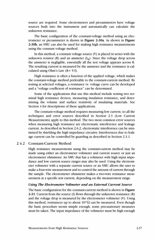
Measurements from High Resistance Sources 2-37
source are required. Some electrometers and picoammeters have voltagesources built into the instrument and automatically can calculate theunknown resistance.
The basic configuration of the constant-voltage method using an elec-trometer or picoammeter is shown in Figure 2-30a. As shown in Figure 2-30b, an SMU can also be used for making high resistance measurementsusing the constant voltage method.
In this method, a constant voltage source (V) is placed in series with theunknown resistor (R) and an ammeter (IM). Since the voltage drop acrossthe ammeter is negligible, essentially all the test voltage appears across R.The resulting current is measured by the ammeter and the resistance is cal-culated using Ohm’s Law (R= V/I).
High resistance is often a function of the applied voltage, which makesthe constant-voltage method preferable to the constant-current method. Bytesting at selected voltages, a resistance vs. voltage curve can be developedand a “voltage coefficient of resistance” can be determined.
Some of the applications that use this method include testing two ter-minal high resistance devices, measuring insulation resistance, and deter-mining the volume and surface resistivity of insulating materials. SeeSection 4 for descriptions of these applications.
The constant-voltage method requires measuring low current, so all thetechniques and error sources described in Section 2.3 (Low CurrentMeasurements) apply to this method. The two most common error sourceswhen measuring high resistance are electrostatic interference and leakagecurrent. As described in Section 2.6.2, electrostatic interference can be min-imized by shielding the high impedance circuitry. Interferences due to leak-age current can be controlled by guarding as described in Section 2.3.1.
2.4.2 Constant-Current MethodHigh resistance measurements using the constant-current method may bemade using either an electrometer voltmeter and current source or just anelectrometer ohmmeter. An SMU that has a voltmeter with high input impe-dance and low current source ranges may also be used. Using the electrom-eter voltmeter with a separate current source or an SMU allows the user tomake a four-wire measurement and to control the amount of current throughthe sample. The electrometer ohmmeter makes a two-wire resistance meas-urement at a specific test current, depending on the measurement range.
Using The Electrometer Voltmeter and an External Current Source
The basic configuration for the constant-current method is shown in Figure2-31. Current from the source (I) flows through the unknown resistance (R)and the voltage drop is measured by the electrometer voltmeter (V). Usingthis method, resistances up to about 1012Ω can be measured. Even thoughthe basic procedure seems simple enough, some precautionary measuresmust be taken. The input impedance of the voltmeter must be high enough
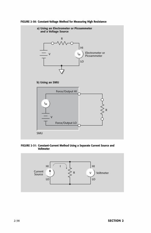
2-38 SECTION 2
FIGURE 2-30: Constant-Voltage Method for Measuring High Resistance
V
SMU
b) Using an SMU
Force/Output HI
Force/Output LO
IM
R
V
a) Using an Electrometer or Picoammeterand a Voltage Source
IM
R
Electrometer orPicoammeter
HI
LO
RCurrentSource VoltmeterV
HI
LO
HI
LO
I
FIGURE 2-31: Constant-Current Method Using a Separate Current Source andVoltmeter
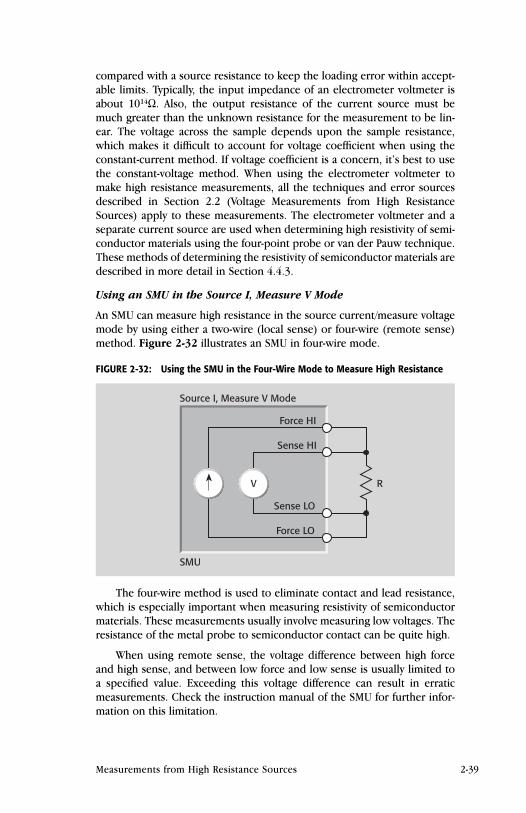
compared with a source resistance to keep the loading error within accept-able limits. Typically, the input impedance of an electrometer voltmeter isabout 1014Ω. Also, the output resistance of the current source must bemuch greater than the unknown resistance for the measurement to be lin-ear. The voltage across the sample depends upon the sample resistance,which makes it difficult to account for voltage coefficient when using theconstant-current method. If voltage coefficient is a concern, it’s best to usethe constant-voltage method. When using the electrometer voltmeter tomake high resistance measurements, all the techniques and error sourcesdescribed in Section 2.2 (Voltage Measurements from High ResistanceSources) apply to these measurements. The electrometer voltmeter and aseparate current source are used when determining high resistivity of semi-conductor materials using the four-point probe or van der Pauw technique.These methods of determining the resistivity of semiconductor materials aredescribed in more detail in Section 4.4.3.
Using an SMU in the Source I, Measure V Mode
An SMU can measure high resistance in the source current/measure voltagemode by using either a two-wire (local sense) or four-wire (remote sense)method. Figure 2-32 illustrates an SMU in four-wire mode.
FIGURE 2-32: Using the SMU in the Four-Wire Mode to Measure High Resistance
The four-wire method is used to eliminate contact and lead resistance,which is especially important when measuring resistivity of semiconductormaterials. These measurements usually involve measuring low voltages. Theresistance of the metal probe to semiconductor contact can be quite high.
When using remote sense, the voltage difference between high forceand high sense, and between low force and low sense is usually limited toa specified value. Exceeding this voltage difference can result in erraticmeasurements. Check the instruction manual of the SMU for further infor-mation on this limitation.
V R
Force HI
Sense HI
Sense LO
Force LO
SMU
Source I, Measure V Mode
Measurements from High Resistance Sources 2-39
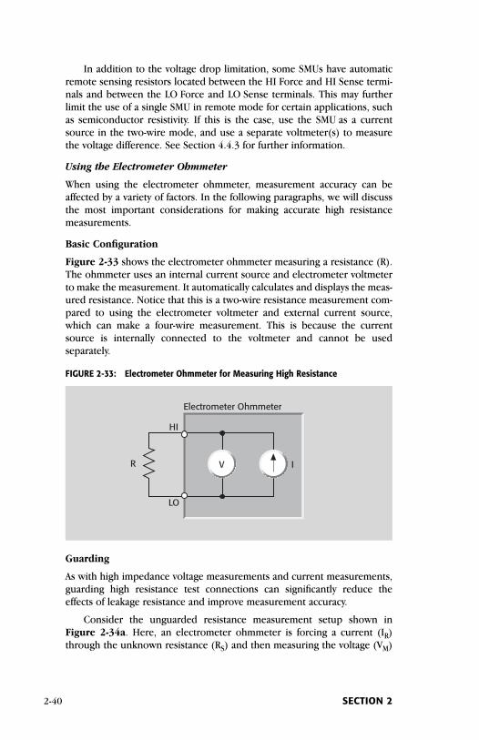
In addition to the voltage drop limitation, some SMUs have automaticremote sensing resistors located between the HI Force and HI Sense termi-nals and between the LO Force and LO Sense terminals. This may furtherlimit the use of a single SMU in remote mode for certain applications, suchas semiconductor resistivity. If this is the case, use the SMU as a currentsource in the two-wire mode, and use a separate voltmeter(s) to measurethe voltage difference. See Section 4.4.3 for further information.
Using the Electrometer Ohmmeter
When using the electrometer ohmmeter, measurement accuracy can beaffected by a variety of factors. In the following paragraphs, we will discussthe most important considerations for making accurate high resistancemeasurements.
Basic Configuration
Figure 2-33 shows the electrometer ohmmeter measuring a resistance (R).The ohmmeter uses an internal current source and electrometer voltmeterto make the measurement. It automatically calculates and displays the meas-ured resistance. Notice that this is a two-wire resistance measurement com-pared to using the electrometer voltmeter and external current source,which can make a four-wire measurement. This is because the currentsource is internally connected to the voltmeter and cannot be usedseparately.
FIGURE 2-33: Electrometer Ohmmeter for Measuring High Resistance
Guarding
As with high impedance voltage measurements and current measurements,guarding high resistance test connections can significantly reduce theeffects of leakage resistance and improve measurement accuracy.
Consider the unguarded resistance measurement setup shown inFigure 2-34a. Here, an electrometer ohmmeter is forcing a current (IR)through the unknown resistance (RS) and then measuring the voltage (VM)
R
HI
Electrometer Ohmmeter
V
LO
I
2-40 SECTION 2
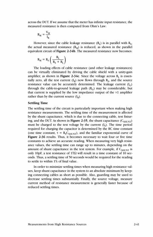
across the DUT. If we assume that the meter has infinite input resistance, themeasured resistance is then computed from Ohm’s Law:
VMRM = ____IR
However, since the cable leakage resistance (RL) is in parallel with RS,the actual measured resistance (RM) is reduced, as shown in the parallelequivalent circuit of Figure 2-34b. The measured resistance now becomes:
RLRM = RS____________( RS + RL
)The loading effects of cable resistance (and other leakage resistances)
can be virtually eliminated by driving the cable shield with a unity-gainamplifier, as shown in Figure 2-34c. Since the voltage across RL is essen-tially zero, all the test current (IR) now flows through RS, and the sourceresistance value can be accurately determined. The leakage current (IG)through the cable-to-ground leakage path (RG) may be considerable, butthat current is supplied by the low impedance output of the ×1 amplifierrather than by the current source (IR).
Settling Time
The settling time of the circuit is particularly important when making highresistance measurements. The settling time of the measurement is affectedby the shunt capacitance, which is due to the connecting cable, test fixtur-ing, and the DUT. As shown in Figure 2-35, the shunt capacitance (CSHUNT)must be charged to the test voltage by the current (IS). The time periodrequired for charging the capacitor is determined by the RC time constant(one time constant, τ = RSCSHUNT), and the familiar exponential curve ofFigure 2-36 results. Thus, it becomes necessary to wait four or five timeconstants to achieve an accurate reading. When measuring very high resist-ance values, the settling time can range up to minutes, depending on theamount of shunt capacitance in the test system. For example, if CSHUNT isonly 10pF, a test resistance of 1TΩ will result in a time constant of 10 sec-onds. Thus, a settling time of 50 seconds would be required for the readingto settle to within 1% of final value.
In order to minimize settling times when measuring high resistance val-ues, keep shunt capacitance in the system to an absolute minimum by keep-ing connecting cables as short as possible. Also, guarding may be used todecrease settling times substantially. Finally, the source voltage, measurecurrent method of resistance measurement is generally faster because ofreduced settling times.
Measurements from High Resistance Sources 2-41
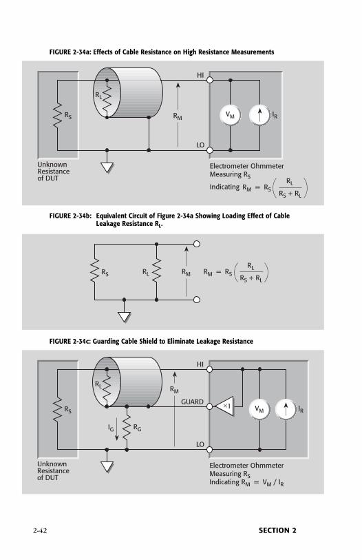
2-42 SECTION 2
FIGURE 2-34a: Effects of Cable Resistance on High Resistance Measurements
RS
Electrometer OhmmeterMeasuring RS
Indicating
UnknownResistanceof DUT
RM
HI
LO
RL
VM IR
RM = RSRS + RL
RL
FIGURE 2-34b: Equivalent Circuit of Figure 2-34a Showing Loading Effect of CableLeakage Resistance RL.
RS RMRL RM = RSRS + RL
RL
FIGURE 2-34c: Guarding Cable Shield to Eliminate Leakage Resistance
IG
RS
Electrometer OhmmeterMeasuring RSIndicating RM = VM / IR
UnknownResistanceof DUT
RM
HI
LO
RG
GUARD ×1
RL
VM IR
2.4.3 Characteristics of High Ohmic Valued ResistorsResistors with values of 1GΩ or more are often referred to as high megohmresistors. Their high resistances make these components very unusualdevices, so take several considerations into account when measuring them:voltage and temperature coefficients, the effects of mechanical shock, andcontamination.
Two types of high megohm resistors are widely used: carbon-film andmetal-oxide. When compared with conventional resistors, carbon-film highmegohm resistors are noisy, unstable, have high temperature coefficients,display high voltage coefficients, and are very fragile. Recent developmentsin metal-oxide types have resulted in resistors with much lower voltagecoefficients, as well as improved temperature and time stability. Moderndevices exhibit voltage coefficients less than 5ppm/V and no significant driftafter five years of tests. Temperature coefficients are on the order of0.01%/°C at 100MΩ, 0.025%/°C at 100GΩ.
Measurements from High Resistance Sources 2-43
Time
99
0 1.0 2.0 3.0 4.0 5.0
63Percentof FinalValue
0
τ = RS CSHUNT
FIGURE 2-35: Settling Time is the Result of RSCSHUNT Time Constant
UnknownResistanceof DUT
RS CSHUNTVM
Ohmmeter
τ = RS CSHUNT
IS
FIGURE 2-36: Exponential Settling Time Caused by Time Constant of ShuntCapacitance and Source Resistance
Such devices require extreme care in handling. Mechanical shock maysignificantly alter the resistance by dislodging particles of the conductivematerial. It’s also important not to touch the resistance element or the glassenvelope that surrounds it; doing so could change its resistance due to thecreation of new current paths or small electrochemically generated currents.
The resistors are coated to prevent water films from forming on the sur-face. Therefore, if a resistor acquires surface films from careless handling ordeposits from air contaminants, it should be cleaned with a foam-tipped swaband methanol. After cleaning, the resistor should be dried in a low humidityatmosphere for several hours to allow any static charges to dissipate.
2.5 Charge MeasurementsCharge is the time integral of current, q = ∫ idt. Charge is often measuredon a quantity of particles, on a surface, or on a component such as a capac-itor. Sometimes, the charge is measured on a continuous basis, such aswhen using the coulombmeter to measure very low current, as discussed inSection 2.3.8.
An electrometer makes an ideal coulombmeter because it has very lowinput offset current and high input resistance. The coulombmeter functionof the electrometer measures charge by integrating the input current. Anintegrating capacitor is used in the feedback loop of the input stage. Referto Section 1.5.3 for a more detailed discussion of the coulombmeter circuitof the electrometer.
2.5.1 Error SourcesCharge measurements made with an electrometer are subject to a numberof error sources, including input offset current, voltage burden, generatedcurrents, and low source impedance.
Input Offset Current
With an electrometer, the input offset current is very low. However, at lowcharge levels, even this small current may be a significant error factor. Overlong time periods, the instrument will integrate the offset current, whichwill be seen as a long-term drift in the charge measurement. Typical offsetcurrent is 4fA, which will cause a change in the charge measurement of 4fCper second. If the offset current is known, it’s possible to compensate forthis error simply by subtracting the charge drift due to offset current fromthe actual reading. However, determining the offset current of the entiresystem may be difficult.
Voltage Burden
The voltage burden of a feedback coulombmeter is generally quite low(<100µV), just as it is with a feedback picoammeter. However, if the instan-taneous peak current is >10µA, the voltage burden can exceed this levelmomentarily. In an overload condition, the voltage burden can reach manyvolts, depending on the input value.
2-44 SECTION 2
If the source voltage is at least 10mV, the typical electrometer in thecoulombs mode will integrate the current accurately. If the source voltage ismuch lower, the voltage burden may become a problem, and the input stagenoise will be amplified so much that accurate measurements aren’t possible.
Generated Currents
Generated currents from the input cable or induced currents due to insuf-ficient shielding can cause errors in charge measurements, especially withcharge levels of 100pC or less. To minimize generated currents, use lownoise cable and electrostatically shield all connections and the DUT.
Source Impedance
The magnitude of the source impedance can affect the noise performanceof the feedback coulombmeter. Figure 2-37 shows a generalized feedbackcircuit connected to a source impedance. In a coulombmeter, the feedbackimpedance is a capacitor. From this diagram, the noise gain of the coulomb-meter can be calculated from the following equation:
Output Noise = Input Noise × (1 + ZF/ZS)
where:ZS is the source impedanceZF is the feedback impedance of the coulombmeterInput Noise is the noise of the input stage of the electrometer
FIGURE 2-37: Generalized Feedback Circuit
In general, as ZF becomes larger, the noise gain becomes larger. Referto the electrometer’s manual or specifications for the value of the feedbackimpedance for a particular instrument.
2.5.2 Zero CheckUnlike a voltage measurement, a charge measurement can be a destructivemeasurement. In other words, the process of making the measurement mayremove the charge stored in the device under test.
When measuring the charge on a device such as a capacitor, it’s impor-tant to disable the zero check of the electrometer first, and then connect thecapacitor to the high impedance input terminal. Otherwise, some of the
–
+ZS
ZF
OutputNoise
InputNoise
Measurements from High Resistance Sources 2-45
charge will be lost through the zero check impedance and won’t be meas-ured by the electrometer. That’s because when zero check is enabled, theinput resistance of the electrometer is about 10MΩ.
Opening the zero check switch will produce a sudden change in chargereading known as “zero hop.” To eliminate the effects of zero hop, take areading just after the zero check is disabled, then subtract this value from allsubsequent readings. An easy way to do this is to enable the REL functionafter zero check is disabled, which nulls out the charge reading caused by the hop.
2.5.3 Extending the Charge Measurement Range of the ElectrometerThe charge measurement range of most electrometers can be extendedusing external feedback. The external feedback mode allows an externaldevice to be used as the feedback element of the electrometer. Placing theelectrometer in the volts mode and then enabling external feedback switch-es the feedback circuit from an internal network to a feedback circuit con-nected to the preamp output.
To extend the coulombs ranges, an external capacitor is used as thefeedback element.
As illustrated in Figure 2-38, an external feedback capacitor is placedbetween the preamp output terminal and the HI input terminal of the elec-trometer. To prevent electrostatic interference, the capacitor is placed in ashielded test fixture.
FIGURE 2-38: Connections for Using External Feedback Capacitor
When in the external feedback mode, the electrometer will display thevoltage across the feedback element. The unknown charge can be calculat-ed from the following formula:
Q = CV
2-46 SECTION 2
To RangingAmplifierand A/D
–
+
HI
LO
GND
Preamp Out
Electrometer
Q
UnknownChargeto be
Determined
ExternalFeedbackCapacitor
Shielded Test Fixture
where: Q = charge (coulombs)C = capacitance of the external feedback capacitor (farads)V = voltage on display of electrometer (volts)
For example, using an external feedback capacitor of 10µF and meas-uring 5V on the display of the electrometer, the calculated charge is 50µC.
The capacitance of the feedback element should be at least 10pF toavoid errors due to stray capacitance and noise gain.
To ensure low leakage current and low dielectric absorption, the feed-back capacitor should be made of a suitable dielectric material such as poly-styrene, polypropylene, or Teflon.
More information on the measurement procedure can be found in theinstruction manual of the electrometer.
2.6 General Electrometer ConsiderationsSo far, we have discussed considerations specific to voltage, current, resist-ance, and charge measurements. The following paragraphs examine con-siderations that apply to all types of electrometer and SMU measurementson high resistance sources.
2.6.1 Making ConnectionsTo avoid measurement errors, it’s critical to make proper connections fromthe electrometer, SMU, or picoammeter to the device under test. Alwaysconnect the high resistance terminal of the meter to the highest resist-ance point of the circuit under test.
Figure 2-39 shows an electrometer connected to a current source thatconsists of a voltage source in series with a resistor. An AC powered sourceusually has a significant level (often several volts) of line frequency commonmode voltage. As shown in Figure 2-40, this will cause a current (i) to flowthrough the low to ground capacitance of the electrometer (IM). This circuit
Measurements from High Resistance Sources 2-47
FIGURE 2-39: Connecting the HI Terminal of the Ammeter to High Resistance
R
Current Source
HI
LO
IM
is connected properly, so this current doesn’t flow through the electrome-ter measurement circuitry and, therefore, doesn’t cause any measurementerrors. However, when the HI terminal of the electrometer is connected tothe low impedance power supply, this AC current (i) flows through the elec-trometer (IM), as illustrated in Figure 2-41. This current may affect themeasurement accuracy, especially at low signal levels.
2-48 SECTION 2
FIGURE 2-40: Proper Connection
R
Current Source
HI
LO
IM
i
FIGURE 2-41: Improper Connection
R
Current Source
LO
HI
IM
i

See Section 2.6.6 for details on appropriate cabling and connector typesfor electrometer measurements.
2.6.2 Electrostatic Interference and ShieldingElectrostatic coupling or interference occurs when an electrically chargedobject approaches the input circuit under test. At low impedance levels, theeffects of the interference aren’t noticeable because the charge dissipatesrapidly. However, high resistance materials don’t allow the charge to decayquickly, which may result in unstable measurements. The erroneous read-ings may be due to either DC or AC electrostatic fields, so electrostaticshielding will help minimize the effects of these fields.
DC fields can produce noisy readings or undetected errors. These fieldscan be detected when movement near an experiment (such as the move-ment of the person operating the instrument or others in the immediatevicinity) causes fluctuations on the electrometer’s display. To perform aquick check for interference, place a piece of charged plastic, such as acomb, near the circuit. A large change in the meter reading indicates insuf-ficient shielding.
AC fields can be equally troublesome. These are caused most often bypower lines and RF fields. If the AC voltage at the input is large, part of thissignal is rectified, producing an error in the DC signal being measured. Thiscan be checked by observing the analog output of the electrometer orpicoammeter with an oscilloscope. A clipped waveform indicates a need toimprove electrostatic shielding. Figure 2-42 illustrates a clipped waveformtaken from the 2V analog output of an electrometer. In this example, theamount of clipping reduced the DC current reading by nearly 50%.
FIGURE 2-42: Clipped Waveform from the Analog Output of an Electrometer Caused by AC Pickup
For an SMU, check for AC pickup by connecting the oscilloscopebetween the guard terminal and common.
Measurements from High Resistance Sources 2-49
Figure 2-43 shows an example of AC electrostatic coupling. An elec-trostatic voltage source in the vicinity of a conductor, such as a cable or traceon a PC board, generates a current proportional to the rate of change of thevoltage and of the coupling capacitance. This current can be calculated withthe following equation:
i = C dV/dt + V dC/dt
For example, two conductors, each with 1cm2 area and spaced 1cmapart by air, will have almost 0.1pF of capacitance. With a voltage differenceof 100V between the two conductors and a vibration causing a change ofcapacitance of 0.01pF/second (a 10% fluctuation between them), a currentof 1pA AC will be generated.
To reduce the effects of the fields, a shield can be built to enclose thecircuit being measured. The easiest type of shield to make is a simple metalbox or meshed screen that encloses the test circuit. Shielded boxes are alsoavailable commercially.
FIGURE 2-43: Electrostatic Coupling
Figure 2-44 illustrates an example of shielding. Made from a conduc-tive material, the shield is always connected to the low impedance input ofthe electrometer or picoammeter or to the output LO (or common) termi-nal of the SMU. If circuit LO is floating above ground, observe special safe-ty precautions to prevent anyone from touching the shield. These safety pre-cautions are discussed in Section 2.6.8.
The cabling between the HI terminal of the meter and the device undertest also requires shielding. Capacitive coupling between an electrostaticnoise source and the signal conductors or cables can be greatly reduced bysurrounding those conductors with a metal shield connected to LO, asshown in Figure 2-45. With this shield in place, the noise current generat-ed by the electrostatic voltage source and the coupling capacitance flowsthrough the shield to ground rather than through the signal conductors.
V
C
Electrostaticvoltage source
GroundReferencedSignalConductor
i
Couplingcapacitance
i = C + VdVdt
dCdt
2-50 SECTION 2
FIGURE 2-45: Electrostatic Shielding
To summarize, follow these guidelines to minimize error currents dueto electrostatic coupling:
• Keep all charged objects (including people) and conductors awayfrom sensitive areas of the test circuit.
• Avoid movement and vibration near the test area.
• When measuring currents <1nA, shield the device under test by sur-rounding it with a metal enclosure and connect the enclosure elec-trically to the test circuit common terminal.
Shielding vs. Guarding
Shielding usually implies the use of a metallic enclosure to prevent electro-static interference from affecting a high impedance circuit. Guardingimplies the use of an added low impedance conductor, maintained at thesame potential as the high impedance circuit, which will intercept any inter-
Shield Shield
V
HI
Source-to-shieldcapacitance
Shield-to-cablecapacitance Noise
current
Electrostaticvoltage source
LO
Measurements from High Resistance Sources 2-51
FIGURE 2-44: Shielding a High Impedance Device
V
R
IM
HI
LO
fering voltage or current. A guard doesn’t necessarily provide shielding.Guarding is described further in Section 2.2.1 for voltmeters, Section 2.3.1for ammeters, and Section 2.4.2 for ohmmeters.
2.6.3 Environmental Factors
A stable test environment is essential when making accurate low level meas-urements. This section addresses important environmental factors that mayaffect the accuracy of low level measurements.
Temperature and Temperature Stability
Varying temperatures can affect low level measurements in several ways,including causing thermal expansion or contraction of insulators and pro-ducing noise currents. Also, a temperature rise can cause an increase in theinput bias current of the meter. As a general rule, JFET gate leakage currentdoubles for every 10°C increase in temperature, but most electrometers aretemperature compensated to minimize input current variations over a widetemperature range.
To minimize errors due to temperature variations, operate the entiresystem in a thermally stable environment. Keep sensitive instruments awayfrom hot locations (such as the top of a rack) and allow the complete sys-tem to achieve thermal stability before making measurements. Use theinstrument’s zero or suppress feature to null offsets once the system hasachieved thermal stability. Repeat the zeroing process whenever the ambi-ent temperature changes. To ensure optimum accuracy, zero the instrumenton the same range as that to be used for the measurement.
Humidity
Excess humidity can reduce insulation resistance on PC boards and in testconnection insulators. A reduction in insulation resistance can, of course,have a serious effect on high impedance measurements. In addition, humid-ity or moisture can combine with any contaminants present to create elec-trochemical effects that can produce offset currents.
To minimize the effects of moisture, reduce the humidity in the envi-ronment (ideally <50%). Be sure all components and connectors in the testsystem are clean and free of contamination. When cleaning, use only puresolvents to dissolve oils and other contaminants, then rinse the cleaned areawith fresh methanol or deionized water. Allow cleaned areas to dry for sev-eral hours before use.
Light
Some components such as diodes and transistors are excellent light detec-tors. Consequently, these components must be tested in a light-free envi-ronment. To ensure measurement accuracy, check the test fixture for lightleaks at doors and door hinges, tubing entry points, and connectors or con-nector panels.
2-52 SECTION 2
Ionization Interference
Current measurements made at very low levels (<100fA) may be affected byionization interference from sources such as alpha particles. A single alphaparticle generates a track of from 30,000 to 70,000 positive and negativeions per cm, which may be polarized and moved about by ambient electricfields. Also, ions that strike a current-sensing node may generate a “chargehop” of about 10fC per ion.
There are several ways to minimize noise in the test system due to ion-ization interference. First, minimize the volume of air inside the shieldaround sensitive input nodes. Also, keep sensitive nodes away from highintensity electric fields.
RFI (Radio Frequency Interference)
Interference from radio frequency sources can affect any sensitive elec-trometer measurement. This type of interference may be indicated by a sud-den change in the reading for no apparent reason.
A non-linear device or junction in the input circuit can rectify the RFenergy and cause significant errors. Sources of such RFI are nearby trans-mitters, contactors, solenoid valves, and even cellular telephones andportable two-way radios.
Once the source is identified, the RF energy may be reduced or elimi-nated by shielding and adding snubber networks or filters at appropriatepoints. Consult Section 3.2.1 for further discussion of RFI.
2.6.4 Speed Considerations
Time and Frequency Relationships
Although this handbook stresses DC measurements, an analysis of noise andinstrument response speed requires a brief discussion of time and frequen-cy relationships in electronic circuits.
A steady-state DC signal applied to a voltmeter presents no conceptualdifficulty. However, if the signal has a time-varying component such as an ACsignal superimposed on the DC signal, the meter will tend to follow thevarying signal and show the instantaneous magnitude of the input. As thefrequency of the AC component increases, the DC meter response decreas-es, until at some frequency only the average input voltage will be displayed.The frequency at which the voltmeter’s response to an AC signal drops to70% is often denoted as the “3dB point” (f3dB). Digital multimeters have abandwidth of roughly half the conversion rate (readings per second) at thedisplay. The analog output has a much wider bandwidth unless it’s recon-structed from digital information.
Bandwidth describes the instrument’s ability to respond to time varyingsignals over a range of frequencies. Another measure of the instrument’sresponse is its ability to respond to a step function; the typical measure of
Measurements from High Resistance Sources 2-53
response is the rise time of the instrument. Bandwidth or rise time may beused to describe the instrument’s response to time-varying signals.
Rise time of an analog instrument (or analog output) is generallydefined as the time necessary for the output to rise from 10% to 90% of thefinal value when the input signal rises instantaneously from zero to somefixed value. This relationship is shown in Figure 2-46. In Figure 2-46a, astep function with an assumed rise time of zero is shown, while Figure 2-46b shows the instrument’s response and the associated rise time. Risetime, frequency response, and the RC time constant of a first order systemare related. The 3dB point is given by the relationship:
1f3dB = _______
2πRC
Rise time (tr) is related to the RC time constant as follows:
tr = t90 – t10
where: t90 = 2.3RCt10 = 0.1RC
Thus, tr = 2.2RC.
2-54 SECTION 2
FIGURE 2-46: Instrument Response to Step Input
Time
tr
Max.
0
Time
Max.
0 RC 2RC 3RC 4RC 5RC
90%
10%
t10 t90
a: Step Input Function
b: Instrument Response
For example, the rise time of a circuit with a source resistance of 1TΩand capacitance of 100pF will be approximately:
tr = (2.2) (1012) (100 × 10–12) = 220 seconds
Using this with the above relationship between RC and f3dB, we see that:
2.2 0.35tr = ________ or tr = _______
2πf3dB f3dB
Thus, the 1TΩ source resistance and 100pF capacitance limit the bandwidthto:
0.35 0.35f3dB = ______ = _____ = 0.0016Hz
tr 220
Rise time affects the accuracy of the measurement when it’s of the sameorder of magnitude as the period of the measurement. If the length of timeallowed before taking the reading is equal to the rise time, an error ofapproximately 10% will result, since the signal will have reached only 90%of its final value. To reduce the error, more time must be allowed. To reducethe error to 1%, about two rise times must be allowed, while reducing theerror to 0.1% would require roughly three rise times (or nearly seven timeconstants).
Beyond the 0.1% error level (and occasionally the 1% level), second-order effects come into play. For example, more than four rise times aregenerally required to settle to within 0.01% of final value, due to dielectricabsorption in insulators and other second-order effects.
In summary, an analog instrument’s response (or the analog outputresponse of most digital instruments) to a changing input signal is a func-tion of its bandwidth, since frequency response and rise time are directlyrelated. To ensure accurate measurements, sufficient settling time must beallowed for the source, the connection to the instrument, and the instru-ment itself to settle after the input signal is applied.
Effects of Input Capacitance on Rise Time and Noise
Voltage Measurements
In voltage measurements from high impedance sources (Figure 2-47),capacitance (CIN) across the voltmeter (VM) must be charged through RS.The equation for the output voltage as a function of time is:
VM = VS (1 – e–t/RSC)
where: VM = voltmeter reading at t secondsVS = step function source
t = time in seconds after step occursRS = equivalent series resistance in ohms
CIN = equivalent shunt capacitance in farads(instrument plus cable capacitance)
Measurements from High Resistance Sources 2-55
FIGURE 2-47: Shunt Capacitance Effect of High Impedance Voltage Measurement
Thus, the familiar exponential curve of Figure 2-48 results, in which itbecomes necessary to wait four or five time constants to achieve an accuratereading. In the case of large resistors and capacitance, the rise time canrange up to minutes. While increased shunt capacitance causes rise time toincrease, it does filter out noise produced in the source and interconnect-ing cable simply by reducing the effective bandwidth of the voltmeter.
FIGURE 2-48: Exponential Response to Step Input
Shunt Current Measurements
The effects of input capacitance on current measurements using a shunttype ammeter (Figure 2-49) are similar to those for voltage measurements.A shunt ammeter can be modeled as a voltmeter with a resistor across theinput. The circuit shows that the input capacitance (CIN) must be chargedto ISRS volts, at an exponential rate of the RSC time constant. Note that CINis the sum of the source, connecting cable, and meter capacitance.
Feedback Current Measurements
The effect of input capacitance on current meters employing negative feed-back is different than the effect on the shunt ammeter. The circuit for thismode is shown in Figure 2-50.
Time
1
0 1.0 2.0 3.0 4.0 5.0
1/e = 0.63
RSC
VS
VM
VS VM
RS
C IN
2-56 SECTION 2
FIGURE 2-49: Shunt Type Ammeter
FIGURE 2-50: Feedback Electrometer Ammeter
If A, the gain of the amplifier, is large, then VO = –IINRFB. In such anarrangement, CIN doesn’t shunt RFB, and has only a fraction of the effect itwould have with a shunt picoammeter. The resulting speed-up comes fromthe reduction of the input impedance of the picoammeter due to negativefeedback. In other words, only VS = –VO/A volts is developed across CINinstead of the VO that would occur in a shunt picoammeter. Thus, even largevalues of capacitance shunting the input will have negligible effect on rise time.
Rise time in a feedback picoammeter is a function of the physical orstray capacitance shunting the feedback resistance (RFB). Electrometers,SMUs, and picoammeters can be used with relatively large values of sourcecapacitance. It’s important to realize that increasing values of input shuntcapacitance (the parallel combination of source, cable and input capaci-tances) will degrade the signal-to-noise ratio of a given measurement. SeeSections 2.3.2 and 4.3.1 for more information on noise and sourceimpedance.
VS
–
+VO
A
IIN
RFB
InputOutput
CIN
IS C RS
Shunt Ammeter
VMIN
Measurements from High Resistance Sources 2-57

Resistance Measurements (Constant-Current Method)
Input capacitance also affects resistance measurements (Figure 2-51) in thesame manner. Again, CIN must be charged by the current (IR), hence, thesame equation applies. (See Section 2.4.2 for more information on the con-stant-current method.)
FIGURE 2-51: Constant-Current Resistance Measurement
Electrometer Rise Time Summary
For most measurements of high resistance sources, rise time considerationsrequire minimizing the capacitance shunting the meter input. Earlier, it wasshown that doing so also minimizes noise gain. In broader terms, the sourceimpedance should be large compared to the feedback impedance of themeter.
The most effective method of minimizing input capacitance is to con-nect the electrometer, SMU, or picoammeter to the signal source with ashielded cable that is as short as possible. When measuring a voltage from ahigh source resistance, or when measuring high resistance, guarding canminimize the effects of input capacitance by driving the inner shield of atriax cable or an enclosure surrounding the input with a potential to mini-mize the effective capacitance, as discussed in Section 2.2.1.
2.6.5 Johnson Noise
The fundamental limit to measurement is Johnson noise in the source resis-tance. In any resistance, thermal energy produces motion of charged parti-cles. This charge movement results in noise, which is often called Johnsonor thermal noise. The power available from this motion is given by:
P = 4kTB
where: k = Boltzmann’s constant (1.38 × 10⁻²³J/K) T = absolute temperature in K B = noise bandwidth in Hz
IRRS VMC
Electrometer Ohmmeter
IN
2-58 SECTION 2
Metallic conductors approach this theoretical noise limit, while othermaterials produce somewhat higher noise. Johnson voltage noise (E) devel-oped in a resistor (R) is:
and Johnson current noise (I) developed by a resistor (R) is:
Statistical considerations show that peak-to-peak noise will be withinfive times the rms noise more than 99% of the time; therefore, the rms levelis commonly multiplied by five to convert to peak-to-peak. At room tem-perature (300K), the previous equations become:
All real voltage and current sources contain an internal resistance;therefore, they exhibit Johnson noise. Figure 2-52 shows Johnson noisevoltage versus source resistance for various bandwidths (or rise times) atroom temperature.
For current measurements, Figure 2-53 shows the current noise gen-erated by various resistances at various bandwidths. Note that current noisedecreases with increasing resistance, while voltage noise increases.
Johnson noise imposes a theoretical limit to achievable voltage or cur-rent resolution. The previous equations suggest several means for reducingJohnson noise. It might be possible to reduce the bandwidth, the sourcetemperature, or the source resistance.
Bandwidth
Johnson noise is uniformly distributed over a wide frequency range, soreducing the noise bandwidth effectively decreases the noise in the meas-urement. Note that noise bandwidth isn’t necessarily the same as signalbandwidth. The high frequency noise cutoff point is approximately equal tothe smallest of:
• π/2 times the upper 3dB frequency limit of the analog DC measuringcircuitry
• 0.35/tr where tr is the instrument’s 10%–90% rise time
• 1Hz if an analog panel meter is used for readout or
• 0.314/tINT where tINT is the integration period of the A/D converter ina digital instrument.
In high resistance circuits, the noise bandwidth is often limited by thetime constant of the source resistance and input capacitance, and this value
Ep-p = 6.4 × 10⁻¹⁰ RB
Ip-p = 6.4 × 10⁻¹⁰BR
I = R4kTRB
amperes, rms
4kTRB volts, rmsE =
Measurements from High Resistance Sources 2-59

represents the smallest of the above alternative noise bandwidth calcula-tions. In this case, noise bandwidth is:
where REFFECTIVE is the source resistance in parallel with the input resistanceof the measuring device, and CIN is the sum of all capacitance shunting theinput to the instrument (input capacitance, cable capacitance, etc.) Notethat this analysis assumes a simple first-order system with one dominanttime constant.
BNOISE = (f3dB)π2
12πREFFECTIVECIN
=π2
14REFFECTIVECIN
=
2-60 SECTION 2
FIGURE 2-52: Noise Voltage vs. Bandwidth at Various Source Resistances
0.1 1 10 100 1k 10k 100k
100
10–1
10–2
10–3
10–4
10–5
10–6
10–7
10–8
10–9
10–10
3.5s 350ms 35ms 3.5ms 350µs 35µs 3.5µs
R = 1012Ω
R = 1010Ω
R = 108Ω
R = 106Ω
R = 104Ω
R = 102Ω
R = 100Ω
Bandwidth (Hz)
Rise Time (seconds)N
oise
Volt
age
(p-p
)
To reduce noise, the bandwidth (B) may be reduced artificially by aver-aging an analog meter reading by eye over an extended period, or by aver-aging a number of digital readings with a computer, or by internal digital fil-tering. Using low pass filters before the readout device may also reducebandwidth. There is a practical limit to reducing bandwidth since very long-term measurements become susceptible to other errors, such as time andtemperature drift.
Temperature
Reducing the temperature of the signal source from room temperature to–270°C (3K) decreases noise voltage by a factor of about ten. Similarly, areduction from room temperature to liquid nitrogen levels (77K) reducesnoise by a factor of two. In some applications, the inconvenience andexpense of cryogenic operation may be justified and feasible. However,most experiments are designed to operate within a certain temperaturerange, which in turn determines the noise to be expected from the source.
Measurements from High Resistance Sources 2-61
FIGURE 2-53: Noise Current vs. Bandwidth at Various Source Resistances
0.1 1 10 100 1k 10k 100k
10–9
10–10
10–11
10–12
10–13
10–14
10–15
10–16
10–17
10–18
10–19
3.5s 350ms 35ms 3.5ms 350µs 35µs 3.5µs
R = 106Ω
R = 108Ω
R = 1010Ω
R = 1012Ω
R = 1014Ω
R = 1016Ω
R = 1018Ω
Bandwidth (Hz)
Rise Time (seconds)
Noi
seCu
rren
t(p
-p)
Source Resistance
After the bandwidth and temperature, the remaining factor in determiningthe system noise is the effective source resistance. The effective sourceresistance includes the device under test as well as the measurement instru-ment. Changing the source resistance is usually impractical for noise reduc-tion. However, if a change can be made, the equations show that R shouldbe lowered to decrease voltage noise or raised to decrease current noise.
In voltage measurements, the voltage source resistance is in parallelwith the voltmeter input resistance (see Figure 2-1). The input resistance isnormally much larger than the source resistance; hence, the source resist-ance value usually determines the Johnson noise voltage.
In current measurements, the source resistance and the sensing resist-ance both contribute noise. The effective resistance is the parallel combina-tion of the source resistance and the feedback (or shunt) sensing resistance.Feedback ammeters with high value sensing resistors in the feedback loophave lower Johnson current noise and thus greater sensitivity than shuntammeters with lower resistance shunts.
Excess Current Noise
The Johnson noise of a resistor is related only to the resistance, the tem-perature, and the bandwidth. When current passes through a resistor, thenoise will increase above the calculated Johnson noise. This increase innoise is sometimes referred to as “excess current noise.” A wirewoundresistor is nearly ideal and the noise increase is negligible. Metal film resist-ors have somewhat greater noise and carbon composition resistors are sig-nificantly noisier still. In all cases, this excess noise is directly proportionalto the current through the resistor.
2.6.6 Device ConnectionsAlthough instrument accuracy is of great importance when making low levelmeasurements, the integrity of device connections is equally important. Thecomplete signal path from connectors, through the cables, and into the testfixture must degrade the measured signal as little as possible. The followingparagraphs discuss cable and test fixture requirements and types of con-nectors generally used when making low level measurements.
Cable Requirements
Although DMMs often use unshielded test leads, such connection schemesare generally inadequate for low level measurements made with picoam-meters, electrometers, and SMUs. These instruments generally use eithercoaxial or triaxial cables.
A coaxial cable consists of a single conductor surrounded by a shield(Figure 2-54a), while a triaxial cable adds a second shield around the first(Figure 2-54b). With triax cable, the inner shield can be driven at guardpotential in order to reduce cable leakage and minimize circuit rise times.
2-62 SECTION 2
The outer shield is usually connected to chassis ground or, in some cases,to the common terminal. In either case, the outer shield must not beallowed to float more than 30Vrms (42.4V peak) above chassis ground forsafety considerations. Always use a cable with a tightly woven shield to pro-tect against electrostatic interference.
Both coaxial and triaxial cables are available in low noise versions,which should be used for low level measurements. Low noise cables haveinternal graphite coatings to minimize current generated by triboelectriceffects. (See Section 2.3.4.) In some cases, ordinary coaxial cable such asRG-58 may be adequate, although both leakage and noise currents will behigher than with low noise cables.
When measuring high resistance, the insulation resistance of the cableis important. Good quality triaxial cables use polyethylene insulators andhave a typical conductor-to-shield insulation resistance of about 1TΩ/ft.Refer to Section 2.2.2 for more information on insulation characteristics.
Parameters like cable resistance, capacitance, and leakage currentschange as cable length increases. Thus, it’s important to keep all connect-ing cables as short as possible. For example, a ten-foot cable with 1TΩ/ftresistance and 100pF/ft capacitance will have an insulation resistance of100GΩ and a capacitance of 1000pF.
Connector Types
Two general types of connectors are used for electrometer, picoammeter,and SMU measurements. The BNC connector shown in Figure 2-55 is atype of coaxial connector. It includes a center conductor and shell or shieldconnection, while the triax connector shown in Figure 2-56 includes a cen-ter conductor, an inner shield, and an outer shield.
Measurements from High Resistance Sources 2-63
FIGURE 2-54: Coaxial and Triaxial Cables
Outerjacket
Outershield
Insulation
Innershield
Insulation
Centerconductor
b. Triaxial Cable
Outerjacket
Shield
Insulation
Centerconductor
a. Coaxial Cable

2-64 SECTION 2
FIGURE 2-55: BNC Connector
FIGURE 2-56: Three-Slot Triaxial Connector
The center conductor of the BNC connector is connected to input HI,while the outer shell is input LO. Note that the shell may be connecteddirectly to chassis ground at the instrument.
The center conductor of the triax connector is connected to HI. Theinner shield is either LO or guard, while the outer shield is usually con-nected to chassis ground. However, with some SMUs, the outside shield isconnected to the LO terminal (common) and is allowed to float off ground.See the discussion that follows for more information on triaxial cable andguarding.
To maintain high insulation resistance, use proper insulating materialbetween the various conductors of all connectors. Towards that goal, most
a. Configuration
Outershield
Centerconductor
b. ConnectionsCenter conductor (HI)
Outer shield (chassis ground or LO)
Innershield
Inner shield (LO or GUARD)
Slot (1 of 3)
a. Configuration
Shield
Centerconductor
b. Connections
Center conductor (HI)
Shield (LO or ground)

quality BNC and triax connectors use Teflon® insulation between conduc-tors.
Triaxial connectors are available in both two-slot and three-slot config-urations. The three-slot design is a more recent development intended toavoid connector damage that could occur when attempting to mate BNCand triax connectors. Most newer equipment uses the three-slot design.Adapters are available to convert between the two types.
Triaxial Cabling and Guarded Connections
As discussed previously, connecting a guard voltage to the shield of a coax-ial cable can present a safety hazard if the guard voltage is >30Vrms. Triaxialcabling avoids this problem by surrounding the guard shield with an outershield connected to earth ground or LO.
For unguarded operation of an electrometer, triaxial cabling is normal-ly connected as follows:
• Center Conductor: High impedance lead (HI)
• Inner Shield: Low impedance lead (LO)
• Outer Shield: Ground (GND)
This arrangement provides the capability of safely carrying two signals,neither of which is at ground potential, while maintaining high impedanceintegrity by shielding both leads and maintaining a high resistance betweeneach conductor and ground.
When an electrometer is in the guarded mode or if an SMU is used, atriaxial cable is connected in the following manner:
• Center Conductor: HI
• Inner Shield: GUARD
• Outer Shield: Ground or LO
With an electrometer, the guard connection is useful when measuringhigh resistance or when measuring voltage from a high source resistance.It’s not needed when measuring low current, because the guard in a feed-back ammeter circuit of an electrometer is always LO. Newer electrometersprovide internal switching to change between guarded and unguarded con-nections.
When using an SMU to measure low current, the guard terminal is usedto reduce leakage current of the cable and test fixturing.
Test Fixture Requirements
Test fixtures used for low level measurements have several importantrequirements:
• Insulation Resistance: The insulation resistance of all connectors,internal wiring, terminals, and sockets should be as high as possible.Generally, a good-quality fixture will use Teflon insulation in all con-nectors and sockets.
Measurements from High Resistance Sources 2-65
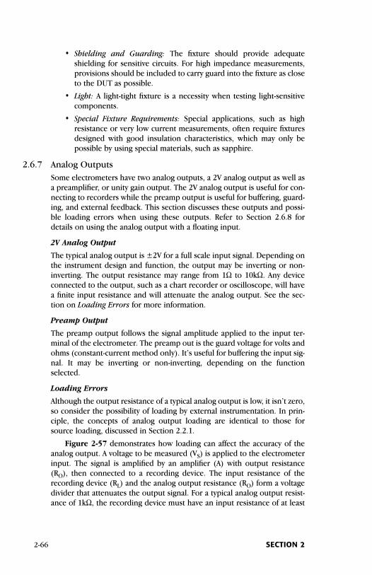
• Shielding and Guarding: The fixture should provide adequateshielding for sensitive circuits. For high impedance measurements,provisions should be included to carry guard into the fixture as closeto the DUT as possible.
• Light: A light-tight fixture is a necessity when testing light-sensitivecomponents.
• Special Fixture Requirements: Special applications, such as highresistance or very low current measurements, often require fixturesdesigned with good insulation characteristics, which may only bepossible by using special materials, such as sapphire.
2.6.7 Analog OutputsSome electrometers have two analog outputs, a 2V analog output as well asa preamplifier, or unity gain output. The 2V analog output is useful for con-necting to recorders while the preamp output is useful for buffering, guard-ing, and external feedback. This section discusses these outputs and possi-ble loading errors when using these outputs. Refer to Section 2.6.8 fordetails on using the analog output with a floating input.
2V Analog Output
The typical analog output is ±2V for a full scale input signal. Depending onthe instrument design and function, the output may be inverting or non-inverting. The output resistance may range from 1Ω to 10kΩ. Any deviceconnected to the output, such as a chart recorder or oscilloscope, will havea finite input resistance and will attenuate the analog output. See the sec-tion on Loading Errors for more information.
Preamp Output
The preamp output follows the signal amplitude applied to the input ter-minal of the electrometer. The preamp out is the guard voltage for volts andohms (constant-current method only). It’s useful for buffering the input sig-nal. It may be inverting or non-inverting, depending on the functionselected.
Loading Errors
Although the output resistance of a typical analog output is low, it isn’t zero,so consider the possibility of loading by external instrumentation. In prin-ciple, the concepts of analog output loading are identical to those forsource loading, discussed in Section 2.2.1.
Figure 2-57 demonstrates how loading can affect the accuracy of theanalog output. A voltage to be measured (VS) is applied to the electrometerinput. The signal is amplified by an amplifier (A) with output resistance(RO), then connected to a recording device. The input resistance of therecording device (RL) and the analog output resistance (RO) form a voltagedivider that attenuates the output signal. For a typical analog output resist-ance of 1kΩ, the recording device must have an input resistance of at least
2-66 SECTION 2
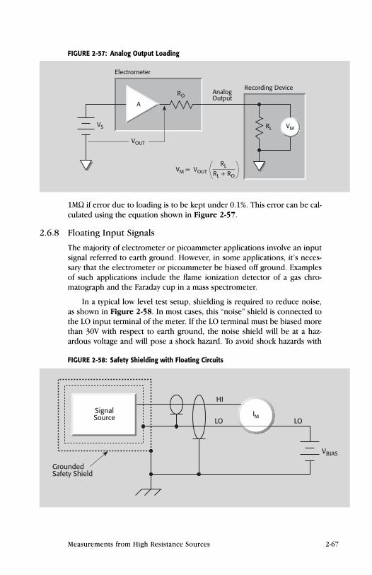
1MΩ if error due to loading is to be kept under 0.1%. This error can be cal-culated using the equation shown in Figure 2-57.
2.6.8 Floating Input Signals
The majority of electrometer or picoammeter applications involve an inputsignal referred to earth ground. However, in some applications, it’s neces-sary that the electrometer or picoammeter be biased off ground. Examplesof such applications include the flame ionization detector of a gas chro-matograph and the Faraday cup in a mass spectrometer.
In a typical low level test setup, shielding is required to reduce noise,as shown in Figure 2-58. In most cases, this “noise” shield is connected tothe LO input terminal of the meter. If the LO terminal must be biased morethan 30V with respect to earth ground, the noise shield will be at a haz-ardous voltage and will pose a shock hazard. To avoid shock hazards with
Measurements from High Resistance Sources 2-67
FIGURE 2-57: Analog Output Loading
A
VS
Electrometer
RO
RL VM
AnalogOutput
Recording Device
VOUT
VM = VOUTRL
RL + RO
FIGURE 2-58: Safety Shielding with Floating Circuits
VBIAS
HI
LOIM
LOSignalSource
GroundedSafety Shield
floating circuits, a second grounded safety shield must be added to enclosethe noise shield completely.
Most picoammeters and electrometers use a triaxial input connectorwith the outside shield connected to earth ground for safety. By using a tri-axial connector at the safety shield and a triaxial cable between the testsetup and the instrument, a completely shielded and safe system will result.Note: Maximum float voltage ratings must be observed to prevent break-down between the inner conductors and the outer grounded shield.
For SMUs with the outside shield connected to LO and for picoamme-ters with a coax input, the input should not be allowed to float more than30Vrms (42V peak) from ground.
2.6.9 Electrometer VerificationAll measuring instruments require periodic recalibration, typically once peryear. It may be desirable to check the functions of the instrument more fre-quently. This section describes simple tests to verify electrometer functions.
Amperes
First, turn the power on and allow the meter to warm up for the time spec-ified in the service manual. Then place a shield cap over the input connec-tor and link the low impedance input terminal to ground. The zero checkshould be enabled. Next, set the meter to the most sensitive current range,zero the meter, and then disable the zero-check switch. After several sec-onds, the meter reading should settle to within a few digits. The indicatedcurrent is the input offset. If it exceeds the instrument specification by 25%or so, leave the power on overnight and repeat the test. If the current is stillexcessive, the instrument should be repaired.
The ammeter input should never be short-circuited because itwill then have no negative feedback. While no damage will occur, theresult will be meaningless.
Volts
A single flashlight cell or a 9V battery will give a rough check on the voltagefunction. (Be sure to try both polarities.)
Ohms
The ohms function can be checked with almost any known resistor, but it’sbest to use as high a resistance as possible.
Coulombs
The coulombs function can be checked using a low leakage capacitor and avoltage source. A known capacitor in the range of 100pF to 1000pF can becharged to a known voltage via a flashlight cell. The capacitor is then con-nected to the electrometer input after setting the meter to coulombs anddisabling the zero check switch. Conversely, this procedure can be used todetermine the value of the capacitor.
2-68 SECTION 2
S E C T I O N 3
Measurements fromLow Resistance
Sources
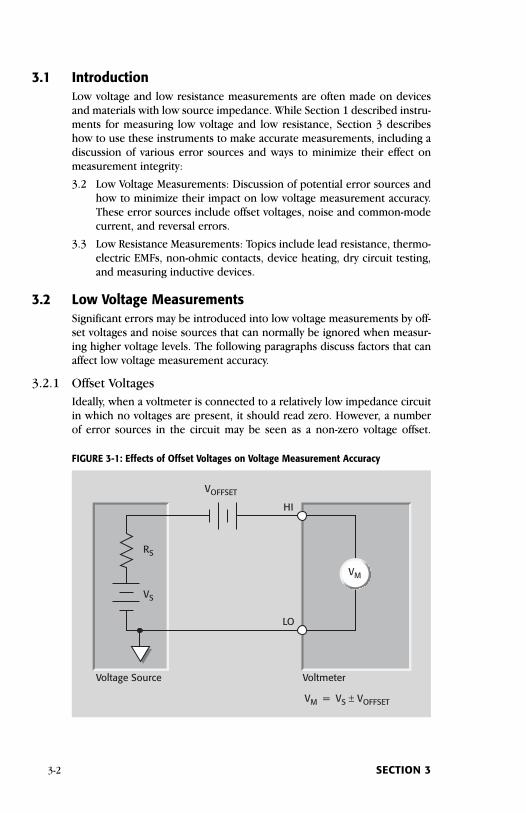
3.1 IntroductionLow voltage and low resistance measurements are often made on devicesand materials with low source impedance. While Section 1 described instru-ments for measuring low voltage and low resistance, Section 3 describeshow to use these instruments to make accurate measurements, including adiscussion of various error sources and ways to minimize their effect onmeasurement integrity:
3.2 Low Voltage Measurements: Discussion of potential error sources andhow to minimize their impact on low voltage measurement accuracy.These error sources include offset voltages, noise and common-modecurrent, and reversal errors.
3.3 Low Resistance Measurements: Topics include lead resistance, thermo-electric EMFs, non-ohmic contacts, device heating, dry circuit testing,and measuring inductive devices.
3.2 Low Voltage MeasurementsSignificant errors may be introduced into low voltage measurements by off-set voltages and noise sources that can normally be ignored when measur-ing higher voltage levels. The following paragraphs discuss factors that canaffect low voltage measurement accuracy.
3.2.1 Offset VoltagesIdeally, when a voltmeter is connected to a relatively low impedance circuitin which no voltages are present, it should read zero. However, a numberof error sources in the circuit may be seen as a non-zero voltage offset.
3-2 SECTION 3
VS
RS
Voltage Source
VM
HI
LO
Voltmeter
VM = VS ± VOFFSET
VOFFSET
FIGURE 3-1: Effects of Offset Voltages on Voltage Measurement Accuracy
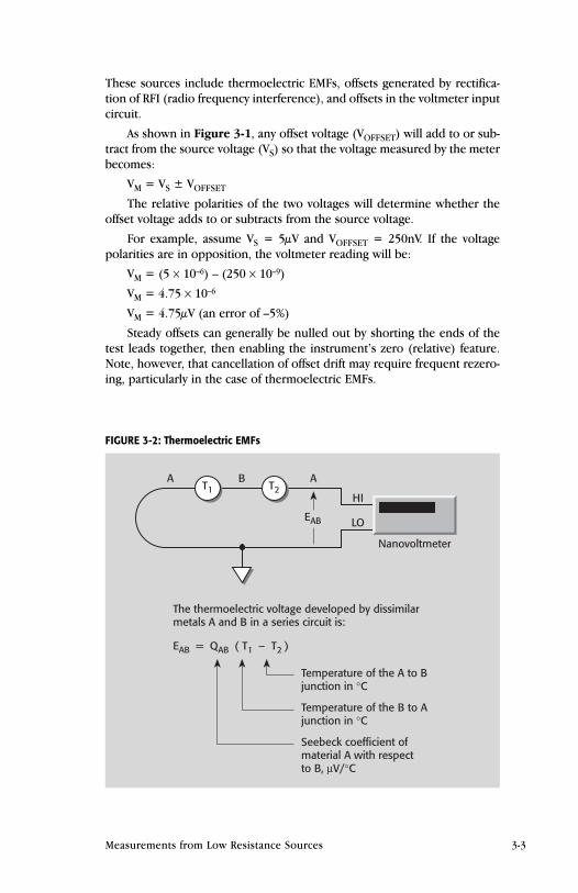
These sources include thermoelectric EMFs, offsets generated by rectifica-tion of RFI (radio frequency interference), and offsets in the voltmeter inputcircuit.
As shown in Figure 3-1, any offset voltage (VOFFSET) will add to or sub-tract from the source voltage (VS) so that the voltage measured by the meterbecomes:
VM = VS ± VOFFSET
The relative polarities of the two voltages will determine whether theoffset voltage adds to or subtracts from the source voltage.
For example, assume VS = 5µV and VOFFSET = 250nV. If the voltagepolarities are in opposition, the voltmeter reading will be:
VM = (5 × 10⁻⁶) – (250 × 10–9)
VM = 4.75 × 10⁻⁶
VM = 4.75µV (an error of –5%)
Steady offsets can generally be nulled out by shorting the ends of thetest leads together, then enabling the instrument’s zero (relative) feature.Note, however, that cancellation of offset drift may require frequent rezero-ing, particularly in the case of thermoelectric EMFs.
Measurements from Low Resistance Sources 3-3
Nanovoltmeter
T2
EAB
HI
LO
T1ABA
EAB = QAB ( T1 – T2 )
The thermoelectric voltage developed by dissimilarmetals A and B in a series circuit is:
Temperature of the A to Bjunction in °C
Temperature of the B to Ajunction in °C
Seebeck coefficient ofmaterial A with respectto B, µV/°C
FIGURE 3-2: Thermoelectric EMFs
Thermoelectric EMFs
Thermoelectric voltages (thermoelectric EMFs) are the most commonsource of errors in low voltage measurements. These voltages are generat-ed when different parts of a circuit are at different temperatures and whenconductors made of dissimilar materials are joined together, as shown inFigure 3-2. The Seebeck coefficients (QAB) of various materials with respectto copper are summarized in Table 3-1.
TABLE 3-1: Seebeck Coefficients
* Ag = silver Au = gold Cu = copper CuO = copper oxidePb = lead Si = silicon Sn = tin
Constructing circuits using the same material for all conductors mini-mizes thermoelectric EMF generation. For example, connections made bycrimping copper sleeves or lugs on copper wires results in copper-to-copper junctions, which generate minimal thermoelectric EMFs. Also, con-nections must be kept clean and free of oxides. Crimped copper-to-copperconnections, called “cold welded,” do not allow oxygen penetration andmay have a Seebeck coefficient of ≤0.2µV/°C, while Cu-CuO connectionsmay have a coefficient as high as 1mV/°C.
Minimizing temperature gradients within the circuit also reduces ther-moelectric EMFs. A technique for minimizing such gradients is to place cor-responding pairs of junctions in close proximity to one another and toprovide good thermal coupling to a common, massive heat sink. Electricalinsulators having high thermal conductivity must be used, but, since mostelectrical insulators don’t conduct heat well, special insulators such as hardanodized aluminum, beryllium oxide, specially filled epoxy resins, sapphire,or diamond must be used to couple junctions to the heat sink.
Allowing test equipment to warm up and reach thermal equilibrium ina constant ambient temperature also minimizes thermoelectric EMF effects.The instrument zero feature can compensate for any remaining thermo-electric EMF, provided it is relatively constant. To keep ambient tempera-tures constant, equipment should be kept away from direct sunlight,exhaust fans, and similar sources of heat flow or moving air. Wrapping con-nections in insulating foam (e.g., polyurethane) also minimizes ambienttemperature fluctuations caused by air movement.
Paired Materials* Seebeck Coefficient, QAB
Cu - Cu ≤0.2 µV/°CCu - Ag 0.3 µV/°CCu - Au 0.3 µV/°CCu - Pb/Sn 1–3 µV/°CCu - Si 400 µV/°CCu - Kovar ~40–75 µV/°CCu - CuO ~1000 µV/°C
3-4 SECTION 3
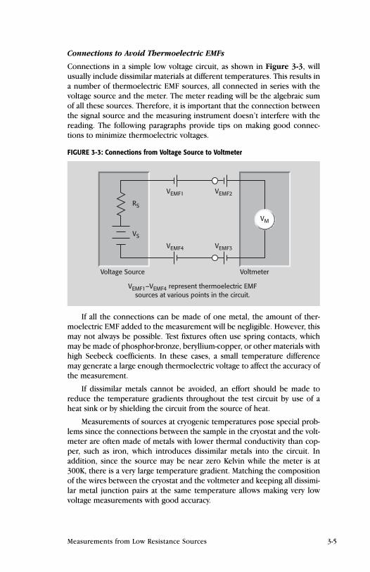
Connections to Avoid Thermoelectric EMFs
Connections in a simple low voltage circuit, as shown in Figure 3-3, willusually include dissimilar materials at different temperatures. This results ina number of thermoelectric EMF sources, all connected in series with thevoltage source and the meter. The meter reading will be the algebraic sumof all these sources. Therefore, it is important that the connection betweenthe signal source and the measuring instrument doesn’t interfere with thereading. The following paragraphs provide tips on making good connec-tions to minimize thermoelectric voltages.
FIGURE 3-3: Connections from Voltage Source to Voltmeter
If all the connections can be made of one metal, the amount of ther-moelectric EMF added to the measurement will be negligible. However, thismay not always be possible. Test fixtures often use spring contacts, whichmay be made of phosphor-bronze, beryllium-copper, or other materials withhigh Seebeck coefficients. In these cases, a small temperature differencemay generate a large enough thermoelectric voltage to affect the accuracy ofthe measurement.
If dissimilar metals cannot be avoided, an effort should be made toreduce the temperature gradients throughout the test circuit by use of aheat sink or by shielding the circuit from the source of heat.
Measurements of sources at cryogenic temperatures pose special prob-lems since the connections between the sample in the cryostat and the volt-meter are often made of metals with lower thermal conductivity than cop-per, such as iron, which introduces dissimilar metals into the circuit. Inaddition, since the source may be near zero Kelvin while the meter is at300K, there is a very large temperature gradient. Matching the compositionof the wires between the cryostat and the voltmeter and keeping all dissimi-lar metal junction pairs at the same temperature allows making very lowvoltage measurements with good accuracy.
VEMF1–VEMF4 represent thermoelectric EMFsources at various points in the circuit.
VS
RS
Voltage Source
VM
Voltmeter
VEMF1 VEMF2
VEMF4 VEMF3
Measurements from Low Resistance Sources 3-5
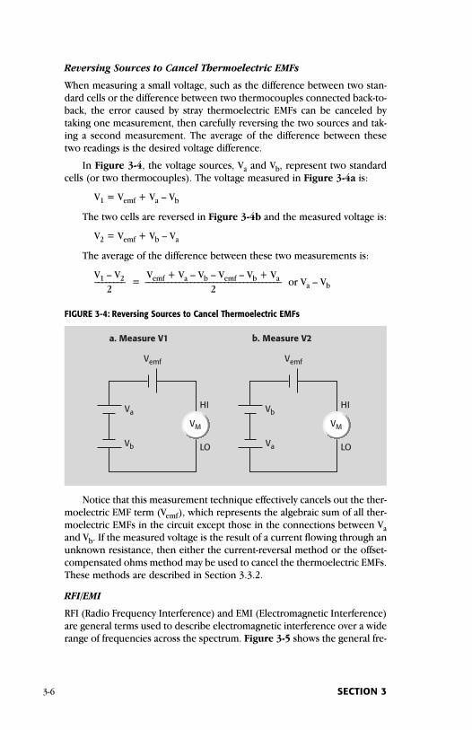
Reversing Sources to Cancel Thermoelectric EMFs
When measuring a small voltage, such as the difference between two stan-dard cells or the difference between two thermocouples connected back-to-back, the error caused by stray thermoelectric EMFs can be canceled bytaking one measurement, then carefully reversing the two sources and tak-ing a second measurement. The average of the difference between thesetwo readings is the desired voltage difference.
In Figure 3-4, the voltage sources, Va and Vb, represent two standardcells (or two thermocouples). The voltage measured in Figure 3-4a is:
V1 = Vemf + Va – Vb
The two cells are reversed in Figure 3-4b and the measured voltage is:
V2 = Vemf + Vb – Va
The average of the difference between these two measurements is:
V1 – V2 Vemf + Va – Vb – Vemf – Vb + Va________ = ____________________________________ or Va – Vb2 2
FIGURE 3-4: Reversing Sources to Cancel Thermoelectric EMFs
Notice that this measurement technique effectively cancels out the ther-moelectric EMF term (Vemf), which represents the algebraic sum of all ther-moelectric EMFs in the circuit except those in the connections between Vaand Vb. If the measured voltage is the result of a current flowing through anunknown resistance, then either the current-reversal method or the offset-compensated ohms method may be used to cancel the thermoelectric EMFs.These methods are described in Section 3.3.2.
RFI/EMI
RFI (Radio Frequency Interference) and EMI (Electromagnetic Interference)are general terms used to describe electromagnetic interference over a widerange of frequencies across the spectrum. Figure 3-5 shows the general fre-
Va
VM
Vb
Vemf
HI
LO
a. Measure V1 b. Measure V2
Vb
VM
Va
Vemf
HI
LO
3-6 SECTION 3
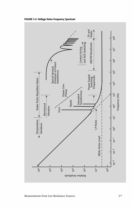
Measurements from Low Resistance Sources 3-7
10–3
Freq
uenc
y(H
z)
10–2
10–1
100
101
102
103
104
105
106
107
108
100
101
102
103
104
105
106
Relative Amplitude
Whi
teN
oise
Leve
l1/
fNoi
se
Rada
rPu
lse
Repe
titio
nRa
tes
Mec
hani
cal
Vibr
atio
n
Hum
Ripp
le
Satu
rate
dTr
ansf
orm
ers
Con
tact
Arci
ng
and
SCR
Switc
hing
TVan
dRa
dar
AM/F
MB
road
cast
sPo
wer
Supp
lySw
itchi
ngFr
eque
ncie
s
Pow
erLi
nePi
ckup
Typi
calS
pect
ral
Enve
lope
ofPu
lsed
Inte
rfer
ence
Tem
pera
ture
Varia
tions
FIGURE 3-5: Voltage Noise Frequency Spectrum
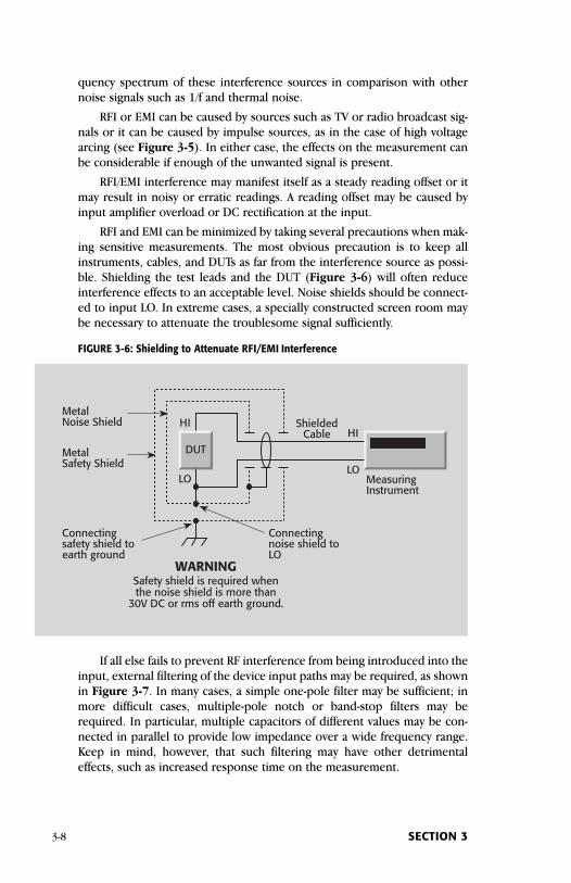
quency spectrum of these interference sources in comparison with othernoise signals such as 1/f and thermal noise.
RFI or EMI can be caused by sources such as TV or radio broadcast sig-nals or it can be caused by impulse sources, as in the case of high voltagearcing (see Figure 3-5). In either case, the effects on the measurement canbe considerable if enough of the unwanted signal is present.
RFI/EMI interference may manifest itself as a steady reading offset or itmay result in noisy or erratic readings. A reading offset may be caused byinput amplifier overload or DC rectification at the input.
RFI and EMI can be minimized by taking several precautions when mak-ing sensitive measurements. The most obvious precaution is to keep allinstruments, cables, and DUTs as far from the interference source as possi-ble. Shielding the test leads and the DUT (Figure 3-6) will often reduceinterference effects to an acceptable level. Noise shields should be connect-ed to input LO. In extreme cases, a specially constructed screen room maybe necessary to attenuate the troublesome signal sufficiently.
If all else fails to prevent RF interference from being introduced into theinput, external filtering of the device input paths may be required, as shownin Figure 3-7. In many cases, a simple one-pole filter may be sufficient; inmore difficult cases, multiple-pole notch or band-stop filters may berequired. In particular, multiple capacitors of different values may be con-nected in parallel to provide low impedance over a wide frequency range.Keep in mind, however, that such filtering may have other detrimentaleffects, such as increased response time on the measurement.
3-8 SECTION 3
FIGURE 3-6: Shielding to Attenuate RFI/EMI Interference
MeasuringInstrument
HI
LOLO
ShieldedCable
MetalNoise Shield
MetalSafety Shield
Connectingsafety shield toearth ground
Connectingnoise shield toLO
WARNINGSafety shield is required whenthe noise shield is more than
30V DC or rms off earth ground.
HI
DUT
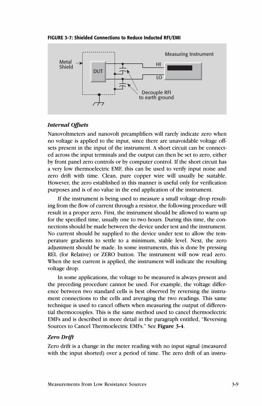
Internal Offsets
Nanovoltmeters and nanovolt preamplifiers will rarely indicate zero whenno voltage is applied to the input, since there are unavoidable voltage off-sets present in the input of the instrument. A short circuit can be connect-ed across the input terminals and the output can then be set to zero, eitherby front panel zero controls or by computer control. If the short circuit hasa very low thermoelectric EMF, this can be used to verify input noise andzero drift with time. Clean, pure copper wire will usually be suitable.However, the zero established in this manner is useful only for verificationpurposes and is of no value in the end application of the instrument.
If the instrument is being used to measure a small voltage drop result-ing from the flow of current through a resistor, the following procedure willresult in a proper zero. First, the instrument should be allowed to warm upfor the specified time, usually one to two hours. During this time, the con-nections should be made between the device under test and the instrument.No current should be supplied to the device under test to allow the tem-perature gradients to settle to a minimum, stable level. Next, the zeroadjustment should be made. In some instruments, this is done by pressingREL (for Relative) or ZERO button. The instrument will now read zero.When the test current is applied, the instrument will indicate the resultingvoltage drop.
In some applications, the voltage to be measured is always present andthe preceding procedure cannot be used. For example, the voltage differ-ence between two standard cells is best observed by reversing the instru-ment connections to the cells and averaging the two readings. This sametechnique is used to cancel offsets when measuring the output of differen-tial thermocouples. This is the same method used to cancel thermoelectricEMFs and is described in more detail in the paragraph entitled, “ReversingSources to Cancel Thermoelectric EMFs.” See Figure 3-4.
Zero Drift
Zero drift is a change in the meter reading with no input signal (measuredwith the input shorted) over a period of time. The zero drift of an instru-
Measurements from Low Resistance Sources 3-9
FIGURE 3-7: Shielded Connections to Reduce Inducted RFI/EMI
Measuring Instrument
HI
LO
Decouple RFIto earth ground
MetalShield
DUT
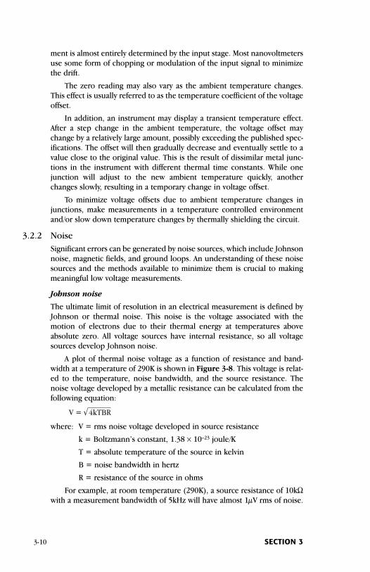
ment is almost entirely determined by the input stage. Most nanovoltmetersuse some form of chopping or modulation of the input signal to minimize the drift.
The zero reading may also vary as the ambient temperature changes.This effect is usually referred to as the temperature coefficient of the voltageoffset.
In addition, an instrument may display a transient temperature effect.After a step change in the ambient temperature, the voltage offset maychange by a relatively large amount, possibly exceeding the published spec-ifications. The offset will then gradually decrease and eventually settle to avalue close to the original value. This is the result of dissimilar metal junc-tions in the instrument with different thermal time constants. While onejunction will adjust to the new ambient temperature quickly, anotherchanges slowly, resulting in a temporary change in voltage offset.
To minimize voltage offsets due to ambient temperature changes injunctions, make measurements in a temperature controlled environmentand/or slow down temperature changes by thermally shielding the circuit.
3.2.2 NoiseSignificant errors can be generated by noise sources, which include Johnsonnoise, magnetic fields, and ground loops. An understanding of these noisesources and the methods available to minimize them is crucial to makingmeaningful low voltage measurements.
Johnson noise
The ultimate limit of resolution in an electrical measurement is defined byJohnson or thermal noise. This noise is the voltage associated with themotion of electrons due to their thermal energy at temperatures aboveabsolute zero. All voltage sources have internal resistance, so all voltagesources develop Johnson noise.
A plot of thermal noise voltage as a function of resistance and band-width at a temperature of 290K is shown in Figure 3-8. This voltage is relat-ed to the temperature, noise bandwidth, and the source resistance. Thenoise voltage developed by a metallic resistance can be calculated from thefollowing equation:
where: V = rms noise voltage developed in source resistance
k = Boltzmann’s constant, 1.38 × 10⁻²³ joule/K
T = absolute temperature of the source in kelvin
B = noise bandwidth in hertz
R = resistance of the source in ohms
For example, at room temperature (290K), a source resistance of 10kΩwith a measurement bandwidth of 5kHz will have almost 1µV rms of noise.
V = 4kTBR
3-10 SECTION 3

Johnson noise may be reduced by lowering the temperature of thesource resistance and by decreasing the bandwidth of the measurement.Cooling the sample from room temperature (290K) to liquid nitrogen tem-perature (77K) decreases the voltage noise by approximately a factor of two.
If the voltmeter has adjustable filtering and integration, the bandwidthcan be reduced by increasing the amount of filtering and/or by integratingover multiple power line cycles. Decreasing the bandwidth of the measure-ment is equivalent to increasing the response time of the instrument, andas a result, the measurement time is much longer. However, if the mea-surement response time is long, the thermoelectric EMFs associated withthe temperature gradients in the circuit become more important. Sensitivemeasurements may not be achieved if the thermal time constants of themeasurement circuit are of the same order as the response time. If thisoccurs, distinguishing between a change in signal voltage and a change inthermoelectric EMFs becomes impossible.
Johnson noise is discussed in more detail in Section 2.6.5.
Magnetic Fields
Magnetic fields generate error voltages in two circumstances: 1) if the fieldis changing with time, and 2) if there is relative motion between the circuitand the field. Voltages in conductors can be generated from the motion ofa conductor in a magnetic field, from local AC currents caused by compo-nents in the test system, or from the deliberate ramping of the magnetic
Measurements from Low Resistance Sources 3-11
FIGURE 3-8: Thermal Noise Voltage as a Function of Resistance and Bandwidth
100
10
1.0
0.1
0.010.01 0.1 1.0 10 1000
Thermal NoiseVoltage Vt
Bandwidth1MHz
100kHz
10kHz
1kHz
100Hz
V = 4kTBRwhere 4kT = 1.6 × 10⁻²⁰
at 17°C (290K)
Reproduced from:Henry W. Ott, NoiseReduction Techniques inElectronic Systems, 2ndEdition, New York: Wiley-Interscience, 1988
100
field, such as for magneto-resistance measurements. Even the earth’s rela-tively weak magnetic field can generate nanovolts in dangling leads, so leadsmust be kept short and rigidly tied down.
Basic physics shows that the amount of voltage a magnetic field inducesin a circuit is proportional to the area the circuit leads enclose and the rateof change in magnetic flux density, as shown in Figure 3-9. The inducedvoltage (VB) is calculated as follows:
The induced voltage is proportional both to the magnitude of A and, as well as to the rate of change in A and , so there are two ways to min-
imize the induced voltage:
• Keep both A and to a minimum by reducing loop area and avoid-ing magnetic fields, if possible; and
• Keep both A and constant by minimizing vibration and movement,and by keeping circuits away from AC and RF fields.
To minimize induced magnetic voltages, leads must be run close togeth-er and magnetically shielded and they should be tied down to minimizemovement. Mu-metal, a special alloy with high permeability at low magnet-ic flux densities and at low frequencies, is a commonly used magneticshielding material.
B
B
BB
dφdt
d(BA)VB =dt
dAdt dt
= = B + A dB
where: VB = induced voltageA = loop areaB = magnetic flux density
φ = BA = magnetic flux
3-12 SECTION 3
Voltmeter
Area A(enclosed)
The voltage developed due to a field passingthrough a circuit enclosing a prescribed area is:
B
VB =dt
d (BA)dt
dAdt
dBdt
= = B + Ad
FIGURE 3-9: Low Voltages Generated by Magnetic Fields
Figure 3-10 shows two ways of locating the leads from the source tothe voltmeter. In Figure 3-10a, a large area is enclosed; thus, a large volt-age is developed. In Figure 3-10b, a much smaller area is enclosed becausethe leads are twisted together, and the voltage induced is considerablyreduced. Twisted pair also cancels magnetically induced voltages becauseeach adjacent twist couples a small but alternating polarity (equal) voltage.
Conductors that carry large currents should also be shielded or run astwisted pairs to avoid generating magnetic fields that can affect nearby cir-cuits. In addition to these techniques, AC signals from magnetic fields canbe filtered at the input of the instrument. If possible, the signal source andthe instrument should be physically relocated further away from the inter-fering magnetic field.
Ground Loops
Noise and error voltages also arise from ground loops. When there are twoconnections to earth, such as when the source and measuring instrumentsare both connected to a common ground bus, a loop is formed as shown inFigure 3-11a. A voltage (VG) between the source and instrument groundswill cause a current (I) to flow around the loop. This current will create anunwanted voltage in series with the source voltage. From Ohm’s Law:
VG = IR
where VG = ground loop interfering voltage, R = the resistance in the sig-nal path through which the ground loop current flows, and I = the groundloop current. A typical example of a ground loop can be seen when a num-ber of instruments are plugged into power strips on different instrumentracks. Frequently, there is a small difference in potential between theground points. This potential difference can cause large currents to circu-late and create unexpected voltage drops.
Measurements from Low Resistance Sources 3-13
Voltmeter
Source
VoltmeterSource
b.
a.
FIGURE 3-10: Minimizing Interference from Magnetic Fields
The cure for such ground loops is to ground all equipment at a singlepoint. The easiest way of accomplishing this is to use isolated power sourcesand instruments, then find a single, good earth-ground point for the entiresystem. Avoid connecting sensitive instruments to the same ground system
3-14 SECTION 3
Experiment(source) VS R
VIN
HI
Nanovoltmeter
LO
IGround 2
Ground bus
VG
Input voltage to the nanovoltmeter is:
VIN = VS + VG
where VG = IR, andR = Resistance of input LO connection (typically
around 100mΩ)I = Current passing through input LO connection
due to ground voltages (VG) in the ground bus(magnitude may be amperes)
VS = Source voltage (desired signal)VG may exceed VS by orders of magnitude.
Ground 1
FIGURE 3-11a: Multiple Grounds (Ground Loops)
Experiment(source) VS
RVIN
HI
Nanovoltmeter
LO
ZCM
I
Ground bus
VG
VIN ≈ VS, since VG is now insignificant compared to VS.
ZCM = Common mode impedance of nanovoltmeter
FIGURE 3-11b: Reduced Ground Loops
used by other instruments, machinery, or other high power equipment. Asshown in Figure 3-11b, ground loops can also be reduced by using a volt-meter with high common mode impedance (ZCM), also known as commonmode isolation.
3.2.3 Common-Mode Current and Reversal ErrorsExcessive common-mode current can significantly affect low-level voltagemeasurements. Although common-mode currents are most often associatedwith noise problems, they can result in large DC offsets in some cases. Inthe following paragraphs, we will briefly discuss the basic principles behinderrors generated by common-mode currents and ways to avoid lead rever-sal errors.
Common-Mode Current
Common-mode current is the current that flows between the instrument’sLO terminal and chassis or earth ground. As shown in Figure 3-12, com-mon-mode current (ICM) is caused by capacitive coupling (CCOUPLING) fromthe power line through the power transformer. The amplitude of the com-mon-mode current is defined as:
ICM = 2π fCCOUPLING (V2 ± V1)
where f is the power line frequency.
Note that the common-mode current flows through the impedance(ZCM), which is present between input LO and chassis ground. As a result,the amplitude of voltage (VCM) depends on the magnitude of ZCM as well asthe value of ICM.
Measurements from Low Resistance Sources 3-15
LO
ZCM
VCM
V1 CCOUPLING
V2
ICM
Line
Neutral
Voltmeter Power Supply
ICM = 2πf CCOUPLING (V2 ± 1)
FIGURE 3-12: Common Mode Current Generation by Power Line Coupling

Common-Mode Reversal Errors
Reversing leads can result in errors caused by common-mode currents. Asshown in Figure 3-13, many low voltage sources have internal resistivedividers, which attenuate an internal voltage source to the desired level. Forexample, the output voltage from the source is defined as:
R2VOUTPUT = VS_________( R1 + R2
)With the correct connection scheme shown in Figure 3-13a, the low or
chassis side of the voltage source is connected to input LO of the measur-ing instrument. Any common-mode current (ICM) that may be present flowsfrom the voltmeter input LO to instrument chassis common, through earthground to voltage source ground. Note that no common-mode currentflows through either of the two divider resistors of the voltage source whenthis connection scheme is used.
If the input leads of the voltmeter are reversed, we have the situationshown in Figure 3-13b. Now, the common-mode current (ICM) flowsthrough R2, developing a voltage drop, which is added to the voltage to bemeasured. This added voltage is mainly power line frequency and its effecton the voltmeter reading will depend upon the normal-mode rejectioncapability of the meter. The reading may become noisy or it may have a con-stant offset. In some cases, the sensitivity of the meter may be reduced,because the input stages are overloaded.
To minimize common-mode reversal errors, choose an instrument withthe lowest possible common-mode current. If possible, the voltage sourcebeing measured should be isolated from ground.
3.3 Low Resistance MeasurementsAside from all the low voltage measurement considerations described inSection 3.2, low resistance measurements are subject to additional errorsources, including lead resistance, non-ohmic contacts, and device heating.This section describes these error sources and methods to eliminate or min-imize them. Other measurement considerations, including dry circuit test-ing and testing inductive devices, are also described.
3.3.1 Lead Resistance and Four-Wire Method
Resistance measurements are often made using the two-wire method shownin Figure 3-14. The test current is forced through the test leads and theresistance (R) being measured. The meter then measures the voltage acrossthe resistance through the same set of test leads and computes the resis-tance value accordingly.
The main problem with the two-wire method as applied to low resis-tance measurements is that the total lead resistance (RLEAD) is added to themeasurement. Since the test current (I) causes a small but significant volt-
3-16 SECTION 3
Measurements from Low Resistance Sources 3-17
Low voltage sourceusing resistive divider
VS
R1
R2
HI
ICM
LO
Voltmeter
a. With proper connections, ICM generates no noise or offset.
Low voltage sourceusing resistive divider
VS
R1
R2
HI
ICM
LO
Voltmeter
b. With reversed connections, ICM generates noise and possible offset.
VM
VM
ICM
ICM
FIGURE 3-13: Effects of Reversing Leads on Common Mode Errors

3-18 SECTION 3
Measured Resistance =I
VM = R + (2 × RLEAD)
Test Current (I)RLEAD
I VM
HI
LO
VM
RLEAD
VR R ResistanceUnder Test
LeadResistances
DMM
VM = Voltage measured by meterVR = Voltage across resistor
FIGURE 3-14: Two-Wire Resistance Measurement
Test Current (I)
RLEAD
I VM
Sense HI
Sense LO
VM
RLEAD
VR R ResistanceUnder Test
LeadResistances
DMM or Micro-ohmmeter
VM = Voltage measured by meterVR = Voltage across resistor (R)Because sense current is negligible, VM = VR
RLEAD
RLEADSource HI
Source LO
Sense Current (pA)
=I
VMand measured resistance =I
VR
FIGURE 3-15: Four-Wire Resistance Measurement
age drop across the lead resistances, the voltage (VM) measured by themeter won’t be exactly the same as the voltage (VR) directly across the testresistance (R), and considerable error can result. Typical lead resistances liein the range of 1mΩ to 10mΩ, so it’s very difficult to obtain accurate two-wire resistance measurements when the resistance under test is lower than10Ω to 100Ω (depending on lead resistance).
Due to the limitations of the two-wire method, the four-wire (Kelvin)connection method shown in Figure 3-15 is generally preferred for lowresistance measurements. These measurements can be made using a DMM,micro-ohmmeter, or a separate current source and voltmeter. With this con-figuration, the test current (I) is forced through the test resistance (R)through one set of test leads, while the voltage (VM) across the DUT is meas-ured through a second set of leads called sense leads. Although some smallcurrent may flow through the sense leads, it is usually negligible and cangenerally be ignored for all practical purposes. The voltage drop across thesense leads is negligible, so the voltage measured by the meter (VM) is essen-tially the same as the voltage (VR) across the resistance (R). Consequently,the resistance value can be determined much more accurately than with thetwo-wire method. Note that the voltage-sensing leads should be connectedas close to the resistor under test as possible to avoid including the resist-ance of the test leads in the measurement.
3.3.2 Thermoelectric EMFs and Offset Compensation MethodsThermoelectric voltages, as described in Section 3.2.1, can seriously affectlow resistance measurement accuracy. The current-reversal method, thedelta method, and the offset-compensated ohms method are three commonways to overcome these unwanted offsets.
Current-Reversal Method
Thermoelectric EMFs can be canceled by making two measurements withcurrents of opposite polarity, as shown in Figure 3-16. In this diagram, avoltmeter with a separate bipolar current source is used. With the positivecurrent applied as in Figure 3-16a, the measured voltage is:
VM+ = VEMF + IR
Reversing the current polarity as shown in Figure 3-16b yields the fol-lowing voltage measurement:
VM– = VEMF – IR
The two measurements can be combined to cancel thermoelectricEMFs:
VM+ – VM– (VEMF + IR) – (VEMF – IR)VM = ___________ = ____________________________ = IR
2 2The measured resistance is computed in the usual manner:
VMR = ___I
Measurements from Low Resistance Sources 3-19
Note that the thermoelectric voltage (VEMF) is completely canceled outby this method of resistance calculation.
For the current-reversal method to be effective, it’s important to use alow noise voltmeter with a response speed that is fast compared with thethermal time constant of the circuit under test. If the response speed is tooslow, any changes in the circuit temperature during the measurement cyclewill cause changes in the thermoelectric EMFs that won’t be completely can-celed, and some error will result.
Delta Method
When the thermoelectric voltages are constant with respect to the measure-ment cycle, the current-reversal method will successfully compensate forthese offsets. However, if changing thermoelectric voltages are causing inac-curate results, then the delta method should be used. The delta method issimilar to the current-reversal method in terms of alternating the currentsource polarity, but it differs in that it uses three voltage measurements tomake each resistance calculation. This method can best be explainedthrough an illustration and mathematical computations.
Figure 3-17 shows the voltage drop of a DUT as a function of time withan alternating polarity current applied. A voltage measurement (VM1, VM2,VM3, etc.) is taken each time the polarity is changed. Each voltage measure-ment includes a constant thermal voltage offset (VEMF) and a linearly chang-ing voltage offset (δV). The thermal voltage drift may be approximated as alinear function over short periods, so the rate of change of voltage as a func-tion of time (δV) can also be treated as a constant. The first three voltagemeasurements include the following voltages:
3-20 SECTION 3
VM = = I RVM+ – VM–
2
a. Measurement with Positive Polarity
R
VEMF
I VM+
VM+ = VEMF + I R
b. Measurement with Negative Polarity
R
VEMF
I VM–
VM– = VEMF – I R
FIGURE 3-16: Canceling Thermoelectric EMFs with Current Reversal
VM1 = V1 + VEMF
VM2 = V2 + VEMF + δV
VM3 = V3 + VEMF + 2δV
where: VM1, VM2, and VM3 are voltage measurements
VM1 is presumed to be taken at time = 0
V1, V2, and V3 are the voltage drop of the DUT due to the appliedcurrent
VEMF is the constant thermoelectric voltage offset at the time theVM1 measurement is taken
δV is the thermoelectric voltage change
Cancellation of both the thermoelectric voltage offset (VEMF) term andthe thermoelectric voltage change (δV) term is possible through mathemat-ical computation using three voltage measurements. First, take one-half thedifference of the first two voltage measurements and call this term VA:
VM1–VM2 (V1+VEMF) – (V2+VEMF+δV) (V1–V2) δVVA = __________ = _______________________________ = ________ – ___
2 2 2 2
Then, take one-half the difference of the second (VM2) and third (VM3) volt-age measurements and call this term VB:
VM3–VM2 (V3+VEMF+2δV) – (V2+VEMF+δV) (V3–V2) δVVB = __________ = _____________________________________ = ________ – ___
2 2 2 2
Measurements from Low Resistance Sources 3-21
FIGURE 3-17: Canceling Thermoelectric EMFs with Delta Method
VEMF
DUTVoltage
VM1
VM3
VM2
TestCurrent
δV = linearly changingthermoelectricvoltages
Time
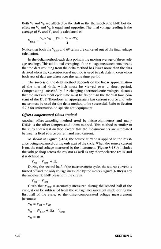
Both VA and VB are affected by the drift in the thermoelectric EMF, but theeffect on VA and VB is equal and opposite. The final voltage reading is theaverage of VA and VB and is calculated as:
VA – VB (V1 + V3 – 2V2)VFinal = ________ = _________________
2 4
Notice that both the VEMF and δV terms are canceled out of the final voltagecalculation.
In the delta method, each data point is the moving average of three volt-age readings. This additional averaging of the voltage measurements meansthat the data resulting from the delta method has lower noise than the dataderived when the current-reversal method is used to calculate it, even whenboth sets of data are taken over the same time period.
The success of the delta method depends on the linear approximationof the thermal drift, which must be viewed over a short period.Compensating successfully for changing thermoelectric voltages dictatesthat the measurement cycle time must be faster than the thermal time con-stant of the DUT. Therefore, an appropriately fast current source and volt-meter must be used for the delta method to be successful. Refer to Section4.7.2 for information on specific test equipment.
Offset-Compensated Ohms Method
Another offset-canceling method used by micro-ohmmeters and manyDMMs is the offset-compensated ohms method. This method is similar tothe current-reversal method except that the measurements are alternatedbetween a fixed source current and zero current.
As shown in Figure 3-18a, the source current is applied to the resist-ance being measured during only part of the cycle. When the source currentis on, the total voltage measured by the instrument (Figure 3-18b) includesthe voltage drop across the resistor as well as any thermoelectric EMFs, andit is defined as:
VM1 = VEMF + IR
During the second half of the measurement cycle, the source current isturned off and the only voltage measured by the meter (Figure 3-18c) is anythermoelectric EMF present in the circuit:
VM2 = VEMF
Given that VEMF is accurately measured during the second half of thecycle, it can be subtracted from the voltage measurement made during thefirst half of the cycle, so the offset-compensated voltage measurementbecomes:
VM = VM1 – VM2
VM = (VEMF + IR) – VEMF
VM = IR
3-22 SECTION 3

and,VMR = ___I
Again, note that the measurement process cancels the thermoelectricEMF term (VEMF).
FIGURE 3-18: Offset-Compensated Ohms Measurement
3.3.3 Non-Ohmic ContactsNon-ohmic contacts are evident when the potential difference across thecontact isn’t linearly proportional to the current flowing through it. Non-ohmic contacts may occur in a low voltage circuit as a result of oxide filmsor other non-linear connections. A non-ohmic connection is likely to recti-fy any radio frequency energy (RFI) present, causing an offset voltage toappear in the circuit. (A further discussion on RFI can be found in Section3.2.1.) There are several ways to check for non-ohmic contacts and methodsto reduce them.
a. Offset compensationmeasurement cycle
SourceCurrent
Thermal offsetmeasurement
On
Onemeasurement
cycle
b. Voltage measurement withsource current on
R
VEMF
IVM1
VM1 = VEMF + IR
c. Voltage measurement withsource current off
R
VEMF
VM2
VM2 = VEMF
VM = (VM1 – VM2) = IR
Measurements from Low Resistance Sources 3-23
If using a micro-ohmmeter or DMM to make low resistance measure-ments, change the range to check for non-ohmic contacts. Changing themeasurement range usually changes the test current as well. A normal con-dition would indicate the same reading but with higher or lower resolution,depending on whether the instrument was up or down ranged. If the read-ing is significantly different, this may indicate a non-ohmic condition.
If using a separate current source and voltmeter to make low resistancemeasurements, each instrument must be checked for non-ohmic contacts. Ifthe current source contacts are non-ohmic, there may be a significant differ-ence in the compliance voltage when the source polarity is reversed. If thevoltmeter contacts are non-ohmic, they may rectify any AC pickup presentand cause a DC offset error. If this is the case, the offset compensated ohmsmethod is preferred to the current-reversal method for canceling offsets.
To prevent non-ohmic contacts, choose an appropriate contact materi-al, such as indium or gold. Make sure the compliance voltage is high enoughto avoid problems due to source contact non-linearity. To reduce error dueto voltmeter non-ohmic contacts, use shielding and appropriate groundingto reduce AC pickup.
3.3.4 Device Heating
Device heating can be a consideration when making resistance measure-ments on temperature-sensitive devices such as thermistors. The test cur-rents used for low resistance measurements are often much higher than thecurrents used for high resistance measurements, so power dissipation in thedevice can be a consideration if it is high enough to cause the device’s resist-ance value to change.
Recall that the power dissipation in a resistor is given by this formula:
P = I2R
From this relationship, we see that the power dissipated in the deviceincreases by a factor of four each time the current doubles. Thus, one wayto minimize the effects of device heating is to use the lowest current possi-ble while still maintaining the desired voltage across the device being test-ed. If the current cannot be reduced, use a narrow current pulse and a fastresponding voltmeter.
Most micro-ohmmeters and DMMs don’t have provisions for setting thetest current. It is generally determined by the range. In those cases, alter-nate means must be found to minimize device heating. One simple buteffective way to do so is to use the instrument’s one-shot trigger mode dur-ing measurements. While in this mode, the instrument will apply only a sin-gle, brief current pulse to the DUT during the measurement cycle, therebyminimizing errors caused by device heating.
3-24 SECTION 3
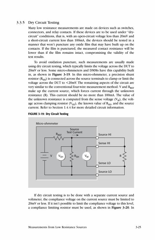
3.3.5 Dry Circuit TestingMany low resistance measurements are made on devices such as switches,connectors, and relay contacts. If these devices are to be used under “dry-circuit” conditions, that is, with an open-circuit voltage less than 20mV anda short-circuit current less than 100mA, the devices should be tested in amanner that won’t puncture any oxide film that may have built up on thecontacts. If the film is punctured, the measured contact resistance will belower than if the film remains intact, compromising the validity of the test results.
To avoid oxidation puncture, such measurements are usually madeusing dry circuit testing, which typically limits the voltage across the DUT to20mV or less. Some micro-ohmmeters and DMMs have this capability builtin, as shown in Figure 3-19. In this micro-ohmmeter, a precision shuntresistor (RSH) is connected across the source terminals to clamp or limit thevoltage across the DUT to <20mV. The remaining aspects of the circuit arevery similar to the conventional four-wire measurement method: V and RREFmake up the current source, which forces current through the unknownresistance (R). This current should be no more than 100mA. The value ofthe unknown resistance is computed from the sense voltage (VM), the volt-age across clamping resistor (VSH), the known value of RSH, and the sourcecurrent. Refer to Section 1.4.4 for more detailed circuit information.
If dry circuit testing is to be done with a separate current source andvoltmeter, the compliance voltage on the current source must be limited to20mV or less. If it isn’t possible to limit the compliance voltage to this level,a compliance limiting resistor must be used, as shown in Figure 3-20. In
Measurements from Low Resistance Sources 3-25
Micro-ohmmeter
VSHV RSH VM
RREF
Source LO
Sense LO
Sense HI
Source HI
R
SourceTest Current
FIGURE 3-19: Dry Circuit Testing
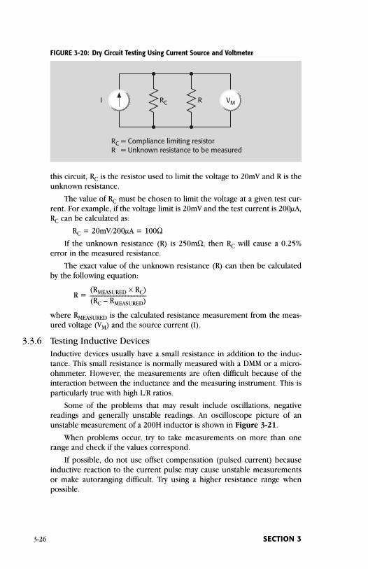
this circuit, RC is the resistor used to limit the voltage to 20mV and R is theunknown resistance.
The value of RC must be chosen to limit the voltage at a given test cur-rent. For example, if the voltage limit is 20mV and the test current is 200µA,RC can be calculated as:
RC = 20mV/200µA = 100ΩIf the unknown resistance (R) is 250mΩ, then RC will cause a 0.25%
error in the measured resistance.
The exact value of the unknown resistance (R) can then be calculatedby the following equation:
(RMEASURED × RC)R = ___________________
(RC – RMEASURED)
where RMEASURED is the calculated resistance measurement from the meas-ured voltage (VM) and the source current (I).
3.3.6 Testing Inductive DevicesInductive devices usually have a small resistance in addition to the induc-tance. This small resistance is normally measured with a DMM or a micro-ohmmeter. However, the measurements are often difficult because of theinteraction between the inductance and the measuring instrument. This isparticularly true with high L/R ratios.
Some of the problems that may result include oscillations, negativereadings and generally unstable readings. An oscilloscope picture of anunstable measurement of a 200H inductor is shown in Figure 3-21.
When problems occur, try to take measurements on more than onerange and check if the values correspond.
If possible, do not use offset compensation (pulsed current) becauseinductive reaction to the current pulse may cause unstable measurementsor make autoranging difficult. Try using a higher resistance range whenpossible.
3-26 SECTION 3
RC RI VM
RC = Compliance limiting resistorR = Unknown resistance to be measured
FIGURE 3-20: Dry Circuit Testing Using Current Source and Voltmeter
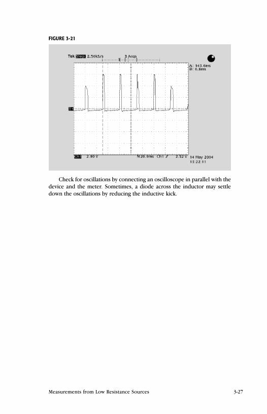
Check for oscillations by connecting an oscilloscope in parallel with thedevice and the meter. Sometimes, a diode across the inductor may settledown the oscillations by reducing the inductive kick.
Measurements from Low Resistance Sources 3-27
FIGURE 3-21
S E C T I O N 4
Applications
4.1 Introduction The applications for today’s low-level measurement instruments are nolonger limited to the calibration department or R&D lab. Low-level instru-ments have proven invaluable in many other areas, including productdesign, device characterization, quality assurance, and production test. Thissection offers insights into this growing range of applications and the mostappropriate instruments and test techniques to solve specific test and meas-urement challenges.
Section 4 covers a variety of low-level measurement applications:
4.2 Applications for Measuring Voltage from High Resistance Sources:Capacitor dielectric absorption and electrochemical measurements.
4.3 Low Current Measurement Applications: Capacitor leakage measure-ments, low current semiconductor measurements, light measurementswith photomultiplier tubes, and ion beam measurements.
4.4 High Resistance Measurement Applications: Surface insulation resist-ance testing of printed circuit boards, resistivity measurements of insu-lating materials, resistivity measurements of semiconductors, and volt-age coefficient testing of high ohmic value resistors.
4.5 Charge Measurement Applications: Capacitance measurements, staticcharge measurements using a Faraday cup.
4.6 Low Voltage Measurement Applications: Standard cell comparisons,high resolution temperature measurements, and microcalorimetry.
4.7 Low Resistance Measurement Applications: Contact resistance, super-conductor resistance measurements, and resistivity measurements ofconductive materials.
4.2 Applications for Measuring Voltage fromHigh Resistance Sources Electrometer voltmeters and voltage measurements on high resistancesources were described in Sections 1 and 2 respectively. In particular,Section 2.2 discussed error sources and ways to minimize their effects.Voltage measurements on high impedance sources include applicationssuch as capacitor dielectric absorption and some electrochemical experi-ments, including pH measurements and other ion-selective electrodes.
4.2.1 Capacitor Dielectric Absorption
Overview
Dielectric absorption occurs when randomly oriented permanent dipoles ofmolecules within a dielectric are aligned by an applied electric field. After acapacitor is disconnected from a discharge circuit, a residual charge remainson the capacitor, so a voltage is re-established across the capacitorterminals.
4-2 SECTION 4
For timing and integrating applications, dielectric absorption (or aresidual capacitor voltage) can seriously degrade the accuracy of the circuit.Thus, a capacitor’s dielectric absorption must be known and compensatedfor in circuits where capacitance tolerance is a significant factor in circuitaccuracy.
Dielectric absorption can be expressed as a percentage of a residualvoltage as compared to a charging voltage. This percentage is determined byfirst charging the capacitor to the rated voltage for a specified time interval,then discharging it for a second time interval. Finally, the capacitor is open-circuited and, after a third time interval, the residual voltage across thecapacitor is measured.
Using a Source-Measure Unit to Determine Dielectric Absorption
Residual capacitor voltage can be measured with a source-measure unit(SMU), which must source voltage and then measure voltage with a highinput impedance. Dielectric absorption is calculated from the residual volt-age value, as described in the previous paragraph. Figure 4-1 illustrates thebasic circuit configuration using a Model 6430 Sub-Femtoamp RemoteSourceMeter® instrument or other high impedance SMU, as well as a volt-age timing diagram.
The “soak” voltage is applied across the capacitor for the required soaktime (t1). Next, the SMU is programmed to output 0V with a compliance of100mA for the specified discharge interval (t2). Finally, the SMU is pro-grammed to output a current of zero on as low a current range as possiblewhile simultaneously measuring voltage. The lower the current sourcerange, the higher the input resistance will be on the SMU voltmeter. Theresidual voltage is measured after the prescribed time period (t3). Thedielectric absorption is then determined from the residual voltage:
Residual VoltageDielectric Absorption = __________________ × 100%
Soak Voltage
Using an Electrometer to Determine Dielectric Absorption
An electrometer voltmeter is particularly useful for measuring dielectricabsorption because, like an SMU, it draws virtually no charge from thecapacitor during the measurement, nor does it put charge on the capacitorbeing measured.
Figure 4-2 illustrates the basic circuit that uses an electrometer todetermine dielectric absorption. This application employs a Model 6517AElectrometer, which can supply the test voltage and measure the residualvoltage.
Initially, the capacitor (CX) is charged through R1 for the required soaktime (typically one or two minutes). Next, the voltage source is turned off;S1 is opened and S2 is closed, discharging the capacitor through R2 for therequired discharge time. Next, S2 is opened and the capacitor must remain
Applications 4-3
4-4 SECTION 4
CX
Output HI
Output LO
Capacitorunder test
b. Equivalent Circuit
V
Model 6430 or otherhigh impedance SMU
CX
Output HI
Output LO Capacitorunder test
a. Connections
Soak Recovery
Discharge
c. Voltage Waveform
Time
V
t1 t2 t3
SMU
V
FIGURE 4-1: Using an SMU to Measure Residual Voltage
undisturbed for the specified recovery time, at the end of which the elec-trometer voltmeter is used to measure the residual voltage. The dielectricabsorption is then calculated using the equation given previously.
4.2.2 Electrochemical Measurements Overview
To ensure the accuracy of measurements when determining the potentialsof electrochemical electrodes or cells, these measurements must be madewithout drawing appreciable current from the cells. Otherwise, the currentdrawn from the cell electrodes will cause a voltage drop across the internalresistance of the electrode and may polarize the cell. Therefore, a voltmeterwith high input resistance, such as an electrometer, is required.
Electrometers are commonly used for pH measurements and other ion-selective electrodes to determine a specific ionic concentration. They arealso often used for measuring liquid conductivity. This section discusses anumber of measurement fundamentals related to these applications. Keepin mind that these measurements typically require close temperature regu-lation.
Measurements with Ion-Selective Electrodes
These measurements are particularly useful where continuous measure-ments of ionic activity are needed. Such monitoring is important to preventloss of valuable material or to detect possible pollutants in the effluentsfrom industrial processes.
The cell potential of an ion-selective electrode varies directly with thelogarithm of ionic activity. At room temperature, the potential of most ion-selective electrodes will change about 57mV when the activity of an equiva-
Applications 4-5
FIGURE 4-2: Using an Electrometer to Measure Dielectric Absorption
Model 6517AElectrometer/Voltage Source
S1
R1
R2
S2
CX
HI
LO
Electrometer Input
HI
LO
Voltage Source Output
lent ion is changed by a factor of ten. This log response enables constantprecision over dynamic ranges of ionic activity of up to eight orders of mag-nitude. Figure 4-3 shows a typical circuit. Note that the ion-selective elec-trode usually has higher impedance than the reference electrode andshould be connected to the HI terminal of the electrometer input withshielded cable. The shield can be driven by the Guard (Preamp) Output toimprove the response speed. With the Model 6517A or Model 6514 elec-trometers, this can be done by either an external connection to the preampoutput (as shown) or using the volts guard function on the front panel.
pH Measurements
Any pH electrode system (Figure 4-4) can be seen as a large resistor (from10MΩ to 1GΩ) in series with a voltage source. This resistance is the sum ofthe ion-selective electrode wall (typically glass) and the electrolyte, whichhas low mobility. The potential in this system cannot be measured with anordinary DMM.
FIGURE 4-4: pH Electrode System
Glass electrode
Reference electrode
Electrolyte
Model 6514Electrometer
HI
LO
4-6 SECTION 4
Model 6514 or6517A Electrometer
Ion-selectiveElectrode
ReferenceElectrode
TestSolution
Shielded Cable
HI
LO
Guard Output usedto drive shield
FIGURE 4-3: Ion-Selective Electrode Measurements
If current flows, the electrodes will become polarized. Therefore, theelectrode potential should be measured with an electrometer, which drawsnegligible current from the electrodes. The electrometer should not bezero-checked while connected to the glass electrode; the instrument’s nor-mally near-infinite input resistance drops to 10MΩ in zero check and theresulting current flow may polarize the electrodes.
If the approximate pH to be measured is known, the electrodes shouldbe standardized, using two values of buffer solutions to calibrate the systemat each end of the desired pH scale. This step is necessary to obtain the bestaccuracy. For example, to measure from 6.5pH (29.6mV at 25°C) to 1pH(355mV at 25°C), it is advisable to use one buffer solution with a pH of sixand another with a pH of one.
When placed in the buffer solution, the voltage reading from the elec-trodes may differ from the theoretical value by several hundred microvolts.The voltage is also highly temperature dependent. For a given cell and tem-perature, the pH-to-voltage relationship is linear. For example, the theoret-ical voltage with a pH of 4.0 is 177.5mV at 25°C, assuming the calomel cellis used as the reference electrode. Other reference electrodes, such as thesilver/silver chloride cell, will give a slightly different voltage. The referenceelectrode doesn’t change with pH, so its contribution to the measurementcan be corrected for by measuring known buffer solutions. The electrodevoltages measured by the electrometer may be converted to pH values byusing appropriate conversion data. Figure 4-5 is a typical plot of millivoltdifference versus pH value.
FIGURE 4-5: Electrode Output Voltage at Various pH Values
14
12
10
8
6
4
2
0–400 –200 0 200 400
mV
pH
T =25°C
T–
T
T +T
Applications 4-7
Conductivity Cells
Measuring the electrical conductivity of many chemical solutions is difficultif the ionic concentration is very low. In these instances, an electrometervoltmeter with a current source can be used to make this measurement;Figure 4-6 shows a typical configuration.
FIGURE 4-6: Conductivity Cell Measurements
The conductivity of a solution is sensitive to the presence of impurities,so its value is meant to be more an index of impurity than a characteristicconstant. Therefore, high accuracy is unnecessary and the test equipmentneed not be elaborate.
As with pH measurements, the current should be kept as low as possi-ble. Its polarity can be alternated to avoid electrode polarization.
The electrodes of the cell must be rigidly mounted to prevent vibrationand motion from creating noise and pickup. Additionally, shielding theleads to the electrodes helps reduce interference.
Each cell arrangement has a particular constant, which is a function ofthe volume of the conducting solution between the electrodes. Electrome-ters can be very useful where electrode areas are very small and solutionconductivities are very low. Temperature control is essential to making reli-able measurements.
Conductivity is computed from the known value of current (I), the volt-age reading (V), and the area and spacing between the electrodes:
I Lσ = ___ · ___
V A
where: σ = conductivity (Siemens/cm)
A = surface area of the electrodes (cm2)
L = distance between the electrodes (cm)
Model 6514Electrometer
Electrodeof area “A”
SolutionL
CurrentSource
LO
HI
LO
HI
4-8 SECTION 4
4.3 Low Current Measurement Applications Electrometer ammeters and picoammeters and methods of making low cur-rent measurements were described in Sections 1 and 2 respectively. In par-ticular, Section 2.3 discussed a number of error sources that can seriouslyaffect measurement accuracy. Low current measurement applicationsinclude capacitor leakage, low current semiconductor, light, and ion beammeasurements.
4.3.1 Capacitor Leakage Measurements Overview
Capacitors are essential components of virtually every type of electronicequipment. They are widely used for bypassing, coupling, filtering, and tun-ing electronic circuits. However, to be useful, they must be characterized forcapacitance value, voltage rating, temperature coefficient, and leakageresistance. The capacitor manufacturer performs these tests; end users mayalso perform them.
This application focuses on the measurement of leakage resistanceusing either a Model 6487 Picoammeter/Source or a Model 6517A Electrom-eter. This leakage resistance may be referred to as “IR” (Insulation Resist-ance) and is expressed in megohm-microfarads (the resistance may be com-puted by dividing the “IR” value by the capacitance). In other cases, leakagemay be expressed as a leakage current at a given voltage, usually the oper-ating voltage.
Description of Test Method
Capacitor leakage is measured by applying a fixed voltage to the capacitorunder test and measuring the resulting current. The leakage current willdecay exponentially with time, so it’s usually necessary to apply the voltagefor a known period (the “soak” time) before measuring the current.
Figure 4-7 depicts a general circuit for testing capacitor leakage. Here,the voltage is placed across the capacitor (CX) for the soak period, then theammeter measures the current after this period has elapsed. The resistor(R), which is in series with the capacitor, is an important component in thistest system. The resistor has two functions:
1. The resistor limits the current in case the capacitor becomes shorted.
2. As discussed in Section 2.3.2, the decreasing reactance of the capacitorwith increasing frequency will increase the gain of the feedback amme-ter. The resistor limits this increase in gain to a finite value. A reason-able value is one that results in an RC product from 0.5 to 2 seconds.
Even better performance will result if a forward-biased diode (D) isincluded in the circuit, as shown in Figure 4-8. The diode acts like a vari-able resistance, low when the charging current to the capacitor is high, thenincreasing in value as the current decreases with time. The series resistorcan be much smaller since it is only needed to prevent overload of the volt-
Applications 4-9
age source and damage to the diode if the capacitor becomes short-circuit-ed. The diode should be a small signal diode, such as 1N914 or 1N3595, andmust be in a light-tight enclosure. For dual-polarity tests, use two diodesback-to-back in parallel.
Test Circuit
For statistical purposes, a quantity of capacitors is often tested to produceuseful data. Obviously, it is impractical to perform these tests manually, sosome sort of automated test system is required. Figure 4-9 illustrates sucha system, which employs a Model 6487 Picoammeter/Voltage Source, Model7158 Low Current Scanner Cards, and Model 7169A Form C Switch Cards.The cards must be installed in a switching mainframe, such as a Model 7002.A computer controls the instruments to perform the tests automatically.
In this test system, a single instrument, the Model 6487 Picoammeter/Source, provides both the voltage sourcing and low current measurementfunctions. This instrument is particularly useful for this application becauseit can display either resistance or leakage current and will source up to 500V
4-10 SECTION 4
Picoammeter
CXV
S R
Voltage Source
CapacitorUnder Test
HI
LO
IM
FIGURE 4-7: Simple Capacitor Leakage Test Circuit
D
Picoammeter
CX
V
S R
Voltage Source
HI
LO
IM
FIGURE 4-8: Capacitor Leakage Test Circuit with Diode
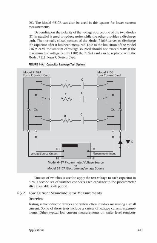
DC. The Model 6517A can also be used in this system for lower currentmeasurements.
Depending on the polarity of the voltage source, one of the two diodes(D) in parallel is used to reduce noise while the other provides a dischargepath. The normally closed contact of the Model 7169A serves to dischargethe capacitor after it has been measured. Due to the limitation of the Model7169A card, the amount of voltage sourced should not exceed 500V. If themaximum test voltage is only 110V, the 7169A card can be replaced with theModel 7111 Form C Switch Card.
FIGURE 4-9: Capacitor Leakage Test System
One set of switches is used to apply the test voltage to each capacitor inturn; a second set of switches connects each capacitor to the picoammeterafter a suitable soak period.
4.3.2 Low Current Semiconductor Measurements Overview
Testing semiconductor devices and wafers often involves measuring a smallcurrent. Some of these tests include a variety of leakage current measure-ments. Other typical low current measurements on wafer level semicon-
Model 6487 Picoammeter/Voltage Sourceor
Model 6517A Electrometer/Voltage Source
R
Model 7169AForm C Switch Card
Model 7158Low Current Card
LO
HI
Voltage Source Output
LO
HI
Picoammeter Input
R
R
C
C
C
D
Applications 4-11
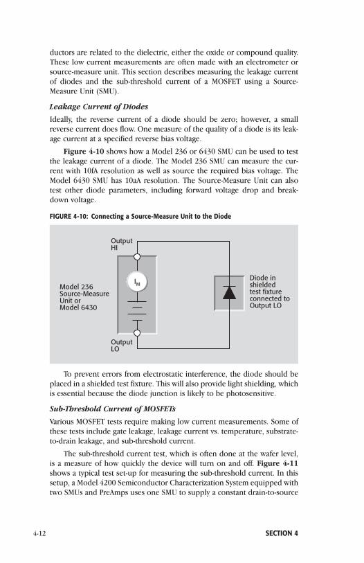
ductors are related to the dielectric, either the oxide or compound quality.These low current measurements are often made with an electrometer orsource-measure unit. This section describes measuring the leakage currentof diodes and the sub-threshold current of a MOSFET using a Source-Measure Unit (SMU).
Leakage Current of Diodes
Ideally, the reverse current of a diode should be zero; however, a smallreverse current does flow. One measure of the quality of a diode is its leak-age current at a specified reverse bias voltage.
Figure 4-10 shows how a Model 236 or 6430 SMU can be used to testthe leakage current of a diode. The Model 236 SMU can measure the cur-rent with 10fA resolution as well as source the required bias voltage. TheModel 6430 SMU has 10aA resolution. The Source-Measure Unit can alsotest other diode parameters, including forward voltage drop and break-down voltage.
FIGURE 4-10: Connecting a Source-Measure Unit to the Diode
To prevent errors from electrostatic interference, the diode should beplaced in a shielded test fixture. This will also provide light shielding, whichis essential because the diode junction is likely to be photosensitive.
Sub-Threshold Current of MOSFETs
Various MOSFET tests require making low current measurements. Some ofthese tests include gate leakage, leakage current vs. temperature, substrate-to-drain leakage, and sub-threshold current.
The sub-threshold current test, which is often done at the wafer level,is a measure of how quickly the device will turn on and off. Figure 4-11shows a typical test set-up for measuring the sub-threshold current. In thissetup, a Model 4200 Semiconductor Characterization System equipped withtwo SMUs and PreAmps uses one SMU to supply a constant drain-to-source
IM
OutputHI
OutputLO
Diode inshieldedtest fixtureconnected toOutput LO
Model 236Source-MeasureUnit orModel 6430
4-12 SECTION 4
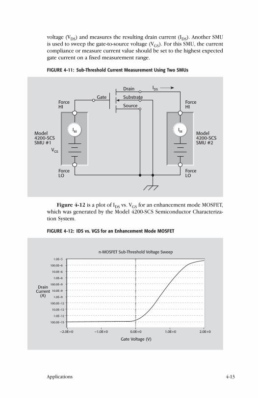
voltage (VDS) and measures the resulting drain current (IDS). Another SMUis used to sweep the gate-to-source voltage (VGS). For this SMU, the currentcompliance or measure current value should be set to the highest expectedgate current on a fixed measurement range.
FIGURE 4-11: Sub-Threshold Current Measurement Using Two SMUs
Figure 4-12 is a plot of IDS vs. VGS for an enhancement mode MOSFET,which was generated by the Model 4200-SCS Semiconductor Characteriza-tion System.
FIGURE 4-12: IDS vs. VGS for an Enhancement Mode MOSFET
1.0E–3
100.0E–6
10.0E–6
1.0E–6
100.0E–9
10.0E–9
1.0E–9
100.0E–12
10.0E–12
1.0E–12
100.0E–15
n-MOSFET Sub-Threshold Voltage Sweep
DrainCurrent
(A)
Gate Voltage (V)
–2.0E+0 –1.0E+0 0.0E+0 1.0E+0 2.0E+0
Drain
Substrate
Source
Gate
IM
ForceHI
ForceLO
Model4200-SCSSMU #1
IM
ForceHI
ForceLO
Model4200-SCSSMU #2
VGS
IDS
Applications 4-13

4.3.3 Light Measurements with Photomultiplier Tubes
Overview
Applications such as measuring light with a photomultiplier tube generallyrequire the use of a picoammeter due to the low current levels involved.
A photomultiplier tube (PMT) is a device for converting light to electri-cal current. The tube consists of a light-sensitive cathode that emits elec-trons in proportion to the photons striking it. These electrons are thenaccelerated to the next stage, where they impinge and cause the emission ofthree to six secondary electrons. The process continues through six to four-teen stages (called “dynodes”), depending on tube type. Overall gains ofone million or more are commonly attained.
Detailed Operation
Electrons are accelerated by making the voltage of each successive dynodeof the tube more positive than the previous one. The easiest way to accom-plish this is to apply a potential across the entire tube and tap the dynodevoltages off a voltage divider, as shown in Figure 4-13.
FIGURE 4-13: Voltage Supply for Photomultiplier Tube
The voltages that should be applied to each dynode are a function ofPMT design and are specified for each tube type.
The total resistance of the dynode resistors should be such that the cur-rent flowing through the series resistance is at least 100 times the expectedanode current of the tube:
Voltage, Anode-to-CathodeRT = ______________________________
100 × Anode Current
Most photomultiplier tubes require anode-to-cathode potentials offrom 1000 to 3000V. The anode is the readout point, so it is usually operat-ed at near-ground potential and the cathode at a high negative potential.
R1
Photomultiplier Tube
Cathode Anode
Dynodes
R2 R3 R4 R5 R6
– +
4-14 SECTION 4
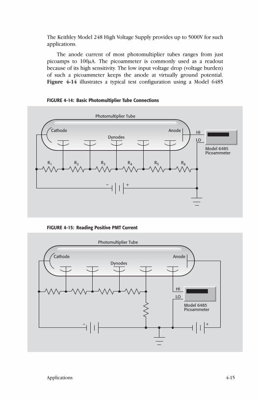
The Keithley Model 248 High Voltage Supply provides up to 5000V for suchapplications.
The anode current of most photomultiplier tubes ranges from justpicoamps to 100µA. The picoammeter is commonly used as a readoutbecause of its high sensitivity. The low input voltage drop (voltage burden)of such a picoammeter keeps the anode at virtually ground potential.Figure 4-14 illustrates a typical test configuration using a Model 6485
Applications 4-15
– +
R1
Photomultiplier Tube
Cathode Anode
Dynodes
R2 R3 R4 R5 R6
Model 6485Picoammeter
HI
LO
FIGURE 4-14: Basic Photomultiplier Tube Connections
– +
Photomultiplier Tube
Cathode Anode
Dynodes
Model 6485Picoammeter
HI
LO
FIGURE 4-15: Reading Positive PMT Current
Picoammeter. If the PMT requires no more than 1000V, the 6517AElectrometer/Source would provide a convenient solution because it canmeasure the current as well as supply the voltage.
With this connection method, the picoammeter reads a negative cur-rent. Occasionally, the current must be measured as a positive value. In suchcases, a simple re-arrangement and an additional power supply permit read-ing positive current. The configuration for measuring positive PMT currentis shown in Figure 4-15. The picoammeter reads the current at the last dyn-ode, which is equal to the anode current minus the current flowing to theprevious dynode. In effect, a slight amount of PMT gain is sacrificed to makethe measurement.
A PMT usually has a small amount of current flowing even when thecathode is not illuminated. This phenomenon is known as “dark current,”and is insignificant in most measurements. In other cases, it can either besubtracted from the reading by using the REL (zero) feature or simply can-celed out by using built-in zero suppression if the instrument has thisfeature.
4.3.4 Ion Beam Measurements Overview
Ion beams are used in a variety of applications, such as with mass spec-trometers and ion implanters. Ion beam current is usually very small (<µA),so an electrometer or picoammeter is needed to make this measurement.This section describes how to make these measurements with a Model 6485Picoammeter and a Model 6487 Picoammeter/Voltage Source. An electrom-eter can be substituted for greater current sensitivity.
Test Method
If the source of ions is biased off ground, then the ion collector will mostlikely be at ground potential. If this is the case, a simple coaxial vacuumfeedthrough can be used to make connections from the collector to thepicoammeter. Figure 4-16 shows a Model 6485 Picoammeter measuring thecurrent from the ion collector, which is operating at ground potential.
However, if the source of ions is at ground potential, then the ion col-lector must be biased off ground. The Model 6485 Picoammeter can float offround by only 42V. Therefore, a picoammeter such as the Model 6487,which can float off ground up to 500V, must be used. Figure 4-17 is anexample of the Model 6487 biased off ground and measuring an ion beam.The HI terminal of the picoammeter is connected to the ion collector via atriax vacuum feedthrough. The LO terminal of the picoammeter is biased offground by the voltage source. For safety reasons, a triaxial vacuumfeedthrough should be used if the bias voltage is more than 42V. The Model6487 can supply up to 500V of bias.
If a triaxial vacuum feedthrough is unavailable, a metal safety shieldshould be built around the isolated BNC connection (Figure 4-18). The
4-16 SECTION 4
metal safety shield is connected to ground. Floating input signals are dis-cussed in detail in Section 2.6.8.
If the bias voltage is less than 42V off ground, the isolated BNC vacuumfeedthrough will not need a safety shield.
After the connections are made, verify the system is working properly byturning the bias voltage on and taking a current measurement with no ionbeam current. If there is significant current compared to the current to bemeasured, there must be a stray leakage path, which should be corrected.
Often, the beam current is plotted as a function of time. This can bedone by using either the analog output of the picoammeter or the IEEE-488
Applications 4-17
Ion Beam
BNC Vacuum Feedthrough(grounded to vacuum chamber wall)
HI
LO
Model 6485Picoammeter IM
FIGURE 4-16: Ion Collector with Grounded BNC Receptacle
Ion Beam
Triax VacuumFeedthrough
Guard(if needed)
HI
LO
Model 6487Picoammeter/Source
IM
FIGURE 4-17: Ion Collector with Triax Receptacle
bus or RS-232 output to collect readings, then plotting them with a graphi-cal programming software package (such as ExceLINX) or a spreadsheet.
4.3.5 Avalanche Photodiode Reverse Bias Current Measurements
Overview
An avalanche photodiode (APD) is a high sensitivity, high speed photodiodethat has an internal gain mechanism activated by applying a reverse voltage.The gain of the APD can be controlled by the magnitude of the reverse biasvoltage. A larger reverse bias voltage results in a larger gain. APDs are oper-ated with an electric field strength such that an avalanche multiplication ofphotocurrent occurs similar to a chain reaction. APDs are used in a varietyof applications requiring high sensitivity to light such as fiberoptic commu-nications and scintillation detectors.
Common electrical measurements of APDs typically include the break-down voltage, responsivity, and reversed bias current measurements. Themaximum current rating for a typical APD is 10–4 to 10–2A, while the darkcurrent can be as low as the 10–12 to 10–13A range. The maximum reversebias voltage will vary, depending on the material of the APD, but can be upto 100V for InGaAs APDs or up to 500V for Si devices.
Test Description
Measuring the reverse bias current of an APD requires an instrument thatcan measure current over a wide range as well as output a voltage sweep.Because of these requirements, instruments such as the Model 6487Picoammeter/Voltage Source or the Model 6430 Sub-Femtoamp Source-Meter instrument are ideal for these measurements.
4-18 SECTION 4
Ion Beam
Floating BNCVacuum
Feedthrough
Guard(if needed)
Grounded metal shield to protectagainst touching the BNC connector
HI
LO
Model 6487Picoammeter/Source
IM
FIGURE 4-18: Ion Collector with BNC Receptacle
Figure 4-19 shows a Model 6430 connected to a photodiode. The pho-todiode is placed in an electrically shielded dark box. To shield the sensitivecurrent measurements from electrostatic interference, connect the box tothe LO terminal of the Model 6430.
FIGURE 4-19: APD Connected to a Model 6430 Sub-Femtoamp Remote SourceMeterInstrument
Figure 4-20 shows a current vs. reverse voltage sweep of an InGaAsAPD, generated by the Model 6430 SourceMeter. Note the wide range ofcurrent measurements. The avalanche region becomes more pronouncedwith increasing light. The breakdown voltage will cause the current to flowfreely since electron-hole pairs will form without the need for light strikingthe diode to generate current.
FIGURE 4-20: Current vs. Reverse Voltage Sweep of an InGaAs APD
IM
HI
LO
APDModel 6430SourceMeterInstrument
ShieldedBox
Applications 4-19
1.0E–4
1.0E–5
1.0E–6
1.0E–7
1.0E–8
1.0E–9
1.0E–10
1.0E–11
1.0E–12
Current(A)
Voltage (V)
0 10 20 30 40 50 60
Avalanche
Breakdown
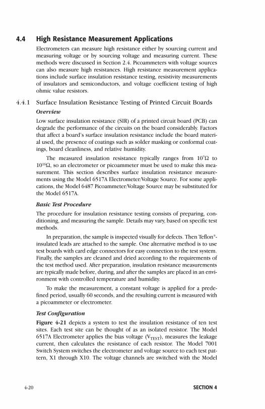
4.4 High Resistance Measurement ApplicationsElectrometers can measure high resistance either by sourcing current andmeasuring voltage or by sourcing voltage and measuring current. Thesemethods were discussed in Section 2.4. Picoammeters with voltage sourcescan also measure high resistances. High resistance measurement applica-tions include surface insulation resistance testing, resistivity measurementsof insulators and semiconductors, and voltage coefficient testing of highohmic value resistors.
4.4.1 Surface Insulation Resistance Testing of Printed Circuit Boards Overview
Low surface insulation resistance (SIR) of a printed circuit board (PCB) candegrade the performance of the circuits on the board considerably. Factorsthat affect a board’s surface insulation resistance include the board materi-al used, the presence of coatings such as solder masking or conformal coat-ings, board cleanliness, and relative humidity.
The measured insulation resistance typically ranges from 107Ω to1016Ω, so an electrometer or picoammeter must be used to make this mea-surement. This section describes surface insulation resistance measure-ments using the Model 6517A Electrometer/Voltage Source. For some appli-cations, the Model 6487 Picoammeter/Voltage Source may be substituted forthe Model 6517A.
Basic Test Procedure
The procedure for insulation resistance testing consists of preparing, con-ditioning, and measuring the sample. Details may vary, based on specific testmethods.
In preparation, the sample is inspected visually for defects. Then Teflon®-insulated leads are attached to the sample. One alternative method is to usetest boards with card edge connectors for easy connection to the test system.Finally, the samples are cleaned and dried according to the requirements ofthe test method used. After preparation, insulation resistance measurementsare typically made before, during, and after the samples are placed in an envi-ronment with controlled temperature and humidity.
To make the measurement, a constant voltage is applied for a prede-fined period, usually 60 seconds, and the resulting current is measured witha picoammeter or electrometer.
Test Configuration
Figure 4-21 depicts a system to test the insulation resistance of ten testsites. Each test site can be thought of as an isolated resistor. The Model6517A Electrometer applies the bias voltage (VTEST), measures the leakagecurrent, then calculates the resistance of each resistor. The Model 7001Switch System switches the electrometer and voltage source to each test pat-tern, X1 through X10. The voltage channels are switched with the Model
4-20 SECTION 4

7111-S 40-Channel Form C Switch Card, while the current channels areswitched with the Model 7158 Low Current Scanner Card. Note that themaximum source voltage is limited to 110V when using the Model 7111-SCard.
To measure X1, Channel 1 on the 7111-S Card and Channel 1 on the7158 Card are closed. This will bias the X1 resistor and, after a specified“soak” time, the resulting current is measured. To measure the X2 resistor,Channel 1 on both the 7111-S and 7158 cards is opened, and Channel 2 onboth cards is closed. Again, the current is measured after the desired soaktime.
The resistors (RL) are current limiting resistors used to protect theswitches and electrometer from high current. These resistor values shouldbe such that the voltage drop at the maximum measured current will notaffect measurement accuracy.
Note that when a channel is opened, the corresponding resistor termi-nal is connected to circuit LO. This allows any charge across the resistanceto be discharged to circuit LO when the resistance is not being measured.
Even though the system described here measures just ten test sites, itcan be expanded easily to test more sites by adding scanner cards and sub-stituting the Model 7002 Scanner Mainframe, which can control up to tenscanner cards, for the Model 7001.
Applications 4-21
RLX10
RLX2
RLX1
VTEST
1
2
10
1
2
10
Card 1Model 7111-SForm C Switch Card
Card 2Model 7158Low Current Card
HI
LO
Model 6517AElectrometer/Voltage Source orModel 6487Picoammeter/Voltage Source
X1 through X10 are SIRTest Sites and may allbe on one PCB.
IM
FIGURE 4-21: SIR Test System to Measure Ten Test Sites

4.4.2 Resistivity Measurements of Insulating Materials Overview
Resistivity is determined by measuring resistance, then converting to surfaceor volume resistivity by taking geometric considerations into account. Theideal way to measure the resistance of an insulating material is to apply aknown potential to the sample and measure the resulting current with anelectrometer or picoammeter. To account for the sample’s geometry, elec-trodes with convenient dimensions should be used, such as Keithley’sModel 8009 Resistivity Chamber. The electrodes follow the ASTM StandardD257 entitled “DC Resistance or Conductance of Insulating Materials.” Thissection details how to make surface and volume resistivity measurementswith these test fixtures, as well as the Alternating Polarity and AlternatingVoltage techniques for measuring resistivity.
Volume Resistivity Measurements
Volume resistivity is a measure of the leakage current directly through amaterial. It is defined as the electrical resistance through a one-centimetercube of insulating material and is expressed in ohm-centimeters. Whenmeasuring the volume resistivity, the test sample is placed between twoelectrodes and a potential difference is applied between them. The result-ing current is distributed through the volume of the test sample and ismeasured using a picoammeter or electrometer. The resistivity is calculatedfrom the geometry of the electrodes and the thickness of the sample:
KV Vρ = ___ · ___
t I
where: ρ = volume resistivity (ohm-cm)
KV = test cell constant for volume resistivity based on cellgeometry (cm2)
V = applied voltage (volts)
I = measured current (amperes)
t = sample thickness (cm)
Figure 4-22 depicts a measurement configuration that complies withASTM D257 for volume resistivity measurements. In this circuit, the HI ofthe ammeter is placed on the bottom electrode and the HI of the voltagesource to the top electrode. The LO of the ammeter and the LO of thesource are connected together. The bottom outside electrode is connectedto guard (LO of the ammeter) to prevent surface leakage currents frombeing added into the measurement.
Surface Resistivity Measurements
Surface resistivity is defined as the electrical resistance of the surface of amaterial and is expressed in ohms (usually referred to as ohms per square).It is measured by placing two electrodes on the surface of the test sample,
4-22 SECTION 4
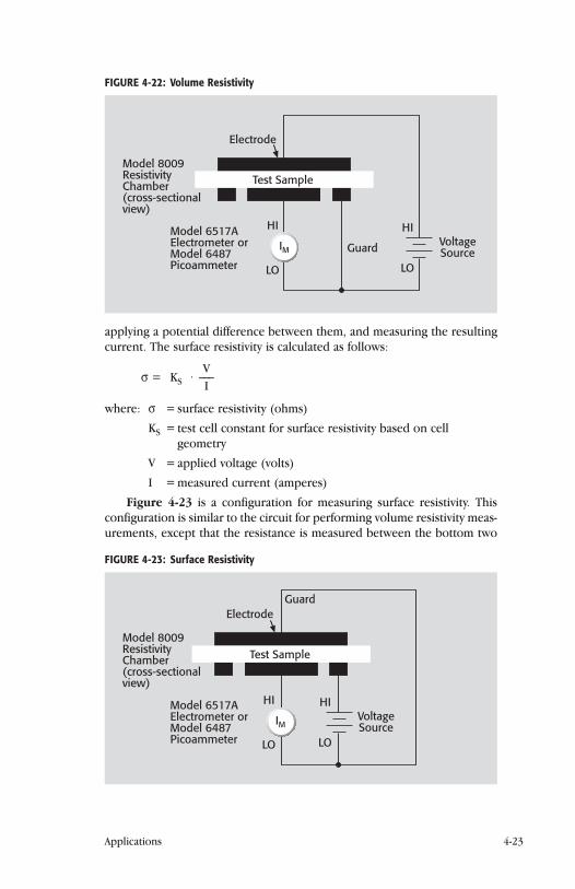
applying a potential difference between them, and measuring the resultingcurrent. The surface resistivity is calculated as follows:
Vσ = KS · ___
I
where: σ = surface resistivity (ohms)
KS = test cell constant for surface resistivity based on cellgeometry
V = applied voltage (volts)
I = measured current (amperes)
Figure 4-23 is a configuration for measuring surface resistivity. Thisconfiguration is similar to the circuit for performing volume resistivity meas-urements, except that the resistance is measured between the bottom two
Applications 4-23
Test Sample
Guard
VoltageSource
Electrode
HI
LO
HI
LO
IM
Model 8009ResistivityChamber(cross-sectionalview)
Model 6517AElectrometer orModel 6487Picoammeter
FIGURE 4-23: Surface Resistivity
Test Sample
HI
LO
Guard VoltageSource
HI
LO
Electrode
IM
Model 8009ResistivityChamber(cross-sectionalview)
Model 6517AElectrometer orModel 6487Picoammeter
FIGURE 4-22: Volume Resistivity
electrodes. Note the top electrode is guarded, so that only current flowingacross the insulator is measured by the picoammeter.
Test Parameters
Volume and surface resistivity measurements are dependent on several fac-tors. First, they are functions of the applied voltage. Sometimes, the voltagemay be varied intentionally to determine the voltage dependence of an insu-lator. The resistivity also varies as a function of the length of electrificationtime. The longer the voltage is applied, the lower the measured currentbecomes because the material continues to charge exponentially.
Humidity greatly affects the results of surface resistivity measurementsand, to a lesser degree, volume resistivity measurements, as well. Moisturewill cause the surface resistivity measurements to be lower than normal.
To make accurate comparisons between specific tests, the applied volt-age, electrification time, and environmental conditions should be kept con-stant from one test to the next.
Using the Model 8009 Resistivity Chamber
No sample preparation is necessary when using the Model 8009 ResistivityChamber. This fixture ensures a standardized electrode configuration, elim-inating the need to paint electrodes on the sample or use mercury-filledrings. The recommended sample size for using this test fixture is 2.5–4 inch-es in diameter and up to 0.125 inch thick.
Some extremely rigid samples, such as glass epoxy and ceramics,require an interface between stainless steel electrodes and the sample sur-face. The Model 8009 includes conductive rubber for the top and bottomelectrodes to enhance surface contact between the sample and the fixture.Care must be taken because the electrode area becomes the area of the con-tact medium. If it is not the same configuration and size as the electrodes,the conversion constants furnished with the system may be invalid.
The Model 8009 employs a safety interlock to prevent the high voltagefrom being applied to the electrode until the test fixture lid is closed. Thisfixture also shields the sample from electrostatic interference.
Offset Correction Techniques
When measuring materials with very high resistivity, background currentsmay cause measurement errors. Background currents may be due to chargestored in the material (dielectric absorption), static or triboelectric charge,or piezoelectric effects. Background currents can be equal to or greater thanthe current stimulated by the applied voltage. If the background current isthe same polarity as the measured current, the resultant measured currentvalue will be much higher than the true value. If the background current isthe opposite polarity, these unwanted currents could cause a reverse polar-ity current reading. That is, the current polarity is opposite the polarity ofthe applied voltage, so the calculated resistance will be negative. To counter
4-24 SECTION 4
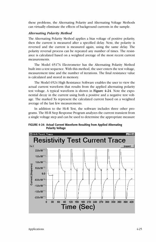
these problems, the Alternating Polarity and Alternating Voltage Methodscan virtually eliminate the effects of background currents in the sample.
Alternating Polarity Method
The Alternating Polarity Method applies a bias voltage of positive polarity,then the current is measured after a specified delay. Next, the polarity isreversed and the current is measured again, using the same delay. Thepolarity reversal process can be repeated any number of times. The resist-ance is calculated based on a weighted average of the most recent currentmeasurements.
The Model 6517A Electrometer has the Alternating Polarity Methodbuilt into a test sequence. With this method, the user enters the test voltage,measurement time and the number of iterations. The final resistance valueis calculated and stored in memory.
The Model 6524 High Resistance Software enables the user to view theactual current waveform that results from the applied alternating polaritytest voltage. A typical waveform is shown in Figure 4-24. Note the expo-nential decay in the current using both a positive and a negative test volt-age. The marked Xs represent the calculated current based on a weightedaverage of the last few measurements.
In addition to the Hi-R Test, the software includes three other pro-grams. The HI-R Step Response Program analyzes the current transient froma single voltage step and can be used to determine the appropriate measure
Applications 4-25
FIGURE 4-24: Actual Current Waveform Resulting from Applied Alternating Polarity Voltage
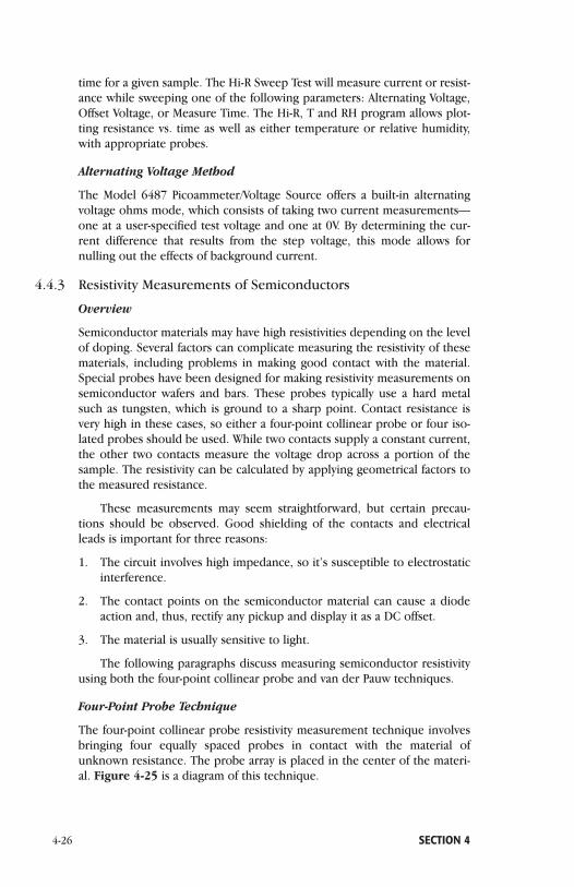
time for a given sample. The Hi-R Sweep Test will measure current or resist-ance while sweeping one of the following parameters: Alternating Voltage,Offset Voltage, or Measure Time. The Hi-R, T and RH program allows plot-ting resistance vs. time as well as either temperature or relative humidity,with appropriate probes.
Alternating Voltage Method
The Model 6487 Picoammeter/Voltage Source offers a built-in alternatingvoltage ohms mode, which consists of taking two current measurements—one at a user-specified test voltage and one at 0V. By determining the cur-rent difference that results from the step voltage, this mode allows fornulling out the effects of background current.
4.4.3 Resistivity Measurements of Semiconductors
Overview
Semiconductor materials may have high resistivities depending on the levelof doping. Several factors can complicate measuring the resistivity of thesematerials, including problems in making good contact with the material.Special probes have been designed for making resistivity measurements onsemiconductor wafers and bars. These probes typically use a hard metalsuch as tungsten, which is ground to a sharp point. Contact resistance isvery high in these cases, so either a four-point collinear probe or four iso-lated probes should be used. While two contacts supply a constant current,the other two contacts measure the voltage drop across a portion of thesample. The resistivity can be calculated by applying geometrical factors tothe measured resistance.
These measurements may seem straightforward, but certain precau-tions should be observed. Good shielding of the contacts and electricalleads is important for three reasons:
1. The circuit involves high impedance, so it’s susceptible to electrostaticinterference.
2. The contact points on the semiconductor material can cause a diodeaction and, thus, rectify any pickup and display it as a DC offset.
3. The material is usually sensitive to light.
The following paragraphs discuss measuring semiconductor resistivityusing both the four-point collinear probe and van der Pauw techniques.
Four-Point Probe Technique
The four-point collinear probe resistivity measurement technique involvesbringing four equally spaced probes in contact with the material ofunknown resistance. The probe array is placed in the center of the materi-al. Figure 4-25 is a diagram of this technique.
4-26 SECTION 4
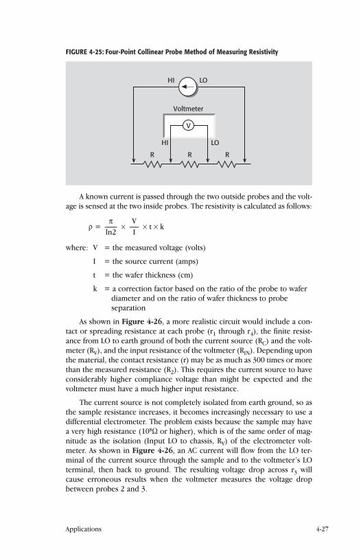
FIGURE 4-25: Four-Point Collinear Probe Method of Measuring Resistivity
A known current is passed through the two outside probes and the volt-age is sensed at the two inside probes. The resistivity is calculated as follows:
π Vρ = ____ × ___ × t × k
ln2 I
where: V = the measured voltage (volts)
I = the source current (amps)
t = the wafer thickness (cm)
k = a correction factor based on the ratio of the probe to waferdiameter and on the ratio of wafer thickness to probeseparation
As shown in Figure 4-26, a more realistic circuit would include a con-tact or spreading resistance at each probe (r1 through r4), the finite resist-ance from LO to earth ground of both the current source (RC) and the volt-meter (RV), and the input resistance of the voltmeter (RIN). Depending uponthe material, the contact resistance (r) may be as much as 300 times or morethan the measured resistance (R2). This requires the current source to haveconsiderably higher compliance voltage than might be expected and thevoltmeter must have a much higher input resistance.
The current source is not completely isolated from earth ground, so asthe sample resistance increases, it becomes increasingly necessary to use adifferential electrometer. The problem exists because the sample may havea very high resistance (108Ω or higher), which is of the same order of mag-nitude as the isolation (Input LO to chassis, RV) of the electrometer volt-meter. As shown in Figure 4-26, an AC current will flow from the LO ter-minal of the current source through the sample and to the voltmeter’s LOterminal, then back to ground. The resulting voltage drop across r3 willcause erroneous results when the voltmeter measures the voltage dropbetween probes 2 and 3.
Voltmeter
R R R
V
HI LO
HI LO
Applications 4-27

4-28 SECTION 4
R1 R2 R3
r1 r2 r3 r4
RIN
1 2 3 4
AC
AC
RV
RC
Common-ModeCurrent
LO
Voltmeter
V
HI
LOHI
Current Source
I
FIGURE 4-26: Realistic Circuit of the Four-Point Collinear Probe Method
R1 R2 R3
×1Buffer
×1Buffer
r1 r2 r3 r4
1 2 3 4
HI LO
Voltmeter
V
HI LO
HI LOLO HI
FIGURE 4-27: Making Differential Four-Point Probe Measurements
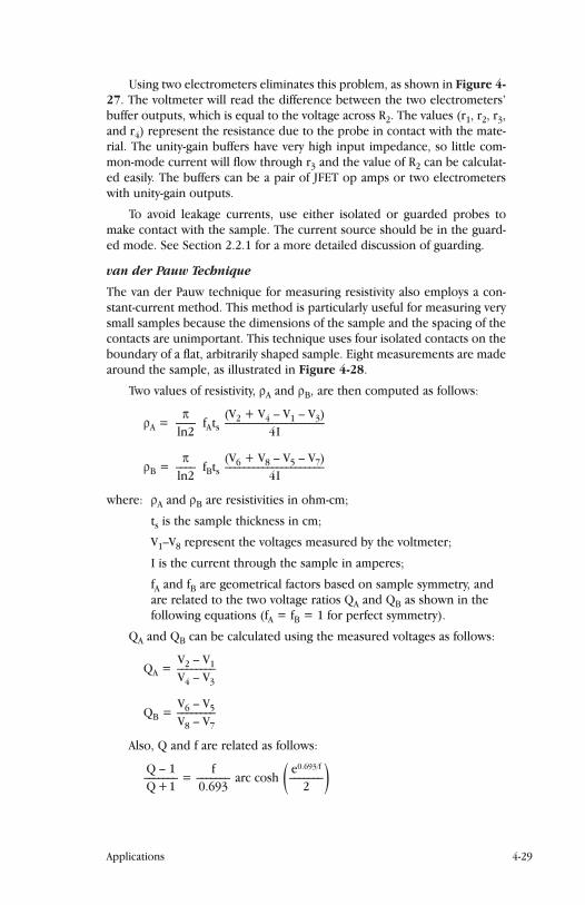
Using two electrometers eliminates this problem, as shown in Figure 4-27. The voltmeter will read the difference between the two electrometers’buffer outputs, which is equal to the voltage across R2. The values (r1, r2, r3,and r4) represent the resistance due to the probe in contact with the mate-rial. The unity-gain buffers have very high input impedance, so little com-mon-mode current will flow through r3 and the value of R2 can be calculat-ed easily. The buffers can be a pair of JFET op amps or two electrometerswith unity-gain outputs.
To avoid leakage currents, use either isolated or guarded probes tomake contact with the sample. The current source should be in the guard-ed mode. See Section 2.2.1 for a more detailed discussion of guarding.
van der Pauw Technique
The van der Pauw technique for measuring resistivity also employs a con-stant-current method. This method is particularly useful for measuring verysmall samples because the dimensions of the sample and the spacing of thecontacts are unimportant. This technique uses four isolated contacts on theboundary of a flat, arbitrarily shaped sample. Eight measurements are madearound the sample, as illustrated in Figure 4-28.
Two values of resistivity, ρA and ρB, are then computed as follows:
π (V2 + V4 – V1 – V3)ρA = ____ fAts
_____________________ln2 4I
π (V6 + V8 – V5 – V7)ρB = ____ fBts
_____________________ln2 4I
where: ρA and ρB are resistivities in ohm-cm;
ts is the sample thickness in cm;
V1–V8 represent the voltages measured by the voltmeter;
I is the current through the sample in amperes;
fA and fB are geometrical factors based on sample symmetry, andare related to the two voltage ratios QA and QB as shown in thefollowing equations (fA = fB = 1 for perfect symmetry).
QA and QB can be calculated using the measured voltages as follows:
V2 – V1QA = ________V4 – V3
V6 – V5QB = ________V8 – V7
Also, Q and f are related as follows:
Q – 1 f e0.693/f_______ = _______ arc cosh _______Q + 1 0.693 ( 2 )
Applications 4-29

4-30 SECTION 4
V1
1 2
4 3
V2
1 2
4 3
V4
1 2
4 3
V3
1 2
4 3
V5
1 2
4 3
V6
1 2
4 3
V8
1 2
4 3
V7
1 2
4 3
FIGURE 4-28: van der Pauw Resistivity Measurement Conventions
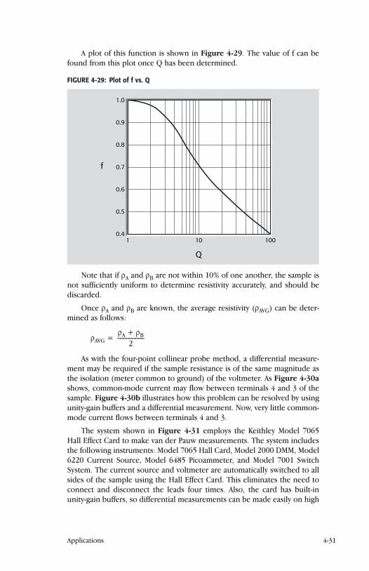
A plot of this function is shown in Figure 4-29. The value of f can befound from this plot once Q has been determined.
FIGURE 4-29: Plot of f vs. Q
Note that if ρA and ρB are not within 10% of one another, the sample isnot sufficiently uniform to determine resistivity accurately, and should bediscarded.
Once ρA and ρB are known, the average resistivity (ρAVG) can be deter-mined as follows:
ρA + ρBρAVG = _________2
As with the four-point collinear probe method, a differential measure-ment may be required if the sample resistance is of the same magnitude asthe isolation (meter common to ground) of the voltmeter. As Figure 4-30ashows, common-mode current may flow between terminals 4 and 3 of thesample. Figure 4-30b illustrates how this problem can be resolved by usingunity-gain buffers and a differential measurement. Now, very little common-mode current flows between terminals 4 and 3.
The system shown in Figure 4-31 employs the Keithley Model 7065Hall Effect Card to make van der Pauw measurements. The system includesthe following instruments: Model 7065 Hall Card, Model 2000 DMM, Model6220 Current Source, Model 6485 Picoammeter, and Model 7001 SwitchSystem. The current source and voltmeter are automatically switched to allsides of the sample using the Hall Effect Card. This eliminates the need toconnect and disconnect the leads four times. Also, the card has built-inunity-gain buffers, so differential measurements can be made easily on high
101 1000.4
0.5
0.6
0.7
0.8
0.9
1.0
Q
f
Applications 4-31
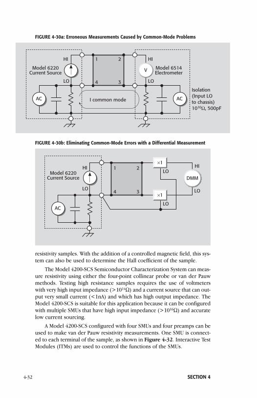
resistivity samples. With the addition of a controlled magnetic field, this sys-tem can also be used to determine the Hall coefficient of the sample.
The Model 4200-SCS Semiconductor Characterization System can meas-ure resistivity using either the four-point collinear probe or van der Pauwmethods. Testing high resistance samples requires the use of voltmeterswith very high input impedance (>1014Ω) and a current source that can out-put very small current (<1nA) and which has high output impedance. TheModel 4200-SCS is suitable for this application because it can be configuredwith multiple SMUs that have high input impedance (>1016Ω) and accuratelow current sourcing.
A Model 4200-SCS configured with four SMUs and four preamps can beused to make van der Pauw resistivity measurements. One SMU is connect-ed to each terminal of the sample, as shown in Figure 4-32. Interactive TestModules (ITMs) are used to control the functions of the SMUs.
4-32 SECTION 4
DMM
1 2
4 3
Model 6220Current Source
AC
HI HI
LO
×1
×1
LO
LO
LO
FIGURE 4-30b: Eliminating Common-Mode Errors with a Differential Measurement
V
1 2
4 3
Model 6220Current Source
AC AC
Model 6514Electrometer
Isolation(Input LOto chassis)1010Ω, 500pF
I common mode
HI
LO
HI
LO
FIGURE 4-30a: Erroneous Measurements Caused by Common-Mode Problems

Applications 4-33
1
34 2
+
–
+
–
+
–
+
–
Model 2000DMM
HI
LOModel 6485Picoammeter
HI
LO
Model7065Card
Sample
LO R
HI R
LO R
HI R
LO R
HI R
LO R
HI R
3 4 5Buffers
Used forbar typesamples
LOHI
1 2
Model 6220Current Source
HI
LO
Columns
1
2
3
4
Rows
×1
×1
×1
×1
FIGURE 4-31: van der Pauw Measurement System
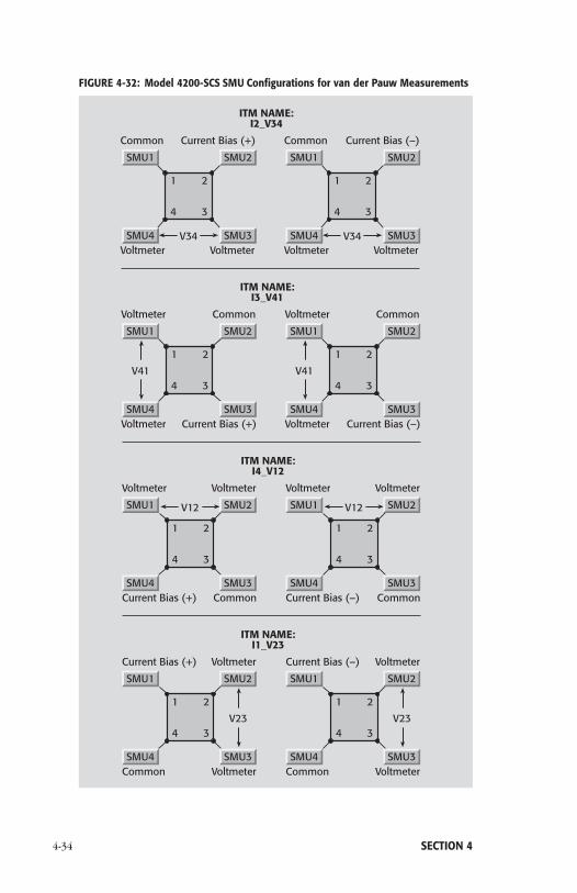
4-34 SECTION 4
4 3
1 2
Current Bias (+) Voltmeter
Common Voltmeter
4 3
1 2
Current Bias (–) Voltmeter
Common Voltmeter
ITM NAME:I1_V23
4 3
1 2
Voltmeter Voltmeter
Current Bias (+) Common
V12
4 3
1 2
Voltmeter Voltmeter
Current Bias (–) Common
V12
ITM NAME:I4_V12
4 3
1 2
Voltmeter Common
Voltmeter Current Bias (+)
V414 3
1 2
Voltmeter Common
Voltmeter Current Bias (–)
ITM NAME:I3_V41
4 3
1 2
Common Current Bias (+)
Voltmeter VoltmeterV34
4 3
1 2
Common Current Bias (–)
Voltmeter VoltmeterV34
ITM NAME:I2_V34
V41
V23 V23
SMU3
SMU2
SMU4
SMU1
SMU3
SMU2
SMU4
SMU1
SMU3
SMU2
SMU4
SMU1
SMU3
SMU2
SMU4
SMU1
SMU3
SMU2
SMU4
SMU1
SMU3
SMU2
SMU4
SMU1
SMU3
SMU2
SMU4
SMU1
SMU3
SMU2
SMU4
SMU1
FIGURE 4-32: Model 4200-SCS SMU Configurations for van der Pauw Measurements
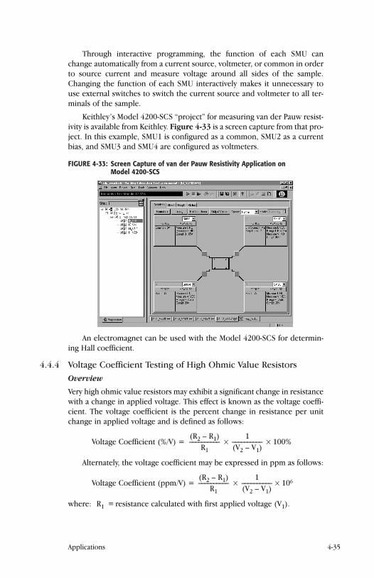
Through interactive programming, the function of each SMU canchange automatically from a current source, voltmeter, or common in orderto source current and measure voltage around all sides of the sample.Changing the function of each SMU interactively makes it unnecessary touse external switches to switch the current source and voltmeter to all ter-minals of the sample.
Keithley’s Model 4200-SCS “project” for measuring van der Pauw resist-ivity is available from Keithley. Figure 4-33 is a screen capture from that pro-ject. In this example, SMU1 is configured as a common, SMU2 as a currentbias, and SMU3 and SMU4 are configured as voltmeters.
FIGURE 4-33: Screen Capture of van der Pauw Resistivity Application on Model 4200-SCS
An electromagnet can be used with the Model 4200-SCS for determin-ing Hall coefficient.
4.4.4 Voltage Coefficient Testing of High Ohmic Value Resistors Overview
Very high ohmic value resistors may exhibit a significant change in resistancewith a change in applied voltage. This effect is known as the voltage coeffi-cient. The voltage coefficient is the percent change in resistance per unitchange in applied voltage and is defined as follows:
(R2 – R1) 1Voltage Coefficient (%/V) = __________ × __________ × 100%
R1 (V2 – V1)
Alternately, the voltage coefficient may be expressed in ppm as follows:
(R2 – R1) 1Voltage Coefficient (ppm/V) = __________ × __________ × 106
R1 (V2 – V1)
where: R1 = resistance calculated with first applied voltage (V1).
Applications 4-35
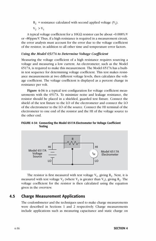
R2 = resistance calculated with second applied voltage (V2).
V2 > V1
A typical voltage coefficient for a 10GΩ resistor can be about –0.008%/Vor –80ppm/V. Thus, if a high resistance is required in a measurement circuit,the error analysis must account for the error due to the voltage coefficientof the resistor, in addition to all other time and temperature error factors.
Using the Model 6517A to Determine Voltage Coefficient
Measuring the voltage coefficient of a high resistance requires sourcing avoltage and measuring a low current. An electrometer, such as the Model6517A, is required to make this measurement. The Model 6517A has a built-in test sequence for determining voltage coefficient. This test makes resist-ance measurements at two different voltage levels, then calculates the volt-age coefficient. The voltage coefficient is displayed as a percent change inresistance per volt.
Figure 4-34 is a typical test configuration for voltage coefficient meas-urements with the 6517A. To minimize noise and leakage resistance, theresistor should be placed in a shielded, guarded test fixture. Connect theshield of the test fixture to the LO of the electrometer and connect the LOof the electrometer to the LO of the source. Connect the HI terminal of theelectrometer to one end of the resistor and the HI of the voltage source tothe other end.
FIGURE 4-34: Connecting the Model 6517A Electrometer for Voltage CoefficientTesting
The resistor is first measured with test voltage V1, giving R1. Next, it ismeasured with test voltage V2 (where V2 is greater than V1), giving R2. Thevoltage coefficient for the resistor is then calculated using the equationgiven in the overview.
4.5 Charge Measurement Applications The coulombmeter and the techniques used to make charge measurementswere described in Sections 1 and 2 respectively. Charge measurementsinclude applications such as measuring capacitance and static charge on
R
HI
LO
HI
LO
IMModel 6517A
VoltageSource
Model 6517AElectrometer
4-36 SECTION 4
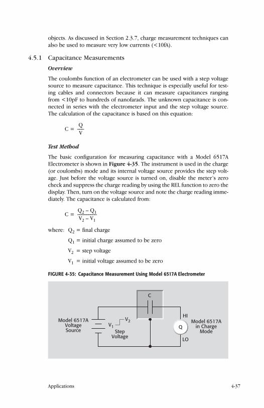
objects. As discussed in Section 2.3.7, charge measurement techniques canalso be used to measure very low currents (<10fA).
4.5.1 Capacitance Measurements
Overview
The coulombs function of an electrometer can be used with a step voltagesource to measure capacitance. This technique is especially useful for test-ing cables and connectors because it can measure capacitances rangingfrom <10pF to hundreds of nanofarads. The unknown capacitance is con-nected in series with the electrometer input and the step voltage source.The calculation of the capacitance is based on this equation:
QC = ___
V
Test Method
The basic configuration for measuring capacitance with a Model 6517AElectrometer is shown in Figure 4-35. The instrument is used in the charge(or coulombs) mode and its internal voltage source provides the step volt-age. Just before the voltage source is turned on, disable the meter’s zerocheck and suppress the charge reading by using the REL function to zero thedisplay. Then, turn on the voltage source and note the charge reading imme-diately. The capacitance is calculated from:
Q2 – Q1C = _________V2 – V1
where: Q2 = final charge
Q1 = initial charge assumed to be zero
V2 = step voltage
V1 = initial voltage assumed to be zero
FIGURE 4-35: Capacitance Measurement Using Model 6517A Electrometer
V2Model 6517AVoltageSource
QModel 6517A
in ChargeMode
HI
LO
C
V1Step
Voltage
Applications 4-37

After the reading has been recorded, reset the voltage source to 0V todissipate the charge from the device. Before handling the device, verify thecapacitance has been discharged to a safe level.
The unknown capacitance should be in a shielded test fixture. Theshield is connected to the LO input terminal of the electrometer. The HIinput terminal should be connected to the highest impedance terminal ofthe unknown capacitance. For example, when measuring the capacitance ofa length of coaxial cable, connect the HI terminal of the electrometer to thecenter conductor of the cable, allowing the cable shield to minimize elec-trostatic interference to the measurement.
If the rate of charge is too great, the resulting measurement will be inerror because the input stage becomes temporarily saturated. To limit therate of charge transfer at the input of the electrometer, add a resistor inseries between the voltage source and the capacitance. This is especiallytrue for capacitance values >1nF. A typical series resistor would be 10kΩ to1MΩ.
4.5.2 Using a Faraday Cup to Measure Static Charge on Objects
Overview
Insulators permit only a slight motion of electrons; therefore, electrostaticcharges can build up on a material and create hazards. The problem gener-ally is not the static charge itself on the object, but rather the spark gener-ated when the object discharges. Therefore, in order to understand andcontrol these problems, it’s necessary to measure the static electricity on anobject. This can be done by placing the object in a Faraday cup and meas-uring the charge with an electrometer. The Faraday cup method can be usedto measure the charge on a wide range of substances and objects, such asplastics, films, liquids, gases, and electronic components.
A Faraday cup (sometimes called a Faraday cage or icepail) is an enclo-sure made of sheet metal or conductive mesh. The electric field within aclosed, empty conductor is zero, so the cup shields the object placed insideit from any atmospheric or stray electric fields. This allows measuring thecharge on the object accurately.
Description of a Faraday Cup
Figure 4-36 illustrates a Faraday cup. It consists of two electrodes, oneinside the other, separated by an insulator. The inside electrode is connect-ed to the electrometer HI and the outside electrode is connected to theelectrometer LO. When a charged object is placed within the inside elec-trode, an induced charge will flow into the electrometer.
A Faraday cup can have virtually any dimensions, depending on the sizeand shape of the object to be tested. Cylindrical and spherical shapes aretypically the most convenient choices—simple containers like coffee orpaint cans are often used. The electrodes can be made of any conductive
4-38 SECTION 4
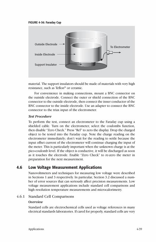
material. The support insulators should be made of materials with very highresistance, such as Teflon® or ceramic.
For convenience in making connections, mount a BNC connector onthe outside electrode. Connect the outer or shield connection of the BNCconnector to the outside electrode, then connect the inner conductor of theBNC connector to the inside electrode. Use an adapter to connect the BNCconnector to the triax input of the electrometer.
Test Procedure
To perform the test, connect an electrometer to the Faraday cup using ashielded cable. Turn on the electrometer, select the coulombs function,then disable “Zero Check.” Press “Rel” to zero the display. Drop the chargedobject to be tested into the Faraday cup. Note the charge reading on theelectrometer immediately; don’t wait for the reading to settle because theinput offset current of the electrometer will continue charging the input ofthe meter. This is particularly important when the unknown charge is at thepico-coulomb level. If the object is conductive, it will be discharged as soonas it touches the electrode. Enable “Zero Check” to re-zero the meter inpreparation for the next measurement.
4.6 Low Voltage Measurement Applications Nanovoltmeters and techniques for measuring low voltage were describedin Sections 1 and 3 respectively. In particular, Section 3.2 discussed a num-ber of error sources that can seriously affect precision measurements. Lowvoltage measurement applications include standard cell comparisons andhigh resolution temperature measurements and microcalorimetry.
4.6.1 Standard Cell Comparisons Overview
Standard cells are electrochemical cells used as voltage references in manyelectrical standards laboratories. If cared for properly, standard cells are very
Applications 4-39
To ElectrometerOutside Electrode
Inside Electrode
Support Insulator
FIGURE 4-36: Faraday Cup
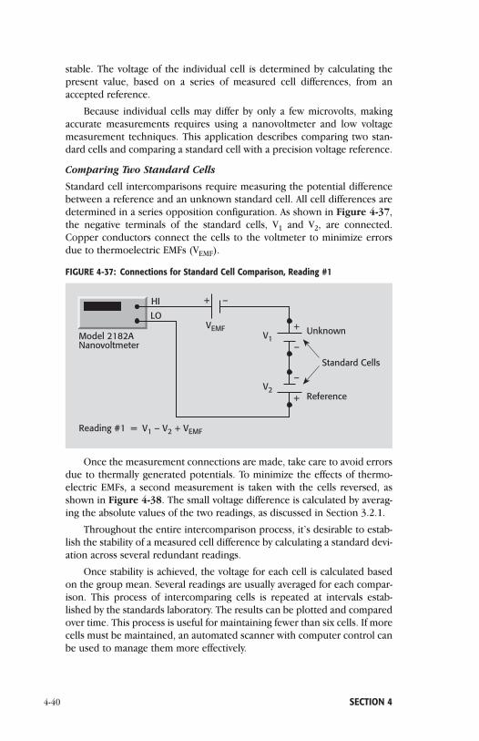
stable. The voltage of the individual cell is determined by calculating thepresent value, based on a series of measured cell differences, from anaccepted reference.
Because individual cells may differ by only a few microvolts, makingaccurate measurements requires using a nanovoltmeter and low voltagemeasurement techniques. This application describes comparing two stan-dard cells and comparing a standard cell with a precision voltage reference.
Comparing Two Standard Cells
Standard cell intercomparisons require measuring the potential differencebetween a reference and an unknown standard cell. All cell differences aredetermined in a series opposition configuration. As shown in Figure 4-37,the negative terminals of the standard cells, V1 and V2, are connected.Copper conductors connect the cells to the voltmeter to minimize errorsdue to thermoelectric EMFs (VEMF).
FIGURE 4-37: Connections for Standard Cell Comparison, Reading #1
Once the measurement connections are made, take care to avoid errorsdue to thermally generated potentials. To minimize the effects of thermo-electric EMFs, a second measurement is taken with the cells reversed, asshown in Figure 4-38. The small voltage difference is calculated by averag-ing the absolute values of the two readings, as discussed in Section 3.2.1.
Throughout the entire intercomparison process, it’s desirable to estab-lish the stability of a measured cell difference by calculating a standard devi-ation across several redundant readings.
Once stability is achieved, the voltage for each cell is calculated basedon the group mean. Several readings are usually averaged for each compar-ison. This process of intercomparing cells is repeated at intervals estab-lished by the standards laboratory. The results can be plotted and comparedover time. This process is useful for maintaining fewer than six cells. If morecells must be maintained, an automated scanner with computer control canbe used to manage them more effectively.
+Model 2182ANanovoltmeter
VEMF
HI
LO
V1
V2
–
–
+
Standard Cells
+ –
Reading #1 = V1 – V2 + VEMF
Unknown
Reference
4-40 SECTION 4
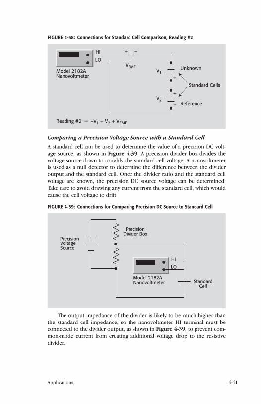
Comparing a Precision Voltage Source with a Standard Cell
A standard cell can be used to determine the value of a precision DC volt-age source, as shown in Figure 4-39. A precision divider box divides thevoltage source down to roughly the standard cell voltage. A nanovoltmeteris used as a null detector to determine the difference between the divideroutput and the standard cell. Once the divider ratio and the standard cellvoltage are known, the precision DC source voltage can be determined.Take care to avoid drawing any current from the standard cell, which wouldcause the cell voltage to drift.
FIGURE 4-39: Connections for Comparing Precision DC Source to Standard Cell
The output impedance of the divider is likely to be much higher thanthe standard cell impedance, so the nanovoltmeter HI terminal must beconnected to the divider output, as shown in Figure 4-39, to prevent com-mon-mode current from creating additional voltage drop to the resistivedivider.
Model 2182ANanovoltmeter
HI
LO
StandardCell
PrecisionVoltageSource
PrecisionDivider Box
Applications 4-41
–Model 2182ANanovoltmeter
VEMF
HI
LO
V1
V2
+
+
–
Standard Cells
+ –
Reading #2 = –V1 + V2 + VEMF
Unknown
Reference
FIGURE 4-38: Connections for Standard Cell Comparison, Reading #2
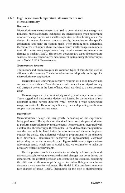
4.6.2 High Resolution Temperature Measurements andMicrocalorimetry Overview
Microcalorimetry measurements are used to determine various energy rela-tionships. Microcalorimetry techniques are often required when performingcalorimetric experiments with small sample sizes or slow heating rates. Thedesign of a microcalorimeter can vary greatly, depending on the specificapplication, and many are custom made. When running tests, differentialthermometry techniques allow users to measure small changes in tempera-ture. Microcalorimetry experiments may require measuring temperaturechanges as small as 100µ°C. This section describes two types of temperaturesensors and a microcalorimetry measurement system using thermocouplesand a Model 2182A Nanovoltmeter.
Temperature Sensors
Thermistors and thermocouples are common types of transducers used indifferential thermometry. The choice of transducer depends on the specificmicrocalorimetry application.
Thermistors are temperature-sensitive resistors with good linearity andaccuracy characteristics. These devices require an excitation signal, so theywill dissipate power in the form of heat, which may lead to a measurementerror.
Thermocouples are the most widely used type of temperature sensor.These rugged and inexpensive devices are formed by the junction of twodissimilar metals. Several different types, covering a wide temperaturerange, are available. Thermocouple linearity varies, depending on thermo-couple type and temperature range.
Description
Microcalorimeter design can vary greatly, depending on the experimentbeing performed. The application described here uses a simple calorimeterto perform microcalorimetry measurements. Temperature is measured witha differential thermocouple thermometer. In the differential configuration,one thermocouple is placed inside the calorimeter and the other is placedoutside the device. The difference voltage is proportional to the tempera-ture differential. Measurement sensitivity is approximately 25m°C/µV(depending on the thermocouple type). Figure 4-40 shows a typical micro-calorimeter setup, which uses a Model 2182A Nanovoltmeter to make thenecessary voltage measurements.
The temperature inside the calorimeter need only be known with mod-erate accuracy; however, to measure the small changes that occur during theexperiment, the greatest precision and resolution are essential. Measuringthe differential thermocouple’s signal to sub-millidegree resolutiondemands a very sensitive voltmeter. The Model 2182A can detect tempera-ture changes of about 100µ°C, depending on the type of thermocouple
4-42 SECTION 4
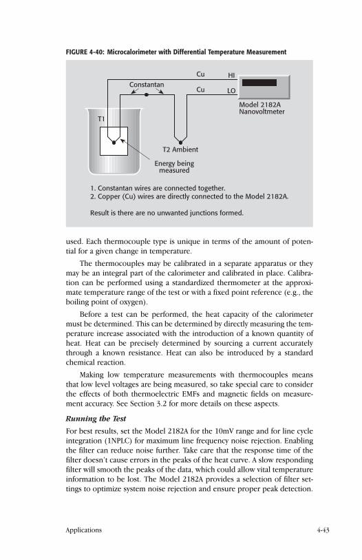
used. Each thermocouple type is unique in terms of the amount of poten-tial for a given change in temperature.
The thermocouples may be calibrated in a separate apparatus or theymay be an integral part of the calorimeter and calibrated in place. Calibra-tion can be performed using a standardized thermometer at the approxi-mate temperature range of the test or with a fixed point reference (e.g., theboiling point of oxygen).
Before a test can be performed, the heat capacity of the calorimetermust be determined. This can be determined by directly measuring the tem-perature increase associated with the introduction of a known quantity ofheat. Heat can be precisely determined by sourcing a current accuratelythrough a known resistance. Heat can also be introduced by a standardchemical reaction.
Making low temperature measurements with thermocouples meansthat low level voltages are being measured, so take special care to considerthe effects of both thermoelectric EMFs and magnetic fields on measure-ment accuracy. See Section 3.2 for more details on these aspects.
Running the Test
For best results, set the Model 2182A for the 10mV range and for line cycleintegration (1NPLC) for maximum line frequency noise rejection. Enablingthe filter can reduce noise further. Take care that the response time of thefilter doesn’t cause errors in the peaks of the heat curve. A slow respondingfilter will smooth the peaks of the data, which could allow vital temperatureinformation to be lost. The Model 2182A provides a selection of filter set-tings to optimize system noise rejection and ensure proper peak detection.
Applications 4-43
Model 2182ANanovoltmeter
Energy beingmeasured
T2 Ambient
T1
Cu HI
LO
1. Constantan wires are connected together.2. Copper (Cu) wires are directly connected to the Model 2182A.
Result is there are no unwanted junctions formed.
CuConstantan
FIGURE 4-40: Microcalorimeter with Differential Temperature Measurement
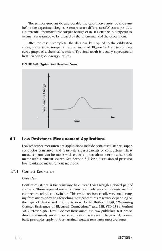
The temperature inside and outside the calorimeter must be the samebefore the experiment begins. A temperature difference of 0° corresponds toa differential thermocouple output voltage of 0V. If a change in temperatureoccurs, it’s assumed to be caused by the phenomena of the experiment.
After the test is complete, the data can be applied to the calibrationcurve, converted to temperature, and analyzed. Figure 4-41 is a typical heatcurve graph of a chemical reaction. The final result is usually expressed asheat (calories) or energy (joules).
FIGURE 4-41: Typical Heat Reaction Curve
4.7 Low Resistance Measurement Applications
Low resistance measurement applications include contact resistance, super-conductor resistance, and resistivity measurements of conductors. Thesemeasurements can be made with either a micro-ohmmeter or a nanovolt-meter with a current source. See Section 3.3 for a discussion of precisionlow resistance measurement methods.
4.7.1 Contact Resistance
Overview
Contact resistance is the resistance to current flow through a closed pair ofcontacts. These types of measurements are made on components such asconnectors, relays, and switches. This resistance is normally very small, rang-ing from micro-ohms to a few ohms. Test procedures may vary, depending onthe type of device and the application. ASTM Method B539, “MeasuringContact Resistance of Electrical Connections” and MIL-STD-1344 Method3002, “Low-Signal Level Contact Resistance” are two published test proce-dures commonly used to measure contact resistance. In general, certainbasic principles apply to four-terminal contact resistance measurements.
Time
Tem
pera
ture
Cha
nge
4-44 SECTION 4
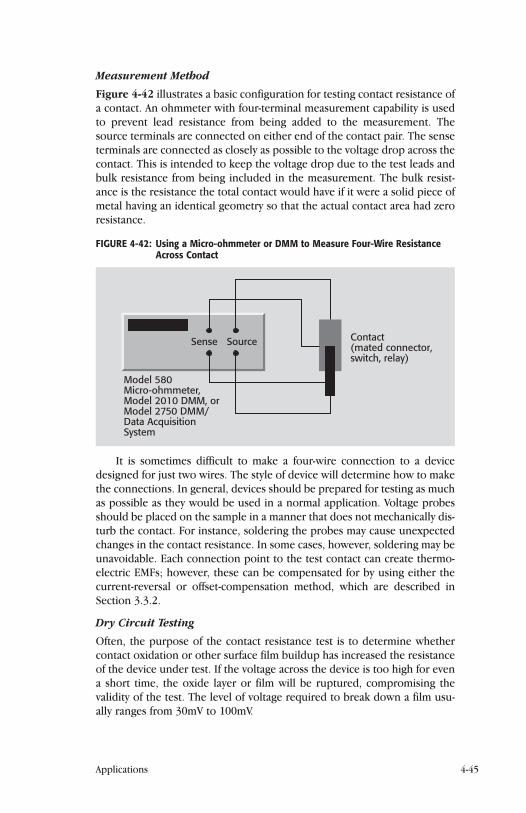
Measurement Method
Figure 4-42 illustrates a basic configuration for testing contact resistance ofa contact. An ohmmeter with four-terminal measurement capability is usedto prevent lead resistance from being added to the measurement. Thesource terminals are connected on either end of the contact pair. The senseterminals are connected as closely as possible to the voltage drop across thecontact. This is intended to keep the voltage drop due to the test leads andbulk resistance from being included in the measurement. The bulk resist-ance is the resistance the total contact would have if it were a solid piece ofmetal having an identical geometry so that the actual contact area had zeroresistance.
FIGURE 4-42: Using a Micro-ohmmeter or DMM to Measure Four-Wire Resistance Across Contact
It is sometimes difficult to make a four-wire connection to a devicedesigned for just two wires. The style of device will determine how to makethe connections. In general, devices should be prepared for testing as muchas possible as they would be used in a normal application. Voltage probesshould be placed on the sample in a manner that does not mechanically dis-turb the contact. For instance, soldering the probes may cause unexpectedchanges in the contact resistance. In some cases, however, soldering may beunavoidable. Each connection point to the test contact can create thermo-electric EMFs; however, these can be compensated for by using either thecurrent-reversal or offset-compensation method, which are described inSection 3.3.2.
Dry Circuit Testing
Often, the purpose of the contact resistance test is to determine whethercontact oxidation or other surface film buildup has increased the resistanceof the device under test. If the voltage across the device is too high for evena short time, the oxide layer or film will be ruptured, compromising thevalidity of the test. The level of voltage required to break down a film usu-ally ranges from 30mV to 100mV.
Sense
Model 580Micro-ohmmeter,Model 2010 DMM, orModel 2750 DMM/Data AcquisitionSystem
Source Contact(mated connector,switch, relay)
Applications 4-45
Excessive current through the contacts during testing can cause a physi-cal change in the contact area on a microscopic level. Current can cause heat-ing, which can soften or melt the contact points and the surrounding area.As a result, the contact area enlarges, resulting in a reduction in resistance.
To avoid these problems, the dry circuit method is usually employed forcontact resistance tests. A dry circuit is one in which the voltage and currentare limited to levels that can’t cause changes in the physical and electricalcondition of the contact junction. In general, that means the open circuitvoltage is 20mV or less and the short circuit current is 100mA or less.
Because of the low test current level used, a very sensitive voltmeter isrequired to measure the voltage drop, which is usually in the microvoltrange. Because of the potential for physical or electrical changes to the con-tact that other test methods pose, dry circuit measurements should be doneon the device before any other electrical tests are made.
Refer to Section 3.3.5 for further information on dry circuit testing.
Using a Micro-Ohmmeter or DMM
Figure 4-42 shows a basic configuration for making four-wire contact resist-ance measurements with a Model 580 Micro-ohmmeter, Model 2010 DMM,or Model 2750 DMM/Data Acquisition System. These instruments can auto-matically compensate for thermoelectric offsets in the sense circuit by usingthe Offset Compensation mode. They also have built-in dry circuit meas-urement capability. For most applications, the micro-ohmmeter or DMM issufficient for contact resistance measurements. If the short circuit current ormeasured resistance values are much smaller than the micro-ohmmeter’s orDMM’s specifications, a nanovoltmeter and a current source must be used.
Using a Nanovoltmeter and Current Source
Figure 4-43 illustrates a test configuration that employs a Model 2182ANanovoltmeter and a Series 2400 SourceMeter instrument for contact resist-ance measurements. The Series 2400 instrument forces a current throughthe contact and the nanovoltmeter measures the voltage drop developedacross the contact. For dry circuit testing, the open circuit voltage isclamped to 20mV by setting the SourceMeter compliance to 20mV. Toensure the compliance voltage is measured only across the contact and notacross the test leads, the SourceMeter is configured for the four-wire mode.This is especially important when higher currents are used because the volt-age drop across the test leads may be large compared to the voltage dropacross the contact. To prevent transients, always turn the source off whileswitching contacts in and out of the test fixture. A resistor, such as 100Ω,can be placed directly across the current source output terminals to reducetransients still further.
The current-reversal method can be used to minimize thermoelectricvoltage offsets. The Model 2182A’s Delta Mode feature and the SourceMeterinstrument make it possible to implement this technique automatically. In
4-46 SECTION 4
this mode, the Model 2182A automatically triggers the current source toalternate the polarity, then triggers a reading at each polarity. Then, theModel 2182A displays the “compensated” voltage value:
V1 – V2Delta V = ________2
The contact resistance may be calculated by:
Delta VRcontact = ________
I
where I = absolute value of test current.
4.7.2 Superconductor Resistance Measurements Overview
At extremely low temperatures, some metals and alloys lose their resistanceto electrical current and become superconductive. A superconductor’s tran-sition temperature and critical current density are two commonly measuredparameters. The superconducting transition temperature is the point atwhich a material’s resistance changes from a finite value to zero. The criti-cal current density is the maximum current density a material can carryunder specific temperature and magnetic field conditions before it becomesresistive. The higher these two parameters are, the better the superconduc-tor is. Determining these two parameters requires measuring very smallresistances, so a nanovoltmeter and a programmable current source areessential for precision measurements.
Test Description
Figure 4-44 shows a basic superconductor resistance measurement test sys-tem using the combination of a Model 2182A Nanovoltmeter and a Model6220 Current Source for measuring the resistance. The voltage leads shouldbe made of a material with a low Seebeck coefficient with respect to the
Applications 4-47
SenseSeries 2400SourceMeterInstrument
Output Rcontact Model 2182ANanovoltmeter
InputHI
LO
FIGURE 4-43: Using a Nanovoltmeter and Current Source to Measure Contact Resistance
sample. The sensitivity of the Model 2182A Nanovoltmeter is crucial toobtaining precision measurements because the application demands theability to measure extremely low voltages. If the application requires pico-volt resolution, the Model 1801 Nanovolt Preamplifier with the Model 2001or 2002 DMM can be used for even greater sensitivity.
For transition temperature measurements, the current source must bekept below the critical current of the sample. If the current becomes toohigh, the power dissipated may damage the sample and the cryostat. Forcritical current measurements, however, the current source must be able to
4-48 SECTION 4
Model 2182ANanovoltmeter
TemperatureController
Low Thermal Connector
Solid Copper Twisted Pair
HI LO
Tube (part ofsample holder)
Electrically isolatedfrom holder
SuperconductorSample
Sample Probe
Cryostat
HI LO
Model 6220Current Source
FIGURE 4-44: Superconductor Resistance Test System
exceed the critical current of the sample. If that means that more than100mA is needed (the current the Model 6220 Current Source can provide),a Model 2440 5A Current Source may be an appropriate solution. The cur-rent source should have programmable polarity, so the test can be per-formed using the current-reversal method.
The resistance is measured using the techniques described in Sections3.2 and 3.3 for low voltage and low resistance measurements. It is essentialthat a four-wire measurement be made. This technique eliminates leadresistance by forcing a current through the sample with one pair of leadswhile measuring the voltage drop with a second pair of leads. In addition,the Delta method is essential to eliminate the effects of changing thermo-electric EMFs, which may interfere with measurement accuracy.
The Delta method consists of measuring the voltage drop across thematerial with the current in one direction, then reversing the polarity of thecurrent source and taking a second voltage measurement. Three voltagemeasurements are used to calculate each resistance value. The Deltamethod is discussed in greater detail in Section 3.3.2. In cases where hys-teresis, non-linearity, or asymmetry is apparent, the current can be variedfrom one value to another of the same polarity. This will provide the aver-age resistance between these two currents.
The Model 2182A Nanovoltmeter and Model 6220 Current Source worktogether to implement the Delta method automatically. In this mode, theModel 6220 automatically alternates the polarity, then triggers the nano-voltmeter to take a reading at each polarity. Then, the Model 6220 displaysthe “compensated” resistance value.
As shown in Figure 4-45, the resistance can be plotted vs. temperatureas the sample temperature is changing.
Applications 4-49
FIGURE 4-45: Resistance vs. Temperature of Superconductor
Temperature(10K per division)
80 90 100
0
0.006
Resistance(0.0005Ω
per division)
77
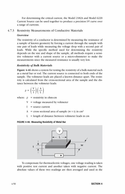
For determining the critical current, the Model 2182A and Model 6220Current Source can be used together to produce a precision I-V curve overa range of currents.
4.7.3 Resistivity Measurements of Conductive Materials
Overview
The resistivity of a conductor is determined by measuring the resistance ofa sample of known geometry by forcing a current through the sample withone pair of leads while measuring the voltage drop with a second pair ofleads. While the specific method used for determining the resistivitydepends on the size and shape of the sample, all methods require a sensi-tive voltmeter with a current source or a micro-ohmmeter to make themeasurements since the measured resistance is usually very low.
Resistivity of Bulk Materials
Figure 4-46 shows a system for testing the resistivity of a bulk material suchas a metal bar or rod. The current source is connected to both ends of thesample. The voltmeter leads are placed a known distance apart. The resist-ivity is calculated from the cross-sectional area of the sample and the dis-tance between the voltmeter leads:
V Aρ = ___ ___( I ) ( L )
where: ρ = resistivity in ohm-cm
V = voltage measured by voltmeter
I = source current
A = cross sectional area of sample (w × t) in cm2
L = length of distance between voltmeter leads in cm
FIGURE 4-46: Measuring Resistivity of Metal Bar
To compensate for thermoelectric voltages, one voltage reading is takenwith positive test current and another taken with negative current. Theabsolute values of these two readings are then averaged and used in the
V
L
t w
4-50 SECTION 4

equation for V/I. Most materials have a significant temperature coefficient,so be certain to maintain the sample at a known temperature.
Using a Four-Point Probe
The four-point probe method is used on very thin samples such as epitaxi-al wafers and conductive coatings. Figure 4-47 is a diagram of four-pointcollinear probe setup for resistivity measurements. The current is sourcedthrough the two outer probes and the voltage drop is measured betweenthe two inner probes. The surface or sheet resistivity is calculated by:
π Vσ = ____ ___( ln2 ) ( I )
where: σ = sheet resistivity in ohms/square
V = voltage measured by voltmeter
I = source current
FIGURE 4-47: Using a Four-Point Collinear Probe on Wafer
Note that the units for sheet resistivity are expressed as ohms persquare in order to distinguish this number from the measured resistance(V/I). Correction factors to the resistivity calculation may be required forextremely thin or thick samples.
If the thickness of the sample is known, the bulk or volume resistivitycan be calculated from
π Vρ = ____ ___ t( ln2 ) ( I )
where: ρ = volume resistivity in ohm-cm
t = thickness in centimeters
Further information on four-point probe measurements can be foundin the ASTM standard F84.
van der Pauw Method
Although van der Pauw resistivity measurements are used primarily in thesemiconductor industry, they have other applications, such as determiningthe resistivity of superconductors or foil. The van der Pauw method is used
V
Applications 4-51
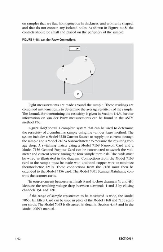
on samples that are flat, homogeneous in thickness, and arbitrarily shaped,and that do not contain any isolated holes. As shown in Figure 4-48, thecontacts should be small and placed on the periphery of the sample.
FIGURE 4-48: van der Pauw Connections
Eight measurements are made around the sample. These readings arecombined mathematically to determine the average resistivity of the sample.The formula for determining the resistivity is given in Section 4.4.3. Furtherinformation on van der Pauw measurements can be found in the ASTMmethod F76.
Figure 4-49 shows a complete system that can be used to determinethe resistivity of a conductive sample using the van der Pauw method. Thesystem includes a Model 6220 Current Source to supply the current throughthe sample and a Model 2182A Nanovoltmeter to measure the resulting volt-age drop. A switching matrix using a Model 7168 Nanovolt Card and aModel 7156 General Purpose Card can be constructed to switch the volt-meter and current source among the four sample terminals. The cards mustbe wired as illustrated in the diagram. Connections from the Model 7168card to the sample must be made with untinned copper wire to minimizethermoelectric EMFs. These connections from the 7168 must then beextended to the Model 7156 card. The Model 7001 Scanner Mainframe con-trols the scanner cards.
To source current between terminals 3 and 4, close channels 7L and 4H.Measure the resulting voltage drop between terminals 1 and 2 by closingchannels 15L and 12H.
If the range of sample resistivities to be measured is wide, the Model7065 Hall Effect Card can be used in place of the Model 7168 and 7156 scan-ner cards. The Model 7065 is discussed in detail in Section 4.4.3 and in theModel 7065’s manual.
V
4
3
2
1
4-52 SECTION 4
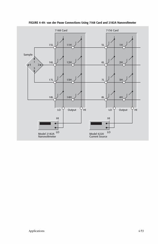
Applications 4-53
1
34 2
Model 2182ANanovoltmeter
HI
LOModel 6220Current Source
HI
LO
15L 11H
16L 12H
17L 13H
18L 14H
LO HIOutput
5L 1H
6L 2H
7L 3H
8L 4H
LO HIOutput
7168 Card 7156 Card
Sample
FIGURE 4-49: van der Pauw Connections Using 7168 Card and 2182A Nanovoltmeter
S E C T I O N 5
Low LevelInstrument
Selection Guide
5.1 IntroductionChoosing a specific low level instrument for a given application depends ona variety of factors, including:
• Functions (voltage, current, resistance, charge)
• Ranges and sensitivity
• Special features required (battery operation, floating operation, etc.)
• Convenience features (IEEE-488 interfaceability, auto-ranging, datastorage, etc.)
• Price
• Compatibility with other equipment in the test setup (analog output,overload protection, external triggers, etc.)
This section provides an overview of low level instruments availablefrom Keithley. Consult Keithley’s Test and Measurement Products Catalogfor further details on any of the products covered in this book (and manyother products not listed).
5.2 Instrument and Accessory Selector GuidesFigure 5-1 is a function/range comparison chart for Keithley’s low levelinstrumentation. Tables 5-1 through 5-9 summarize the capabilities ofthese instruments and the various accessories designed for use with them.
5-2 SECTION 5

LOW LEVEL INSTRUMENT SELECTION GUIDE 5-3
FIG
URE
5-1:
Low
Leve
lIns
trum
entF
unct
ion/
Rang
eSe
lect
ion
Char
t
Sens
itiv
eVo
ltm
eter
s
Sour
ce/M
easu
reU
nits
(SM
U)
Sour
ceM
eter
Inst
rum
ents
Pico
amm
eter
s
Elec
trom
eter
s
Low
Res
ista
nce
Met
ers
1801
/200
121
82A
236
237
238
4200
-SM
U42
10-S
MU
4200
-SM
Uw
/420
0-PA
4210
-SM
Uw
/420
0-PA
2400
2410
2420
2425
2430
2440
6430 428
6485
6487
DC
Volts
DC
Amps
Ohm
sC
oulo
mbs
E–15
E–12
E–9
E–6
E–3
E0E3
E6E9
E15
E12
E18
1f1p
1n1µ
1m1
1k1M
1G1P
1T1E
580
1801
/200
120
1027
50
6514
6517
A
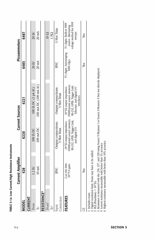
Curr
entA
mpl
ifier
Curr
entS
ourc
esPi
coam
met
ers
MO
DEL
428
6220
6221
6485
6487
CURR
ENT
From
1.2
fA1
100
fAD
C10
0fA
DC
(1pA
AC)
20fA
120
fA1
To10
mA
100
mA
DC
100
mA
DC
(100
mA
AC)
20m
A20
mA
RESI
STAN
CE4
From
510
ΩTo
61
PΩIn
put
Conn
ectio
nBN
CO
utpu
tcon
nect
ions
:3
Slot
Tria
x.O
utpu
tcon
nect
ions
:3
Slot
Tria
xBN
C3
Slot
Tria
x
FEAT
URE
S2
µsris
etim
e.10
11V/
Aga
in.
1014
Ωou
tput
impe
danc
e.65
000-
poin
tsou
rce
mem
ory.
RS-2
32,G
PIB,
Trig
gerL
ink,
and
digi
talI
/O.
1014
Ωou
tput
impe
danc
e.65
000-
poin
tsou
rce
mem
ory.
RS-2
32,G
PIB,
Trig
gerL
ink,
Ethe
rnet
,and
digi
talI
/Oin
terfa
ces.
51 ⁄2di
gits
.Aut
oran
ging
.10
00rd
g/s.
51 ⁄2di
gits
.Bui
lt-in
500V
sour
ce.A
ltern
atin
gvo
ltage
met
hod
forH
I-Rsw
eeps
.
CEYe
sYe
sYe
s1.
Incl
udes
noise
.2.
Dig
italr
esol
utio
nlim
it.N
oise
may
have
tobe
adde
d.3.
PΩ(P
etao
hms)
=10
15Ω
.4.
Resis
tanc
eis
mea
sure
dw
ithth
e23
6,23
7,an
d23
8us
ing
Sour
ceV/
Mea
sure
IorS
ourc
eI/M
easu
reV,
butn
otdi
rect
lydi
spla
yed.
5.Lo
wes
tres
istan
cem
easu
rabl
ew
ithbe
ttert
han
1%ac
cura
cy.
6.H
ighe
stre
sista
nce
mea
sura
ble
with
bette
rtha
n10
%ac
cura
cy.
5-4 SECTION 5
TABL
E5-
1a:L
owCu
rren
t/H
igh
Resi
stan
ceIn
stru
men
ts
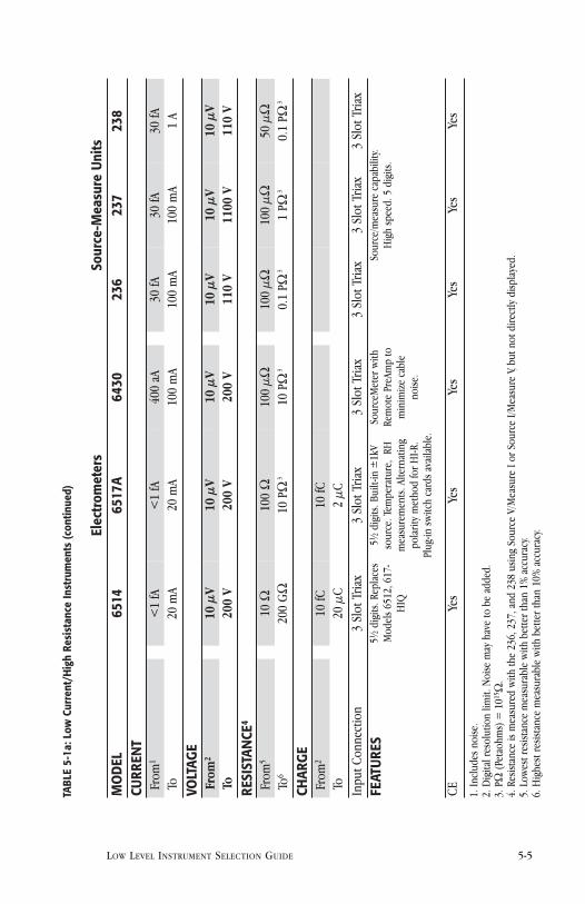
Elec
trom
eter
sSo
urce
-Mea
sure
Uni
tsM
OD
EL65
1465
17A
6430
236
237
238
CURR
ENT
From
1<
1fA
<1
fA40
0aA
30fA
30fA
30fA
To20
mA
20m
A10
0m
A10
0m
A10
0m
A1
A
VOLT
AGE
From
210
µV
10µ
V10
µV
10µ
V10
µV
10µ
VTo
200
V20
0V
200
V11
0V
1100
V11
0V
RESI
STAN
CE4
From
510
Ω10
0Ω
100
µΩ10
0µΩ
100
µΩ50
µΩTo
620
0G
Ω10
PΩ3
10PΩ
30.
1PΩ
31
PΩ3
0.1
PΩ3
CHAR
GE
From
210
fC10
fCTo
20µC
2µC
Inpu
tCon
nect
ion
3Sl
otTr
iax
3Sl
otTr
iax
3Sl
otTr
iax
3Sl
otTr
iax
3Sl
otTr
iax
3Sl
otTr
iax
FEAT
URE
S51 ⁄2
digi
ts.R
epla
ces
Mod
els
6512
,617
-H
IQ
51 ⁄2di
gits
.Bui
lt-in
±1k
Vso
urce
.Tem
pera
ture
,RH
mea
sure
men
ts.A
ltern
atin
gpo
larit
ym
etho
dfo
rHI-R
.Pl
ug-in
switc
hca
rds
avai
labl
e.
Sour
ceM
eter
with
Rem
ote
PreA
mp
tom
inim
ize
cabl
eno
ise.
Sour
ce/m
easu
reca
pabi
lity.
Hig
hsp
eed.
5di
gits
.
CEYe
sYe
sYe
sYe
sYe
sYe
s
1.In
clud
esno
ise.
2.D
igita
lres
olut
ion
limit.
Noi
sem
ayha
veto
bead
ded.
3.PΩ
(Pet
aohm
s)=
1015
Ω.
4.Re
sista
nce
ism
easu
red
with
the
236,
237,
and
238
usin
gSo
urce
V/M
easu
reIo
rSou
rce
I/Mea
sure
V,bu
tnot
dire
ctly
disp
laye
d.5.
Low
estr
esist
ance
mea
sura
ble
with
bette
rtha
n1%
accu
racy
.6.
Hig
hest
resis
tanc
em
easu
rabl
ew
ithbe
ttert
han
10%
accu
racy
.
LOW LEVEL INSTRUMENT SELECTION GUIDE 5-5
TABL
E5-
1a:L
owCu
rren
t/H
igh
Resi
stan
ceIn
stru
men
ts(c
ontin
ued)
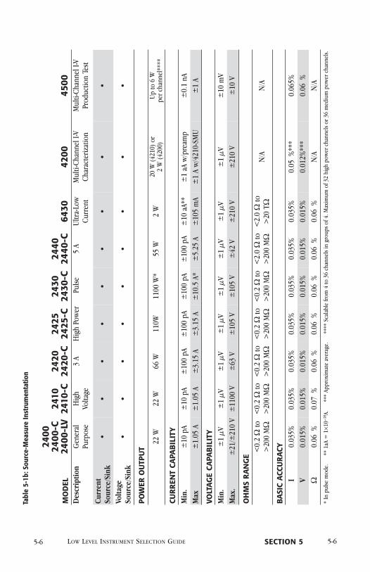
5-6 SECTION 5LOW LEVEL INSTRUMENT SELECTION GUIDE 5-6
Tabl
e5-
1b:S
ourc
e-M
easu
reIn
stru
men
tatio
n
MO
DEL
2400
2400
-C24
00-L
V24
1024
10-C
2420
2420
-C24
2524
25-C
2430
2430
-C24
4024
40-C
6430
4200
4500
Des
crip
tion
Gen
eral
Purp
ose
Hig
hVo
ltage
3A
Hig
hPo
wer
Pulse
5A
Ultr
a-Lo
wCu
rren
tM
ulti-
Chan
nelI
-VCh
arac
teriz
atio
nM
ulti-
Chan
nelI
-VPr
oduc
tion
Test
Curr
ent
Sour
ce/S
ink
••
••
••
••
•
Volta
geSo
urce
/Sin
k•
••
••
••
••
POW
ERO
UTP
UT
22W
22W
66W
110W
1100
W*
55W
2W
20W
(421
0)or
2W
(420
0)Up
to6
Wpe
rcha
nnel
****
CUR
REN
TCA
PAB
ILIT
Y
Min
.±
10pA
±10
pA±
100
pA±
100
pA±
100
pA±
100
pA±
10aA
**±
1aA
w/p
ream
p±
0.1
nAM
ax±
1.05
A±
1.05
A±
3.15
A±
3.15
A±
10.5
A*±
5.25
A±
105
mA
±1
Aw
/421
0-SM
U±
1A
VOLT
AG
ECA
PAB
ILIT
Y
Min
.±
1µV
±1
µV±
1µV
±1
µV±
1µV
±1
µV±
1µV
±1
µV±
10m
VM
ax.
±21
/±21
0V
±11
00V
±63
V±
105
V±
105
V±
42V
±21
0V
±21
0V
±10
V
OH
MS
RA
NG
E<
0.2
Ωto
>20
0M
Ω<
0.2
Ωto
>20
0M
Ω<
0.2
Ωto
>20
0M
Ω<
0.2
Ωto
>20
0M
Ω<
0.2
Ωto
>20
0M
Ω<
2.0
Ωto
>20
0M
Ω<
2.0
Ωto
>20
TΩN
/AN
/A
BA
SIC
ACC
UR
ACY
I0.
035%
0.03
5%0.
035%
0.03
5%0.
035%
0.03
5%0.
035%
0.05
%**
*0.
065%
V0.
015%
0.01
5%0.
015%
0.01
5%0.
015%
0.01
5%0.
015%
0.01
2%**
*0.
06%
Ω0.
06%
0.07
%0.
06%
0.06
%0.
06%
0.06
%0.
06%
N/A
N/A
*In
pulse
mod
e.**
1aA
=1×
10–1
8 A.
***
Appr
oxim
ate
aver
age.
****
Scal
able
from
4to
36ch
anne
lsin
grou
psof
4.M
axim
umof
32hi
ghpo
wer
chan
nels
or36
med
ium
pow
erch
anne
ls.

LOW LEVEL INSTRUMENT SELECTION GUIDE 5-75-7 SECTION 5
Tabl
e5-
1c:L
owVo
ltage
and
Low
Resi
stan
ceM
easu
rem
entI
nstr
umen
ts
1801
wit
hM
OD
EL58
020
01or
2002
2182
A20
0220
1027
50Vo
ltage
From
—1
pV1
nV1
nV10
nV10
0nV
To2
mV
100
V10
00V
1000
V10
00V
Inpu
tVol
tage
Nois
e—
0.12
nVrm
s1.
2nV
rms
150
nVrm
s10
0nV
rms
<1.
5µV
rms
Resi
stan
ceFr
om1
200
µΩ20
µΩ10
nΩ3
1.2
mΩ
0.9
mΩ
0.4
mΩ
To2
200
kΩ20
0Ω
(1G
Ω)5
100
MΩ
31
GΩ
100
MΩ
100
MΩ
Ther
moc
oupl
eTe
mpe
ratu
reFr
om—
–200
°C–2
00°C
–200
°C–2
00°C
–200
°CTo
1820
°C18
20°C
1820
°C13
72°C
1820
°C
Inpu
tCon
nect
ion
Bana
naja
cks
(4)
Copp
ernu
tsSp
ecia
llow
Bana
naja
cks
(4)
Bana
naja
cks
(4)
Bana
naja
cks
(4)
Fron
tinp
uts
only
ther
moe
lect
ricw
/cop
perp
ins
Spec
ialF
eatu
res
Dry
circu
it.M
ulti-
func
tion.
DEL
TAm
ode.
81 ⁄2di
gits.
Dry
circu
it.D
rycir
cuit.
Offs
etco
mpe
nsat
ion.
Tem
pera
ture
.An
alog
outp
ut.
DM
M.
Offs
etco
mpe
nsat
ion.
Offs
etco
mpe
nsat
ion.
Batte
ry(o
pt.)
IEEE
-488
.IE
EE-4
88.
IEEE
-488
.D
MM
.D
MM
.D
MM
.RS
-232
.Pl
ug-in
scan
ner
IEEE
-488
.RS-
232.
IEEE
-488
.RS-
232.
card
s.Pl
ug-in
scan
ner
Dig
italI
/O.
card
s.Pl
ug-in
mod
ules
.
CEYe
s4—
Yes
Yes
Yes
Yes
1.Lo
wes
tres
istan
cem
easu
rabl
ew
ithbe
ttert
han
10%
accu
racy
.2.
Hig
hest
resis
tanc
em
easu
rabl
ew
ithbe
ttert
han
1%ac
cura
cy.
3.D
elta
mod
e,of
fset
volta
geco
mpe
nsat
ion
with
exte
rnal
curr
ents
ourc
e.10
nΩif
used
with
5Ate
stcu
rren
twith
Mod
el24
40.
4.Ex
clud
esIE
EE-4
88op
tion.
5.1G
Ωif
Mod
el18
01is
bypa
ssed
usin
gM
odel
2002
,100
MΩ
ifby
pass
edan
dus
ing
Mod
el20
01.
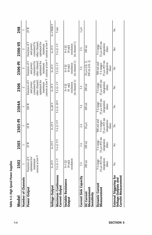
5-8 SECTION 5
Tabl
e5-
2:H
igh
Spee
dPo
wer
Supp
lies
Mod
el23
0223
0323
03-P
J23
04A
2306
2306
-PJ
2306
-VS
248
Num
ber
ofCh
anne
ls1
11
12
22
1
Pow
erO
utpu
tFu
nctio
nof
V;op
timiz
edfo
rm
axim
umcu
rren
tatl
owV
45W
45W
100
WFu
nctio
nof
Van
dpo
wer
cons
umed
byot
herc
hann
el;
optim
ized
for
max
imum
curr
enta
tlow
V
Func
tion
ofV
and
pow
erco
nsum
edby
othe
rcha
nnel
;op
timiz
edfo
rm
axim
umcu
rren
tatl
owV
Func
tion
ofV
and
pow
erco
nsum
edby
othe
rcha
nnel
;op
timiz
edfo
rm
axim
umcu
rren
tatl
owV
25W
Volt
age
Out
put
0–15
V0–
15V
0–15
V0–
20V
0–15
V0–
15V
0–15
V0–
±50
00V
Max
imum
Cont
inuo
usCu
rren
tO
utpu
t5
A@
4V
5A
@9
V5
A@
9V
5A
@20
V5
A@
4V
5A
@4
V5
A@
4V
5m
A
Vari
able
Res
ista
nce
Out
put
0–1
Ω10
mΩ
reso
lutio
n
0–1
Ω10
mΩ
reso
lutio
n(in
chan
nel1
)
0–1
Ω10
mΩ
reso
lutio
n(in
chan
nel1
)
0–1
Ω10
mΩ
reso
lutio
n(in
chan
nel1
)
Curr
ent
Sink
Capa
city
3A
2A
2A
3A
3A
3A
3A
1µ
A
DC
Curr
ent
Mea
sure
men
tSe
nsit
ivit
y
100
nA10
0nA
10µ
A10
0nA
100
nA10
µA
(Ch.
1)10
0nA
(Ch.
2)10
0nA
Dyn
amic
Curr
ent
Mea
sure
men
t5
Ara
nge:
33µs
–833
ms
inte
grat
ion
times
5A
rang
e:33
µs–8
33m
sin
tegr
atio
ntim
es
500
mA
and
5A
rang
es:
33µs
–833
ms
inte
grat
ion
times
5A
rang
e:33
µs–8
33m
sin
tegr
atio
ntim
es
5A
rang
e:33
µs–8
33m
sin
tegr
atio
ntim
es
500
mA
and
5A
rang
es:
33µs
–833
ms
inte
grat
ion
times
5A
rang
e:33
µs–8
33m
sin
tegr
atio
ntim
es
Exte
rnal
Trig
geri
ngfo
rVo
ltag
eO
utpu
tsan
dCu
rren
tM
easu
rem
ent
No
No
No
No
No
No
Yes
No
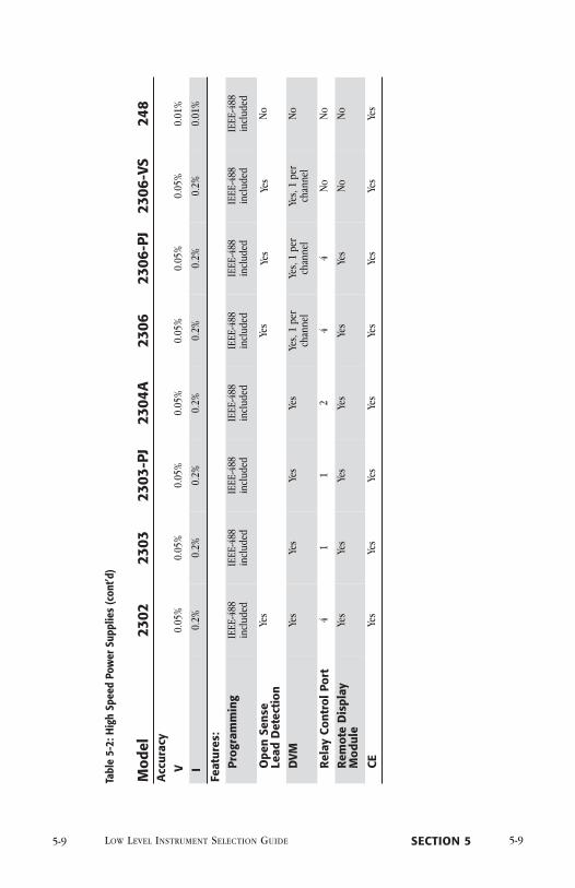
LOW LEVEL INSTRUMENT SELECTION GUIDE 5-95-9 SECTION 5
Tabl
e5-
2:H
igh
Spee
dPo
wer
Supp
lies
(con
t’d)
Mod
el23
0223
0323
03-P
J23
04A
2306
2306
-PJ
2306
-VS
248
Acc
urac
yV
0.05
%0.
05%
0.05
%0.
05%
0.05
%0.
05%
0.05
%0.
01%
I0.
2%0.
2%0.
2%0.
2%0.
2%0.
2%0.
2%0.
01%
Feat
ures
:Pr
ogra
mm
ing
IEEE
-488
incl
uded
IEEE
-488
incl
uded
IEEE
-488
incl
uded
IEEE
-488
incl
uded
IEEE
-488
incl
uded
IEEE
-488
incl
uded
IEEE
-488
incl
uded
IEEE
-488
incl
uded
Ope
nSe
nse
Lead
Det
ecti
onYe
sYe
sYe
sYe
sN
o
DVM
Yes
Yes
Yes
Yes
Yes,
1pe
rch
anne
lYe
s,1
per
chan
nel
Yes,
1pe
rch
anne
lN
o
Rel
ayCo
ntro
lPo
rt4
11
24
4N
oN
o
Rem
ote
Dis
play
Mod
ule
Yes
Yes
Yes
Yes
Yes
Yes
No
No
CEYe
sYe
sYe
sYe
sYe
sYe
sYe
sYe
s
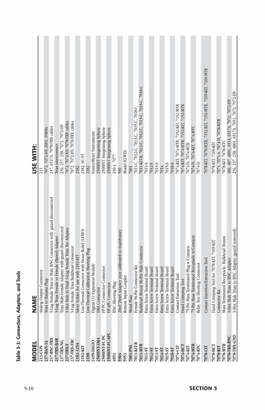
5-10 SECTION 5
Tabl
e5-
3:Co
nnec
tors
,Ada
pter
s,an
dTo
ols
MO
DEL
NA
ME
USE
WIT
H:
213-
CON
Anal
ogO
utpu
tCon
nect
or21
323
7-BA
N-3
ATr
iax
toBa
nana
Plug
7072
,707
2-H
V,20
01,D
MM
s23
7-BN
C-T
RX3-
Lug
Fem
ale
Tria
xto
Mal
eBN
CCo
nnec
torw
ithgu
ard
disc
onne
cted
237,
6517
A,70
78-T
RXca
bles
237-
TRX-
BAR
3-Lu
gTr
iax
Fem
ale
toFe
mal
e(B
arre
l)Ad
apte
rTr
iax
inte
rcon
nect
237-
TRX-
NG
Tria
xM
ale-
Fem
ale
Adap
terw
ithgu
ard
disc
onne
cted
236,
237,
238,
7072
,707
2-H
V23
7-TR
X-T
3-Sl
otM
ale
toD
ual3
-Lug
Fem
ale
Tria
xTe
eAd
apte
r70
72,7
072-
HV,
7078
-TRX
cabl
es23
7-TR
X-TB
C3-
Lug
Fem
ale
Tria
xBu
lkhe
adCo
nnec
tor
7072
,707
2-H
V,70
78-T
RXca
bles
2182
-325
ASi
lver
Sold
erfo
ruse
with
2182
-KIT
2182
2182
-KIT
Low
-The
rmal
Conn
ecto
rwith
Stra
inRe
lief(
LEM
O)
2182
,SC-
9321
88Lo
w-T
herm
alCa
libra
tion
Shor
ting
Plug
2182
2499
-DIG
IOD
igita
lI/O
Expa
nsio
nM
odul
eSo
urce
Met
erIn
stru
men
ts25
00IN
T-SM
ASM
ACo
nnec
tor
2500
INT
Inte
grat
ing
Sphe
re25
00IN
T-FC
/PC
FP/P
CCo
nnec
torC
onne
ctor
2500
INT
Inte
grat
ing
Sphe
re25
00IN
T-FC
/APC
FP/A
PCCo
nnec
tor
2500
INT
Inte
grat
ing
Sphe
re48
51BN
CSh
ortin
gPl
ug23
0-1,
7077
5904
20nF
/20m
SAd
apte
r(no
tcal
ibra
ted
tom
ainf
ram
e)59
059
51Re
mot
eIn
putC
oupl
erM
odel
82-W
IN70
01-P
NL
Met
alPl
ate
7001
7011
-KIT
-RFe
mal
e96
-Pin
Conn
ecto
rKit
7011
-C,7
012-
C,70
13-C
,701
5-C,
7018
-C70
11-M
TRBu
lkhe
adM
ount
96-P
inM
ale
Conn
ecto
r70
11-K
IT-R
,701
1-C,
7012
-C,7
013-
C,70
15-C
,701
8-C
7011
-ST
Extr
aSc
rew
Term
inal
Boar
d70
11-S
7012
-ST
Extr
aSc
rew
Term
inal
Boar
d70
12-S
7013
-ST
Extr
aSc
rew
Term
inal
Boar
d70
13-S
7014
-ST
Extr
aSc
rew
Term
inal
Boar
d70
1470
15-S
TEx
tra
Scre
wTe
rmin
alBo
ard
7015
-S70
18-S
TEx
tra
Scre
wTe
rmin
alBo
ard
7018
-S70
74-C
ITCo
ntac
tExt
ract
ion
Tool
7074
-KIT
,707
4-M
TR,7
152-
KIT,
7152
-MTR
7074
-HCT
Han
dCr
impi
ngTo
ol70
74-K
IT,7
074-
MTR
,715
2-KI
T,71
52-M
TR70
74-K
IT75
-Pin
Mas
sTe
rmin
ated
Plug
w/C
onta
cts
7074
-D,7
074-
MTR
7074
-MTR
75-P
inM
ass
Term
inat
edRe
cept
acle
w/C
onta
cts
7074
-D,7
074-
KIT,
7074
-MTC
7074
-RTC
Rela
yTe
stSh
ortin
gCo
nnec
tor
7074
-D
7078
-CIT
Cont
actI
nser
tion/
Extr
actio
nTo
ol70
78-K
IT,7
078-
MTR
,715
2-KI
T,71
52-M
TR,7
169-
KIT,
7169
-MTR
7078
-HCT
Han
dCr
impi
ngTo
olfo
r707
8-KI
T,71
69-K
IT70
78-K
IT,7
169-
KIT
7078
-KIT
Conn
ecto
rKit
7071
,707
1-4,
7074
-D,7
078-
MTR
7078
-MTR
Mas
sTe
rmin
ated
Rece
ptac
le,B
ulkh
ead
Mou
nt70
78-K
IT,7
078-
MTC
7078
-TRX
-BN
C3-
Slot
Mal
eTr
iax
toBN
CAd
apte
r48
6,48
7,48
01,6
514,
6517
A,70
72,7
072-
HV
7078
-TRX
-GN
D3-
Slot
Mal
eTr
iax
toBN
CAd
apte
r(gu
ard
rem
oved
)23
6,23
7,23
8,48
01,6
517A
,705
1,70
72,7
072-
HV
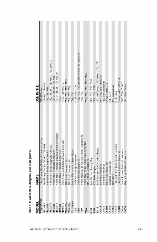
LOW LEVEL INSTRUMENT SELECTION GUIDE 5-11
Tabl
e5-
3:Co
nnec
tors
,Ada
pter
s,an
dTo
ols
(con
t’d)
MO
DEL
NA
ME
USE
WIT
H:
7078
-TRX
-TBC
3-Lu
gFe
mal
eTr
iax
Bulk
head
Conn
ecto
rw/C
ap70
78-T
RXca
bles
7152
-HCT
Han
dCr
imp
Tool
for7
152-
KIT,
7152
-MTR
7152
-KIT
,715
2-M
TR71
52-K
IT6-
Posit
ion
M-S
erie
sPl
ugw
/Con
tact
s71
52,7
152-
MTR
7152
-MTR
6-Po
sitio
nM
-Ser
ies
Rece
ptac
lew
/Soc
kets
7152
,715
2-KI
T,71
52-M
TC-2
,715
2-M
TC-1
071
64-K
IT50
-Pin
Mas
sTe
rmin
ated
Conn
ecto
r71
64-D
,716
4-M
,716
4-M
TR71
64-M
TR50
-Pin
Mas
sTe
rmin
ated
Bulk
head
Mou
ntRe
cept
acle
7164
-D,7
164-
M,7
164-
MTC
-10
7169
-KIT
20-P
inM
ass
Term
inat
edCo
nnec
tor
7169
A71
69-M
TRM
ass
Term
inat
edBu
lkhe
adM
ount
Rece
ptac
le71
69A,
7169
-MTC
-377
03-3
06A
DB5
0M
ale
Conn
ecto
rKit
7701
,770
3,77
05,7
709
7709
-308
AD
B25
Mal
eCo
nnec
torK
it77
01,7
707,
7709
7712
-SM
A-N
Fem
ale
SMA
toM
ale
N-Ty
peAd
apte
r77
11,7
712
7755
50Ω
Feed
-Thr
ough
Term
inat
orRG
58Ca
ble,
776
7788
50-P
inD
Subc
onne
ctor
Kit
7703
,770
5,77
XX,m
odul
esw
ithD
sub
conn
ecto
rs77
8950
-Pin
Mal
ean
d25
-Pin
Mal
eD
-She
llCo
nnec
torK
it77
01,7
709
7790
50-P
inM
ale,
50-P
inFe
mal
e,an
d25
-Pin
Mal
eID
CD
-She
llCo
nnec
torK
it77
01,7
703,
7705
,770
7,77
09
8610
Low
Ther
mal
Shor
ting
Plug
2000
,200
1,20
02,2
010
8680
RTD
Prob
eAd
apte
r20
01,2
002,
2010
BG-1
8D
ualB
anan
ato
BNC
Coax
ialA
dapt
er23
0,20
XXSe
ries,
24XX
Serie
s,27
00,2
750
CAP-
18Pr
otec
tive
Shie
ld/C
apBN
C,2-
lug
tria
xco
nnec
tors
CAP-
31Pr
otec
tive
Shie
ld/C
ap3-
lug
tria
xco
nnec
tors
CS-4
00D
B25
Mal
eSo
lder
Cup
CA-1
26-1
cabl
e,21
3CS
-458
Inte
rlock
Conn
ecto
rKit
6517
-ILC-
3CS
-565
BNC
Barr
elBN
Cin
terc
onne
ctCS
-631
3-Lu
gM
ale
Tria
xCa
ble
Mou
ntCo
nnec
tor
SC-2
2Ca
ble
CS-6
803-
Lug
Fem
ale
Bulk
head
Conn
ecto
rFi
xtur
es,6
487,
6517
A,et
c.CS
-846
Scre
wTe
rmin
alTe
stLe
adCo
nnec
tor
230X
,251
0,25
10-A
TCS
-970
Hig
hVo
ltage
Bulk
head
Conn
ecto
r24
8,24
8-SH
VCa
ble
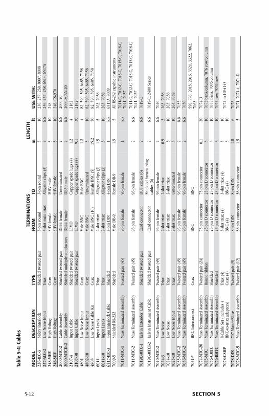
5-12 SECTION 5
Tabl
e5-
4:Ca
bles
MO
DEL
DES
CRIP
TIO
NTY
PE
TER
MIN
ATIO
NS
LEN
GTH
USE
WIT
H:
FRO
MTO
mft
236-
ILC
-3Sa
fety
Inte
rlock
Shie
lded
twist
edpa
ir3-
pin
roun
d3-
pin
roun
d3
1023
6,23
7,23
8,80
07,8
008
237-
ALG
-2Lo
wN
oise
Inpu
tTr
iax
3-slo
tmal
etr
iax
Allig
ator
clip
s(3
)2
6.6
236,
237,
238,
6514
,651
7A24
8-M
HV
Hig
hVo
ltage
Coax
SHV
fem
ale
MH
Vm
ale
310
248
248-
SHV
Hig
hVo
ltage
Coax
SHV
fem
ale
SHV
fem
ale
310
248,
CS-
970
2000
-MTC
-2Ca
ble
Asse
mbl
ySh
ield
edtw
isted
pair
DB4
4fe
mal
eUn
term
inat
ed2
6.6
2000
-20
2000
-MTC
D-2
Cabl
eAs
sem
bly
Shie
lded
mul
tiple
cond
ucto
rsD
B44
fem
ale
DB5
0m
ale
26.
620
00-S
CAN
-20
2107
-4In
putC
able
Shie
lded
twist
edpa
irLE
MO
Copp
ersp
ade
lugs
(4)
1.2
421
8221
07-3
0In
putC
able
Shie
lded
twist
edpa
irLE
MO
Copp
ersp
ade
lugs
(4)
9.1
3021
8248
01Lo
wN
oise
Inpu
tCo
axM
ale
BNC
Mal
eBN
C1.
24
82,5
90,5
95,6
485,
7158
4802
-10
Low
Noi
seIn
put
Coax
Mal
eBN
CUn
term
inat
ed3
1082
,590
,595
,648
5,71
5848
03Lo
wN
oise
Cabl
eKi
tCo
axM
ale
BNC
(10)
Fem
ale
BNC
(5)
15.2
5082
,590
,595
,648
5,71
5860
11In
putL
eads
Tria
x2-
slott
riax
Allig
ator
clip
s(3
)1.
55
263,
7058
6011
-10
Inpu
tLea
dsTr
iax
2-slo
ttria
xAl
ligat
orcl
ips
(3)
310
263,
7058
6517
-ILC
-34-
pin
Inte
rlock
Cabl
eSh
ield
ed4-
pin
DIN
4-pi
nD
IN1
3.3
6517
A,80
0970
09-5
Shie
lded
RS-2
32Sh
ield
edM
ale
DB-
9Fe
mal
eD
B-9
1.5
5Al
lRS-
232
capa
ble
inst
rum
ents
7011
-MTC
-1M
ass
Term
inat
edAs
sem
bly
Twist
edpa
ir(4
5)96
-pin
fem
ale
96-p
infe
mal
e1
3.3
7011
-C,7
012-
C,70
13-C
,701
5-C,
7018
-C,
7021
,703
7
7011
-MTC
-2M
ass
Term
inat
edAs
sem
bly
Twist
edpa
ir(4
5)96
-pin
fem
ale
96-p
infe
mal
e2
6.6
7011
-C,7
012-
C,70
13-C
,701
5-C,
7018
-C,
7021
,703
770
19C
-MTC
-1Ke
lvin
Exte
nder
Cabl
eSh
ield
edtw
isted
pair
Card
conn
ecto
rD
UTca
bles
(6)
26.
670
19-C
7019
C-M
TCI-2
Kelv
inIn
stru
men
tCab
leSh
ield
edtw
isted
pair
Card
conn
ecto
rSh
ield
edba
nana
plug
cabl
es(6
)2
6.6
7019
-C,2
400
Serie
s
7020
-MTC
-2M
ass
Term
inat
edAs
sem
bly
Twist
edpa
ir(4
5)96
-pin
fem
ale
96-p
infe
mal
e2
6.6
7020
7024
-3Lo
wN
oise
Tria
x2-
slott
riax
2-slo
ttria
x0.
93
263,
7058
7024
-10
Low
Noi
seTr
iax
2-slo
ttria
x2-
slott
riax
310
263,
7058
7025
-10
Low
Noi
seIn
put
Tria
x2-
slott
riax
Unte
rmin
ated
310
263,
7058
7035
-MTC
-2M
ass
Term
inat
edAs
sem
bly
Twist
edpa
ir(4
5)96
-pin
fem
ale
96-p
infe
mal
e2
6.6
7035
7036
-MTC
-2M
ass
Term
inat
edAs
sem
bly
Twist
edpa
ir(4
5)96
-pin
fem
ale
96-p
infe
mal
e2
6.6
7036
7051
-*BN
CIn
terc
onne
ctCo
axBN
CBN
C59
0,77
6,20
15,2
016,
3321
,332
2,70
62,
7063
7074
-MTC
-20
Mas
sTe
rmin
ated
Asse
mbl
yTw
isted
pair
(24)
75-p
inco
nnec
tor
75-p
inco
nnec
tor
6.1
2070
74-D
7075
-MTC
Mas
sTe
rmin
ated
Asse
mbl
yRo
und
ribbo
n25
-pin
Dco
nnec
tor
25-p
inD
conn
ecto
r3
1070
75ba
nk/c
olum
n,70
76ro
w/c
olum
n70
76-C
MTC
Mas
sTe
rmin
ated
Asse
mbl
ySh
ield
ed25
-pin
Dco
nnec
tor
25-p
inD
conn
ecto
r3
1070
75ba
nk,7
076
colu
mn
7076
-RM
TCM
ass
Term
inat
edAs
sem
bly
Shie
lded
25-p
inD
conn
ecto
r25
-pin
Dco
nnec
tor
310
7075
row,
7076
row
7078
-CSH
P8-
Cabl
eSe
t(in
clud
es4
BNC-
to-tr
iax
adap
ters
)Tr
iax
(4)
Coax
(4)
3-slo
ttria
x(4
)BN
C(4
)3-
slott
riax
(4)
BNC
(4)
3 310 10
7072
toH
P-41
45
7078
-DIN
707
Mas
ter/S
lave
Twist
edpa
ir(9
)8-
pin
DIN
8-pi
nD
IN1.
86
707A
7078
-MTC
-5M
ass
Term
inat
edAs
sem
bly
Twist
edpa
ir(1
2)38
-pin
conn
ecto
r38
-pin
conn
ecto
r1.
55
7071
,707
1-4,
7074
-D
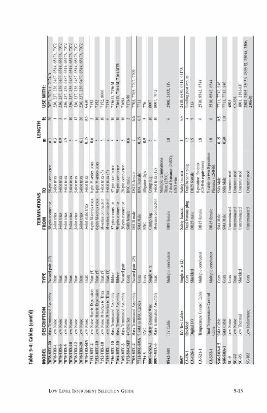
LOW LEVEL INSTRUMENT SELECTION GUIDE 5-13
Tabl
e5-
4:Ca
bles
(con
t’d)
MO
DEL
DES
CRIP
TIO
NTY
PE
TER
MIN
ATIO
NS
LEN
GTH
USE
WIT
H:
FRO
MTO
mft
7078
-MTC
-20
Mas
sTe
rmin
ated
Asse
mbl
yTw
isted
pair
(12)
38-p
inco
nnec
tor
38-p
inco
nnec
tor
6.1
2070
71,7
071-
4,70
74-D
7078
-TRX
-1Lo
wN
oise
Tria
x3-
slott
riax
3-slo
ttria
x0.
31
236,
237,
238,
6487
,651
4,65
17A,
7072
7078
-TRX
-3Lo
wN
oise
Tria
x3-
slott
riax
3-slo
ttria
x0.
93
236,
237,
238,
6487
,651
4,65
17A,
7072
7078
-TRX
-5Lo
wN
oise
Tria
x3-
slott
riax
3-slo
ttria
x1.
55
236,
237,
238,
6487
,651
4,65
17A,
7072
7078
-TRX
-10
Low
Noi
seTr
iax
3-slo
ttria
x3-
slott
riax
310
236,
237,
238,
6487
,651
4,65
17A,
7072
7078
-TRX
-12
Low
Noi
seTr
iax
3-slo
ttria
x3-
slott
riax
412
236,
237,
238,
6487
,651
4,65
17A,
7072
7078
-TRX
-20
Low
Noi
seTr
iax
3-slo
ttria
x3-
slott
riax
6.1
2023
6,23
7,23
8,64
87,6
514,
6517
A,70
7270
78-T
RX-6
INLo
wN
oise
Tria
x3-
slotm
ale
tria
x3-
slott
riax
0.15
0.5
6430
7152
-MTC
-2Lo
wN
oise
Mat
rixEx
pans
ion
Tria
x(5
)6-
pin
M-se
ries
coax
6-pi
nM
-serie
sco
ax0.
62
7152
7152
-MTC
-10
Low
Noi
seM
atrix
Expa
nsio
nTr
iax
(5)
6-pi
nM
-serie
sco
ax6-
pin
M-se
ries
coax
310
7152
7152
-TRX
-10
Low
Noi
seM
-Ser
ies
toTr
iax
Tria
x(5
)M
-serie
sco
nnec
tor
3-slo
ttria
x(5
)3
1071
52,8
006
7153
-TRX
Low
Noi
seM
-Ser
ies
toTr
iax
Tria
x(5
)M
-serie
sco
nnec
tor
3-slo
ttria
x(5
)2
671
5371
56-M
TC-1
0M
ass
Term
inat
edAs
sem
bly
Ribb
on37
-pin
conn
ecto
r37
-pin
conn
ecto
r3
1071
56-D
,715
6-M
7164
-MTC
-10
Mas
sTe
rmin
ated
Asse
mbl
yRi
bbon
50-p
inco
nnec
tor
50-p
inco
nnec
tor
310
7164
-D,7
164-
M,7
164-
MTR
7169
-MTC
-3M
ass
Term
inat
edAs
sem
bly
Twist
edpa
ir20
-pin
conn
ecto
r20
-pin
conn
ecto
r3
1071
69A
7173
-50-
CSEP
4-Ca
ble
Set
Coax
SMB
fem
ale
BNC
mal
e0.
62
7173
-50
7705
-MTC
-2M
ass
Term
inat
edAs
sem
bly
Twist
edpa
ir(2
5)D
SUB
mal
eD
SUB
fem
ale
26.
677
03,7
705,
7707
,770
977
11-B
NC
-SM
A5
SMA
toBN
CCa
bles
Coax
SMA
Mal
eBN
CFe
mal
e0.
150.
577
1177
54-3
BNC
Coax
BNC
Allig
ator
clip
s0.
93
776
8007
-GN
D-3
Safe
tyG
roun
dW
ireSi
ngle
wire
Crim
plu
gCr
imp
lug
310
8007
8007
-MTC
-3M
ass
Term
inat
edAs
sem
bly
Tria
xM
-serie
sco
nnec
tor
3-slo
ttria
x(1
2)3
1080
07,7
072
8542
-301
LIV
Cabl
eM
ultip
leco
nduc
tor
DB9
fem
ale
Mul
tiple
term
inat
ions
:Tr
iax
(250
0);
2du
alba
nana
s(2
4XX)
;G
ND
wire
1.8
625
00,2
4XX,
LIV
8607
1kV
Test
Cabl
esSi
ngle
wire
(2)
Safe
tyba
nana
Safe
tyba
nana
13.
324
10,6
430,
6514
,651
7ACA
-18-
1Sh
ield
edCo
axD
ualb
anan
apl
ugD
ualb
anan
apl
ug1.
24
Bind
ing
post
inpu
tsCA
-126
-1D
igita
lI/O
Shie
lded
DB2
5m
ale
DB2
5fe
mal
e1.
55
213
CA-3
21-1
Tem
pera
ture
Cont
rolC
able
Mul
tiple
cond
ucto
rD
B15
fem
ale
8-po
sitio
nPh
oeni
x(C
S-84
6eq
uiva
lent
)1.
86
2510
,854
2,85
44
CA-3
22-1
Dua
lTem
pera
ture
Cont
rol
Cabl
eM
ultip
leco
nduc
tor
DB1
5fe
mal
eY
cabl
eto
two
8-po
sitio
nPh
oeni
x(C
S-84
6)1.
86
2510
,854
2,85
44
S46-
SMA-
0.5
SMA
Cabl
eCo
axSM
AM
ale
SMA
Mal
e0.
150.
577
11,7
712,
S46
S46-
SMA-
1SM
ACa
ble
Coax
SMA
Mal
eSM
AM
ale
0.30
1.0
7711
,771
2,S4
6SC
-9Lo
wN
oise
Coax
Unte
rmin
ated
Unte
rmin
ated
4803
SC-2
2Lo
wN
oise
Tria
xUn
term
inat
edUn
term
inat
edC
S-63
1SC
-93
Low
Ther
mal
Shie
lded
Unte
rmin
ated
Unte
rmin
ated
1801
,218
2-KI
T
SC-1
82Lo
wIn
duct
ance
Coax
Unte
rmin
ated
Unte
rmin
ated
2302
,230
3,23
03B,
2303
-PJ,
2304
A,23
06,
2306
-PJ
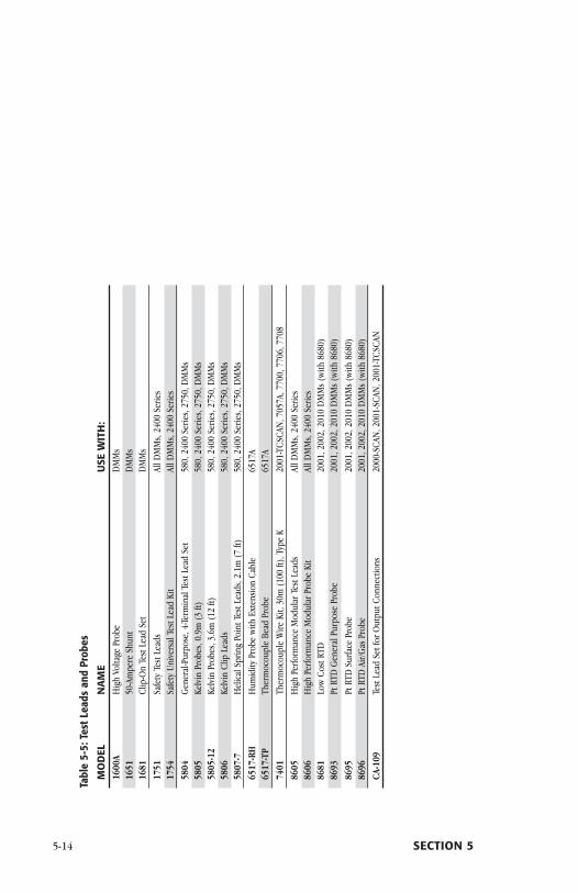
5-14 SECTION 5
Tabl
e5-
5:Te
stLe
ads
and
Prob
es
MO
DEL
NA
ME
USE
WIT
H:
1600
AH
igh
Volta
gePr
obe
DM
Ms
1651
50-A
mpe
reSh
unt
DM
Ms
1681
Clip
-On
Test
Lead
Set
DM
Ms
1751
Safe
tyTe
stLe
ads
AllD
MM
s,24
00Se
ries
1754
Safe
tyUn
iver
salT
estL
ead
Kit
AllD
MM
s,24
00Se
ries
5804
Gen
eral
-Pur
pose
,4-Te
rmin
alTe
stLe
adSe
t58
0,24
00Se
ries,
2750
,DM
Ms
5805
Kelv
inPr
obes
,0.9
m(3
ft)58
0,24
00Se
ries,
2750
,DM
Ms
5805
-12
Kelv
inPr
obes
,3.6
m(1
2ft)
580,
2400
Serie
s,27
50,D
MM
s58
06Ke
lvin
Clip
Lead
s58
0,24
00Se
ries,
2750
,DM
Ms
5807
-7H
elic
alSp
ring
Poin
tTes
tLea
ds,2
.1m
(7ft)
580,
2400
Serie
s,27
50,D
MM
s
6517
-RH
Hum
idity
Prob
ew
ithEx
tens
ion
Cabl
e65
17A
6517
-TP
Ther
moc
oupl
eBe
adPr
obe
6517
A
7401
Ther
moc
oupl
eW
ireKi
t,30
m(1
00ft)
,Typ
eK
2001
-TC
SCAN
,705
7A,7
700,
7706
,770
8
8605
Hig
hPe
rform
ance
Mod
ular
Test
Lead
sAl
lDM
Ms,
2400
Serie
s86
06H
igh
Perfo
rman
ceM
odul
arPr
obe
Kit
AllD
MM
s,24
00Se
ries
8681
Low
Cost
RTD
2001
,200
2,20
10D
MM
s(w
ith86
80)
8693
PtRT
DG
ener
alPu
rpos
ePr
obe
2001
,200
2,20
10D
MM
s(w
ith86
80)
8695
PtRT
DSu
rface
Prob
e20
01,2
002,
2010
DM
Ms
(with
8680
)86
96Pt
RTD
Air/G
asPr
obe
2001
,200
2,20
10D
MM
s(w
ith86
80)
CA-1
09Te
stLe
adSe
tfor
Out
putC
onne
ctio
ns20
00-S
CAN
,200
1-SC
AN,2
001-
TCSC
AN
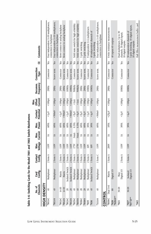
LOW LEVEL INSTRUMENT SELECTION GUIDE 5-15
Tabl
e5-
6:Sw
itchi
ngCa
rds
for
the
Mod
el70
01an
d70
02Sw
itch
Mai
nfra
mes
Max
.N
o.of
Card
Cont
act
Max
.M
ax.
Max
.Co
ntac
tO
ffse
tRe
com
m.
Conn
ectio
nCh
anne
lsCo
nfig.
Confi
g.Vo
ltage
Curr
ent
Pow
erPo
tent
ial
Curr
ent
Freq
uenc
yTy
peCE
Com
men
ts
HIG
HD
ENSI
TY70
11-C
40M
ultip
lexe
r2
form
A11
0V1A
60VA
<1µ
V<
100p
A2M
Hz
Conn
ecto
rYe
sFo
urin
depe
nden
t1×1
0m
ultip
lexe
rs,
conn
ectio
nto
back
plan
e70
11-S
40M
ultip
lexe
r2
form
A11
0V1A
60VA
<50
0nV
<10
0pA
2MH
zSc
rew
term
.Ye
sFo
urin
depe
nden
t1×1
0m
ultip
lexe
rs,
conn
ectio
nto
back
plan
e70
12-C
4×10
Mat
rix2
form
A11
0V1A
60VA
<1µ
V<
100p
A2M
Hz
Conn
ecto
rYe
sRo
ws
conn
ectt
oan
alog
back
plan
e70
12-S
4×10
Mat
rix2
form
A11
0V1A
60VA
<50
0nV
<10
0pA
2MH
zSc
rew
term
.Ye
sRo
ws
conn
ectt
oan
alog
back
plan
e70
13-C
20Is
olat
edSw
itch
2fo
rmA
110V
1A60
VA<
1µV
<10
0pA
10M
Hz
Conn
ecto
rYe
s70
13-S
20Is
olat
edSw
itch
2fo
rmA
110V
1A60
VA<
500n
V<
100p
A10
MH
zSc
rew
term
.Ye
s70
15-C
40M
ultip
lexe
r2
form
A17
5V34
mA
0.3V
A<
5µV
<1n
A50
0kH
zCo
nnec
tor
Yes
Solid
stat
esw
itch
forh
igh
relia
bilit
y70
15-S
40M
ultip
lexe
r2
form
A17
5V34
mA
0.3V
A<
5µV
<1n
A50
0kH
zSc
rew
term
.Ye
sSo
lidst
ate
switc
hfo
rhig
hre
liabi
lity
7018
-C28
Mul
tiple
xer
3fo
rmA
110V
1A60
VA<
5µV
<10
0pA
2MH
zCo
nnec
tor
Yes
3po
lesw
itchi
ng70
18-S
28M
ultip
lexe
r3
form
A11
0V1A
60VA
<5µ
V<
100p
A2M
Hz
Scre
wte
rm.
Yes
3po
lesw
itchi
ng70
3536
Mul
tiple
xer
2fo
rmA
60V
1A30
VA<
1µV
<10
0pA
10M
Hz
Conn
ecto
rYe
s9
inde
pend
ent1
×4m
ultip
lexe
rs70
3640
Isol
ated
Switc
h1
form
A60
V1A
30VA
<4µ
V<
100p
A10
MH
zCo
nnec
tor
Yes
40in
depe
nden
tcha
nnel
sof
1-po
lesw
itchi
ng71
11-S
40M
ultip
lexe
r1
form
C11
0V1A
60VA
<50
0nV
<10
0pA
2MH
zSc
rew
term
.Ye
sFo
urin
depe
nden
t1×1
0m
ultip
lexe
rs,
conn
ectio
nto
back
plan
e
CON
TRO
L70
19-C
Dua
l3×6
Mat
rix1
form
A20
0V1A
10VA
<25
µV<
100p
A2M
Hz
Conn
ecto
rYe
s6-
wire
resis
tanc
em
easu
rem
ents
7020
80D
igita
lI/O
Conn
ecto
rYe
s40
inpu
ts/4
0ou
tput
s70
20-D
**
7021
30/2
0M
ux/
Dua
lmul
tiple
xers
.Up
to30
Dig
italI
/O2
form
A11
0V1A
30VA
<3µ
V<
100p
A10
MH
zCo
nnec
tor
Yes
chan
nels,
10di
gita
linp
uts,
10di
gita
lout
puts
.
7037
30/2
0Is
olat
ed/
1fo
rmA
110V
1A30
VA<
4µV
<10
0pA
10M
Hz
Conn
ecto
rYe
s30
inde
pend
entc
hann
els
of70
37-D
**D
igita
lI/O
1-po
lesw
itchi
ng,1
0di
gita
linp
uts,
10di
gita
lout
puts
7065
Hal
lEffe
ctm
easu
rem
entb
uffe
rcar
d
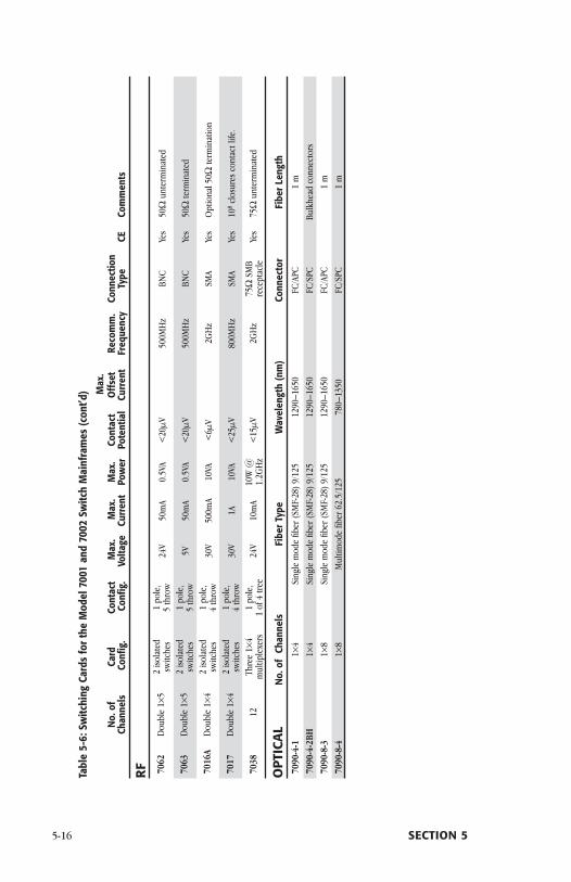
5-16 SECTION 5
Tabl
e5-
6:Sw
itchi
ngCa
rds
for
the
Mod
el70
01an
d70
02Sw
itch
Mai
nfra
mes
(con
t’d) M
ax.
No.
ofCa
rdCo
ntac
tM
ax.
Max
.M
ax.
Cont
act
Off
set
Reco
mm
.Co
nnec
tion
Chan
nels
Confi
g.Co
nfig.
Volta
geCu
rren
tPo
wer
Pote
ntia
lCu
rren
tFr
eque
ncy
Type
CECo
mm
ents
RF 70
62D
oubl
e1×
52
isola
ted
1po
le,
switc
hes
5th
row
24V
50m
A0.
5VA
<20
µV50
0MH
zBN
CYe
s50
Ωun
term
inat
ed
7063
Dou
ble
1×5
2iso
late
d1
pole
,sw
itche
s5
thro
w5V
50m
A0.
5VA
<20
µV50
0MH
zBN
CYe
s50
Ωte
rmin
ated
7016
AD
oubl
e1×
42
isola
ted
1po
le,
switc
hes
4th
row
30V
500m
A10
VA<
6µV
2GH
zSM
AYe
sO
ptio
nal5
0Ωte
rmin
atio
n
7017
Dou
ble
1×4
2iso
late
d1
pole
,sw
itche
s4
thro
w30
V1A
10VA
<25
µV80
0MH
zSM
AYe
s10
8cl
osur
esco
ntac
tlife
.
7038
12Th
ree
1×4
1po
le,
24V
10m
A10
W@
<15
µV2G
Hz
75Ω
SMB
Yes
75Ω
unte
rmin
ated
mul
tiple
xers
1of
4tr
ee1.
2GH
zre
cept
acle
OPT
ICA
LN
o.of
Chan
nels
Fibe
rTy
peW
avel
engt
h(n
m)
Conn
ecto
rFi
ber
Leng
th
7090
-4-1
1×4
Sing
lem
ode
fiber
(SM
F-28
)9/1
2512
90–1
650
FC/A
PC1
m
7090
-4-2
BH1×
4Si
ngle
mod
efib
er(S
MF-
28)9
/125
1290
–165
0FC
/SPC
Bulk
head
conn
ecto
rs
7090
-8-3
1×8
Sing
lem
ode
fiber
(SM
F-28
)9/1
2512
90–1
650
FC/A
PC1
m
7090
-8-4
1×8
Mul
timod
efib
er62
.5/1
2578
0–13
50FC
/SPC
1m
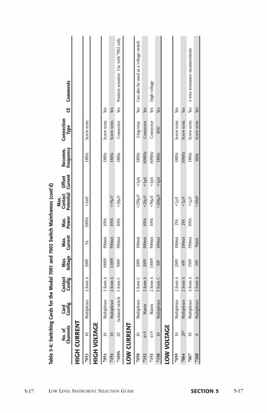
LOW LEVEL INSTRUMENT SELECTION GUIDE 5-175-17 SECTION 5
Tabl
e5-
6:Sw
itchi
ngCa
rds
for
the
Mod
el70
01an
d70
02Sw
itch
Mai
nfra
mes
(con
t’d)
Max
.N
o.of
Card
Cont
act
Max
.M
ax.
Max
.Co
ntac
tO
ffse
tRe
com
m.
Conn
ectio
nCh
anne
lsCo
nfig.
Confi
g.Vo
ltage
Curr
ent
Pow
erPo
tent
ial
Curr
ent
Freq
uenc
yTy
peCE
Com
men
ts
HIG
HCU
RR
ENT
7053
10M
ultip
lexe
r2
form
A30
0V5A
100V
A<
1mV
1MH
zSc
rew
term
.
HIG
HVO
LTA
GE
7054
10M
ultip
lexe
r1
form
A10
00V
500m
A10
VA1M
Hz
Scre
wte
rm.
Yes
7154
10M
ultip
lexe
r2
form
A11
00V
500m
A10
VA<
35µV
1MH
zSc
rew
term
.Ye
s
7169
A20
Isol
ated
switc
h1
form
C50
0V50
0mA
10VA
<30
µV2M
Hz
Conn
ecto
rYe
sPo
sitio
nse
nsiti
ve.U
sew
ith70
02on
ly.
LOW
CUR
REN
T70
5810
Mul
tiple
xer
1fo
rmC
200V
100m
A<
250µ
V<
1pA
3MH
z2-
lug
tria
xYe
sCa
nal
sobe
used
asa
volta
gesw
itch
7152
4×5
Mat
rix2
form
A20
0V50
0mA
10VA
<20
µV<
1pA
60M
Hz
Conn
ecto
rYe
s
7153
4×5
Mat
rix2
form
A13
00V
500m
A10
VA<
50µV
<1p
A60
MH
zCo
nnec
tor
Yes
Hig
hvo
ltage
7158
10M
ultip
lexe
r1
form
C30
V10
0mA
<20
0µV
<1p
A1M
Hz
BNC
Yes
LOW
VOLT
AG
E70
5910
Mul
tiple
xer
2fo
rmA
200V
100m
A2V
A<
1µV
3MH
zSc
rew
term
.Ye
s
7064
20*
Mul
tiple
xer
2fo
rmA
40V
100m
A2V
A<
1µV
10M
Hz
Scre
wte
rm.
Yes
7067
10M
ultip
lexe
r4
form
A15
0V35
0mA
10VA
<1µ
V1M
Hz
Scre
wte
rm.
Yes
4w
irere
sista
nce
mea
sure
men
ts
7168
8M
ultip
lexe
r2
form
A10
V50
mA
<30
nV1k
Hz
Scre
wte
rm.
Yes
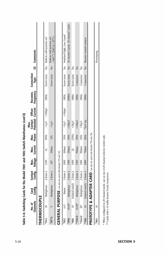
5-18 SECTION 5
Tabl
e5-
6:Sw
itchi
ngCa
rds
for
the
Mod
el70
01an
d70
02Sw
itch
Mai
nfra
mes
(con
t’d)
Max
.N
o.of
Card
Cont
act
Max
.M
ax.
Max
.Co
ntac
tO
ffse
tRe
com
m.
Conn
ectio
nCh
anne
lsCo
nfig.
Confi
g.Vo
ltage
Curr
ent
Pow
erPo
tent
ial
Curr
ent
Freq
uenc
yTy
peCE
Com
men
ts
THER
MO
COU
PLE
7014
39M
ultip
lexe
r2
form
A11
0V1A
60VA
<1µ
V<
100p
A2M
Hz
Scre
wte
rm.
Yes
Built
-inco
ldju
nctio
nre
f.
7057
A9
Mul
tiple
xer
2fo
rmA
42V
100m
A2V
A<
1µV
Scre
wte
rm.
Yes
Built
-inco
ldju
nctio
nre
f:–1
mV/
°C(0
mV
at+
30°C
)
GEN
ERA
LP
UR
POSE
Can
also
beus
edw
ithM
odel
s70
5an
d70
6
7052
4×5
Mat
rix3
form
A20
0V20
0mA
10VA
<5µ
V<
100p
A3M
Hz
Scre
wte
rm.
Yes
Switc
hed
Hig
h,Lo
w,G
uard
7056
10/2
0*M
ultip
lexe
r2
form
A15
0V25
0mA
10VA
<10
0µV
10M
Hz
Scre
wte
rm.
Yes
10ch
anne
l2-p
ole,
20ch
anne
l1-p
ole
7066
10Is
olat
edsw
itch
2fo
rmA
350V
2A12
5VA
<30
µV3M
Hz
Scre
wte
rm.
Yes
7156
-D10
/20*
Mul
tiple
xer
2fo
rmA
150V
500m
A10
VA<
100µ
V3M
Hz
Conn
ecto
rYe
s
7164
-D20
*M
ultip
lexe
r2
form
A10
0V50
0mA
10VA
<50
µV3M
Hz
Conn
ecto
rYe
s
7166
10Is
olat
edsw
itch
2fo
rmA
300V
750m
A30
VA75
µVty
p.3M
Hz
Conn
ecto
rYe
sM
ercu
ryw
ette
dco
ntac
ts
PR
OTO
TYP
E&
AD
APT
ERCA
RD
Can
also
beus
edw
ithM
odel
s70
5an
d70
6
7061
10Pr
otot
ypin
g
*W
hen
confi
gure
din
20ch
anne
lmod
e,us
eas
one
of20
chan
nels
elec
tors
witc
hon
ly.**
Card
sw
itha
-Dsu
ffix
feat
ure
D-su
bco
nnec
tors
.

LOW LEVEL INSTRUMENT SELECTION GUIDE 5-19
Tabl
e5-
7:Sw
itchi
ngCa
rdAc
cess
orie
sfo
rth
eM
odel
7001
and
7002
Switc
hM
ainf
ram
es
Cabl
esCo
nnec
tors
Ada
pter
sTo
ols
7011
-C70
11-M
TC-1
7011
-MTC
-270
11-K
IT-R
7011
-MTR
7011
-S70
11-S
T71
11-S
7012
-C70
11-M
TC-1
7011
-MTC
-270
11-K
IT-R
7011
-MTR
7012
-S70
12-S
T70
13-C
7011
-MTC
-170
11-M
TC-2
7011
-KIT
-R70
11-M
TR70
13-S
7013
-ST
7014
7401
7014
-ST
7015
-C70
11-M
TC-1
7011
-MTC
-270
11-K
IT-R
7011
-MTR
7015
-S70
15-S
T70
18-C
7011
-MTC
-170
11-M
TC-2
7011
-KIT
-R70
11-M
TR70
18-S
7018
-ST
7019
7019
-C-M
TCI-2
7019
-C-M
TC-2
7011
-KIT
-R70
11-M
TR70
2070
20-M
TC-2
7011
-KIT
-R(in
cl.)
7011
-MTR
7020
-D70
20-D
T70
2170
11-M
TC-1
7011
-MTC
-270
11-K
IT-R
(incl
.)70
11-M
TR70
2270
11-M
TC-1
7011
-MTC
-270
11-K
IT-R
(incl
.)70
11-M
TR70
3570
35-M
TC-2
7011
-KIT
-R(in
cl.)
7011
-MTR
7036
7036
-MTC
-270
11-K
IT-R
(incl
.)70
11-M
TR70
3770
11-M
TC-1
7011
-MTC
-270
11-K
IT-R
(incl
.)70
11-M
TR70
37-D
7037
-DT
7057
A74
0170
5870
24-3
(incl
.)70
24-1
070
25-1
070
2361
46,6
147
6172
7062
7051
-2,-
5,-1
070
6370
51-2
,-5,
-10
7152
7152
-MTC
-2,-
1071
52-T
RX-1
071
52-K
IT71
52-M
TR71
52-H
CT70
74-C
IT70
74-H
CT71
5371
53-T
RX71
56-D
7156
-MTC
-10
7156
-KIT
7156
-MTR
7158
4801
4802
-10
4803
4804
7164
-D71
64-M
TC-1
071
64-K
IT71
64-M
TR(in
cl.)
7169
A71
69-M
TC-1
071
69-K
IT71
69-M
TR70
78-C
IT70
78-H
CT
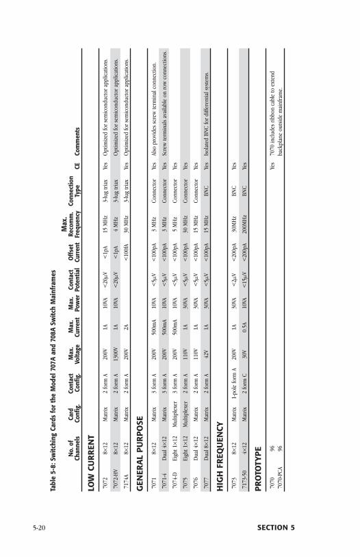
5-20 SECTION 5
Tabl
e5-
8:Sw
itchi
ngCa
rds
for
the
Mod
el70
7Aan
d70
8ASw
itch
Mai
nfra
mes
Max
.N
o.of
Card
Cont
act
Max
.M
ax.
Max
.Co
ntac
tO
ffse
tRe
com
m.
Conn
ectio
nCh
anne
lsCo
nfig.
Confi
g.Vo
ltage
Curr
ent
Pow
erPo
tent
ial
Curr
ent
Freq
uenc
yTy
peCE
Com
men
ts
LOW
CUR
REN
T
7072
8×12
Mat
rix2
form
A20
0V1A
10VA
<20
µV<
1pA
15M
Hz
3-lu
gtr
iax
Yes
Opt
imiz
edfo
rsem
icon
duct
orap
plic
atio
ns.
7072
-HV
8×12
Mat
rix2
form
A13
00V
1A10
VA<
20µV
<1p
A4
MH
z3-
lug
tria
xO
ptim
ized
fors
emic
ondu
ctor
appl
icat
ions
.
7174
A8×
12M
atrix
2fo
rmA
200V
2A<
100f
A30
MH
z3-
lug
tria
xYe
sO
ptim
ized
fors
emic
ondu
ctor
appl
icat
ions
.
GEN
ERA
LP
UR
POSE
7071
8×12
Mat
rix3
form
A20
0V50
0mA
10VA
<5µ
V<
100p
A3
MH
zCo
nnec
tor
Yes
Also
prov
ides
scre
wte
rmin
alco
nnec
tion.
7071
-4D
ual4
×12
Mat
rix3
form
A20
0V50
0mA
10VA
<5µ
V<
100p
A3
MH
zCo
nnec
tor
Yes
Scre
wte
rmin
als
avai
labl
eon
row
conn
ectio
ns.
7074
-DEi
ght1
×12
Mul
tiple
xer
3fo
rmA
200V
500m
A10
VA<
5µV
<10
0pA
5M
Hz
Conn
ecto
rYe
s
7075
Eigh
t1×1
2M
ultip
lexe
r2
form
A11
0V1A
30VA
<5µ
V<
100p
A30
MH
zCo
nnec
tor
Yes
7076
Dua
l4×1
2M
atrix
2fo
rmA
110V
1A30
VA<
5µV
<10
0pA
15M
Hz
Conn
ecto
rYe
s
7077
Dua
l8×1
2M
atrix
2fo
rmA
42V
1A30
VA<
5µV
<10
0pA
15M
Hz
BNC
Yes
Isol
ated
BNC
ford
iffer
entia
lsys
tem
s.
HIG
HFR
EQU
ENCY
7073
8×12
Mat
rix1-
pole
form
A20
0V1A
30VA
<2µ
V<
200p
A30
MH
zBN
CYe
s
7173
-50
4×12
Mat
rix2
form
C30
V0.
5A10
VA<
15µV
<20
0pA
200M
Hz
BNC
Yes
PR
OTO
TYP
E
7070
96Ye
s70
70in
clud
esrib
bon
cabl
eto
exte
nd70
70-P
CA96
back
plan
eou
tsid
em
ainf
ram
e.
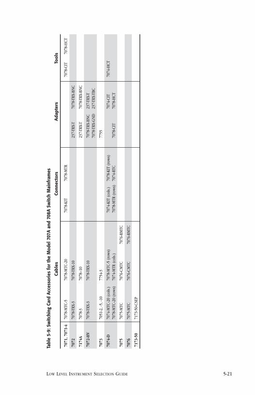
LOW LEVEL INSTRUMENT SELECTION GUIDE 5-21
Tabl
e5-
9:Sw
itchi
ngCa
rdAc
cess
orie
sfo
rth
eM
odel
707A
and
708A
Switc
hM
ainf
ram
es
Cabl
esCo
nnec
tors
Ada
pter
sTo
ols
7071
,707
1-4
7078
-MTC
-570
78-M
TC-2
070
78-K
IT70
78-M
TR70
78-C
IT70
78-H
CT
7072
7078
-TRX
-370
78-T
RX-1
023
7-TR
X-T
7078
-TRX
-BN
C
7174
A70
78-3
7078
--10
237-
TRX-
T70
78-T
RX-B
NC
7072
-HV
7078
-TRX
-370
78-T
RX-1
070
78-T
RX-B
NC
237-
TRX-
T70
78-T
RX-G
ND
237-
TRX-
TBC
7073
7051
-2,-
5,-1
077
54-3
7755
7074
-D70
74-M
TC-2
0(c
ols.)
7078
-MTC
-5(r
ows)
7074
-KIT
(col
s.)70
78-K
IT(r
ows)
7074
-CIT
7074
-HCT
7078
-MTC
-20
(row
s)70
74-M
TR(c
ols.)
7078
-MTR
(row
s)70
74-R
TC70
78-C
IT70
78-H
CT
7075
7075
-MTC
7076
-CM
TC70
76-R
MTC
7076
7075
-MTC
7076
-CM
TC70
76-R
MTC
7173
-50
7173
-50-
CSE
P
A P P E N D I X A
Low LevelMeasurement
Troubleshooting Guide
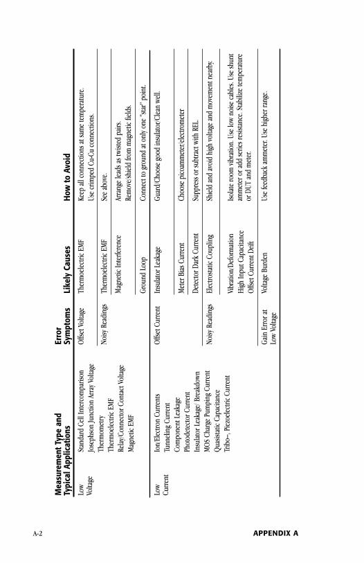
Mea
sure
men
tTyp
ean
dTy
pica
lApp
licat
ions
Erro
rSy
mpt
oms
Like
lyCa
uses
How
toAv
oid
Low
Volta
geSt
anda
rdCe
llIn
terc
ompa
rison
Jose
phso
nJu
nctio
nAr
rayV
olta
geTh
erm
omet
ryTh
erm
oele
ctric
EMF
Relay
/Con
nect
orCo
ntac
tVol
tage
Mag
netic
EMF
Offse
tVol
tage
Ther
moe
lectri
cEM
FKe
epall
conn
ectio
nsat
sam
ete
mpe
ratu
re.
Use
crim
ped
Cu-C
uco
nnec
tions
.
Noisy
Read
ings
Ther
moe
lectri
cEM
FSe
eabo
ve.
Mag
netic
Inte
rfere
nce
Arra
nge
leads
astw
isted
pairs
.Re
mov
e/sh
ield
from
mag
netic
field
s.
Grou
ndLo
opCo
nnec
tto
grou
ndat
only
one
"sta
r"po
int.
Low
Curr
ent
Ion/
Elec
tron
Curre
nts
Tunn
elin
gCu
rrent
Com
pone
ntLe
akag
ePh
otod
etec
torC
urre
ntIn
sulat
orLe
akag
e/Br
eakd
own
MOS
Char
gePu
mpi
ngCu
rrent
Quas
istat
icCa
pacit
ance
Trib
o–,P
iezo
elec
tricC
urre
nt
Offse
tCur
rent
Insu
lator
Leak
age
Guar
d/Ch
oose
good
insu
lator
/Clea
nwe
ll.
Met
erBi
asCu
rrent
Choo
sepi
coam
met
er/el
ectro
met
er
Dete
ctorD
ark
Curre
ntSu
ppre
ssor
subt
ract
with
REL.
Noisy
Read
ings
Elec
trosta
ticCo
uplin
gSh
ield
and
avoi
dhi
ghvo
ltage
and
mov
emen
tnea
rby.
Vibr
atio
n/De
form
atio
nHi
ghIn
putC
apac
itanc
eOf
fsetC
urre
ntDr
ift
Isolat
ero
omvib
ratio
n.Us
elo
wno
iseca
bles
.Use
shun
tam
met
eror
add
serie
sres
istan
ce.S
tabi
lize
tem
pera
ture
orDU
Tan
dm
eter
.
Gain
Erro
rat
Low
Volta
geVo
ltage
Burd
enUs
efe
edba
ckam
met
er.U
sehi
gher
rang
e.
A-2 APPENDIX A
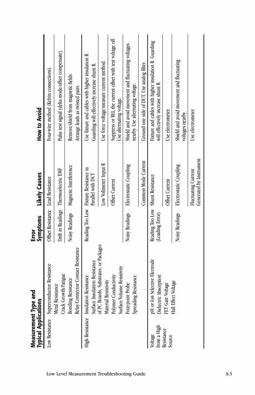
Mea
sure
men
tTyp
ean
dTy
pica
lApp
licat
ions
Erro
rSy
mpt
oms
Like
lyCa
uses
How
toAv
oid
Low
Resis
tanc
eSu
perc
ondu
ctorR
esist
ance
Met
alRe
sista
nce
Crac
kGr
owth
/Fat
igue
Bond
ing
Resis
tanc
eRe
lay/C
onne
ctorC
onta
ctRe
sista
nce
Offse
tRes
istan
ceLe
adRe
sistan
ceFo
ur-w
irem
etho
d(K
elvin
conn
ectio
ns).
Drift
inRe
adin
gsTh
erm
oelec
tricE
MF
Pulse
test
signa
l(de
ltam
ode/
offse
tcom
pens
ate).
Noisy
Read
ings
Mag
netic
Inte
rfere
nce
Rem
ove/
shiel
dfro
mm
agne
ticfie
lds.
Arra
nge
leads
astw
isted
pairs
.
High
Resis
tanc
eIn
sulat
ion
Resis
tanc
eSu
rface
Insu
latio
nRe
sista
nce
ofPC
Boar
ds,S
ubstr
ates
,orP
acka
ges
Mat
erial
Resis
tivity
Polym
erCo
nduc
tivity
Surfa
ce/V
olum
eRe
sistiv
ityFo
ur-p
oint
Prob
eSp
read
ing
Resis
tanc
e
Read
ing
Too
Low
Fixt
ure
Resis
tanc
ein
Para
llelw
ithDU
TUs
efix
ture
and
cabl
eswi
thhi
gher
insu
latio
nR.
Guar
ding
will
effe
ctive
lyin
crea
sesh
untR
.
Low
Voltm
eter
Inpu
tRUs
efo
rce
volta
ge/m
easu
recu
rrent
met
hod.
Offse
tCur
rent
Supp
ress
orRE
Lth
ecu
rrent
offse
twith
test
volta
geof
f.Us
ealt
erna
ting
volta
ge.
Noisy
Read
ings
Elec
trosta
ticCo
uplin
gSh
ield
and
avoi
dm
ovem
enta
ndflu
ctuat
ing
volta
ges
near
by.U
sealt
erna
ting
volta
ge.
Com
mon
Mod
eCu
rrent
Grou
ndon
esid
eof
DUT.
Use
analo
gfil
ter.
Volta
gefro
ma
High
Resis
tanc
eSo
urce
pHor
Ion
Sele
ctive
Elec
trode
Diel
ectri
cAbs
orpt
ion
FET
Gate
Volta
geHa
llEf
fect
Volta
ge
Read
ing
Too
Low
(Loa
ding
Erro
r)Sh
untR
esist
ance
Fixt
ure
and
cabl
eswi
thhi
gher
insu
latio
nR.
Guar
ding
will
effe
ctive
lyin
crea
sesh
untR
.
Offse
tCur
rent
Usee
lectro
met
er.
Noisy
Read
ings
Elec
trosta
ticCo
uplin
gSh
ield
and
avoi
dm
ovem
enta
ndflu
ctuati
ngvo
ltage
snea
rby.
Fluc
tuat
ing
Curre
ntGe
nera
ted
byIn
strum
ent
Use
electr
omet
er.
Low Level Measurement Troubleshooting Guide A-3
A P P E N D I X B
Cable andConnectorAssembly
B-2 APPENDIX B
Proper cable and connector assembly is an important factor in maintainingthe integrity of low level measurements. Generally, three types of cable areused with low level instruments: coaxial, triaxial, and shielded twisted pair.In addition, the cable is often of low noise or low thermoelectric EMFdesign. To prepare a low noise coaxial or triaxial cable for either direct con-nection to a source or for connector assembly, follow the steps illustrated inFigure B-1:
1. Gently cut through outer insulation without cutting the shield.
2. Using a sharp point, unravel the shield braid.
3. Twist the braid and thoroughly clean off all traces of graphite withmethanol. For triax cable, repeat the previous steps with the innershield.
4. Cut center conductor to proper length, strip insulation off center con-ductor, and “tin” leads.
5. For insertion into connectors, the braid is cut back in accordance withthe assembly instructions for the particular connector type.
Connectors should have high resistance insulation. Teflon® is usuallypreferred because of its resistance to surface contaminants. Coaxial or tri-axial connectors are available with Teflon insulation.
Note that the BNC and two-slot triaxial connectors are very similar; takecare to ensure the connector is used only with a properly mating variety. IfBNC and two-slot triax connectors are mated, the result will be permanentdamage to the plug and receptacle. Using three-slot triaxial connectorswhere appropriate will eliminate this problem.
While some low level instruments use coaxial connections, most use tri-axial connectors. Triaxial cable provides the grounded shielding necessaryfor high common-mode measurements; generally, the outer shield is con-nected to power-line ground, while the inner shield is connected to signalLO. Also, triaxial connections make it easy to use guarding. In this configura-tion, the inner shield is connected to guard potential, and the outer shieldis connected to ground. Safety hazards can exist when using this scheme insituations where exposed metal is at guard potential and the guard voltageis above 30Vrms.
As with any insulated device, connector insulation must be kept clean toavoid reducing its leakage resistance. Avoid touching insulating material. Ifthe connector becomes contaminated, it can be cleaned with methanol ordistilled water. When cleaning, use only the purest cleaning agents and thor-oughly flush contaminants away from the affected area. After all contami-nants are removed, allow the connector to dry for several hours in a lowhumidity environment before use.
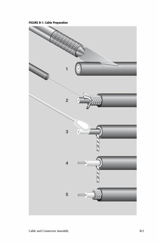
Cable and Connector Assembly B-3
1
2
3
4
5
FIGURE B-1: Cable Preparation

A P P E N D I X C
Glossary
C-2 APPENDIX C
ABSOLUTE ACCURACY. A measure of the closeness of agreement of an instru-ment reading compared to that of a primary standard having absolutetraceability to a standard sanctioned by a recognized standards organi-zation. Accuracy is often separated into gain and offset terms. See alsoRELATIVE ACCURACY.
A/D (ANALOG-TO-DIGITAL) CONVERTER. A circuit used to convert an analoginput signal into digital information. All digital meters use an A/D con-verter to convert the input signal into digital information.
ANALOG OUTPUT. An output that is directly proportional to the input signal.
ASSEMBLER. A molecular manufacturing device that can be used to guidechemical reactions by positioning molecules. An assembler can be pro-grammed to build virtually any molecular structure or device from sim-pler chemical building blocks.
AUTO-RANGING. The ability of an instrument to automatically switch amongranges to determine the range offering the highest resolution. Theranges are usually in decade steps.
AUTO-RANGING TIME. For instruments with auto-ranging capability, the timeinterval between application of a step input signal and its display, includ-ing the time for determining and changing to the correct range.
BANDWIDTH. The range of frequencies that can be conducted or amplifiedwithin certain limits. Bandwidth is usually specified by the –3dB (half-power) points.
BIAS VOLTAGE. A voltage applied to a circuit or device to establish a referencelevel or operating point of the device during testing.
CAPACITANCE. In a capacitor or system of conductors and dielectrics, thatproperty which permits the storage of electrically separated chargeswhen potential differences exist between the conductors. Capacitance isrelated to the charge and voltage as follows: C = Q/V, where C is thecapacitance in farads, Q is the charge in coulombs, and V is the voltagein volts.
CARBON NANOTUBE. A tube-shaped nanodevice formed from a sheet of single-layer carbon atoms that has novel electrical and tensile properties.These fibers may exhibit electrical conductivity as high as copper, ther-mal conductivity as high as diamond, strength 100 times greater thansteel at one-sixth of steel’s weight, and high strain to failure. They canbe superconducting, insulating, semiconducting, or conducting (metal-lic). Non-carbon nanotubes, often called nanowires, are often createdfrom boron nitride or silicon.
CHANNEL (SWITCHING). One of several signal paths on a switching card. Forscanner or multiplexer cards, the channel is used as a switched input inmeasuring circuits, or as a switched output in sourcing circuits. Forswitch cards, each channel’s signals paths are independent of other
Glossary C-3
channels. For matrix cards, a channel is established by the actuation ofa relay at a row and column crosspoint.
COAXIAL CABLE. A cable formed from two or more coaxial cylindrical con-ductors insulated from each other. The outermost conductor is oftenearth grounded.
COMMON-MODE REJECTION RATIO (CMRR). The ability of an instrument toreject interference from a common voltage at its input terminals withrespect to ground. Usually expressed in decibels at a given frequency.
COMMON-MODE CURRENT. The current that flows between the input low ter-minal and chassis ground of an instrument.
COMMON-MODE VOLTAGE. A voltage between input low and earth ground ofan instrument.
CONTACT RESISTANCE. The resistance in ohms between the contacts of a relayor connector when the contacts are closed or in contact.
CONTAMINATION. Generally used to describe the unwanted material thatadversely affects the physical, chemical, or electrical properties of asemiconductor or insulator.
D/A (DIGITAL-TO-ANALOG) CONVERTER. A circuit used to convert digital infor-mation into an analog signal. D/A converters are used in many instru-ments to provide an isolated analog output.
DIELECTRIC ABSORPTION. The effect of residual charge storage after a previ-ously charged capacitor has been discharged momentarily.
DIGITAL MULTIMETER (DMM). An electronic instrument that measures voltage,current, resistance, or other electrical parameters by converting the ana-log signal to digital information and display. The typical five-functionDMM measures DC volts, DC amps, AC volts, AC amps, and resistance.
DRIFT. A gradual change of a reading with no change in input signal or oper-ating conditions.
DRY CIRCUIT TESTING. The process of measuring a device while keeping thevoltage across the device below a certain level (e.g., <20mV) in order toprevent disturbance of oxidation or other degradation of the devicebeing measured.
ELECTROCHEMICAL EFFECT. A phenomenon whereby currents are generated bygalvanic battery action caused by contamination and humidity.
ELECTROMETER. A highly refined DC multimeter. In comparison with a digi-tal multimeter, an electrometer is characterized by higher input resist-ance and greater current sensitivity. It can also have functions notgenerally available on DMMs (e.g., measuring electric charge, sourcingvoltage).
EMF. Electromotive force or voltage. EMF is generally used in context of avoltage difference caused by electromagnetic, electrochemical, or ther-mal effects.
C-4 APPENDIX C
ELECTROSTATIC COUPLING. A phenomenon whereby a current is generated bya varying or moving voltage source near a conductor.
ERROR. The deviation (difference or ratio) of a measurement from its truevalue. True values are by their nature indeterminate. See also RANDOM
ERROR and SYSTEMATIC ERROR.
FALL TIME. The time required for a signal to change from a large percentage(usually 90%) to a small percentage (usually 10%) of its peak-to-peakvalue. See also RISE TIME.
FARADAY CUP. A Faraday cup (sometimes called a Faraday cage or icepail) isan enclosure made of sheet metal or mesh. It consists of two electrodes,one inside the other, separated by an insulator. While the inner elec-trode is connected to the electrometer, the outer electrode is connect-ed to ground. When a charged object is placed inside the inner elec-trode, all the charge will flow into themeasurement instrument. Theelectric field inside a closed, empty conductor is zero, so the cup shieldsthe object placed inside it from any atmospheric or stray electric fields.This allows measuring the charge on the object accurately.
FEEDBACK PICOAMMETER. A sensitive ammeter that uses an operationalamplifier feedback configuration to convert an input current into volt-age for measurement.
FLOATING. The condition where a common-mode voltage exists between anearth ground and the instrument or circuit of interest. (Circuit low is nottied to earth potential.)
FOUR-POINT PROBE. The four-point collinear probe resistivity measurementtechnique involves bringing four equally spaced probes in contact withthe material of unknown resistance. The array is placed in the center ofthe material. A known current is passed through the two outside probesand the voltage is sensed at the two inside probes. The resistivity is cal-culated as follows:
π Vρ = —— × — × t × k
ln2 I
where: V = the measured voltage in volts, I = the source current inamps, t = the wafer thickness in centimeters, k = a correction factorbased on the ratio of the probe to wafer diameter and on the ratio ofwafer thickness to probe separation.
FOUR-TERMINAL RESISTANCE MEASUREMENT. A measurement where two leads areused to supply a current to the unknown, and two different leads areused to sense the voltage drop across the resistance. The four-terminalconfiguration provides maximum benefits when measuring low resist-ances.
FULLERENE. Refers to C60, an approximately spherical, hollow, carbon mol-ecule containing 60 carbon atoms arranged in interlocking hexagonsand pentagons, reminiscent of the geodesic dome created by architect
Glossary C-5
R. Buckminster Fuller. Sometimes called “buckminsterfullerene” or“buckyball.”
GROUND LOOP. A situation resulting when two or more instruments are con-nected to different points on the ground bus and to earth or power lineground. Ground loops can develop undesired offset voltages or noise.
GUARDING. A technique that reduces leakage errors and decreases responsetime. Guarding consists of a conductor driven by a low impedancesource surrounding the lead of a high impedance signal. The guard volt-age is kept at or near the potential of the signal voltage.
HALL EFFECT. The measurement of the transverse voltage across a conductorwhen placed in a magnetic field. With this measurement, it is possible todetermine the type, concentration, and mobility of carriers in silicon.
HIGH IMPEDANCE TERMINAL. A terminal where the source resistance times theexpected stray current (for example, 1µA) exceeds the required voltagemeasurement sensitivity.
INPUT BIAS CURRENT. The current that flows at the instrument input due tointernal instrument circuitry and bias voltage.
INPUT IMPEDANCE. The shunt resistance and capacitance (or inductance) asmeasured at the input terminals, not including effects of input bias oroffset currents.
INPUT OFFSET CURRENT. The difference between the two currents that mustbe supplied to the input measuring terminals of a differential instru-ment to reduce the output indication to zero (with zero input voltageand offset voltage). Sometimes informally used to refer to input biascurrent.
INPUT OFFSET VOLTAGE. The voltage that must be applied directly between theinput measuring terminals, with bias current supplied by a resistancepath, to reduce the output indication to zero.
INPUT RESISTANCE. The resistive component of input impedance.
INSULATION RESISTANCE. The ohmic resistance of insulation. Insulation resist-ance degrades quickly as humidity increases.
JOHNSON NOISE. The noise in a resistor caused by the thermal motion ofcharge carriers. It has a white noise spectrum and is determined by thetemperature, bandwidth, and resistance value.
LEAKAGE CURRENT. Error current that flows (leaks) through insulation resist-ance when a voltage is applied. Even high resistance paths between lowcurrent conductors and nearby voltage sources can generate significantleakage currents.
LONG-TERM ACCURACY. The limit that errors will not exceed during a 90-dayor longer time period. It is expressed as a percentage of reading (orsourced value) plus a number of counts over a specified temperaturerange.
C-6 APPENDIX C
MAXIMUM ALLOWABLE INPUT. The maximum DC plus peak AC value (voltage orcurrent) that can be applied between the high and low input measuringterminals without damaging the instrument.
MEMS. Microelectromechanical systems. Describes systems that can re-spond to a stimulus or create physical forces (sensors and actuators) andthat have dimensions on the micrometer scale. They are typically manu-factured using the same lithographic techniques used to make silicon-based ICs.
MICRO-OHMMETER. An ohmmeter that is optimized for low resistance meas-urements. The typical micro-ohmmeter uses the four-terminal measure-ment method and has special features for optimum low level measure-ment accuracy.
MOLECULAR ELECTRONICS. Any system with atomically precise electronicdevices of nanometer dimensions, especially if made of discrete molec-ular parts, rather than the continuous materials found in today’s semi-conductor devices.
MOLECULAR MANIPULATOR. A device combining a proximal-probe mechanismfor atomically precise positioning with a molecule binding site on thetip; can serve as the basis for building complex structures by positionalsynthesis.
MOLECULAR MANUFACTURING. Manufacturing using molecular machinery,giving molecule-by-molecule control of products and by-products viapositional chemical synthesis.
MOLECULAR NANOTECHNOLOGY. Thorough, inexpensive control of the struc-ture of matter based on molecule-by-molecule control of products andby-products; the products and processes of molecular manufacturing,including molecular machinery.
MOSFET. A metal oxide field effect transistor. A unipolar device character-ized by extremely high input resistance.
NANO-. A prefix meaning one billionth (1/1,000,000,000).
NANOELECTRONICS. Electronics on a nanometer scale. Includes both molecu-lar electronics and nanoscale devices that resemble current semicon-ductor devices.
NANOTECHNOLOGY. Fabrication of devices with atomic or molecular scale pre-cision. Devices with minimum feature sizes less than 100 nanometers(nm) are considered products of nanotechnology. A nanometer [one-billionth of a meter (10–9m)] is the unit of length generally most appro-priate for describing the size of single molecules.
NANOVOLTMETER. A voltmeter optimized to provide nanovolt sensitivity (gen-erally uses low thermoelectric EMF connectors, offset compensation,etc.).
NOISE. Any unwanted signal imposed on a desired signal.
Glossary C-7
NORMAL-MODE REJECTION RATIO (NMRR). The ability of an instrument to rejectinterference across its input terminals. Usually expressed in decibels ata specific frequency such as that of the AC power line.
NORMAL-MODE VOLTAGE. A voltage applied between the high and low inputterminals of an instrument.
OFFSET CURRENT. A current generated by a circuit even though no signals areapplied. Offset currents are generated by triboelectric, piezoelectric, orelectrochemical effects present in the circuit.
OVERLOAD PROTECTION. A circuit that protects the instrument from excessivecurrent or voltage at the input terminals.
PICOAMMETER. An ammeter optimized for the precise measurement of smallcurrents. Generally, a feedback ammeter.
PIEZOELECTRIC EFFECT. A term used to describe currents generated whenmechanical stress is applied to certain types of insulators.
PRECISION. Refers to the freedom of uncertainty in the measurement. It isoften applied in the context of repeatability or reproducibility andshould not be used in place of accuracy. See also UNCERTAINTY.
QUANTUM DOT. A nanoscale object (usually a semiconductor island) that canconfine a single electron (or a few) and in which the electrons occupydiscrete energy states, just as they would in an atom. Quantum dotshave been called “artificial atoms.”
RANDOM ERROR. The mean of a large number of measurements influenced byrandom error matches the true value. See also SYSTEMATIC ERROR.
RANGE. A continuous band of signal values that can be measured orsourced. In bipolar instruments, range includes positive and negativevalues.
READING. The displayed number that represents the characteristic of theinput signal.
READING RATE. The rate at which the reading number is updated. The read-ing rate is the reciprocal of the time between readings.
RELATIVE ACCURACY. The accuracy of a measuring instrument in reference toa secondary standard. See also ABSOLUTE ACCURACY.
REPEATABILITY. The closeness of agreement between successive measure-ments carried out under the same conditions.
REPRODUCIBILITY. The closeness of agreement between measurements of thesame quantity carried out with a stated change in conditions.
RESOLUTION. The smallest portion of the input (or output) signal that can bemeasured (or sourced) and displayed.
RESPONSE TIME. For a measuring instrument, the time between applicationof a step input signal and the indication of its magnitude within a ratedaccuracy. For a sourcing instrument, the time between a programmed
C-8 APPENDIX C
change and the availability of the value at its output terminals. Alsoknown as SETTLING TIME.
RISE TIME. The time required for a signal to change from a small percentage(usually 10%) to a large percentage (usually 90%) of its peak-to-peakamplitude. See also FALL TIME.
SENSITIVITY. The smallest quantity that can be measured and displayed.
SETTLING TIME. For a measuring instrument, the time between application ofa step input signal and the indication of its magnitude within a ratedaccuracy. For a sourcing instrument, the time between a programmedchange and the availability of the value at its output terminals. Alsoknown as RESPONSE TIME.
SHIELDING. A metal enclosure around the circuit being measured, or a metalsleeve surrounding the wire conductors (coax or triax cable) to lesseninterference, interaction, or leakage. The shield is usually grounded orconnected to input LO.
SHUNT AMMETER. A type of ammeter that measures current by converting theinput current into a voltage by means of shunt resistance. Shunt amme-ters have higher voltage burden and lower sensitivity than do feedbackammeters.
SHUNT CAPACITANCE LOADING. The effect on a measurement of the capacitanceacross the input terminals, such as from cables or fixtures. Shunt capac-itance increases both rise time and settling time.
SHORT-TERM ACCURACY. The limit that errors will not exceed during a short,specified time period (such as 24 hours) of continuous operation.Unless specified, no zeroing or adjustment of any kind are permitted. Itis expressed as percentage of reading (or sourced value) plus a numberof counts over a specified temperature range.
SINGLE ELECTRON TRANSISTOR. A switching device that uses controlled elec-tron tunneling to amplify current. An SET is made from two tunnel junc-tions that share a common electrode. A tunnel junction consists of twopieces of metal separated by a very thin (~1nm) insulator. The only wayfor electrons in one of the metal electrodes to travel to the other elec-trode is to tunnel through the insulator. Tunneling is a discrete process,so the electric charge that flows through the tunnel junction flows inmultiples of e, the charge of a single electron.
SOURCE IMPEDANCE. The combination of resistance and capacitive or induc-tive reactance the source presents to the input terminals of a measuringinstrument.
SOURCE-MEASURE UNIT (SMU). An electronic instrument that sources andmeasures DC voltage and current. Generally, SMUs have two modes ofoperation: source voltage and measure current, or source current andmeasure voltage. Also known as source-monitor unit or stimulus-measurement unit.
Glossary C-9
SOURCEMETER. A SourceMeter instrument is very similar to the source-measure unit in many ways, including its ability to source and measureboth current and voltage and to perform sweeps. In addition, aSourceMeter instrument can display the measurements directly in resist-ance, as well as voltage and current. It is designed for general-purpose,high speed production test applications. It can also be used as a sourcefor moderate to low level measurements and for research applications.
SOURCE RESISTANCE. The resistive component of source impedance. See alsoTHEVENIN EQUIVALENT CIRCUIT.
SPINTRONICS. Electronics that take advantage of the spin of an electron insome way, rather than just its charge.
STANDARD CELL. An electrochemical cell used as a voltage reference in labo-ratories.
SUPERCONDUCTOR. A conductor that has zero resistance. Such materials usu-ally become superconducting only at very low temperatures.
SWITCH CARD. A type of card with independent and isolated relays forswitching inputs and outputs on each channel.
SWITCHING MAINFRAME. A switching instrument that connects signals amongsourcing and measuring instruments and devices under test. A main-frame is also referred to as a scanner, multiplexer, matrix, or program-mable switch.
SYSTEMATIC ERROR. The mean of a large number of measurements influencedby systematic error deviates from the true value. See also RANDOM ERROR.
TEMPERATURE COEFFICIENT. A measure of the change in reading (or sourcedvalue) with a change in temperature. It is expressed as a percentage ofreading (or sourced value), plus a number of counts per degree changein temperature.
TEMPERATURE COEFFICIENT OF RESISTANCE. The change of resistance of a mater-ial or device per degree of temperature change, usually expressed inppm/°C.
THERMOELECTRIC EMFS. Voltages resulting from temperature differenceswithin a measuring circuit or when conductors of dissimilar materialsare joined together.
THEVENIN EQUIVALENT CIRCUIT. A circuit used to simplify analysis of complex,two-terminal linear networks. The Thevenin equivalent voltage is theopen-circuit voltage and the Thevenin equivalent resistance equals theopen-circuit voltage divided by the short-circuit current.
TRANSFER ACCURACY. A comparison of two nearly equal measurements over alimited temperature range and time period. It is expressed in ppm. Seealso RELATIVE ACCURACY, SHORT-TERM ACCURACY.
TRIBOELECTRIC EFFECT. A phenomenon whereby currents are generated bycharges created by friction between a conductor and an insulator.
C-10 APPENDIX C
TRIGGER. An external stimulus that initiates one or more instrument func-tions. Trigger stimuli include: an input signal, the front panel, an exter-nal trigger pulse, and IEEE-488 bus X, talk, and GET triggers.
TWO-TERMINAL RESISTANCE MEASUREMENT. A measurement where the sourcecurrent and sense voltage are applied through the same set of test leads.
UNCERTAINTY. An estimate of the possible error in a measurement; in otherwords, the estimated possible deviation from its actual value.
VAN DER PAUW MEASUREMENT. A measurement technique used to measure theresistivity of arbitrarily shaped samples.
VOLTAGE BURDEN. The voltage drop across the input terminals of anammeter.
VOLTAGE COEFFICIENT. The change in resistance value with applied voltage.Usually expressed in percent/V or in ppm/V.
WARM-UP TIME. The time required after power is applied to an instrument toachieve rated accuracy at reference conditions.
ZERO OFFSET. The reading that occurs when the input terminals of a meas-uring instrument are shorted (voltmeter) or open-circuited (ammeter).
A P P E N D I X D
SafetyConsiderations

Test System SafetyMany electrical test systems or instruments are capable of measuring orsourcing hazardous voltage and power levels. It is also possible, under sin-gle fault conditions (e.g., a programming error or an instrument failure), tooutput hazardous levels even when the system indicates no hazard is pre-sent.
These high voltage and power levels make it essential to protect operatorsfrom any of these hazards at all times.
Protection methods include:
• Design test fixtures to prevent operator contact with any hazardouscircuit.
• Make sure the device under test is fully enclosed to protect the operator from any flying debris.
• Double insulate all electrical connections that an operator couldtouch. Double insulation ensures the operator is still protected, evenif one insulation layer fails.
• Use high-reliability, fail-safe interlock switches to disconnect powersources when a test fixture cover is opened.
• Where possible, use automated handlers so operators do not requireaccess to the inside of the test fixture or have a need to open guards.
• Provide proper training to all users of the system so they understand all potential hazards and know how to protect themselves frominjury.
CAUTION: During power-up, the states of board outputs are uncontrolleduntil hardware and software initialization has been completed. Users mustmake sure their designs can tolerate this or provide suitable interlocks toprevent dangerous voltages or actions from reaching users.
General Safety ConsiderationsIt is the responsibility of the test system designers, integrators, and installersto make sure operator and maintenance personnel protection is in placeand effective.
The following safety precautions should be observed before using anyKeithley product and any associated instrumentation. Although someinstruments and accessories would normally be used with non-hazardous voltages, there are situations where hazardous conditions may bepresent. Keithley products are intended for use by qualified personnel whorecognize shock hazards and are familiar with the safety precautionsrequired to avoid possible injury. Read the operating information providedin each product's manual carefully before using any Keithley product.
D-2 APPENDIX DD-2 APPENDIX D
The types of product users are:
Responsible body is the individual or group responsible for the use andmaintenance of equipment, for ensuring that the equipment is operatedwithin its specifications and operating limits, and for ensuring that opera-tors are adequately trained.
Operators use the product for its intended function. They must be trainedin electrical safety procedures and proper use of the instrument. They mustbe protected from electric shock and contact with hazardous live circuits.
Maintenance personnel perform routine procedures on the product tokeep it operating, for example, setting the line voltage or replacing con-sumable materials. Maintenance procedures are described in the manual.The procedures explicitly state if the operator may perform them.Otherwise, they should be performed only by service personnel.
Service personnel are trained to work on live circuits, and perform safeinstallations and repairs of products. Only properly trained service person-nel may perform installation and service procedures.
Exercise extreme caution when a shock hazard is present. Lethal voltagemay be present on cable connector jacks or test fixtures. The AmericanNational Standards Institute (ANSI) states that a shock hazard exists whenvoltage levels greater than 30V RMS, 42.4V peak, or 60VDC are present. Agood safety practice is to expect that hazardous voltage is present in anyunknown circuit before measuring.
Users of these products must be protected from electric shock at all times.The responsible body must ensure that users are prevented access and/orinsulated from every connection point. In some cases, connections must beexposed to potential human contact. Product users in these circumstancesmust be trained to protect themselves from the risk of electric shock. If thecircuit is capable of operating at or above 1000 volts, no conductive part ofthe circuit may be exposed.
As described in the International Electrotechnical Commission (IEC)Standard IEC 664, these instruments are Installation Category I, and signallines must not be directly connected to AC mains.
For rack mounted equipment in which the power cord is not accessible, inthe event of fire or other catastrophic failure, the user must provide a sepa-rate power disconnect switch.
Do not connect switching cards directly to unlimited power circuits. Theyare intended to be used with impedance limited sources. NEVER connectswitching cards directly to AC mains. When connecting sources to switchingcards, install protective devices to limit fault current and voltage to the card.
Before operating an instrument, make sure the line cord is connected to aproperly grounded power receptacle. Inspect the connecting cables, testleads, and jumpers for possible wear, cracks, or breaks before each use.
Safety Considerations D-3
D-4 APPENDIX DD-4 APPENDIX D
For maximum safety, do not touch the product, test cables, or any otherinstruments while power is applied to the circuit under test. ALWAYSremove power from the entire test system and discharge any capacitorsbefore: connecting or disconnecting cables or jumpers, installing or remov-ing switching cards, or making internal changes, such as installing or remov-ing jumpers.
Do not touch any object that could provide a current path to the commonside of the circuit under test or power line (earth) ground. Always makemeasurements with dry hands while standing on a dry, insulated surfacecapable of withstanding the voltage being measured.
Instruments and accessories must be used in accordance with specificationsand operating instructions or the safety of the equipment may be impaired.
Do not exceed the maximum signal levels of the instruments and acces-sories, as defined in the specifications and operating information, and asshown on the instrument or test fixture panels, or switching card.
When fuses are used in a product, replace with same type and rating forcontinued protection against fire hazard.
Chassis connections must only be used as shield connections for measuring circuits, NOT as safety earth ground connections.
If you are using a test fixture, keep the lid closed while power is applied tothe device under test. Safe operation requires the use of a lid interlock.
If a screw is present, connect it to safety earth ground using the wirerecommended in the user documentation.
The symbol on an instrument indicates that the user should refer tothe operating instructions located in the manual.
The symbol on an instrument shows that it can source or measure1000 volts or more, including the combined effect of normal and common mode voltages. Use standard safety precautions to avoid personal contact with these voltages.
The WARNING heading in a manual explains dangers that might result inpersonal injury or death. Always read the associated information very care-fully before performing the indicated procedure.
The CAUTION heading in a manual explains hazards that could damage theinstrument. Such damage may invalidate the warranty.
Instrumentation and accessories shall not be connected to humans.
Before performing any maintenance, disconnect the line cord and all testcables.
To maintain protection from electric shock and fire, replacement compo-nents in mains circuits, including the power transformer, test leads, andinput jacks, must be purchased from Keithley Instruments. Standard fuses,with applicable national safety approvals, may be used if the rating and type
are the same. Other components that are not safety related may be pur-chased from other suppliers as long as they are equivalent to the originalcomponent. (Note that selected parts should be purchased only throughKeithley Instruments to maintain accuracy and functionality of the product.)If you are unsure about the applicability of a replacement component, calla Keithley Instruments office for information.
To clean an instrument, use a damp cloth or mild, water based cleaner.Clean the exterior of the instrument only. Do not apply cleaner directly tothe instrument or allow liquids to enter or spill on the instrument. Productsthat consist of a circuit board with no case or chassis (e.g., data acquisitionboard for installation into a computer) should never require cleaning if han-dled according to instructions. If the board becomes contaminated andoperation is affected, the board should be returned to the factory for prop-er cleaning/servicing.
Safety Considerations D-5
INDEX
I-2 INDEX
1/f noise, 3-7 to 3-83dB point, 2-53
Absolute accuracy, 1-10, 1-12AC interference and damping, 2-31 to
2-23AC pickup, 3-24Accuracy, 1-10 to 1-13Alternating polarity technique
(resistivity measurements), 4-25 to4-26
Alternating voltage method (resistivitymeasurements), 4-26
Ammeter, 1-17 to 1-21Analog outputs, 2-66Avalanche photodiode (APD), 4-18 to
4-19
Bandwidth, 2-53 to 2-54
Cabling, 2-26Capacitance measurements, 4-37 to
4-38Capacitors
dielectric absorptionmeasurements, 4-2 to 4-5
leakage measurements, 4-9 to 4-11Ceramic insulators, 2-12 to 2-13, 2-23Charge measurements, 1-7, 1-22, 2-33,
2-44 to 2-47, 4-36 to 4-39Circuit design basics, 1-16 to 1-33Common-mode current errors, 3-15 to
3-16, 4-31 to 4-32Common-mode rejection ratio (CMRR),
1-14 to 1-15Conductivity measurements, 4-8Connections
BNC connectors, 2-63 to 2-64cables, 2-62 to 2-63instrument to DUT, 2-47 to 2-49prevention of thermoelectric
EMFs, 3-5triax cabling and connectors, 2-64
to 2-65Constant-current method (resistance
measurement), 1-6, 2-37 to 2-43,2-58
Constant-voltage method (resistancemeasurement), 1-6, 2-36 to 2-37
Contact resistance, 4-44 to 4-47Contamination, 2-14, 2-24, 2-26 to 2-28,
2-44Coulombmeter, 1-7, 1-22
for charge measurements, 4-36for current measurements, 2-33 to
2-36Cryogenic temperatures, 3-5, 3-11Current measurements
low, 4-9 to 4-19semiconductor, 4-11 to 4-13
Current noise, 2-62Current-reversal method (for canceling
thermoelectric EMFs), 3-19 to 3-20, see also Source reversal
Damping, 2-31 to 2-32Dark current, 4-16Delta method (for canceling
thermoelectric EMFs), 3-20 to 3-22, 4-49
Deratings, 1-13 to 1-14Device heating, 3-24Dielectric absorption, 2-11 to 2-12,
2-28, 4-2 to 4-5Digital multimeter (DMM), 1-3, 1-7,
1-29 to 1-30, 3-24Dry circuit testing, 1-9, 1-27 to 1-28,
3-25 to 3-26, 4-45 to 4-46
Electrochemical effects (currentgeneration), 2-23, 2-26 to 2-28
Electrochemical measurements, 4-5 to4-8
Electrometerapplications
capacitor leakagemeasurements, 4-9 to 4-11
charge measurements, 4-36to 4-39
conductivity measurements,4-8
determining dielectricabsorption, 4-2 to 4-5
Low Level Measurements Handbook I-3
high resistancemeasurements, 4-20 to4-36
low current semiconductormeasurements, 4-11 to 4-13
pH measurements, 4-5 to 4-7
description, 1-5 to 1-7, 1-29general measurement
considerations, 2-47 to 2-68measurement verification
techniques, 2-68Electromagnetic interference (EMI), 3-6
to 3-9Electrostatic coupling/interference, 2-49
to 2-52Error, 1-10, 3-2 to 3-10
calculating from instrumentspecifications, 1-13
common-mode current errors, 3-15 to 3-16, 4-31 to 4-32
random, 1-10External offset current, 2-24 to 2-25
Faraday cup, 4-38 to 4-39Feedback ammeter, 1-18 to 1-19, 2-14,
2-20 to 2-21, 2-56 to 2-57Filtering (device input paths to prevent
RFI), 3-8Floating input signals, 2-67 to 2-68Four-point collinear probe resistivity
measurement technique, 4-26 to4-29, 4-51
Four-wire measurements, 1-9, 2-39 to 2-40
FrequencyAC signals, 2-53voltage noise, 3-6 to 3-8
Generated currents, 2-45Glass epoxy insulators, 2-12 to 2-13Ground loops, 3-13 to 3-15Guarding, 2-6 to 2-10, 2-14 to 2-19,
2-40 to 2-41, 2-42, 2-51 to 2-52
High megohm resistors, 2-43 to 2-44Humidity, 2-15, 2-26 to 2-28, 2-44, 2-52
Inductive devices, 3-26 to 3-27Input burden, 1-4 to 1-5Input offset current, 1-4, 2-14, 2-22 to
2-24, 2-44Instrument response speed, 2-53 to
2-58Insulation resistance, 2-11 to 2-14, 2-27
to 2-28Insulator handling and cleaning, 2-14,
2-24, 2-28Ion beam measurements, 4-16 to 4-18Ionization interference, 2-53Ion-selective electrodes, 4-5 to 4-7
Johnson noise, 2-36, 2-58 to 2-62, 3-10to 3-11
Kel-F® insulators, 2-12 to 2-13
Lead resistance, 3-16 to 3-19Leakage current, 1-4, 2-14 to 2-19, 4-12Leakage resistance, 1-4Light interference, 2-52Light measurements, 4-14 to 4-16Loading errors, 2-2 to 2-10Lucite® insulators, 2-14
Magnetic fields and error voltagegeneration, 3-11 to 3-13
Measurement speed, 1-15Microcalorimetry, 4-42 to 4-44Micro-ohmmeter, 1-9, 1-27 to 1-28, 3-24MOSFETs, 4-12 to 4-13
Nanovoltmeter, 1-7 to 1-8, 1-25, 1-30 to1-31, 3-9 to 3-10, 3-14, 4-39 to 4-49, 4-52 to 4-53
National Institute of Standards andTechnology (NIST), 1-12
Noise, 1-14 to 1-15, 2-19 to 2-21bandwidth, 2-59 to 2-61frequency, 3-7 to 3-8rejection, 1-14 to 1-15sources, 3-10 to 3-15specifications, 1-15temperature of signal source and,
2-61Non-ohmic contacts, 3-23 to 3-24
I-4 INDEX
Normal mode rejection ratio (NMRR),1-14
Nylon insulators, 2-12, 2-14, 2-15
Offset-compensated ohms method (ofcanceling thermoelectric EMFs), 3-22 to 3-23
Offset compensation, 1-9, 3-19 to 3-23,3-26, 4-45 to 4-46
Offset current, 1-4, 2-22 to 2-25Offset voltage, 1-4, 3-2 to 3-10Operational amplifier, 1-16Overload protection, 2-30 to 2-31
pH measurements, 4-5 to 4-7Photomultiplier tubes, 4-14 to 4-16Picoammeters, 1-8, 1-19 to 1-21Piezoelectric effects, 2-11 to 2-14, 2-24,
2-26Polyethylene insulators, 2-12 to 2-13,
2-14Polystyrene insulators, 2-12 to 2-13Preamp, 1-9, 1-17, 1-21Precision, 1-10PVC insulators, 2-12
Quartz insulators, 2-14
Radio Frequency Interference (RFI), 2-53, 3-6 to 3-9, 3-23
Relative accuracy, 1-10, 1-12Repeatability, 1-10Reproducibility, 1-10Resistance measurements
dry circuit test mode, 1-27 to 1-28four-wire, 1-26 to 1-27, 2-39 to
2-40, 3-16 to 3-19high, 1-22 to 1-25low, 1-25 to 1-29, 3-16 to 3-27,
4-44 to 4-53pulsed drive mode, 1-27 to 1-28ratiometric technique, 1-26 to
1-27superconductor, 4-47 to 4-50two-wire, 1-26, 2-39 to 2-40, 3-16
to 3-18voltage dependence of resistance
under test, 1-22
Resistivity measurements, 2-11 to 2-14bulk materials, 4-50 to 4-53four-point collinear probe
technique, 4-26 to 4-29, 4-51offset correction techniques, 4-24
to 4-26semiconductors, 4-26 to 4-35surface, 2-11 to 2-14, 4-22 to 4-26van der Pauw technique, 4-29 to
4-35, 4-51 to 4-53volume, 2-11 to 2-14, 4-22 to 4-23
Resolution, 1-10 to 1-12Rise time, 2-54 to 2-58
Sapphire insulators, 2-12 to 2-13, 2-14Seebeck coefficients, 3-4, 3-5Sensitivity, 1-3, 1-10, 1-12Settling time, 2-41 to 2-43Shielding, 2-31
electrostatic interference, 2-49 to2-52
magnetic, 3-12reducing AC pickup, 3-24RFI/EMI, 3-8
Shunt ammeter, 1-17 to 1-18, 2-56Shunt capacitance, 1-19 to 1-20, 2-7 to
2-10, 2-14, 2-36, 2-41 to 2-43Source capacitance (effect on noise
performance), 2-21Source impedance, 2-45Source-Measure Unit (SMU), 1-8, 1-31
to 1-32, 4-3SourceMeter® instrument, 1-9, 1-31 to
1-33, 4-3, 4-19, 4-46 to 4-47Source resistance (effect on noise
performance), 2-19 to 2-21, 2-62Source reversal (for thermoelectric EMF
cancellation), 3-6, see alsoCurrent-reversal method
Specification conversion factors, 1-11Standard cells, 4-39 to 4-41Surface insulation resistance (SIR)
measurements, 4-20 to 4-21Systematic error, 1-10
Teflon® insulators, 2-11 to 2-14, 2-23, 2-31
Low Level Measurements Handbook I-5
Temperaturederating, 1-13gradients, 3-4, 3-5, 3-11measurements, 4-42 to 4-44stability, 2-52, 3-10
Test environment, 2-52 to 2-53, 3-10Test fixtures, 2-65 to 2-66, 3-5, 4-22 to
4-24Theoretical measurement limits, 1-3 to
1-5, 1-7Thermistors, 4-42Thermocouples, 4-42Thermoelectric EMFs, 3-3 to 3-6, 3-9,
3-11, 3-19 to 3-23current-reversal method, 3-19 to
3-20, see also Sourcereversal
delta method, 3-20 to 3-22, 4-49offset-compensated ohms method,
3-22 to 3-23Time drift derating, 1-13 to 1-14Transfer stability, 1-13Transient temperature effect, 3-10Triboelectric effects, 2-11 to 2-12, 2-14,
2-24 to 2-26
Uncertainty, 1-10
van der Pauw technique (resistivitymeasurement), 4-29 to 4-35, 4-51to 4-53
Voltage amplifier, 1-16Voltage burden, 2-14, 2-28 to 2-30, 2-44
to 2-45Voltage coefficient of resistance, 2-37,
4-35 to 4-36Voltage measurements
high resistance sources, 4-2 to 4-8low, 3-2 to 3-16, 4-39 to 4-44
Voltage noise, 1-3Voltmeter, 2-3, 3-2
Water absorption, 2-11 to 2-12, 2-28White noise, 3-7
Zero check, 2-45 to 2-46Zero drift, 2-21 to 2-22, 3-9 to 3-10Zero hop, 2-46Zeroing an instrument, 3-9

Specifications are subject to change without notice.All Keithley trademarks and trade names are the property of Keithley Instruments, Inc. All other trademarks and trade names are the property of their respective companies.
Some images courtesy of Zyvex Corporation.
A G R E A T E R M E A S U R E O F C O N F I D E N C E
Keithley Instruments, Inc. Corporate Headquarters • 28775 Aurora Road • Cleveland, Ohio 44139
440-248-0400 • Fax: 440-248-6168 • 1-888-KEITHLEY (534-8453) • www.keithley.com
Belgium: Sint-Pieters-Leeuw • 02-363 00 40 • Fax: 02-363 00 64 • www.keithley.nl
China: Beijing • 8610-82251886 • Fax: 8610-82251892 • www.keithley.com.cn
Finland: Helsinki • 09-5306-6560 • Fax: 09-5306-6565 • www.keithley.com
France: Saint-Aubin • 01-64 53 20 20 • Fax: 01-60 11 77 26 • www.keithley.fr
Germany: Germering • 089/84 93 07-40 • Fax: 089/84 93 07-34 • www.keithley.de
Great Britain: Theale • 0118 929 7500 • Fax: 0118 929 7519 • www.keithley.co.uk
India: Bangalore • 080 2212 8027 • Fax : 080 2212 8005 • www.keithley.com
Italy: Milano • 02-48 39 16 01 • Fax: 02-48 30 22 74 • www.keithley.it
Japan: Tokyo • 81-3-5733-7555 • Fax: 81-3-5733-7556 • www.keithley.jp
Korea: Seoul • 82-2-574-7778 • Fax: 82-2-574-7838 • www.keithley.com
Netherlands: Gorinchem • 0183-635333 • Fax: 0183-630821 • www.keithley.nl
Singapore: Singapore • 65-6747-9077 • Fax: 65-6747-2991 • www.keithley.com
Sweden: Solna • 08-509 04 600 • Fax: 08-655 26 10 • www.keithley.com
Taiwan: Hsinchu • 886-3-572-9077 • Fax: 886-3-572-9031 • www.keithley.com.tw

Get News You Can Use With
Keithley’s e-Newsletters
Get a free subscription to
Test Patterns and to Test and
Measurement Solutions,
Keithley’s bi-monthly
e-newsletters, published on
alternate months. Each issue
brings you information you
can apply to your job every
day. By subscribing, you’ll
gain insight on the latest
developments in test and
measurement, plus in-depth technical
information, product news, links to
web seminars and trade shows, and
special offers.
Visit www.keithley.com/at/027.html today to start your subscription.
www.keithley.com

Low Level Measurements HandbookPrecision DC Current, Voltage, and Resistance Measurements
LowLevelM
easurements
Handbook
6thEdition
www.keithley.com LLM
Keithley Instruments, Inc. Corporate Headquarters • 28775 Aurora Road • Cleveland, Ohio 44139 • 440-248-0400 • Fax: 440-248-6168 • 1-888-KEITHLEY (534-8453) • www.keithley.com
© Copyright 2004 Keithley Instruments, Inc. No. 1559Printed in U.S.A. 80440KSI
Specifications are subject to change without notice.
All Keithley trademarks and trade names are the property of Keithley Instruments, Inc. All other trademarks and trade names are the property of their respective companies.
6thEdition