Embed Size (px)
Citation preview
Low-Latency ECDSA Signature Verification– A Road Towards Safer Traffic –
Miroslav Knezevic, Ventzislav Nikov, and Peter Rombouts
NXP Semiconductors
Abstract. Car-to-car and Car-to-Infrastructure messages exchanged in Intelligent Transportation Systems canreach reception rates up to and over 1000 messages per second. As these messages contain ECDSA signaturesthis puts a very heavy load onto the verification hardware. In fact the load is so high that currently it can onlybe achieved by implementations running on high end CPUs and FPGAs. These implementations are far fromcost-effective nor energy efficient. In this paper we present an ASIC implementation of a dedicated ECDSAverification engine that can reach verification rates of up to 27.000 verifications per second using only 1.034kGE.Keywords: ECDSA, signature verification, NIST P-256, Car2Car, Car2X, ITS.
1 Introduction
Everyone nowadays is familiar with the problems caused by the rising traffic densities on our roads and inour cities. Traffic congestion is increasingly crippling efficient movement inside and towards cities resultingin mounting travel times, fuel consumption and consequent air pollution. In the past these problems havebeen addressed by expanding road infrastructure, however most cities nowadays have reached the limit atwhich further investments in infrastructure become impractical or prohibitively expensive. We have reacheda point at which not the infrastructure but the traffic flow itself should become more efficient.
At the same time cars have become more “intelligent”. Sensors in the car constantly monitor environ-mental and road conditions as well as the car’s internal systems; braking power is distributed based onroad conditions, lights and wipers are switched on automatically and some cars even brake automaticallywhen an obstacle is approached too closely. GPS allows cars and their drivers to know at all times wherethey are and finding an alternative route is done at the touch of a button. Even when things go wrong thecar is aware; when accelerometers detect a crash the air bags are inflated and some cars even call for help.
Intelligent Transportation Systems (ITS) is an umbrella term for all systems used to improve thesafety and efficiency of transportation systems, including air, rail, roads and waterways. ITS make useof a variety of communication, computing, control and sensing technologies to make traffic informationavailable in real time, enabling transport network and vehicle operators alike to respond more quickly tochanging circumstances and even to anticipate them.
Although the precursors for ITS, the traffic control systems for air and rail traffic were already deployedin the late 1920’s [21], the adoption of ITS for road traffic has been much slower. Nevertheless the morerecent history has seen a massive adoption of roadside ITS in the form of automatic road enforcement,variable speed limits and automatic road tolling, amongst others. The further integration of cars and theiradvanced sensing capabilities into ITS is then only a logical next step, giving rise to Cooperative-ITS(C-ITS) in which information about the vehicles, their location and the road environment can be sharedamongst vehicles and with the infrastructure.
The cornerstone for C-ITS is wireless Car-to-Car (C2C) and Car-to-Infrastructure (C2I) communicationto transmit all this data coming from cars and infrastructure in a reliable way. An important aspect in thisis the authenticity of the messages exchanged in C-ITS, as faked messages from e.g. priority vehicles couldotherwise be (ab)used to influence traffic lights and cause disturbances to the traffic flow, for instance. Tothis end both the European (ETSI 103 097 [7]) and US (IEEE 1609.2 [11]) ITS security standards mandate
the use of digital signatures in the safety messages. In order to limit the impact on the message size thestandards have opted to use Elliptic Curve based signatures over RSA based signatures. The mandatedsignature algorithm is ECDSA with curve P-256 [17] and the remainder of this work will focus on it.
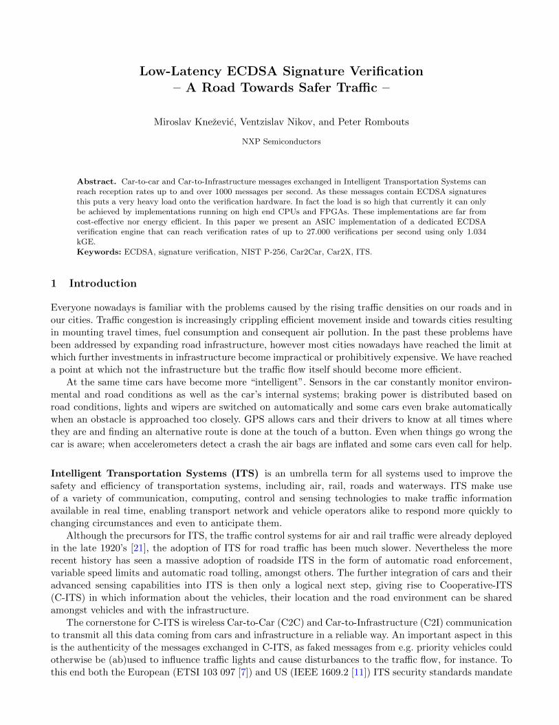
Performance Requirements. Figure 1 represents a typical dense traffic situation where a car is sur-rounded by many other cars that are constantly moving in and out its transmission range. Now, considerthis scenario occurring on a five- or six-level urban stack interchange with traffic moving on at least threelanes in each direction. It is clear to see that this easily brings us to a situation where the car is surroundedby several hundred vehicles, resulting in a large flood of Cooperative Awareness Messages (CAM) [6] to beverified every second. Assuming the channel bandwidth limitation (6 Mb/s, 256 byte messages and channelutilization of 33 %), the number of messages is limited to around 1, 000 per second. This throughput canonly be offered in a cost effective way by a highly efficient ECDSA signature verification engine such asthe one developed in this work.
However the latency is more important than throughput in the considered use case where the time toreact on a message is very important. Examples are high-priority messages police, ambulance, etc. In fact,it is really crucial that these messages get processed very fast. Therefore we would like to stress that inthis paper we focus on optimizing latency and not throughput, and they differ for example multiple-coresolutions are not suitable. Moreover our goal is to achieve this very low latency in reasonable area.
Fig. 1: Communication radius in a dense traffic (dimensions are not scaled proportionally).
Our Contribution. We introduce a high-speed ECDSA signature verification core over the NIST P-256 curve. The systematic approach and significant optimization efforts on every single level result in anarchitecture that substantially outperforms all the reported results available in literature. We prototypea core that satisfies the throughput requirement of 1, 000 verifications per second with minimal area andadditionally perform a thorough exploration of the complete design space, which yields several more designsachieving outstanding performance.
Our goal was to design an ECDSA Signature Verification engine with very low latency, in that respectwe have achieved the best results ever published, using an industry compliant technology (worst caseCMOS65). We did consider some of the newer implementation techniques but also missed many. Ourinvestigations however show that the basic “well-known” approaches are sufficient and maybe the best forASIC (HW likes simplicity). Our approach is similar to that of Guneysu and Paar [9] (CHES08) but we
focused much more on optimizing the heaviest operation, finite field multiplication and we introduced anovel approach of sau.
Organization of the Paper. We start by addressing the related work in Section 2 and outlining somepreliminaries in Section 3. The whole design process and design space exploration is discussed in Section 4.The implementation details and results are given in Section 5 and we finally conclude in Section 6.
2 Related Work
Only very few low-latency implementations of full ECDSA signature verification have been reported inliterature. Many more address the performance issues of the most common operation in ECC; the pointmultiplication. In order to have a meaningful overview and for easier comparison with our work, we outlineonly those studies that discuss performance of either point multiplication or full ECDSA signature veri-fication/generation for elliptic curves defined over a 256-bit prime field. In what comes next, we assumethat the elliptic curve arithmetic is always done in that finite field.
A very extensive study, covering many aspects of efficient software implementation of the NIST ellipticcurves over prime fields is provided by Brown et al. [2]. By implementing the finite field arithmetic inassembly language, the authors achieved very competitive results, for that time, on a Pentium II 400 MHzworkstation. A multiple point multiplication on the NIST P-256 curve took their implementation 6.4 ms.
McIvor et al. [13] presented an FPGA architecture for performing the arithmetic functions needed inelliptic curve cryptographic primitives over GF(p). Using the embedded 18×18-bit multipliers and fastcarry look-ahead logic available on the Xilinx Virtex2 Pro family of FPGA (XC2VP125-7) they were ableto tailor the architecture to perform a single point multiplication in 3.84 ms. Their implementation runsat 39.5 MHz and uses 15, 755 slices and 256 multipliers in total.
In her dissertation, Mentens [14] reports an extension of the ECC coprocessor which was previouslydescribed by Sakiyama et al. [18]. Running at a frequency of 67 MHz and using 3, 529 slices and 36embedded multipliers of the XC2VP30 development board, their implementation achieves a latency of2.27 ms for a single point multiplication. The design builds upon a pipelined architecture for the classicalmulti-precision algorithm making use of long word additions and carry-lookahead addition, as well as onthe use of non-adjacent form (NAF) recoding.
Guneysu and Paar [9] describe an ultra fast ECC implementation over two NIST primes on commercialFPGAs. Their design benefits from intensive use of the DSP blocks available in modern FPGAs and whichare especially well suited for implementation of the field operations. The paper reports a latency of 749 µsfor a multiple point multiplication over the NIST P-256 curve. Furthermore, the authors claim even fastermultiplication is possible when a windowing method is used. Their estimate of 495 µs comes at the priceof an additional 1, 715 logic slices (LS) and 32 digital signal processing (DSP) units being used on theXC4VFX12-12 Xilinx FPGA board.
Schinianakis et al. [19] take a different approach and explore the use of residue number systems (RNS)for building efficient finite field arithmetic operations. Occupying 36, 000 lookup tables (LUT) on theXCV1000E-8 Xilinx FPGA board and running at the frequency of 39.7 MHz, their implementation requires3.95 ms for a single point multiplication.
The work of Guillermin [8] is the fastest among the public hardware designs to compute scalar mul-tiplication for elliptic curves defined over a general prime ground field. The design is also based on RNS,guaranteeing carry-free arithmetic and easy parallelism. Consuming 9, 117 adaptive logic modules (ALM)on the EP2S30F484C3 Altera FPGA device and running at the frequency of 157 MHz, their implementationtakes 680 µs for a single point multiplication.
Very detailed reports on software performance of many different cryptographic algorithms can be foundat eBACS – the ECRYPT benchmarking platform of cryptographic systems [4]. Currently, the fastestimplementation of a complete ECDSA signature generation over the NIST P-256 prime achieves a latency
of only 427 µs. It comes as a surprise that this implementation, running at a frequency of 3.5 GHz onfour 64-bit cores of Intel Xeon E3 processor, is able to achieve a result that is better than any previouslyreported implementation in hardware.
3 Preliminaries
ECDSA Signature Verification. Algorithm 1 outlines basic steps of the ECDSA signature verification.The finite field is defined over the prime p and the order of the elliptic curve is denoted with n. WithP (xP , yP ) we define the base point and its coordinates and with ∞ we define the point at infinity. Themost computationally expensive operation of the algorithm is the computation of X = u1P + u2Q, veryoften referred to as a multiple point multiplication.
Algorithm 1 ECDSA Signature Verification.
Input: Curve Parameters D = (p, n, P (xP , yP )), Public Key Q(xQ, yQ),Message Hash e, Signature (r, s).
Output: accept or reject the signature.
1: if r, s /∈ [1, n− 1] then reject.2: w = s−1 mod n.3: u1 = ew mod n and u2 = rw mod n.4: X = u1P + u2Q.5: if X(x, y) =∞ then reject.6: if x mod n = r then accept else reject.
Shift-and-Add Finite Field Multiplication. A classical shift-and-add multiplication in finite field isoutlined in Alg. 2. Step 4 of the algorithm involves an integer division and is the most computationallydemanding part of it. In case M is of a special form this step can be performed rather efficiently. Next, wedemonstrate this by using an example of the NIST recommended prime. Inputs are the two l-bit integersA and B, and their product C = AB mod M is the output.
Algorithm 2 Shift-and-Add Finite Field Multiplication.
Input: A = (Alw−1 . . . A0)r, B = (Blw−1 . . . B0)r, M = (Mlw−1 . . .M0)rwhere 0 ≤ A,B < M , 2l−1 ≤M < 2l, r = 2w and lw =
⌈l/w
⌉.
Output: C = AB mod M .1: C = 02: for i = lw − 1 downto 0 do3: C = Cr +ABi
4: qC = bC/Mc5: C = C − qCM6: end for7: Return C.
NIST Modular Reduction with P-256. Due to a computationally complex operation of integer di-vision, modular reduction is considered to be an expensive task in hardware. Advanced algorithms such
as the ones of Montgomery [15] and Barrett [1] are typically used for improving the efficiency of manyconsecutive reductions with any general modulus. However, when the modulus is of a special form, themodular reduction becomes rather simplified. NIST has therefore selected a set of special primes that per-mit a very fast reduction [17]. The prime we are interested in is a 256-bit prime denoted as P-256 and equalto 2256 − 2224 + 2192 + 296 − 1. Algorithm 3 outlines the reduction procedure with this special modulus.
Algorithm 3 Modular reduction with P-256 = 2256−2224 +2192 +296−1.
Input: Integer A = (A15, . . . , A2, A1, A0) where 0 ≤ Ai < 232.Output: B = A mod P-256.
C1 = (A7, A6, A5, A4, A3, A2, A1, A0), C2 = (A15, A14, A13, A12, A11, 0, 0, 0),C3 = (0, A15, A14, A13, A12, 0, 0, 0), C4 = (A15, A14, 0, 0, 0, A10, A9, A8),C5 = (A8, A13, A15, A14, A13, A11, A10, A9), C6 = (A10, A8, 0, 0, 0, A13, A12, A11),C7 = (A11, A9, 0, 0, A15, A14, A13, A12), C8 = (A12, 0, A10, A9, A8, A15, A14, A13),C9 = (A13, 0, A11, A10, A9, 0, A15, A14).
B = C1 + 2C2 + 2C3 + C4 + C5–C6–C7–C8–C9 mod P-256.
Karatsuba Multiplication. One of the very famous multiplication algorithms that efficiently improvesthe speed of classical multiplication was discovered by Karatsuba [12] and published back in 1962. Let xand y be the two l-bit numbers and let k = dl/2e. One-level deep Karatsuba algorithm is given as follows:
xy = (xH2k + xL)(yH2k + yL)
= xHyH22k +((xH + xL)(yH + yL)− xHyH − xLyL
)2k + xLyL .
The two-level deep Karatsuba is obtained when the algorithm is applied recursively to the intermediateproducts of one-level deep Karatsuba (xHyH , (xH + xL)(yH + yL), and xLyL). If the algorithm is appliedrecursively too many times, the increasing number of additions becomes the main bottleneck of the im-plementation. Additionally, the control logic of the Karatsuba multiplier becomes more complex and, inpractice, the benefit ceases compared to the classical multiplication.
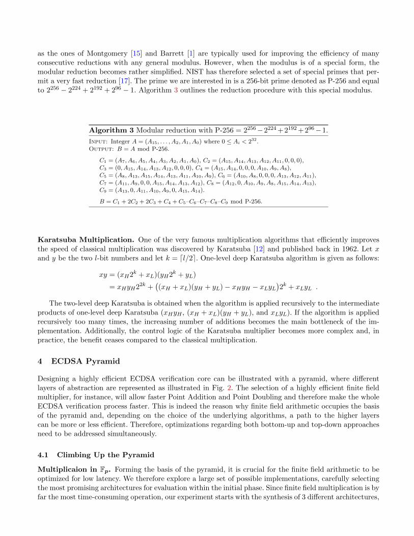
4 ECDSA Pyramid
Designing a highly efficient ECDSA verification core can be illustrated with a pyramid, where differentlayers of abstraction are represented as illustrated in Fig. 2. The selection of a highly efficient finite fieldmultiplier, for instance, will allow faster Point Addition and Point Doubling and therefore make the wholeECDSA verification process faster. This is indeed the reason why finite field arithmetic occupies the basisof the pyramid and, depending on the choice of the underlying algorithms, a path to the higher layerscan be more or less efficient. Therefore, optimizations regarding both bottom-up and top-down approachesneed to be addressed simultaneously.
4.1 Climbing Up the Pyramid
Multiplicaion in Fp. Forming the basis of the pyramid, it is crucial for the finite field arithmetic to beoptimized for low latency. We therefore explore a large set of possible implementations, carefully selectingthe most promising architectures for evaluation within the initial phase. Since finite field multiplication is byfar the most time-consuming operation, our experiment starts with the synthesis of 3 different architectures,
FINITE FIELDARITHMETIC
POINT ADDPOINT DBL
JSF, NAF,
Windowing,
Projective
Coordinates
ECDSA ACCEPT
a + b mod m
a × b mod m
a-1 mod m
REJECT
Fig. 2: ECDSA pyramid.
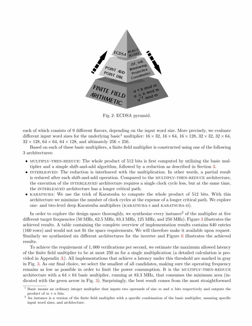
each of which consists of 9 different flavors, depending on the input word size. More precisely, we evaluatedifferent input word sizes for the underlying basic1 multiplier: 16× 32, 16× 64, 16× 128, 32× 32, 32× 64,32× 128, 64× 64, 64× 128, and ultimately 256× 256.
Based on each of these basic multipliers, a finite field multiplier is constructed using one of the following3 architectures:
• multiply-then-reduce: The whole product of 512 bits is first computed by utilizing the basic mul-tiplier and a simple shift-and-add algorithm, followed by a reduction as described in Section 3.• interleaved: The reduction is interleaved with the multiplication. In other words, a partial result
is reduced after each shift-and-add operation. Compared to the multiply-then-reduce architecture,the execution of the interleaved architecture requires a single clock cycle less, but at the same time,the interleaved architecture has a longer critical path.• karatsuba: We use the trick of Karatsuba to compute the whole product of 512 bits. With this
architecture we minimize the number of clock cycles at the expense of a longer critical path. We exploreone- and two-level deep Karatsuba multipliers (karatsuba-i and karatsuba-ii).
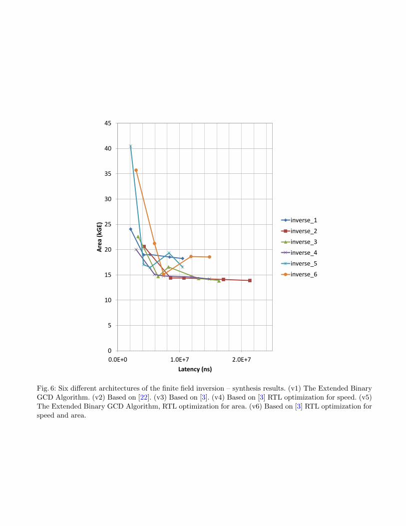
In order to explore the design space thoroughly, we synthesize every instance2 of the multiplier at fivedifferent target frequencies (50 MHz, 62.5 MHz, 83.3 MHz, 125 MHz, and 250 MHz). Figure 3 illustrates theachieved results. A table containing the complete overview of implementation results contains 640 entries(160 rows) and would not not fit the space requirements. We will therefore make it available upon request.Similarly we synthesized six different architectures for the inverter and Figure 6 illustrates the achievedresults.
To achieve the requirement of 1, 000 verifications per second, we estimate the maximum allowed latencyof the finite field multiplier to be at most 250 ns for a single multiplication (a detailed calculation is pro-vided in Appendix A). All implementations that achieve a latency under this threshold are marked in grayin Fig. 3. As our final choice, we select the smallest of all candidates, making sure the operating frequencyremains as low as possible in order to limit the power consumption. It is the multiply-then-reducearchitecture with a 64 × 64 basic multiplier, running at 83.3 MHz, that consumes the minimum area (in-dicated with the green arrow in Fig. 3). Surprisingly, the best result comes from the most straightforward
1 Basic means an ordinary integer multiplier that inputs two operands of size m and n bits respectively and outputs theproduct of m+ n bits.
2 An instance is a version of the finite field multiplier with a specific combination of the basic multiplier, meaning specificinput word sizes, and architecture.
50100
150200
25016x32
16x64
32x32
32x64
64x640
100
200
300
400
500
60 80 10012014016018020022016x32
16x6416x128
32x3232x6432x128
64x6464x128
0
500
1000
1500
40 6080
100120
140160
16x3216x6416x128
32x3232x6432x128
64x6464x128
0
500
1000
1500
2000
2500
4060
80100
120140
16016x32
16x6416x128
32x3232x6432x128
64x6464x128
0
500
1000
1500
2000
2500
Late
ncy
(n
s)
Late
ncy
(n
s)La
ten
cy (
ns)
Area (kGE)Area (kGE)
Late
ncy
(n
s)
Area (kGE)Area (kGE)
MTR-64x6444.7kGE @ 83.3MHz
(a) (b)
(d)(c)
Fig. 3: Four different architectures of the finite field multiplier – synthesis results. (a) multiply-then-reduce. (b) interleaved. (c) karatsuba-i one-level deep. (d) karatsuba-ii two-level deep.
architecture where the multiplication and reduction parts are simply performed consecutively (multiply-then-reduce). One would expect that more advanced techniques, such as interleaved or Karatsuba mul-tiplication, would result in better performance. There is however an easy explanation.
We first observe all of the synthesized designs and compare them to the multiply-then-reduce archi-tecture. Out of 40 synthesized instances of interleaved, 33 perform better than corresponding multiply-then-reduce instances (for the same latency, area is smaller). The reason for this is simple. When botharchitectures are synthesized for frequencies that are considerably lower than their inverted shortest criticalpath, the interleaved architecture provides better figures due to the smaller reduction part. Recall thatthe reduction part of multiply-then-reduce reduces 512-bit integers to 256-bit integers in a single clockcycle, while the reduction of interleaved reduces an m + n + 256-bit integer to a 256-bit one (m andn are the operand sizes of the basic multiplier as indicated previously). When the operating frequency isincreased, however, the interleaved architecture reaches its shortest critical path faster than multiply-then-reduce. This is obvious since, due to the merged multiplication and reduction part, the critical pathof interleaved is longer than the critical path of multiply-then-reduce. Synthesizing for a frequency
of 83.3 MHz (i.e. 12 ns) obviously causes interleaved to increase its size considerably more than thearchitecture of multiply-then-reduce.
Although achieving lower latency, the architectures based on Karatsuba algorithm have a larger circuitarea, mainly due to the complex structure of datapath and control logic. Note that the same basic multipliersare used for all the explored architectures and, thus, the overhead comes from the circuitry for correctscheduling, the reduction part, and the temporary storage.
4.2 Skiing Down the Pyramid
Point Addition & Point Doubling. We start the top-down approach by identifying an appropriatecoordinate system. Our goal is to avoid area-consuming storage, while still providing maximal speed upfor the signature verification process. Examination of a set of possible projective coordinates lead us tothe selection of Jacobian coordinates for point doubling (dbl) and mixed coordinates (affine-Jacobian) forpoint addition (add). In order to facilitate implementation we introduce a simple arithmetic unit (sau)that prepares operands before they enter the finite field multiplier.The sau supports very simple modularoperations such as addition, subtraction, multiplication with 2 (left shift) and division by 2 (right shift). Itis a purely combinational block without any storage. This way we are able to reduce the number of cyclesin both add and dbl algorithms which is crucial for lowering the latency. Moreover, we save two temporaryregisters, each of 256 bits, compared to the originally proposed algorithms [10]. This way we gain back thearea initially invested in the sau. After a slight modification of both add and dbl algorithms, we proposethe following two formulas (Table 1).
Table 1: Point Addition & Point Doubling.
ADD DBL
T1 = Z12 T2 = X1− Z12
T2 = T1Z1 T2 = 3T2(2X1− T2)T2 = T2Y 2− Y 1 X3 = T22
T1 = T1X2−X1 Z3 = 2Y 1Z1Z3 = Z1T1 Y 3 = (2Y 1)2
Y 3 = T12 X3 = X3− 2Y 3X1X3 = T22 T1 = (Y 3X1∗ −X3)T2T1 = Y 3T1 Y 3 = T1− (Y 32)/2
X3 = X3− T1− 2Y 3X1Y 3 = (Y 3X1∗ −X3)T2
Y 3 = Y 3− T1Y 1
Y 3X1∗ is fed directly as a product from the previous step.
Each step of the two algorithms consists of at most one single finite field multiplication and a fewbasic operations. Steps denoted with asterisk (*) may seem to consist of two multiplications, however whatoccurs in fact is that the product from the previous step (Y 3X1) is directly fed back into the finite fieldmultiplier after subtracting X3 from it. With this approach save one temporary register.
Based on the selection of these algorithms, we further explore the possibility of using one or more ofthe multiplier cores of the previous section. Due to the dependencies in both the add and dbl algorithms,it is apparent that the multi-core approach brings no significant advantages. In other words, for the priceof an additional multiplier core, the improvement in speed is only 27.3 % for add and 25 % for dbl, whiledepending on the multiplier architecture, its circuitry consumes at least one third of the overall core size.Table 2 shows the analysis.
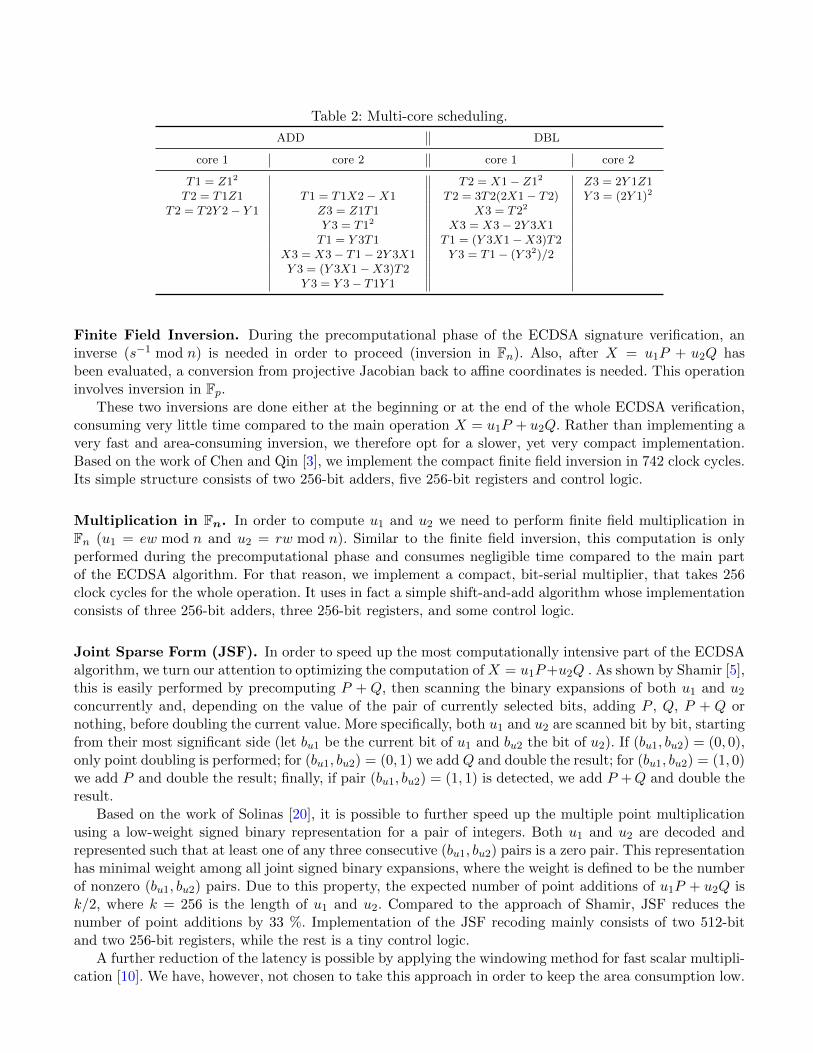
Table 2: Multi-core scheduling.
ADD DBL
core 1 core 2 core 1 core 2
T1 = Z12 T2 = X1− Z12 Z3 = 2Y 1Z1T2 = T1Z1 T1 = T1X2−X1 T2 = 3T2(2X1− T2) Y 3 = (2Y 1)2
T2 = T2Y 2− Y 1 Z3 = Z1T1 X3 = T22
Y 3 = T12 X3 = X3− 2Y 3X1T1 = Y 3T1 T1 = (Y 3X1−X3)T2
X3 = X3− T1− 2Y 3X1 Y 3 = T1− (Y 32)/2Y 3 = (Y 3X1−X3)T2Y 3 = Y 3− T1Y 1
Finite Field Inversion. During the precomputational phase of the ECDSA signature verification, aninverse (s−1 mod n) is needed in order to proceed (inversion in Fn). Also, after X = u1P + u2Q hasbeen evaluated, a conversion from projective Jacobian back to affine coordinates is needed. This operationinvolves inversion in Fp.
These two inversions are done either at the beginning or at the end of the whole ECDSA verification,consuming very little time compared to the main operation X = u1P + u2Q. Rather than implementing avery fast and area-consuming inversion, we therefore opt for a slower, yet very compact implementation.Based on the work of Chen and Qin [3], we implement the compact finite field inversion in 742 clock cycles.Its simple structure consists of two 256-bit adders, five 256-bit registers and control logic.
Multiplication in Fn. In order to compute u1 and u2 we need to perform finite field multiplication inFn (u1 = ew mod n and u2 = rw mod n). Similar to the finite field inversion, this computation is onlyperformed during the precomputational phase and consumes negligible time compared to the main partof the ECDSA algorithm. For that reason, we implement a compact, bit-serial multiplier, that takes 256clock cycles for the whole operation. It uses in fact a simple shift-and-add algorithm whose implementationconsists of three 256-bit adders, three 256-bit registers, and some control logic.
Joint Sparse Form (JSF). In order to speed up the most computationally intensive part of the ECDSAalgorithm, we turn our attention to optimizing the computation of X = u1P+u2Q . As shown by Shamir [5],this is easily performed by precomputing P + Q, then scanning the binary expansions of both u1 and u2concurrently and, depending on the value of the pair of currently selected bits, adding P , Q, P + Q ornothing, before doubling the current value. More specifically, both u1 and u2 are scanned bit by bit, startingfrom their most significant side (let bu1 be the current bit of u1 and bu2 the bit of u2). If (bu1, bu2) = (0, 0),only point doubling is performed; for (bu1, bu2) = (0, 1) we add Q and double the result; for (bu1, bu2) = (1, 0)we add P and double the result; finally, if pair (bu1, bu2) = (1, 1) is detected, we add P +Q and double theresult.
Based on the work of Solinas [20], it is possible to further speed up the multiple point multiplicationusing a low-weight signed binary representation for a pair of integers. Both u1 and u2 are decoded andrepresented such that at least one of any three consecutive (bu1, bu2) pairs is a zero pair. This representationhas minimal weight among all joint signed binary expansions, where the weight is defined to be the numberof nonzero (bu1, bu2) pairs. Due to this property, the expected number of point additions of u1P + u2Q isk/2, where k = 256 is the length of u1 and u2. Compared to the approach of Shamir, JSF reduces thenumber of point additions by 33 %. Implementation of the JSF recoding mainly consists of two 512-bitand two 256-bit registers, while the rest is a tiny control logic.
A further reduction of the latency is possible by applying the windowing method for fast scalar multipli-cation [10]. We have, however, not chosen to take this approach in order to keep the area consumption low.
a × b mod p+
SAU
MEMORY
FSM
clk
rst_an
verif_start
pub_key_valid
msg_hash_valid
msg_sign_valid
pub_key msg_hash msg_sign
a × b mod n
a-1 mod m
JSF
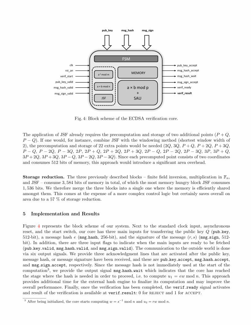
Fig. 4: Block scheme of the ECDSA verification core.
The application of JSF already requires the precomputation and storage of two additional points (P +Q,P − Q). If one would, for instance, combine JSF with the windowing method (shortest window width of2), the precomputation and storage of 22 extra points would be needed (2Q, 3Q, P +Q, P + 2Q, P + 3Q,P − Q, P − 2Q, P − 3Q, 2P , 2P + Q, 2P + 2Q, 2P + 3Q, 2P − Q, 2P − 2Q, 2P − 3Q, 3P , 3P + Q,3P + 2Q, 3P + 3Q, 3P −Q, 3P − 2Q, 3P − 3Q). Since each precomputed point consists of two coordinatesand consumes 512 bits of memory, this approach would introduce a significant area overhead.
Storage reduction. The three previously described blocks – finite field inversion, multiplication in Fn,and JSF – consume 3, 584 bits of memory in total, of which the most memory hungry block JSF consumes1, 536 bits. We therefore merge the three blocks into a single one where the memory is efficiently sharedamongst them. This comes at the expense of a more complex control logic but certainly saves overall onarea due to a 57 % of storage reduction.
5 Implementation and Results
Figure 4 represents the block scheme of our system. Next to the standard clock input, asynchronousreset, and the start switch, our core has three main inputs for transferring the public key Q (pub key,512-bit), a message hash e (msg hash, 256-bit), and the signature of the message (r, s) (msg sign, 512-bit). In addition, there are three input flags to indicate when the main inputs are ready to be fetched(pub key valid, msg hash valid, and msg sign valid). The communication to the outside world is donevia six output signals. We provide three acknowledgment lines that are activated after the public key,message hash, or message signature have been received, and these are pub key accept, msg hash accept,and msg sign accept, respectively. Since the message hash is not immediately used at the start of thecomputation3, we provide the output signal msg hash wait which indicates that the core has reachedthe stage where the hash is needed in order to proceed, i.e. to compute u1 = ew mod n. This approachprovides additional time for the external hash engine to finalize its computation and may improve theoverall performance. Finally, once the verification has been completed, the verif ready signal activatesand result of the verification is available at verif result: 0 for reject and 1 for accept.
3 After being initialized, the core starts computing w = s−1 mod n and u2 = rw mod n.
The core consists of several independent modules, which are controlled by a finite state machine (fsm).The largest of all, a finite field multiplier together with the sau, represents the heart of the core andconsumes most of the total computation time. In order to share the memory resources, finite field inversion(both in Fp and Fn), multiplication in Fn, and JSF blocks are merged into one and denoted with the dashedrectangle in Fig. 4. Memory, except of a few very dedicated registers inside the big multiplier, is sharedbetween all other resources. Different sau architectures are given in Fig. 5
Next, we provide the implementation results of the ECDSA core. The RTL code has been written inVerilog and tested against more than 100,000 test vectors, covering all classes of corner cases4. The synthesishas been carried out in Cadence RTL Compiler version 11.10-p005 and we used two different libraries forthat purpose. The library which is used for the final prototype is 65 nm TSMC CMOS process with theworst case PVT conditions (125◦ C temperature and 0.8 V supply). In order to allow future comparisonsto our core, we additionally provide the synthesis results using an open core NANGATE library, releasePDKv1.3 2010 12 [16]. This is a 45 nm CMOS process with typical case PVT conditions (25◦ C temperatureand 1.1 V supply).
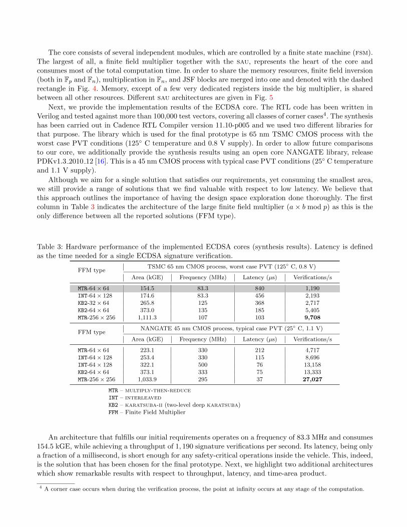
Although we aim for a single solution that satisfies our requirements, yet consuming the smallest area,we still provide a range of solutions that we find valuable with respect to low latency. We believe thatthis approach outlines the importance of having the design space exploration done thoroughly. The firstcolumn in Table 3 indicates the architecture of the large finite field multiplier (a× b mod p) as this is theonly difference between all the reported solutions (FFM type).
Table 3: Hardware performance of the implemented ECDSA cores (synthesis results). Latency is definedas the time needed for a single ECDSA signature verification.
FFM typeTSMC 65 nm CMOS process, worst case PVT (125◦ C, 0.8 V)
Area (kGE) Frequency (MHz) Latency (µs) Verifications/s
MTR-64× 64 154.5 83.3 840 1,190INT-64× 128 174.6 83.3 456 2,193KB2-32× 64 265.8 125 368 2,717KB2-64× 64 373.0 135 185 5,405MTR-256× 256 1,111.3 107 103 9,708
FFM typeNANGATE 45 nm CMOS process, typical case PVT (25◦ C, 1.1 V)
Area (kGE) Frequency (MHz) Latency (µs) Verifications/s
MTR-64× 64 223.1 330 212 4,717INT-64× 128 253.4 330 115 8,696INT-64× 128 322.1 500 76 13,158KB2-64× 64 373.1 333 75 13,333MTR-256× 256 1,033.9 295 37 27,027
MTR – multiply-then-reduceINT – interleavedKB2 – karatsuba-ii (two-level deep karatsuba)FFM – Finite Field Multiplier
An architecture that fulfills our initial requirements operates on a frequency of 83.3 MHz and consumes154.5 kGE, while achieving a throughput of 1, 190 signature verifications per second. Its latency, being onlya fraction of a millisecond, is short enough for any safety-critical operations inside the vehicle. This, indeed,is the solution that has been chosen for the final prototype. Next, we highlight two additional architectureswhich show remarkable results with respect to throughput, latency, and time-area product.
4 A corner case occurs when during the verification process, the point at infinity occurs at any stage of the computation.
Although it comes at the price of 1.1 million gate equivalences, our core with the MTR-256×256 multiplierachieves more than 27, 000 signature verifications per second. To the best of the authors knowledge, thisis the fastest reported implementation of P-256 ECDSA signature verification on a single core. In [9], theauthors report a performance of 16, 352 multiple points multiplications per second over the P-256 ellipticcurve on a single chip5 (Virtex-4 FPGA device). Their implementation, however, consists of 16 independentcores running in parallel, which translates the overall throughput to 1, 022 multiple points multiplicationsper second per single core.
When observing the latency, our fastest architecture is able to verify a single signature in only 37 µswhile previously the fastest implementation, which is in fact a software implementation of an ECDSAsignature generation, comes from [4] and reports a latency of 427 µs. The previously fastest hardwareimplementation comes from [8] with 680 µs for a single point multiplication. Another notable result isreported in [9], where the multiple point multiplication on a single core takes 749 µs. The authors furtherestimate that in case the windowing method is used, the latency can be improved to 495 µs. We have tonote here that a fair comparison between these designs is very difficult since the technology used is differentin these three cases (ASIC versus FPGA versus software), although in a system design all three optionscould be weighed against each other.
Finally, by observing the efficiency of proposed architectures, we highlight the INT-64× 128 core whichdelivers the highest throughput per area. Its time-area product equals only 24.5 sGE.
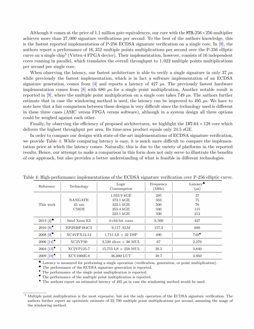
In order to compare our designs with state-of-the-art implementations of ECDSA signature verification,we provide Table 4. While comparing latency is easy, it is much more difficult to compare the implemen-tation price at which the latency comes. Naturally, this is due to the variety of platforms in the reportedresults. Hence, our attempt to make a comparison in this form does not only serve to illustrate the benefitsof our approach, but also provides a better understanding of what is feasible in different technologies.
Table 4: High-performance implementations of the ECDSA signature verification over P-256 elliptic curve.
Reference TechnologyLogic Frequency Latency♣
Consumption (MHz) (µs)
This work
1,033.9 kGE 295 37NANGATE 373.1 kGE 333 75
45 nm 322.1 kGE 500 76CMOS 253.4 kGE 330 115
223.1 kGE 330 212
2013 [4]♠ Intel Xeon E3 4×64-bit cores 3, 500 427
2010 [8]♦ EP2S30F484C3 9,117 ALM 157.2 680
2008 [9]♥ XC4VFX12-12 1,715 LS + 32 DSP 490 749F
2006 [14]♦ XC2VP30 3,529 slices + 36 MUL 67 2,270
2004 [13]♦ XC2VP125-7 15,755 LS + 256 MUL 39.5 3,840
2009 [19]♦ XCV1000E-8 36,000 LUT 39.7 3,950
♣ Latency is measured for performing a single operation (verification, generation, or point multiplication).♠ The performance of the ECDSA signature generation is reported.♦ The performance of the single point multiplication is reported.♥ The performance of the multiple point multiplication is reported.F The authors report an estimated latency of 495 µs in case the windowing method would be used.
5 Multiple point multiplication is the most expensive, but not the only operation of the ECDSA signature verification. Theauthors further report an optimistic estimate of 22, 700 multiple point multiplications per second, assuming the usage ofthe windowing method.
6 Conclusion
We have presented the fastest core for performing a digital signature verification based on elliptic curvesover the NIST P-256 prime. The results achieved in this work, including amongst others a latency of37 µs for a single signature verification and an efficiency of 24.5 sGE, significantly outperform any previousimplementation known by the authors.
We have further shown that it is possible to meet the requirements for Car2X communication securityin intelligent transportation systems – signature verification in less than a millisecond – with a core of only155 kGE, providing a much more cost effective solution for mass production compared to any software orFPGA based solution.
References
1. P. Barrett. Implementing the Rivest Shamir and Adleman Public Key Encryption Algorithm on a Standard Digital SignalProcessor. In Advances in Cryptology — CRYPTO ’86, volume 263 of Lecture Notes in Computer Science, pages 311–323.Springer, 1987.
2. M. Brown, D. Hankerson, J. Lopez, and A. Menezes. Software Implementation of the NIST Elliptic Curves Over PrimeFields. Lecture Notes in Computer Science, 2020, 2001.
3. C. Chen and Z. Qin. Fast Algorithm and Hardware Architecture for Modular Inversion in GF(p). In Intelligent Networksand Intelligent Systems, 2009. ICINIS ’09. Second International Conference on, pages 43–45, 2009.
4. D. J. Bernstein and T. Lange (editors). eBACS: ECRYPT Benchmarking of Cryptographic Systems. Available athttp://bench.cr.yp.to/ebats.html, accessed 14 Janruary 2014.
5. T. ElGamal. A Public Key Cryptosystem and a Signature Scheme Based on Discrete Logarithms. In Advances inCryptology — CRYPTO ’85, volume 218 of Lecture Notes in Computer Science, pages 10–18. Springer, 1986.
6. ETSI TS 102 637-2 V1.2.1 (2011-03). Technical Specification; Intelligent Transport Systems (ITS); Vehicular Communi-cations; Basic Set of Applications; Part 2: Specification of Co-operative Awareness Basic Service.
7. ETSI TS 103 097 V0.0.13 (2013-02). Technical Specification; Intelligent Transport Systems (ITS); Security; SecurityServices and Architecture.
8. N. Guillermin. A High Speed Coprocessor for Elliptic Curve Scalar Multiplications over Fp. In Cryptographic Hardwareand Embedded Systems — CHES 2010, volume 6225 of Lecture Notes in Computer Science, pages 48–64. Springer, 2010.
9. T. Guneysu and C. Paar. Ultra High Performance ECC over NIST Primes on Commercial FPGAs. In CryptographicHardware and Embedded Systems — CHES 2008, volume 5154 of Lecture Notes in Computer Science, pages 62–78.Springer, 2008.
10. D. Hankerson, A. Menezes, and S. Vanstone. Guide to Elliptic Curve Cryptography. Springer-Verlag, 2004.11. IEEE Std 1609.2-2006. IEEE Trial-Use Standard for Wireless Access in Vehicular Environments - Security Services for
Applications and Management Messages.12. A. Karatsuba and Y. Ofman. Multiplication of Many-Digital Numbers by Automatic Computers. Soviet Physics - Doklady,
7:595–596, 1962. Translation from Doklady Akademii Nauk SSSR, 145:2, 293–294, 1962.13. C. McIvor, M. McLoone, and J. McCanny. An FPGA Elliptic Curve Cryptographic Accelerator Over GF(p). In Irish
Signals and Systems Conference (ISSC), pages 589–594, 2004.14. N. Mentens. Secure and Effcient Coprocessor Design for Cryptographic Applications on FPGAs. PhD thesis, Katholieke
Universiteit Leuven, 2007.15. P. Montgomery. Modular Multiplication without Trial Division. Mathematics of Computation, 44(170):519–521, 1985.16. NANGATE. The NanGate 45nm Open Cell Library. Available at http://www.nangate.com.17. National Institute of Standards and Technology (NIST). FIPS 186-3: Digital Signature Standard, 2009. Available at
http://csrc.nist.gov/.18. K. Sakiyama, E. De Mulder, B. Preneel, and I. Verbauwhede. A Parallel Processing Hardware Architecture for Elliptic
Curve Cryptosystems. IEEE ICASSP, pages 904–907, 2006.19. D. Schinianakis, A. Fournaris, H. Michail, A. Kakarountas, and T. Stouraitis. An RNS Implementation of an Elliptic
Curve Point Multiplier. IEEE Transactions on Circuits and Systems I, 56(6):1202–1213, 2009.20. J. A. Solinas. Low-Weight Binary Representations for Pairs of Integers. Technical report, National Security Agency, USA,
2001.21. Traffic Control. Encyclopedia Britannica. Available at http://www.britannica.com/.22. T. Zhou, X. Wu, G. Bai, and H. Chen. Fast GF(p) Modular Inversion Algorithm Suitable for VLSI Implementation.
38(14):706–707, July 2002.
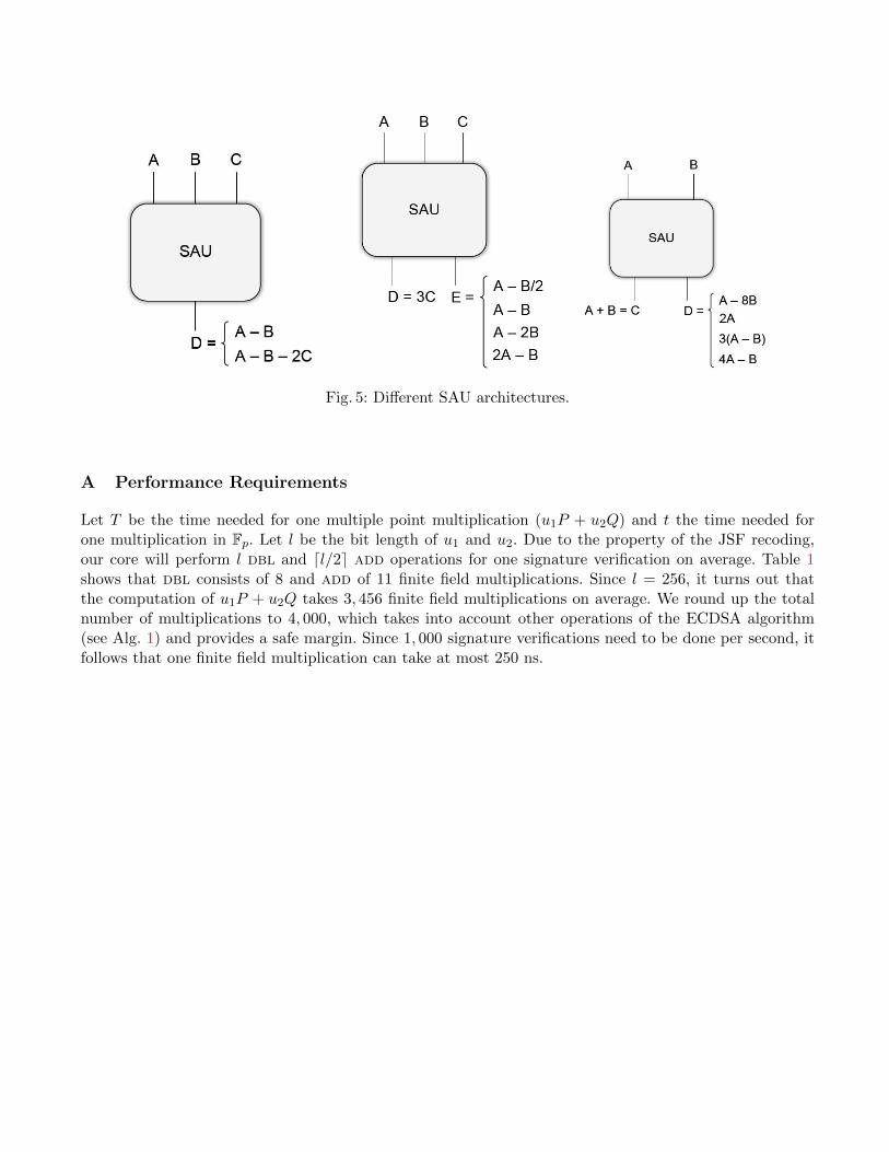
Fig. 5: Different SAU architectures.
A Performance Requirements
Let T be the time needed for one multiple point multiplication (u1P + u2Q) and t the time needed forone multiplication in Fp. Let l be the bit length of u1 and u2. Due to the property of the JSF recoding,our core will perform l dbl and dl/2e add operations for one signature verification on average. Table 1shows that dbl consists of 8 and add of 11 finite field multiplications. Since l = 256, it turns out thatthe computation of u1P + u2Q takes 3, 456 finite field multiplications on average. We round up the totalnumber of multiplications to 4, 000, which takes into account other operations of the ECDSA algorithm(see Alg. 1) and provides a safe margin. Since 1, 000 signature verifications need to be done per second, itfollows that one finite field multiplication can take at most 250 ns.
0
5
10
15
20
25
30
35
40
45
0.0E+0 1.0E+7 2.0E+7
Are
a (k
GE)
Latency (ns)
inverse_1
inverse_2
inverse_3
inverse_4
inverse_5
inverse_6
Fig. 6: Six different architectures of the finite field inversion – synthesis results. (v1) The Extended BinaryGCD Algorithm. (v2) Based on [22]. (v3) Based on [3]. (v4) Based on [3] RTL optimization for speed. (v5)The Extended Binary GCD Algorithm, RTL optimization for area. (v6) Based on [3] RTL optimization forspeed and area.