Embed Size (px)
Citation preview
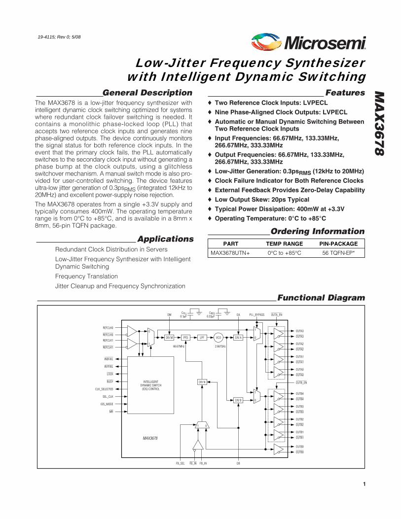
General DescriptionThe MAX3678 is a low-jitter frequency synthesizer withintelligent dynamic clock switching optimized for systemswhere redundant clock failover switching is needed. Itcontains a monolithic phase-locked loop (PLL) thataccepts two reference clock inputs and generates ninephase-aligned outputs. The device continuously monitorsthe signal status for both reference clock inputs. In theevent that the primary clock fails, the PLL automaticallyswitches to the secondary clock input without generating aphase bump at the clock outputs, using a glitchlessswitchover mechanism. A manual switch mode is also pro-vided for user-controlled switching. The device featuresultra-low jitter generation of 0.3psRMS (integrated 12kHz to20MHz) and excellent power-supply noise rejection.
The MAX3678 operates from a single +3.3V supply andtypically consumes 400mW. The operating temperaturerange is from 0°C to +85°C, and is available in a 8mm x8mm, 56-pin TQFN package.
ApplicationsRedundant Clock Distribution in Servers
Low-Jitter Frequency Synthesizer with IntelligentDynamic Switching
Frequency Translation
Jitter Cleanup and Frequency Synchronization
Features♦ Two Reference Clock Inputs: LVPECL
♦ Nine Phase-Aligned Clock Outputs: LVPECL
♦ Automatic or Manual Dynamic Switching BetweenTwo Reference Clock Inputs
♦ Input Frequencies: 66.67MHz, 133.33MHz,266.67MHz, 333.33MHz
♦ Output Frequencies: 66.67MHz, 133.33MHz,266.67MHz, 333.33MHz
♦ Low-Jitter Generation: 0.3psRMS (12kHz to 20MHz)
♦ Clock Failure Indicator for Both Reference Clocks
♦ External Feedback Provides Zero-Delay Capability
♦ Low Output Skew: 20ps Typical
♦ Typical Power Dissipation: 400mW at +3.3V
♦ Operating Temperature: 0°C to +85°C
MA
X3
67
8
Ordering Information
MAX3678
INTELLIGENTDYNAMIC SWITCH
(IDS) CONTROL
IN0FAIL
IN1FAIL
LOCK
BUSY
CLK_SELECTED
SEL_CLK
IDS_MODE
MR
REFCLK0
REFCLK0
FB_INFB_SEL FB_IN
REFCLK1
REFCLK1
0
1
1
0DIV M
DM DA
DB
PFD LPF
DIV N
DIV A
DIV B
VCO
2.667GHz66.67MHzOUTA2
OUTA2
OUTA1
OUTA1
OUTA3
OUTA3
OUTA0
OUTB_EN
OUTA0
OUTA_ENPLL_BYPASS
1
0
1 0
OUTB3
OUTB3
OUTB2
OUTB2
OUTB4
OUTB4
OUTB1
OUTB1
OUTB0
OUTB0
CPLL0.1μF
CREG0.22μF
PART TEMP RANGE PIN-PACKAGE
MAX3678UTN+ 0°C to +85°C 56 TQFN-EP*
E V A L U A T I O N K I T A V A I L A B L E
19-4115; Rev 0; 5/08
with Intelligent Dynamic Switching Low-Jitter Frequency Synthesizer
Functional Diagram
1
MA
X3
67
8
Low-Jitter Frequency Synthesizer withIntelligent Dynamic Switching
2 _______________________________________________________________________________________
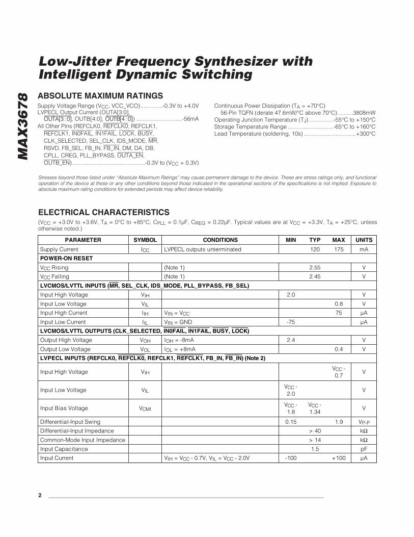
ABSOLUTE MAXIMUM RATINGS
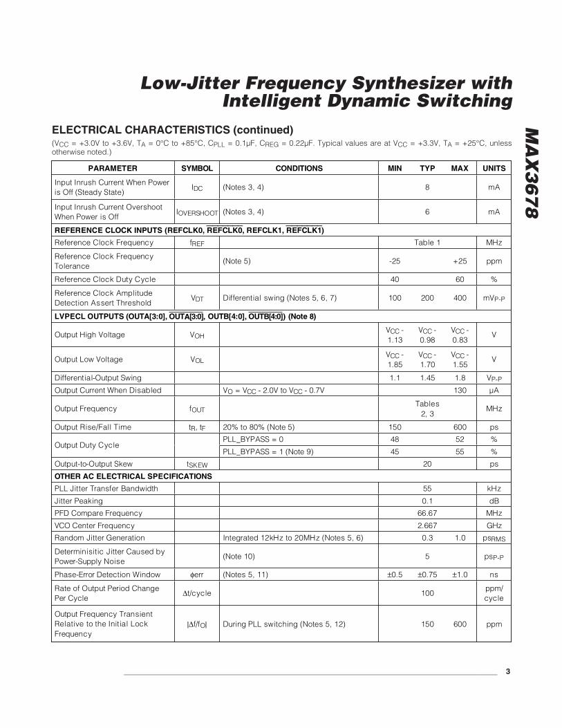
ELECTRICAL CHARACTERISTICS(VCC = +3.0V to +3.6V, TA = 0°C to +85°C, CPLL = 0.1µF, CREG = 0.22µF. Typical values are at VCC = +3.3V, TA = +25°C, unlessotherwise noted.)
Stresses beyond those listed under “Absolute Maximum Ratings” may cause permanent damage to the device. These are stress ratings only, and functionaloperation of the device at these or any other conditions beyond those indicated in the operational sections of the specifications is not implied. Exposure toabsolute maximum rating conditions for extended periods may affect device reliability.
Supply Voltage Range (VCC, VCC_VCO)..............-0.3V to +4.0VLVPECL Output Current (OUTA[3:0],
, OUTB[4:0], ) .............................-56mAAll Other Pins (REFCLK0, REFCLK0, REFCLK1,
REFCLK1, IN0FAIL, IN1FAIL, LOCK, BUSY,CLK_SELECTED, SEL_CLK, IDS_MODE, MR,RSVD, FB_SEL, FB_IN, FB_IN, DM, DA, DB,CPLL, CREG, PLL_BYPASS, OUTA_EN,OUTB_EN) ..............................................-0.3V to (VCC + 0.3V)
Continuous Power Dissipation (TA = +70°C)56-Pin TQFN (derate 47.6mW/°C above 70°C)..........3808mW
Operating Junction Temperature (TJ)................-55°C to +150°CStorage Temperature Range .............................-65°C to +160°CLead Temperature (soldering, 10s) .................................+300°C
OUTB[ : ]4 0OUTA[ : ]3 0
PARAMETER SYMBOL CONDITIONS MIN TYP MAX UNITS
Supply Current ICC LVPECL outputs unterminated 120 175 mA
POWER-ON RESET
VCC Rising (Note 1) 2.55 V
VCC Falling (Note 1) 2.45 V
LVCMOS/LVTTL INPUTS (MR, SEL_CLK, IDS_MODE, PLL_BYPASS, FB_SEL)
Input High Voltage VIH 2.0 V
Input Low Voltage VIL 0.8 V
Input High Current IIH VIN = VCC 75 μA
Input Low Current IIL VIN = GND -75 μA
LVCMOS/LVTTL OUTPUTS (CLK_SELECTED, IN0FAIL, IN1FAIL, BUSY, LOCK)
Output High Voltage VOH IOH = -8mA 2.4 V
Output Low Voltage VOL IOL = +8mA 0.4 V
LVPECL INPUTS (REFCLK0, REFCLK0, REFCLK1, REFCLK1, FB_IN, FB_IN) (Note 2)
Input High Voltage VIH VCC - 0.7
V
Input Low Voltage VILVCC - 2.0
V
Input Bias Voltage VCMIVCC - 1.8
VCC - 1.34
V
Differential-Input Swing 0.15 1.9 VP-P
Differential-Input Impedance > 40 k
Common-Mode Input Impedance > 14 k
Input Capacitance 1.5 pF
Input Current VIH = VCC - 0.7V, VIL = VCC - 2.0V -100 +100 μA
MA
X3
67
8
Low-Jitter Frequency Synthesizer withIntelligent Dynamic Switching
_______________________________________________________________________________________ 3
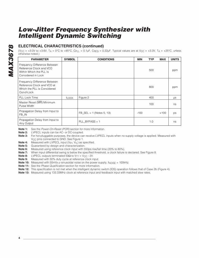
ELECTRICAL CHARACTERISTICS (continued)(VCC = +3.0V to +3.6V, TA = 0°C to +85°C, CPLL = 0.1µF, CREG = 0.22µF. Typical values are at VCC = +3.3V, TA = +25°C, unlessotherwise noted.)
PARAMETER SYMBOL CONDITIONS MIN TYP MAX UNITS
Input Inrush Current When Power is Off (Steady State)
IDC (Notes 3, 4) 8 mA
Input Inrush Current Overshoot When Power is Off
IOVERSHOOT (Notes 3, 4) 6 mA
REFERENCE CLOCK INPUTS (REFCLK0, REFCLK0, REFCLK1, REFCLK1)
Reference Clock Frequency fREF Table 1 MHz
Reference Clock Frequency Tolerance
(Note 5) -25 +25 ppm
Reference Clock Duty Cycle 40 60 %
Reference Clock Amplitude Detection Assert Threshold
VDT Differential swing (Notes 5, 6, 7) 100 200 400 mVP-P
LVPECL OUTPUTS (OUTA[3:0], OUTA[3:0], OUTB[4:0], OUTB[4:0]) (Note 8)
Output High Voltage VOHVCC - 1.13
VCC - 0.98
VCC - 0.83
V
Output Low Voltage VOLVCC - 1.85
VCC - 1.70
VCC - 1.55
V
Differential-Output Swing 1.1 1.45 1.8 VP-P
Output Current When Disabled VO = VCC - 2.0V to VCC - 0.7V 130 μA
Output Frequency fOUT Tables
2, 3 MHz
Output Rise/Fall Time tR, tF 20% to 80% (Note 5) 150 600 ps
PLL_BYPASS = 0 48 52 % Output Duty Cycle
PLL_BYPASS = 1 (Note 9) 45 55 %
Output-to-Output Skew tSKEW 20 ps
OTHER AC ELECTRICAL SPECIFICATIONS
PLL Jitter Transfer Bandwidth 55 kHz
Jitter Peaking 0.1 dB
PFD Compare Frequency 66.67 MHz
VCO Center Frequency 2.667 GHz
Random Jitter Generation Integrated 12kHz to 20MHz (Notes 5, 6) 0.3 1.0 psRMS
Determinisitic Jitter Caused by Power-Supply Noise
(Note 10) 5 psP-P
Phase-Error Detection Window err (Notes 5, 11) ±0.5 ±0.75 ±1.0 ns
Rate of Output Period Change Per Cycle
t/cycle 100 ppm/ cycle
Output Frequency Transient Relative to the Initial Lock Frequency
| f/fO| During PLL switching (Notes 5, 12) 150 600 ppm
MA
X3
67
8
Low-Jitter Frequency Synthesizer withIntelligent Dynamic Switching
4 _______________________________________________________________________________________
Note 1: See the Power-On-Reset (POR) section for more information. Note 2: LVPECL inputs can be AC- or DC-coupled.Note 3: For hot-pluggable purposes, the device can receive LVPECL inputs when no supply voltage is applied. Measured with
VCC pins connected to GND. See Figure 1.Note 4: Measured with LVPECL input (VIH, VIL) as specified.Note 5: Guaranteed by design and characterization.Note 6: Measured using reference clock input with 550ps rise/fall time (20% to 80%).Note 7: When input differential swing is below the specified threshold, a clock failure is declared. See Figure 8.Note 8: LVPECL outputs terminated 50Ω to VTT = VCC - 2V.Note 9: Measured with 50% duty cycle at reference clock input.Note 10: Measured with 50mVP-P sinusoidal noise on the power supply, fNOISE = 100kHz.Note 11: See the Phase Qualification section for more information.Note 12: This specification is not met when the intelligent dynamic switch (IDS) operation follows that of Case 2b (Figure 4).Note 13: Measured using 133.33MHz clock at reference input and feedback input with matched slew rates.
ELECTRICAL CHARACTERISTICS (continued)(VCC = +3.0V to +3.6V, TA = 0°C to +85°C, CPLL = 0.1µF, CREG = 0.22µF. Typical values are at VCC = +3.3V, TA = +25°C, unlessotherwise noted.)
PARAMETER SYMBOL CONDITIONS MIN TYP MAX UNITS
Frequency Difference Between Reference Clock and VCO Within Which the PLL is Considered in Lock
500 ppm
Frequency Difference Between Reference Clock and VCO at Which the PLL is Considered Out-of-Lock
800 ppm
PLL Lock Time tLOCK Figure 2 400 μs
Master Reset (MR) Minimum Pulse Width
100 ns
Propagation Delay from Input to FB_IN
FB_SEL = 1 (Notes 5, 13) -100 +100 ps
Propagation Delay from Input to Any Output
PLL_BYPASS = 1 1.0 ns
MA
X3
67
8
Low-Jitter Frequency Synthesizer withIntelligent Dynamic Switching
_______________________________________________________________________________________ 5
t
INRUSH CURRENT(mA)
IDC
IOVERSHOOT
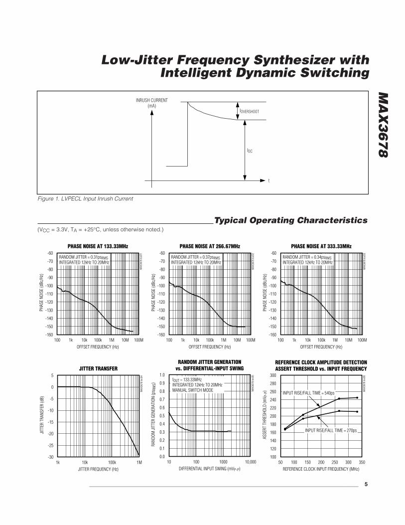
Figure 1. LVPECL Input Inrush Current
-150
-140
-130
-120
-110
-100
-90
-80
-70
-60
-160
PHASE NOISE AT 133.33MHz
MAX
3678
toc0
1
OFFSET FREQUENCY (Hz)
PHAS
E NO
ISE
(dBc
/Hz)
10M1M1k 10k 100k100 100M
RANDOM JITTER = 0.31psRMSINTEGRATED 12kHz TO 20MHz
-150
-140
-130
-120
-110
-100
-90
-80
-70
-60
-160
PHASE NOISE AT 266.67MHzM
AX36
78 to
c02
OFFSET FREQUENCY (Hz)
PHAS
E NO
ISE
(dBc
/Hz)
10M1M1k 10k 100k100 100M
RANDOM JITTER = 0.37psRMSINTEGRATED 12kHz TO 20MHz
-150
-140
-130
-120
-110
-100
-90
-80
-70
-60
-160
PHASE NOISE AT 333.33MHz
MAX
3678
toc0
3
OFFSET FREQUENCY (Hz)
PHAS
E NO
ISE
(dBc
/Hz)
10M1M1k 10k 100k100 100M
RANDOM JITTER = 0.34psRMSINTEGRATED 12kHz TO 20MHz
JITTER TRANSFER
MAX
3678
toc0
4
JITTER FREQUENCY (Hz)
JITTE
R TR
ANSF
ER (d
B)
100k10k
-25
-20
-15
-10
-5
0
5
-301k 1M
RANDOM JITTER GENERATIONvs. DIFFERENTIAL-INPUT SWING
MAX
3678
toc0
5
DIFFERENTIAL INPUT SWING (mVP-P)
RAND
OM JI
TTER
GEN
ERAT
ION
(ps R
MS)
1000100
0.1
0.2
0.3
0.4
0.5
0.6
0.7
0.8
0.9
1.0
0.010 10,000
fOUT = 133.33MHzINTEGRATED 12kHz TO 20MHzMANUAL SWITCH MODE
REFERENCE CLOCK AMPLITUDE DETECTIONASSERT THRESHOLD vs. INPUT FREQUENCY
MAX
3678
toc0
6
REFERENCE CLOCK INPUT FREQUENCY (MHz)
ASSE
RT T
HRES
HOLD
(mV P
-P)
300250200150100
120
140
160
180
200
220
240
260
280
300
10050 350
INPUT RISE/FALL TIME = 540ps
INPUT RISE/FALL TIME = 270ps
Typical Operating Characteristics(VCC = 3.3V, TA = +25°C, unless otherwise noted.)
MA
X3
67
8
Low-Jitter Frequency Synthesizer withIntelligent Dynamic Switching
6 _______________________________________________________________________________________
Typical Operating Characteristics (continued)(VCC = 3.3V, TA = +25°C, unless otherwise noted.)
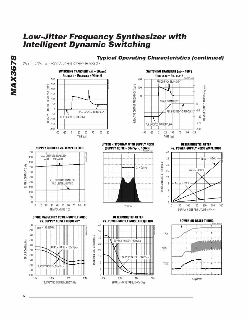
SWITCHING TRANSIENT (Δf = 50ppm)fREFCLK1 = (fREFCLK0 + 50ppm)
MAX
3678
toc0
7
TIME (μs)
RELA
TIVE
OUT
PUT
FREQ
UENC
Y (p
pm)
1007525 500-25
-150
-100
-50
0
50
100
150
200
250
300
-200-50 125
PLL LOCKED TO REFCLK0
PLL LOCKED TO REFCLK1
FREQUENCY TRANSIENT
PHASE TRANSIENT
SWITCHING TRANSIENT (Δφφ = 180°)(fREFCLK0 = fREFCLK1)
MAX3678 toc08
TIME (μs)RE
LATI
VE O
UTPU
T FR
EQUE
NCY
(ppm
)
RELA
TIVE
OUT
PUT
PHAS
E (d
egre
es)
1007550250-25
0
100
200
-180
-270
0
-90
-360-50 125
PLL LOCKED TO REFCLK1
PLL LOCKED TO REFCLK0
SUPPLY CURRENT vs. TEMPERATURE
MAX
3678
toc0
9
TEMPERATURE (°C)
SUPP
LY C
URRE
NT (m
A)
807050 6020 30 4010
50
100
150
200
250
300
350
400
450
500
00 90
ALL OUTPUTS ENABLEDAND TERMINATED
ALL OUTPUTS ENABLEDAND UNTERMINATED
JITTER HISTOGRAM WITH SUPPLY NOISE(SUPPLY NOISE = 50mVP-P, 100kHz)
MAX3678 toc10
2ps/div
DJ = 5psP-P
DETERMINISTIC JITTERvs. POWER-SUPPLY NOISE AMPLITUDE
MAX
3678
toc1
1
SUPPLY NOISE AMPLITUDE (mVP-P)
DETE
RMIN
ISTI
C JIT
TER
(ps P
-P)
25020050 100 150
5
10
15
20
25
30
35
40
00 300
fNOISE = 100kHz
fNOISE = 200kHz
fNOISE = 1MHz
SPURS CAUSED BY POWER-SUPPLY NOISEvs. SUPPLY NOISE FREQUENCY
MAX
3678
toc1
2
SUPPLY NOISE FREQUENCY (Hz)
SPUR
POW
ER (d
Bc)
1M100k
-90
-80
-70
-60
-50
-40
-30
-20
-10
0
-10010k 10M
fOUT = 133.33MHz
SUPPLY NOISE = 100mVP-P
SUPPLY NOISE = 50mVP-P
DETERMINISTIC JITTERvs. POWER-SUPPLY NOISE FREQUENCY
MAX
3678
toc1
3
SUPPLY NOISE FREQUENCY (Hz)
DETE
RMIN
ISTI
C JIT
TER
(ps P
-P)
1M100k
5
10
15
20
25
30
35
40
010k 10M
SUPPLY NOISE = 100mVP-P
SUPPLY NOISE = 50mVP-P
POWER-ON-RESET TIMINGMAX3678 toc14
200μs/div
VCC
OUTxx
LOCK
MA
X3
67
8
Low-Jitter Frequency Synthesizer withIntelligent Dynamic Switching
_______________________________________________________________________________________ 7
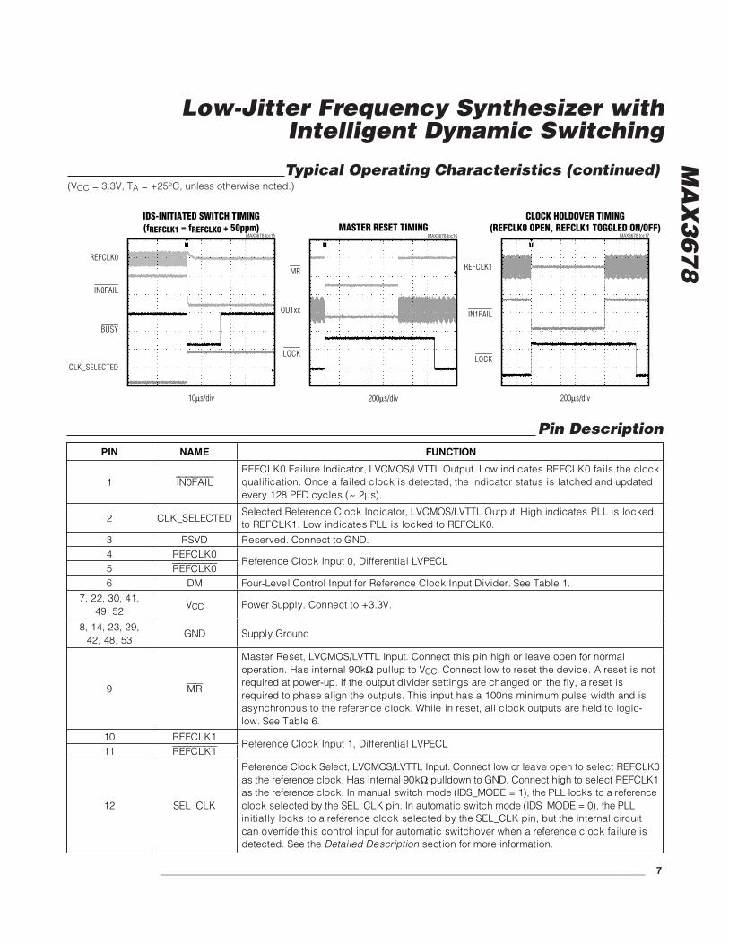
Pin DescriptionPIN NAME FUNCTION
1 IN0FAILREFCLK0 Failure Indicator, LVCMOS/LVTTL Output. Low indicates REFCLK0 fails the clock qualification. Once a failed clock is detected, the indicator status is latched and updated every 128 PFD cycles (~ 2μs).
2 CLK_SELECTED Selected Reference Clock Indicator, LVCMOS/LVTTL Output. High indicates PLL is locked to REFCLK1. Low indicates PLL is locked to REFCLK0.
3 RSVD Reserved. Connect to GND. 4 REFCLK0 5 REFCLK0
Reference Clock Input 0, Differential LVPECL
6 DM Four-Level Control Input for Reference Clock Input Divider. See Table 1.
7, 22, 30, 41, 49, 52
VCC Power Supply. Connect to +3.3V.
8, 14, 23, 29, 42, 48, 53
GND Supply Ground
9 MR
Master Reset, LVCMOS/LVTTL Input. Connect this pin high or leave open for normal operation. Has internal 90k pullup to VCC. Connect low to reset the device. A reset is not required at power-up. If the output divider settings are changed on the fly, a reset is required to phase align the outputs. This input has a 100ns minimum pulse width and is asynchronous to the reference clock. While in reset, all clock outputs are held to logic-low. See Table 6.
10 REFCLK1 11 REFCLK1
Reference Clock Input 1, Differential LVPECL
12 SEL_CLK
Reference Clock Select, LVCMOS/LVTTL Input. Connect low or leave open to select REFCLK0 as the reference clock. Has internal 90k pulldown to GND. Connect high to select REFCLK1 as the reference clock. In manual switch mode (IDS_MODE = 1), the PLL locks to a reference clock selected by the SEL_CLK pin. In automatic switch mode (IDS_MODE = 0), the PLL initially locks to a reference clock selected by the SEL_CLK pin, but the internal circuit can override this control input for automatic switchover when a reference clock failure is detected. See the Detailed Description section for more information.
IDS-INITIATED SWITCH TIMING(fREFCLK1 = fREFCLK0 + 50ppm)
MAX3678 toc15
10μs/div
REFCLK0
IN0FAIL
BUSY
CLK_SELECTED
MASTER RESET TIMINGMAX3678 toc16
200μs/div
MR
OUTxx
LOCK
CLOCK HOLDOVER TIMING(REFCLK0 OPEN, REFCLK1 TOGGLED ON/OFF)
MAX3678 toc17
200μs/div
REFCLK1
IN1FAIL
LOCK
Typical Operating Characteristics (continued)(VCC = 3.3V, TA = +25°C, unless otherwise noted.)
MA
X3
67
8
Low-Jitter Frequency Synthesizer withIntelligent Dynamic Switching
8 _______________________________________________________________________________________
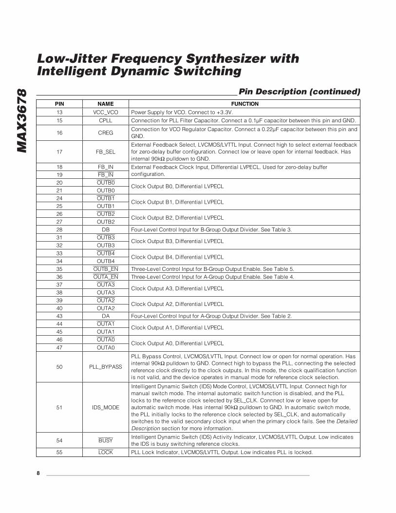
Pin Description (continued)PIN NAME FUNCTION
13 VCC_VCO Power Supply for VCO. Connect to +3.3V.
15 CPLL Connection for PLL Filter Capacitor. Connect a 0.1μF capacitor between this pin and GND.
16 CREG Connection for VCO Regulator Capacitor. Connect a 0.22μF capacitor between this pin and GND.
17 FB_SEL External Feedback Select, LVCMOS/LVTTL Input. Connect high to select external feedback for zero-delay buffer configuration. Connect low or leave open for internal feedback. Has internal 90k pulldown to GND.
18 FB_IN 19 FB_IN
External Feedback Clock Input, Differential LVPECL. Used for zero-delay buffer configuration.
20 OUTB021 OUTB0
Clock Output B0, Differential LVPECL
24 OUTB125 OUTB1
Clock Output B1, Differential LVPECL
26 OUTB227 OUTB2
Clock Output B2, Differential LVPECL
28 DB Four-Level Control Input for B-Group Output Divider. See Table 3. 31 OUTB332 OUTB3
Clock Output B3, Differential LVPECL
33 OUTB434 OUTB4
Clock Output B4, Differential LVPECL
35 OUTB_EN Three-Level Control Input for B-Group Output Enable. See Table 5. 36 OUTA_EN Three-Level Control Input for A-Group Output Enable. See Table 4. 37 OUTA338 OUTA3
Clock Output A3, Differential LVPECL
39 OUTA240 OUTA2
Clock Output A2, Differential LVPECL
43 DA Four-Level Control Input for A-Group Output Divider. See Table 2. 44 OUTA145 OUTA1
Clock Output A1, Differential LVPECL
46 OUTA047 OUTA0
Clock Output A0, Differential LVPECL
50 PLL_BYPASS
PLL Bypass Control, LVCMOS/LVTTL Input. Connect low or open for normal operation. Has internal 90k pulldown to GND. Connect high to bypass the PLL, connecting the selected reference clock directly to the clock outputs. In this mode, the clock qualification function is not valid, and the device operates in manual mode for reference clock selection.
51 IDS_MODE
Intelligent Dynamic Switch (IDS) Mode Control, LVCMOS/LVTTL Input. Connect high for manual switch mode. The internal automatic switch function is disabled, and the PLL locks to the reference clock selected by SEL_CLK. Connnect low or leave open for automatic switch mode. Has internal 90k pulldown to GND. In automatic switch mode, the PLL initially locks to the reference clock selected by SEL_CLK, and automatically switches to the valid secondary clock input when the primary clock fails. See the Detailed Description section for more information.
54 BUSYIntelligent Dynamic Switch (IDS) Activity Indicator, LVCMOS/LVTTL Output. Low indicates the IDS is busy switching reference clocks.
55 LOCK PLL Lock Indicator, LVCMOS/LVTTL Output. Low indicates PLL is locked.
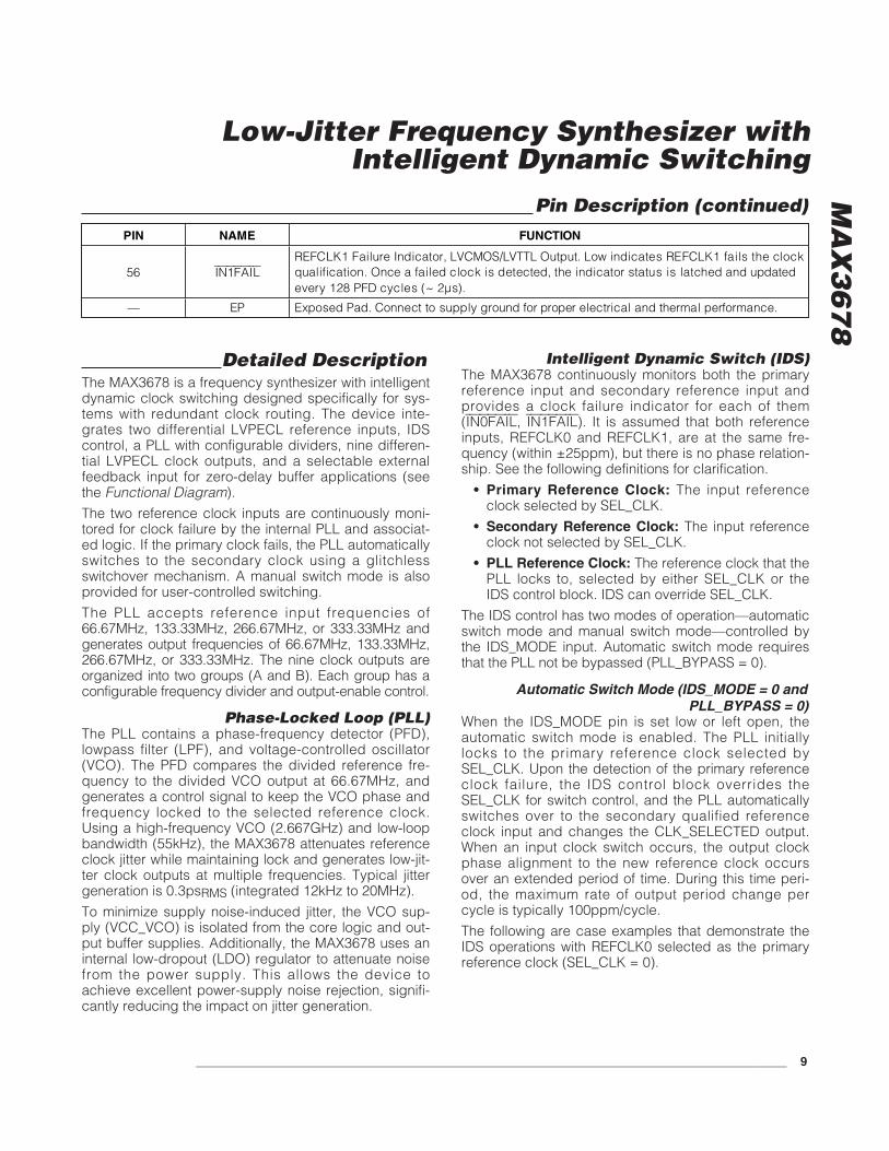
Detailed DescriptionThe MAX3678 is a frequency synthesizer with intelligentdynamic clock switching designed specifically for sys-tems with redundant clock routing. The device inte-grates two differential LVPECL reference inputs, IDScontrol, a PLL with configurable dividers, nine differen-tial LVPECL clock outputs, and a selectable externalfeedback input for zero-delay buffer applications (seethe Functional Diagram).
The two reference clock inputs are continuously moni-tored for clock failure by the internal PLL and associat-ed logic. If the primary clock fails, the PLL automaticallyswitches to the secondary clock using a glitchlessswitchover mechanism. A manual switch mode is alsoprovided for user-controlled switching.
The PLL accepts reference input frequencies of66.67MHz, 133.33MHz, 266.67MHz, or 333.33MHz andgenerates output frequencies of 66.67MHz, 133.33MHz,266.67MHz, or 333.33MHz. The nine clock outputs areorganized into two groups (A and B). Each group has aconfigurable frequency divider and output-enable control.
Phase-Locked Loop (PLL)The PLL contains a phase-frequency detector (PFD),lowpass filter (LPF), and voltage-controlled oscillator(VCO). The PFD compares the divided reference fre-quency to the divided VCO output at 66.67MHz, andgenerates a control signal to keep the VCO phase andfrequency locked to the selected reference clock.Using a high-frequency VCO (2.667GHz) and low-loopbandwidth (55kHz), the MAX3678 attenuates referenceclock jitter while maintaining lock and generates low-jit-ter clock outputs at multiple frequencies. Typical jittergeneration is 0.3psRMS (integrated 12kHz to 20MHz).
To minimize supply noise-induced jitter, the VCO sup-ply (VCC_VCO) is isolated from the core logic and out-put buffer supplies. Additionally, the MAX3678 uses aninternal low-dropout (LDO) regulator to attenuate noisefrom the power supply. This allows the device toachieve excellent power-supply noise rejection, signifi-cantly reducing the impact on jitter generation.
Intelligent Dynamic Switch (IDS)The MAX3678 continuously monitors both the primaryreference input and secondary reference input andprovides a clock failure indicator for each of them(IN0FAIL, IN1FAIL). It is assumed that both referenceinputs, REFCLK0 and REFCLK1, are at the same fre-quency (within ±25ppm), but there is no phase relation-ship. See the following definitions for clarification.
• Primary Reference Clock: The input referenceclock selected by SEL_CLK.
• Secondary Reference Clock: The input referenceclock not selected by SEL_CLK.
• PLL Reference Clock: The reference clock that thePLL locks to, selected by either SEL_CLK or theIDS control block. IDS can override SEL_CLK.
The IDS control has two modes of operation—automaticswitch mode and manual switch mode—controlled bythe IDS_MODE input. Automatic switch mode requiresthat the PLL not be bypassed (PLL_BYPASS = 0).
Automatic Switch Mode (IDS_MODE = 0 andPLL_BYPASS = 0)
When the IDS_MODE pin is set low or left open, theautomatic switch mode is enabled. The PLL initiallylocks to the primary reference clock selected bySEL_CLK. Upon the detection of the primary referenceclock failure, the IDS control block overrides theSEL_CLK for switch control, and the PLL automaticallyswitches over to the secondary qualified referenceclock input and changes the CLK_SELECTED output.When an input clock switch occurs, the output clockphase alignment to the new reference clock occursover an extended period of time. During this time peri-od, the maximum rate of output period change percycle is typically 100ppm/cycle.
The following are case examples that demonstrate theIDS operations with REFCLK0 selected as the primaryreference clock (SEL_CLK = 0).
MA
X3
67
8
Low-Jitter Frequency Synthesizer withIntelligent Dynamic Switching
_______________________________________________________________________________________ 9
Pin Description (continued)PIN NAME FUNCTION
56 IN1FAILREFCLK1 Failure Indicator, LVCMOS/LVTTL Output. Low indicates REFCLK1 fails the clock qualification. Once a failed clock is detected, the indicator status is latched and updated every 128 PFD cycles (~ 2μs).
— EP Exposed Pad. Connect to supply ground for proper electrical and thermal performance.
MA
X3
67
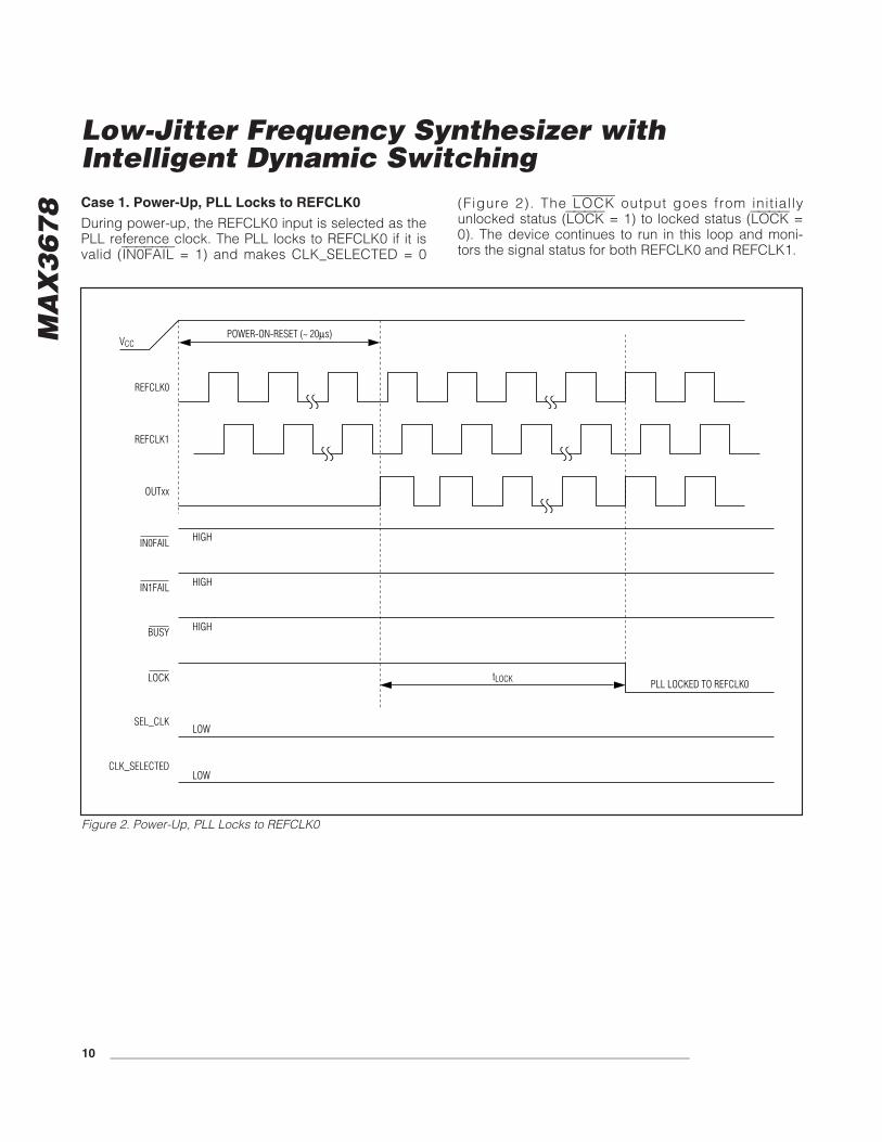
8 Case 1. Power-Up, PLL Locks to REFCLK0
During power-up, the REFCLK0 input is selected as thePLL reference clock. The PLL locks to REFCLK0 if it isvalid (IN0FAIL = 1) and makes CLK_SELECTED = 0
(Figure 2). The LOCK output goes from init ial lyunlocked status (LOCK = 1) to locked status (LOCK =0). The device continues to run in this loop and moni-tors the signal status for both REFCLK0 and REFCLK1.
Low-Jitter Frequency Synthesizer withIntelligent Dynamic Switching
10 ______________________________________________________________________________________
REFCLK0
REFCLK1
OUTxx
IN0FAIL
IN1FAIL
BUSY
LOCK
CLK_SELECTED
HIGH
SEL_CLKLOW
VCC
LOW
POWER-ON-RESET (~ 20μs)
HIGH
HIGH
tLOCK PLL LOCKED TO REFCLK0
Figure 2. Power-Up, PLL Locks to REFCLK0
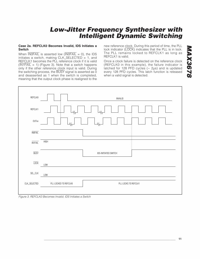
Case 2a. REFCLK0 Becomes Invalid, IDS Initiates aSwitch
When IN0FAIL is asserted low (IN0FAIL = 0), the IDSinitiates a switch, making CLK_SELECTED = 1, andREFCLK1 becomes the PLL reference clock if it is valid(IN1FAIL = 1) (Figure 3). Note that a switch happensonly if the other reference clock input is valid. Duringthe switching process, the BUSY signal is asserted as 0and deasserted as 1 when the switch is completed,meaning that the output clock phase is realigned to the
new reference clock. During this period of time, the PLLlock indicator (LOCK) indicates that the PLL is in lock.The PLL remains locked to REFCLK1 as long as REFCLK1 is valid.
Once a clock failure is detected on the reference clock(REFCLK0 in this example), the failure indicator islatched for 128 PFD cycles (~ 2µs) and is updatedevery 128 PFD cycles. This latch function is releasedwhen a valid signal is detected.
MA
X3
67
8
Low-Jitter Frequency Synthesizer withIntelligent Dynamic Switching
______________________________________________________________________________________ 11
REFCLK0
REFCLK1
OUTxx
IN0FAIL
IN1FAIL
BUSY
LOCK
CLK_SELECTED
INVALID
HIGH
IDS-INITIATED SWITCH
LOW
PLL LOCKED TO REFCLK0 PLL LOCKS TO REFCLK1
SEL_CLKLOW
Figure 3. REFCLK0 Becomes Invalid, IDS Initiates a Switch
MA
X3
67
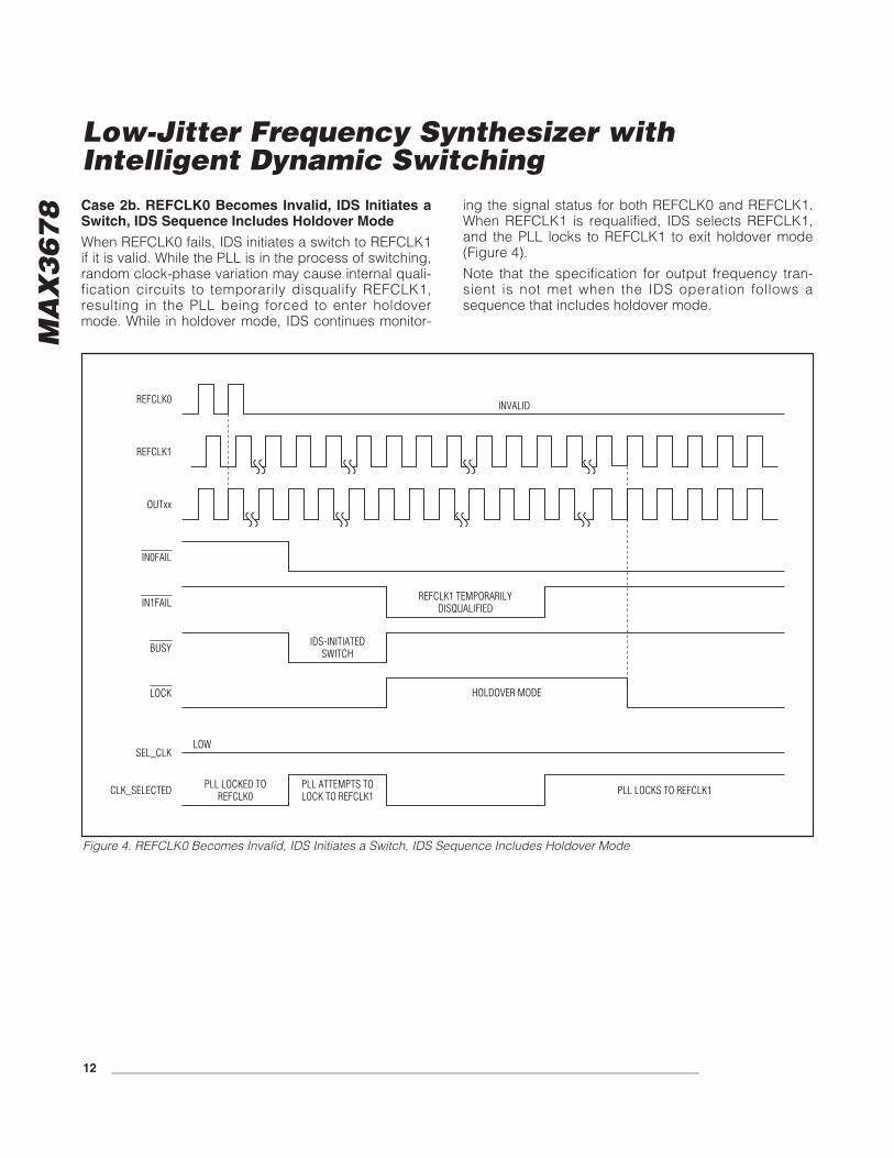
8 Case 2b. REFCLK0 Becomes Invalid, IDS Initiates aSwitch, IDS Sequence Includes Holdover Mode
When REFCLK0 fails, IDS initiates a switch to REFCLK1if it is valid. While the PLL is in the process of switching,random clock-phase variation may cause internal quali-fication circuits to temporarily disqualify REFCLK1,resulting in the PLL being forced to enter holdovermode. While in holdover mode, IDS continues monitor-
ing the signal status for both REFCLK0 and REFCLK1.When REFCLK1 is requalified, IDS selects REFCLK1,and the PLL locks to REFCLK1 to exit holdover mode(Figure 4).
Note that the specification for output frequency tran-sient is not met when the IDS operation follows asequence that includes holdover mode.
Low-Jitter Frequency Synthesizer withIntelligent Dynamic Switching
12 ______________________________________________________________________________________
REFCLK0
REFCLK1
OUTxx
CLK_SELECTED
INVALID
IN0FAIL
IN1FAIL
BUSY
LOCK
PLL LOCKED TOREFCLK0
PLL ATTEMPTS TOLOCK TO REFCLK1
SEL_CLK
PLL LOCKS TO REFCLK1
IDS-INITIATEDSWITCH
HOLDOVER MODE
LOW
REFCLK1 TEMPORARILYDISQUALIFIED
Figure 4. REFCLK0 Becomes Invalid, IDS Initiates a Switch, IDS Sequence Includes Holdover Mode
MA
X3
67
8
Low-Jitter Frequency Synthesizer withIntelligent Dynamic Switching
______________________________________________________________________________________ 13
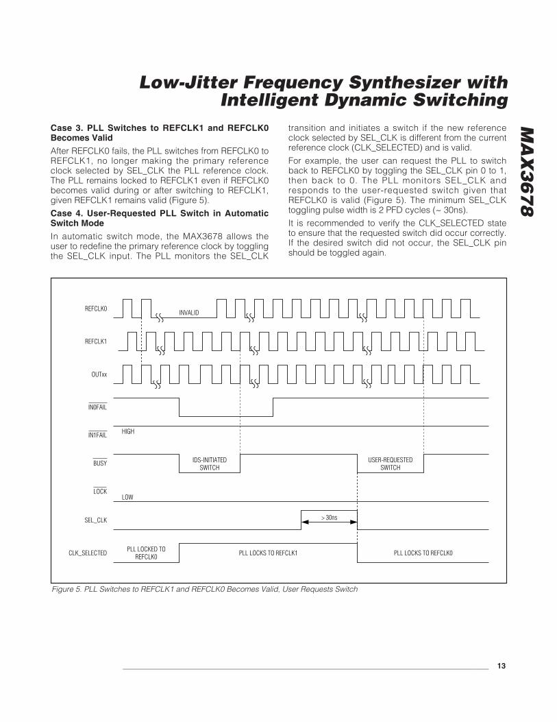
Case 3. PLL Switches to REFCLK1 and REFCLK0Becomes Valid
After REFCLK0 fails, the PLL switches from REFCLK0 toREFCLK1, no longer making the primary referenceclock selected by SEL_CLK the PLL reference clock.The PLL remains locked to REFCLK1 even if REFCLK0becomes valid during or after switching to REFCLK1,given REFCLK1 remains valid (Figure 5).
Case 4. User-Requested PLL Switch in AutomaticSwitch Mode
In automatic switch mode, the MAX3678 allows theuser to redefine the primary reference clock by togglingthe SEL_CLK input. The PLL monitors the SEL_CLK
transition and initiates a switch if the new referenceclock selected by SEL_CLK is different from the currentreference clock (CLK_SELECTED) and is valid.
For example, the user can request the PLL to switchback to REFCLK0 by toggling the SEL_CLK pin 0 to 1,then back to 0. The PLL monitors SEL_CLK andresponds to the user-requested switch given that REFCLK0 is valid (Figure 5). The minimum SEL_CLKtoggling pulse width is 2 PFD cycles (~ 30ns).
It is recommended to verify the CLK_SELECTED stateto ensure that the requested switch did occur correctly.If the desired switch did not occur, the SEL_CLK pinshould be toggled again.
REFCLK0
REFCLK1
OUTxx
IN0FAIL
IN1FAIL
BUSY
LOCK
CLK_SELECTED
INVALID
HIGH
LOW
PLL LOCKED TOREFCLK0 PLL LOCKS TO REFCLK1
SEL_CLK
PLL LOCKS TO REFCLK0
IDS-INITIATEDSWITCH
USER-REQUESTEDSWITCH
> 30ns
Figure 5. PLL Switches to REFCLK1 and REFCLK0 Becomes Valid, User Requests Switch
MA
X3
67
8
Low-Jitter Frequency Synthesizer withIntelligent Dynamic Switching
14 ______________________________________________________________________________________
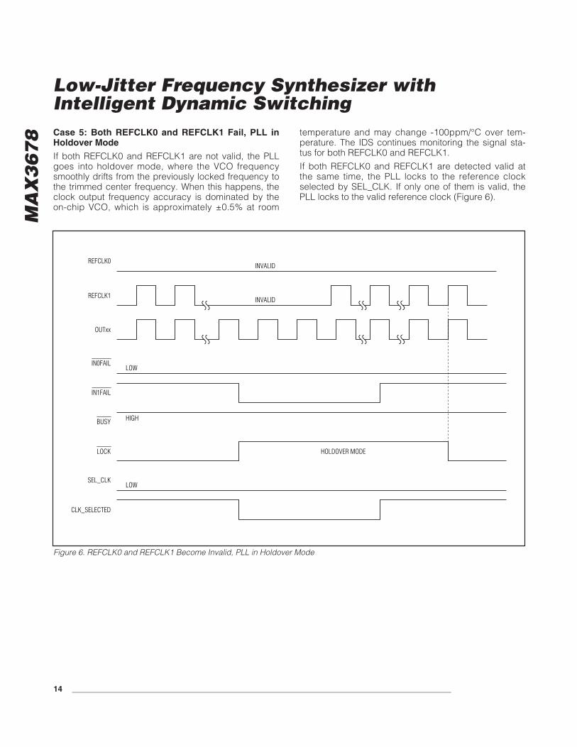
Case 5: Both REFCLK0 and REFCLK1 Fail, PLL inHoldover Mode
If both REFCLK0 and REFCLK1 are not valid, the PLLgoes into holdover mode, where the VCO frequencysmoothly drifts from the previously locked frequency tothe trimmed center frequency. When this happens, theclock output frequency accuracy is dominated by theon-chip VCO, which is approximately ±0.5% at room
temperature and may change -100ppm/°C over tem-perature. The IDS continues monitoring the signal sta-tus for both REFCLK0 and REFCLK1.
If both REFCLK0 and REFCLK1 are detected valid atthe same time, the PLL locks to the reference clockselected by SEL_CLK. If only one of them is valid, thePLL locks to the valid reference clock (Figure 6).
REFCLK0
REFCLK1
OUTxx
IN0FAIL
IN1FAIL
BUSY
LOCK
CLK_SELECTED
INVALID
SEL_CLKLOW
INVALID
HIGH
LOW
HOLDOVER MODE
Figure 6. REFCLK0 and REFCLK1 Become Invalid, PLL in Holdover Mode
MA
X3
67
8
Manual Switch Mode (IDS_MODE = 1)The manual switch mode is provided for user-controlledswitching. In manual switch mode, the PLL locks to areference clock selected by SEL_CLK. For example, ifSEL_CLK = 0, the PLL locks to REFCLK0 and forcesCLK_SELECTED = 0; if SEL_CLK is changed toSEL_CLK = 1, the PLL switches to REFCLK1 andmakes CLK_SELECTED = 1.
In manual switch mode, the IN0FAIL and IN1FAIL sta-tus indicators are still valid, but the manual-requestedswitch happens whether or not the selected referenceclock is valid.
Clock Failure ConditionsThe MAX3678 clock failure detection is performedusing the combination of amplitude qualification andPLL frequency and phase error qualification. The failurestatus is indicated for REFCLK0 and REFCLK1 atIN0FAIL and IN1FAIL, respectively. Once an indicatoris asserted low, it is latched and updated every 128PFD cycles (~ 2µs).
It should be noted that when the PLL is locked to a ref-erence clock, the clock failure indicator for the otherreference clock is only valid for amplitude qualificationand frequency qualification.
Amplitude QualificationA reference clock input fails amplitude qualification ifany of the following conditions occur:
A) Either one or both inputs (REFCLKx, REFCLKx)are shorted to VCC or GND.
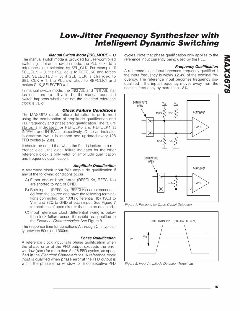
B) Both inputs (REFCLKx, REFCLKx) are disconnect-ed from the source and have the following termina-tions connected: (a) 100Ω differential, (b) 130Ω toVCC and 82Ω to GND at each input. See Figure 7for positions of open circuits that can be detected.
C) Input reference clock differential swing is belowthe clock failure assert threshold as specified inthe Electrical Characteristics. See Figure 8.
The response time for conditions A through C is typical-ly between 50ns and 300ns.
Phase QualificationA reference clock input fails phase qualification whenthe phase error at the PFD output exceeds the errorwindow (φerr) for more than 5 of 8 PFD cycles, as spec-ified in the Electrical Characteristics. A reference clockinput is qualified when phase error at the PFD output iswithin the phase error window for 8 consecutive PFD
cycles. Note that phase qualification only applies to thereference input currently being used by the PLL.
Frequency QualificationA reference clock input becomes frequency qualified ifthe input frequency is within ±2.4% of the nominal fre-quency. The reference input becomes frequency dis-qualified if the input frequency moves away from thenominal frequency by more than ±8%.
MAX3678130Ω
LVPECL
VCC
130Ω
82Ω 82Ω
VCCBOTH INPUTSOPEN
MAX3678
LVPECL100Ω
BOTH INPUTSOPEN
Figure 7. Positions for Open-Circuit Detection
0VVDT
DIFFERENTIAL INPUT: (REFCLKx - REFCLKx)
Figure 8. Input Amplitude Detection Threshold
Low-Jitter Frequency Synthesizer withIntelligent Dynamic Switching
______________________________________________________________________________________ 15
MA
X3
67
8
Low-Jitter Frequency Synthesizer withIntelligent Dynamic Switching
16 ______________________________________________________________________________________
PLL Out-of-Lock ConditionIf the frequency difference between the reference clockinput and the VCO at the PFD input becomes within500ppm, the PLL is considered to be in lock (LOCK =0). When the frequency difference between the refer-ence clock input and the VCO at the PFD inputbecomes greater than 800ppm, the PLL is consideredout-of-lock. It should be noted that the LOCK indicatoris not part of the frequency qualification used to initiateswitching between reference clocks.
Input and Output FrequenciesThe MAX3678 input and output dividers are configuredusing four-level control inputs DM, DA, and DB. Eachdivider is independent and can have a unique setting.The input connection and associated frequencies arelisted in Tables 1, 2, and 3.
Output-Enable ControlsEach output group (A and B) has a three-level controlinput OUTA_EN and OUTB_EN. See Tables 4 and 5 forconfiguration settings. When clock outputs are dis-abled, they are high impedance. Unused enabled out-puts should be left open.
Clock HoldoverIn automatic switch mode (IDS_MODE = 0), if bothREFCLK0 and REFCLK1 are not valid, the lock indica-tor deasserts (LOCK = 1) and the PLL goes intoholdover mode, where the VCO frequency smoothlydrifts from the previously locked frequency to thetrimmed center frequency. When this happens, theclock output frequency accuracy is dominated by the
Table 1. Divider M Configuration for InputFrequenciesCONNECTION FROM DM PIN INPUT FREQUENCY (MHz)
GND 66.67
VCC 133.33
Open 266.67
10k to GND 333.33
Table 2. Divider A Configuration for A-Group Output Frequencies
CONNECTION FROM DA PINOUTPUT FREQUENCY AT
OUTA[3:0] (MHz)
GND 66.67
VCC 133.33
Open 266.67
10k to GND 333.33
Table 3. Divider B Configuration for B-Group Output Frequencies
CONNECTION FROM DB PINOUTPUT FREQUENCY AT
OUTB[4:0] (MHz)
GND 66.67
VCC 133.33
Open 266.67
10k to GND 333.33
Table 4. OUTA[3:0] Enable Control
CONNECTION FROM OUTA_EN PIN A-GROUP OUTPUT ENABLEDA-GROUP OUTPUT DISABLED TO HIGH
IMPEDANCE
GND OUTA0, OUTA1, OUTA2, OUTA3 —
VCC* — OUTA0, OUTA1, OUTA2, OUTA3
Open OUTA0, OUTA1 OUTA2, OUTA3
Table 5. OUTB[4:0] Enable Control
CONNECTION FROM OUTB_EN PIN B-GROUP OUTPUT ENABLEDB-GROUP OUTPUT DISABLED TO HIGH
IMPEDANCE
GND OUTB0, OUTB1, OUTB2, OUTB3, OUTB4 —
VCC* OUTB0 OUTB1, OUTB2, OUTB3, OUTB4
Open OUTB0, OUTB1, OUTB2 OUTB3, OUTB4
*Connecting both OUTA_EN and OUTB_EN to VCC enables a factory test mode and forces all indicators to GND. This is not a validmode of operation.
*Connecting both OUTA_EN and OUTB_EN to VCC enables a factory test mode and forces all indicators to GND. This is not a validmode of operation.
MA
X3
67
8
on-chip VCO, which is approximately ±0.5% at roomtemperature and may change -100ppm/°C over tem-perature. While in holdover mode, IDS continues moni-toring the signal status for both REFCLK0 andREFCLK1 using amplitude and frequency qualification(phase qualification is not valid). The CLK_SELECTEDindicator is low and BUSY remains high. To exitholdover mode, at least one of the reference clocksmust be valid and selected as the PLL reference clock.
In manual switch mode (IDS_MODE = 1), if the select-ed reference clock is not valid, the PLL does not go intoholdover mode.
Power-On-Reset (POR)At power-on, an internal signal is generated to hold theMAX3678 in a reset state. This internal reset time isabout 20µs after VCC reaches 3.0V (Figure 2). Duringthe power-on-reset time, the outputs are held to logic-low (OUTxx = low and OUTxx = high). See Table 6 foroutput signal status during power-on-reset. After thisinternal reset time, the PLL starts to lock to the refer-ence clock selected by SEL_CLK.
Master ResetAfter power-up, an external master reset (MR) can beprovided to reset the internal dividers. This inputrequires a minimum reset pulse width of 100ns (activelow) and is asynchronous to the reference clock. WhileMR is low, all clock outputs are held to logic-low (OUTxx= low, OUTxx = high). See Table 6 for the output signalstatus during master reset. When the master reset inputis deasserted (MR = 1), the PLL starts to lock to the ref-erence clock selected by SEL_CLK.
Master reset is only needed for applications wheredivider configurations are changed on the fly and theclock outputs need to maintain phase alignment. Amaster reset is not required at power-up.
External Feedback for Zero-Delay BufferThe MAX3678 can be operated with either internal orexternal PLL feedback path, controlled by the FB_SELinput. Connecting FB_SEL to GND selects internalfeedback. For applications where a known phase rela-tionship between the reference clock input and theexternal feedback input (FB_IN, FB_IN) are needed forphase synchronization, connect FB_SEL to VCC forzero-delay buffer configuration and provide externalfeedback to the FB_IN input.
PLL Bypass ModePLL bypass mode is provided for test purposes. In thismode, the device receives two reference clocks to the2:1 mux, controlled by the SEL_CLK input. The select-ed primary reference clock is connected to the LVPECLclock outputs directly.
In PLL bypass mode (PLL_BYPASS = 1), the outputclock frequency is the same as the input clock frequen-cy. In this case, the clock amplitude and frequencyqualifications are still valid, but the phase qualificationis not available and the device is running in manualswitch mode.
BUSY IndicatorA BUSY signal is generated to indicate that the PLL isin the process of phase aligning to the new referenceclock. When BUSY = 0, the PLL is in switch mode;when BUSY = 1, the PLL operates normally.
Table 6. Output Signal Status During Power-On-Reset or Master Reset
OUTPUTDURING POWER-ON-RESET
(FOR ~ 20μs AFTER VCC > 3.0V)DURING MASTER RESET
(MR = 0)NOTES
CLK_SELECTED 0 —
IN0FAIL 1 Forced high regardless of reference input qualification.
IN1FAIL 1 Forced high regardless of reference input qualification.
LOCK 1 PLL out-of-lock.
BUSY 1 No switch happens.
OUTA[3:0] Logic-Low —
OUTB[4:0] Logic-Low —
Low-Jitter Frequency Synthesizer withIntelligent Dynamic Switching
______________________________________________________________________________________ 17
MA
X3
67
8
Low-Jitter Frequency Synthesizer withIntelligent Dynamic Switching
18 ______________________________________________________________________________________
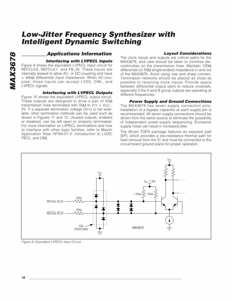
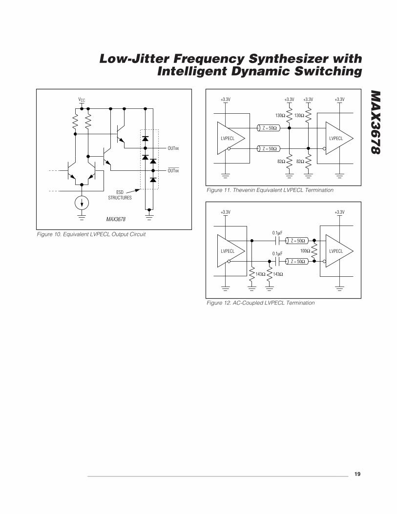
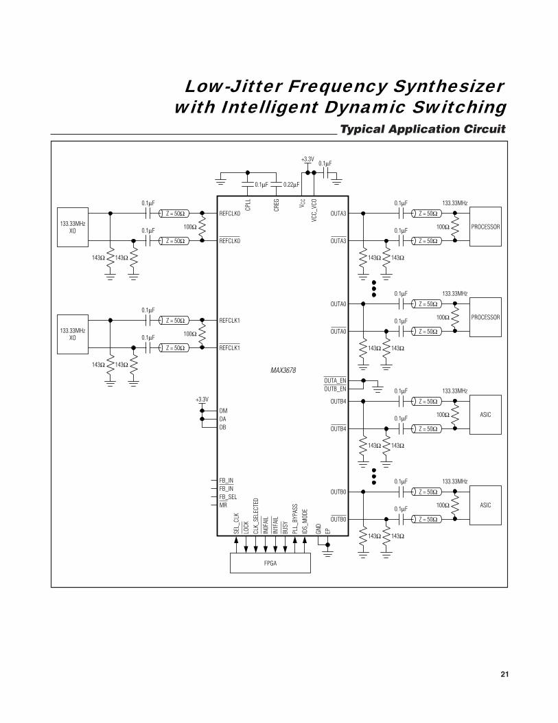
Applications InformationInterfacing with LVPECL Inputs
Figure 9 shows the equivalent LVPECL input circuit forREFCLK0, REFCLK1, and FB_IN. These inputs areinternally biased to allow AC- or DC-coupling and have> 40kΩ differential input impedance. When AC-cou-pled, these inputs can accept LVDS, CML, andLVPECL signals.
Interfacing with LVPECL OutputsFigure 10 shows the equivalent LVPECL output circuit.These outputs are designed to drive a pair of 50Ωtransmission lines terminated with 50Ω to VTT = VCC -2V. If a separate termination voltage (VTT) is not avail-able, other termination methods can be used such asshown in Figures 11 and 12. Unused outputs, enabledor disabled, can be left open or properly terminated.For more information on LVPECL terminations and howto interface with other logic families, refer to MaximApplication Note HFAN-01.0: Introduction to LVDS,PECL, and CML.
Layout ConsiderationsThe clock inputs and outputs are critical paths for theMAX3678, and care should be taken to minimize dis-continuities on the transmission lines. Maintain 100Ωdifferential (or 50Ω single-ended) impedance in and outof the MAX3678. Avoid using vias and sharp corners.Termination networks should be placed as close aspossible to receiving clock inputs. Provide spacebetween differential output pairs to reduce crosstalk,especially if the A and B group outputs are operating atdifferent frequencies.
Power Supply and Ground ConnectionsThe MAX3678 has seven supply connection pins;installation of a bypass capacitor at each supply pin isrecommended. All seven supply connections should bedriven from the same source to eliminate the possibilityof independent power-supply sequencing. Excessivesupply noise can result in increased jitter.
The 56-pin TQFN package features an exposed pad(EP), which provides a low-resistance thermal path forheat removal from the IC and must be connected to thecircuit board ground plane for proper operation.
ESDSTRUCTURES
REFCLKx, FB_IN
REFCLKx, FB_IN
VCC
VCC
VCC - 1.34V
MAX3678
> 20kΩ> 20kΩ200Ω
200Ω
Figure 9. Equivalent LVPECL Input Circuit
MA
X3
67
8
ESDSTRUCTURES
OUTxx
VCC
OUTxx
MAX3678
Figure 10. Equivalent LVPECL Output Circuit
82Ω
Z = 50Ω
Z = 50Ω
82Ω
130Ω 130Ω
+3.3V +3.3V+3.3V
LVPECLLVPECL
+3.3V
Figure 11. Thevenin Equivalent LVPECL Termination
143Ω
Z = 50Ω
Z = 50Ω
143Ω
LVPECLLVPECL 100Ω0.1μF
0.1μF
+3.3V +3.3V
Figure 12. AC-Coupled LVPECL Termination
Low-Jitter Frequency Synthesizer withIntelligent Dynamic Switching
______________________________________________________________________________________ 19
MA
X3
67
8
Low-Jitter Frequency Synthesizer withIntelligent Dynamic Switching
20 ______________________________________________________________________________________
Chip InformationTRANSISTOR COUNT: 28,366
PROCESS: BiCMOS
TOP VIEW
MAX3678
THIN QFN(8mm × 8mm × 0.8mm)
42 GNDIN0FAIL 1
41 VCCCLK_SELECTED 2
40 OUTA2RSVD 3
39 OUTA2REFCLK0 4
38 OUTA3REFCLK0 5
37 OUTA3DM 6
36 OUTA_ENVCC 7
35 OUTB_ENGND 8
34 OUTB4MR 9
33 OUTB4REFCLK1 10
32 OUTB3REFCLK1 11
31 OUTB3SEL_CLK 12
30 VCCVCC_VCO 13
29 GNDGND 14
15
56
CPLL
IN1F
AIL
16
55
CREG
LOCK
17
54
FB_S
ELBU
SY
18
53
FB_I
NGN
D
19
52
FB_I
NV C
C
20
51
OUTB
0ID
S_M
ODE
21
50
OUTB
0PL
L_BY
PASS
22
49
V CC
V CC
23
48
GND
GND
24
47
OUTB
1OU
TA0
25
46
OUTB
1OU
TA0
26
45
OUTB
2OU
TA1
27
44
OUTB
2OU
TA1
28
43
DBDA
EP*
*THE EXPOSED PAD OF THE TQFN PACKAGE MUST BE SOLDERED TO GROUND FOR PROPER THERMAL ANDELECTRICAL OPERATION.
Pin Configuration
.
PACKAGE TYPE PACKAGE CODE DOCUMENT NO.
56 TQFN-EP T5688+3 21-0135
For the latest package outline information and land patterns (footprints), go to http://www.microsemi.com
Package Information
MAX3678
REFCLK0
REFCLK0
OUTA3
CPLL
0.1μF
+3.3V0.1μF
CREG V C
C
VCC_
VCO
0.22μF
+3.3V
143Ω
Z = 50Ω
DM
OUTA_ENOUTB_EN
FB_INFB_IN
DADB
Z = 50Ω
143Ω
100Ω0.1μF
0.1μF
133.33MHzXO
143Ω
Z = 50Ω
Z = 50Ω
143Ω
OUTA3
100Ω0.1μF
0.1μF
PROCESSOR
PROCESSOR
133.33MHz
OUTA0
143Ω
Z = 50Ω
Z = 50Ω
143Ω
OUTA0
100Ω0.1μF
0.1μF
ASIC
ASIC
133.33MHz
OUTB4
143Ω
Z = 50Ω
Z = 50Ω
143Ω
OUTB4
100Ω0.1μF
0.1μF 133.33MHz
OUTB0
143Ω
Z = 50Ω
Z = 50Ω
143Ω
OUTB0
100Ω0.1μF
0.1μF 133.33MHz
FB_SELMR
REFCLK1
REFCLK1
143Ω
Z = 50Ω
Z = 50Ω
143Ω
100Ω0.1μF
0.1μF
133.33MHzXO
SEL_
CLK
LOCK
BUSY
PLL_
BYPA
SS
IDS_
MOD
E
CLK_
SELE
CTED
IN0F
AIL
IN1F
AIL
GND
EP
FPGA
Typical Application Circuit
Low-Jitter Frequency Synthesizer with Intelligent Dynamic Switching
� � 21

Microsemi Corporate Headquarters One Enterprise, Aliso Viejo CA 92656 USA Within the USA: +1 (949) 380-6100 Sales: +1 (949) 380-6136 Fax: +1 (949) 215-4996
Microsemi Corporation (NASDAQ: MSCC) offers a comprehensive portfolio of semiconductor solutions for: aerospace, defense and security; enterprise and communications; and industrial and alternative energy markets. Products include high-performance, high-reliability analog and RF devices, mixed signal and RF integrated circuits, customizable SoCs, FPGAs, and complete subsystems. Microsemi is headquartered in Aliso Viejo, Calif. Learn more at www.microsemi.com.
© 2012 Microsemi Corporation. All rights reserved. Microsemi and the Microsemi logo are trademarks of Microsemi Corporation. All other trademarks and service marks are the property of their respective owners.