1
The OPTICS IS LIGHT WORK column is an outgrowth of the OSA- sponsored Optical Fabrication and Testing Workshops. It is the intent of the Workshops to communicate technology and practice in the fields of optical manufacture and testing to opticians and optical engineers. Those attending the Workshops generally agree that the periodic meetings are fulfilling these goals; however, the audience that can be reached is small, perhaps 1200 people once a year. By publishing in Applied Optics a fabrication-and-test-oriented column, a far larger audience can be reached twelve times a year. This column is intended to be a means of timely exchange of specific tips or recipes to make the life of the optician or technician easier and more fruitful. Reports of experiences with new products and the ap- plication of familiar products in unique ways are encouraged. Transfers of other areas of technology to the solution of optical fabrication and testing problems would be welcomed. Material for this column is solicited from all workers in the field of optics and may be submitted to either editor. Limit your note to 500 words (2 double-spaced typed pages) and one illustration, just enough to get across one specific idea or method. Robert E. Parks Optical Sciences Center University of Arizona Tucson, Arizona 85721 Norman J. Brown Lawrence Livermore Laboratory Box 808 MS L-331 Livermore, California 94550 Low-cost electron-beam lithography package for the scanning electron microscope Brian L. Mcintyre and Christopher L. Dennis University of Rochester, NYS Center for Advanced Opti- cal Technology, Institute of Optics, Rochester, New York 14627. Received 1 December 1987. 0003-6935/88/020196-01$02.00/0. © 1987 Optical Society of America. For many years electron-beam lithography (or electron- beam writing) has been an important high-resolution fabri- cation technique, largely for photomask production in the semiconductor industry. The advantages inherent in this method center around the ability to finely focus electrons into a beam measured in hundreds or even tens of angstroms. Despite this resolution capability, the relative high cost of equipment required for electron-beam lithography has limit- ed its use as a general lithography tool. We found that the important electron-beam control func- tions, such as electron probe size, probe energy and current, probe position, and dwell time, exist (at some level) in many modern scanning electron microscopes. At the University of Rochester, we devised a mechanism to provide some of the basic functions of a high-cost e-beam tool at a more reason- able price, using equipment already found in many microsco- py facilities. We used a Tracor Northern x-ray analysis/ image analysis system and a Cambridge SEM to provide the basic lithography hardware. To fill the gap in system auto- mation, we authored a series of unique process control pro- grams that allow almost any SEM to be used as a submicron lithography tool. Incorporated into this system is a set of software libraries that allow digitization of the scanned area into a matrix of pixels, each individually addressable. Our application soft- ware was written in the Tracor Northern language FLEX- TRAN. The programs allow a setup of patterns in any of three unique modes: geometric specification (for squares, circles, etc.); mathematical specification (for curves and lines); and bit mapped graphics specification for patterns that are not easily defined otherwise. After setup, the pat- terns are then ported to the SEM for exposure of the sam- ples. We used the system described to fabricate submicron sur- face relief diffraction gratings in an electron resist material, as shown in Fig. 1. Overall pattern size is a function of the magnification of the SEM, which can be varied over a large range. The micrograph shows a portion of a grating with a period of -200 nm and an overall size of -0.25 mm 2 . This pattern was created in -20 min. The unique advantages of this system are two-fold. First, the way that pattern pixels are communicated to the micro- scope makes the fabrication of complex structures and Fig. 1. Grating in electron resist (period = 200 nm, depth = 100 nm). shapes as easy as simple geometric figures and greatly simpli- fies the combination of such features. Second, the spatial selectivity of this technique is demonstrated by the accuracy with which one can place the patterns on a substrate using the full resolution capability of the scanning electron micro- scope. We anticipate utilizing this new capability in the fabrication of a large variety of micro optical devices. This work was supported by the NYS Center for Advanced Optical Technology at The University of Rochester. 196 APPLIED OPTICS / Vol. 27, No. 2 / 15 January 1988

Low-cost electron-beam lithography package for the scanning electron microscope

Embed Size (px)

Citation preview

The OPTICS IS LIGHT WORK column is an outgrowth of the OSA-sponsored Optical Fabrication and Testing Workshops. It is the intentof the Workshops to communicate technology and practice in the fieldsof optical manufacture and testing to opticians and optical engineers.Those attending the Workshops generally agree that the periodicmeetings are fulfilling these goals; however, the audience that can bereached is small, perhaps 1200 people once a year. By publishing inApplied Optics a fabrication-and-test-oriented column, a far largeraudience can be reached twelve times a year.

This column is intended to be a means of timely exchange of specifictips or recipes to make the life of the optician or technician easier andmore fruitful. Reports of experiences with new products and the ap-plication of familiar products in unique ways are encouraged. Transfersof other areas of technology to the solution of optical fabrication andtesting problems would be welcomed.

Material for this column is solicited from all workers in the field ofoptics and may be submitted to either editor. Limit your note to 500words (2 double-spaced typed pages) and one illustration, just enoughto get across one specific idea or method.

Robert E. ParksOptical Sciences CenterUniversity of ArizonaTucson, Arizona 85721

Norman J. BrownLawrence Livermore LaboratoryBox 808 MS L-331Livermore, California 94550

Low-cost electron-beam lithography package for thescanning electron microscope

Brian L. Mcintyre and Christopher L. DennisUniversity of Rochester, NYS Center for Advanced Opti-cal Technology, Institute of Optics, Rochester, New York14627.Received 1 December 1987.0003-6935/88/020196-01$02.00/0.© 1987 Optical Society of America.For many years electron-beam lithography (or electron-

beam writing) has been an important high-resolution fabri-cation technique, largely for photomask production in thesemiconductor industry. The advantages inherent in thismethod center around the ability to finely focus electronsinto a beam measured in hundreds or even tens of angstroms.Despite this resolution capability, the relative high cost ofequipment required for electron-beam lithography has limit-ed its use as a general lithography tool.

We found that the important electron-beam control func-tions, such as electron probe size, probe energy and current,probe position, and dwell time, exist (at some level) in manymodern scanning electron microscopes. At the Universityof Rochester, we devised a mechanism to provide some of thebasic functions of a high-cost e-beam tool at a more reason-able price, using equipment already found in many microsco-py facilities. We used a Tracor Northern x-ray analysis/image analysis system and a Cambridge SEM to provide thebasic lithography hardware. To fill the gap in system auto-mation, we authored a series of unique process control pro-grams that allow almost any SEM to be used as a submicronlithography tool.

Incorporated into this system is a set of software librariesthat allow digitization of the scanned area into a matrix ofpixels, each individually addressable. Our application soft-ware was written in the Tracor Northern language FLEX-TRAN. The programs allow a setup of patterns in any ofthree unique modes: geometric specification (for squares,circles, etc.); mathematical specification (for curves andlines); and bit mapped graphics specification for patternsthat are not easily defined otherwise. After setup, the pat-terns are then ported to the SEM for exposure of the sam-ples.

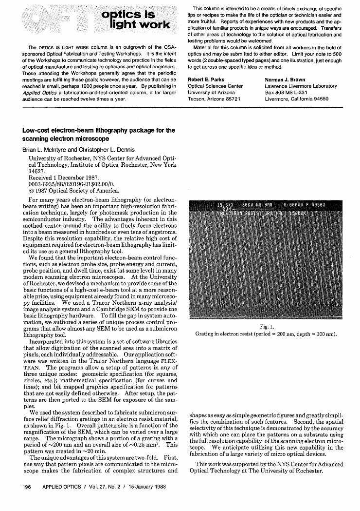
We used the system described to fabricate submicron sur-face relief diffraction gratings in an electron resist material,as shown in Fig. 1. Overall pattern size is a function of themagnification of the SEM, which can be varied over a largerange. The micrograph shows a portion of a grating with aperiod of -200 nm and an overall size of -0.25 mm2. Thispattern was created in -20 min.

The unique advantages of this system are two-fold. First,the way that pattern pixels are communicated to the micro-scope makes the fabrication of complex structures and

Fig. 1.Grating in electron resist (period = 200 nm, depth = 100 nm).

shapes as easy as simple geometric figures and greatly simpli-fies the combination of such features. Second, the spatialselectivity of this technique is demonstrated by the accuracywith which one can place the patterns on a substrate usingthe full resolution capability of the scanning electron micro-scope. We anticipate utilizing this new capability in thefabrication of a large variety of micro optical devices.

This work was supported by the NYS Center for AdvancedOptical Technology at The University of Rochester.

196 APPLIED OPTICS / Vol. 27, No. 2 / 15 January 1988