Embed Size (px)
Citation preview

General DescriptionThe MAX8664 dual-output PWM controller is a low-cost,high-performance solution for systems requiring dualpower supplies. It provides two individual outputs thatoperate 180° out-of-phase to minimize input currentripple, and therefore, capacitance requirements. Built-indrivers are capable of driving external MOSFETs todeliver up to 25A output current from each channel.The MAX8664 operates from a 4.5V to 28V input volt-age source and generates output voltages from 0.6Vup to 90% of the input voltage on each channel. Totaloutput regulation error is less than ±0.8% over load,line, and temperature.
The MAX8664 operates with a constant switching fre-quency adjustable from 100kHz to 1MHz. Built-in boostdiodes reduce external component count. Digital soft-start eliminates input inrush current during startup. Thesecond output has an optional external REFIN2, facili-tating tracking supply applications. Each output iscapable of sourcing and sinking current, making thedevice a great solution for DDR applications.
The MAX8664 employs Maxim’s proprietary peak volt-age-mode control architecture that provides superiortransient response during either load or line transients.This architecture is easily stabilized using two resistorsand one capacitor for any type of output capacitors. Fasttransient response requires less output capacitance,consequently reducing total system cost. The MAX8664Blatches off both controllers during a fault condition, whilethe MAX8664A allows one controller to continue to func-tion when there is a fault in the other controller.
ApplicationsDesktop and Notebook PCs
Graphic Cards
ASIC/CPU/DSP Power Supplies
Set-Top Box Power Supply
Printer Power Supply
Network Power Supply
POL Power Supply
Features� ±0.8% Output Accuracy Over Load and Line
� Operates from a Single 4.5V to 28V Supply
� Simple Compensation for Any Type of OutputCapacitor
� Internal 6.5V Regulator for Gate Drive
� Integrated Boost Diodes
� Adjustable Output from 0.6V to 0.9 x VIN
� Digital Soft-Start Reduces Inrush Current
� 100kHz to 1MHz Adjustable Switching
� 180° Out-of-Phase Operation Reduces InputRipple Current
� Overcurrent and Overvoltage Protection
� External Reference Input for Second Controller
� Prebiased Startup Operation
MA
X8
66
4
Low-Cost, Dual-Output, Step-DownController with Fast Transient Response
________________________________________________________________ Maxim Integrated Products 1
Ordering Information
19-0796; Rev 0; 4/07
For pricing delivery, and ordering information please contact Maxim Direct at 1-888-629-4642,or visit Maxim’s website at www.maxim-ic.com.
Note: This device operates over the -40°C to +85°C operating temperature range.
+Denotes lead-free package.
Pin Configuration appears at end of data sheet.
PART PIN-PACKAGE
PKGCODE
FAULTACTION
MAX8664AEEP+ 20 QSOP E20-1 Independent
MAX8664BEEP+ 20 QSOP E20-1 Joint
DH1
BST1
DL1
BST2
FB2 FB1
LX1
PGND
DH2
LX2
DL2
GND
IN1OUT2
IN2
OSC/EN12
ILIM2
PWRGDREFIN2
VCC
IN
ILIM1
VL
MAX8664
OUT1
Typical Operating Circuit
EVALUATION KIT
AVAILABLE

MA
X8
66
4
Low-Cost, Dual-Output, Step-DownController with Fast Transient Response
2 _______________________________________________________________________________________
ABSOLUTE MAXIMUM RATINGS
ELECTRICAL CHARACTERISTICS(VIN = 12V, ROSC/EN12 to GND = 56.1kΩ, REFIN2 = VCC, TA = -40°C to +85°C, unless otherwise noted. Typical values are at TA = +25°C.) (Note 2)
Stresses beyond those listed under “Absolute Maximum Ratings” may cause permanent damage to the device. These are stress ratings only, and functionaloperation of the device at these or any other conditions beyond those indicated in the operational sections of the specifications is not implied. Exposure toabsolute maximum rating conditions for extended periods may affect device reliability.
IN to GND ...........................................................…-0.3V to +30VVL to GND...................................................................-0.3 to +8VIN, BST_ to VL ........................................................-0.3V to +30VVCC, FB_, PWRGD to GND.......................................-0.3V to +6VVL to VCC....................................................................-2V to +8VPGND to GND .......................................................-0.3V to +0.6VDL_ to PGND...............................................-0.3V to (VVL + 0.3V)DH_ to PGND............................................-0.3V to (VBST_+ 0.3V)BST_ to GND.............................................................-0.3V to 38VBST_ to LX ................................................................-0.3V to +8VLX_ to PGND .................-1V (-2.5V for < 50ns transient) to +30VDH_ to LX_................................................-0.3V to (VBST_+ 0.3V)
ILIM_ to GND ...............................................-0.3V to (VIN + 0.3V)ILIM_ to LX_............................................................-0.6V to +30VOSC/EN12, REFIN2 to GND .....................-0.3V to (VVCC + 0.3V)VL Continuous Current ..............................................125mARMSVCC Continuous Current..............................................10mARMSContinuous Power Dissipation (TA = +70°C) (Note 1)
20-Pin QSOP (derate 11.0mW/°C above +70°C).........884mWOperating Temperature Range ...........................-40°C to +85°CJunction Temperature ......................................................+150°CStorage Temperature Range .............................-65°C to +150°CLead Temperature (soldering, 10s) .................................+300°C
PARAMETER CONDITIONS MIN TYP MAX UNITS
SUPPLY VOLTAGES
7.2 28.0IN Supply Voltage
IN = VL = VCC 4.5 5.5V
VL Output Voltage 7.2V < VIN < 28V, 0 < IVL < 60mA 6.10 6.6 6.75 V
VCC Output Voltage 7.2V < VIN < 28V, 0 < ICC < 5mA 4.5 5.0 5.5 V
Rising 3.4 3.5 3.6 VVCC Undervoltage Lockout(UVLO) Hysteresis 350 mV
VIN = 12V, IIN 0.095 0.2Standby Supply Current
OSC/EN12 notconnected VCC = VIN = VVL = 5V, IIN + IVL + IVCC 0.08 0.2
mA
VIN = 12V, IIN 1.4 2.5Operating Supply Current
No switching,VFB_ = 0.65V VCC = VIN = VVL = 5V, IIN + IVL+ IVCC 1.1 1.8
mA
REGULATOR SPECIFICATIONS
TA = 0°C to +85°C 0.5955 0.600 0.6045Reference Accuracy
TA = -40°C to +85°C 0.5930 0.600 0.6070V
TA = 0°C to +85°C 0.5952 0.600 0.6048VREFIN2 = VVCC
TA = -40°C to +85°C 0.5925 0.600 0.6075FB_ Regulation Accuracy
VREFIN2 = 1.000V 0.995 1.000 1.005
V
REFIN2 to Internal ReferenceSwitchover Threshold
Not to be switched during operation 2VVCC -
0.7VVCC -
0.3V
RE FIN 2 M axi m um P r og r am V ol tag e 1.3 V
REFIN2 Disable Threshold 50 mV
FB Input Bias Current VFB = 0.5V 3 nA
REFIN2 Bias Current VREFIN2 = 0.65V 3 nA
FB Propagation Delay FB rising to DH falling 90 ns
Note 1: Package mounted on a multilayer PCB.

MA
X8
66
4
Low-Cost, Dual-Output, Step-DownController with Fast Transient Response
_______________________________________________________________________________________ 3
PARAMETER CONDITIONS MIN TYP MAX UNITS
PROTECTION FEATURES
VFB1 rising 0.75Overvoltage Protection (OVP)Threshold VFB2 rising, VREFIN2 ≤ 1.3V
REFIN2+ 0.15
V
VREFIN2 = VVCC, VFB_ rising, MAX8664B
VFB1 rising, MAX8664A0.500 0.525 0.550 V
Power-Good (PWRGD) Threshold
Hysteresis 5 %
TA = +85oC 60High-Side Current-Sense ProgramCurrent (Note 3) TA = +25oC 44 50 60
µA
TA = +25°C 0.1 1.0ILIM Leakage
TA = +85°C 0.1µA
High-Side Current-SenseOvercurrent Trip Adjustment Range
0.05 0.40 V
Internal Soft-Start Time ROSC/EN12 = 56.1kΩ, 400kHz 2.5 ms
RE FIN 2 Inter nal P ul l d ow n Resi stance Engaged momentarily at startup 10 20 ΩThermal-Shutdown Threshold Junction temperature +160 °C
DRIVER SPECIFICATIONS
VVL = 6.5V 1.35 2.1Sourcing current,IDH = -50mA VIN = VVL = VVCC = 5V 1.55
VVL = 6.5V 0.9 1.4DH_ Driver Resistance
Sinking current,IDH = 50mA VIN = VVL = VVCC = 5V 1.0
Ω
VVL = 6.5V 1.3 2Sourcing current,IDL = -50mA VIN = VVL = VVCC = 5V 1.5
VVL = 6.5V 0.6 1.1DL_ Driver Resistance
Sinking current,IDL = 50mA VIN = VVL = VVCC = 5V 0.7
Ω
VVL = 6.5V 13 25 43Dead Time for Low-Side toHigh-Side Transition
DL_ falling to DH_ risingVVL = 5V 28
ns
DH_ Minimum On-Time 70 108 149 ns
VBST - VLX = 7V, VLX = 28V, VFB_ = 0.55V 1.25 2.3 mABST Current
OSC/EN12 not connected 0.001 µA
Internal Boost Switch Resistance 6 ΩPWM CLOCK OSCILLATOR
PWM Clock-Frequency Accuracy -15 +15 %
PWM Clock-Frequency AdjustmentRange
ROSC/EN12 = 226kΩ to 22.6kΩ 100 1000 kHz
OSC/EN12 Disable Current 1.5 2.5 µA
ELECTRICAL CHARACTERISTICS (continued)(VIN = 12V, ROSC/EN12 to GND = 56.1kΩ, REFIN2 = VCC, TA = -40°C to +85°C, unless otherwise noted. Typical values are at TA = +25°C.) (Note 2)
Note 2: Specifications at -40°C are guaranteed by design and not production tested.Note 3: This current linearly compensates for the MOSFET temperature coefficient.

MA
X8
66
4
Low-Cost, Dual-Output, Step-DownController with Fast Transient Response
4 _______________________________________________________________________________________
EFFICIENCY vs. LOAD CURRENT(600kHz, FIGURE 2)
MAX
8664
toc0
1
LOAD CURRENT (A)
EFFI
CIEN
CY (%
)
1
10
20
30
40
50
60
70
80
90
100
00.1 10
VOUT = 2.5V
VOUT = 1.8V
NO LOAD ON THEOTHER REGULATOR
EFFICIENCY vs. LOAD CURRENT(1MHz, FIGURE 4)
MAX
8664
toc0
2
LOAD CURRENT (A)
EFFI
CIEN
CY (%
)
1
10
20
30
40
50
60
70
80
90
100
00.1 10
VOUT1 = 2.5V
VOUT1 = 1.8V
VIN = 3.3VVVL = 5VNO LOAD ON OUT2
LOAD REGULATION(600kHz, FIGURE 2)
MAX
8664
toc0
3
OUT1 LOAD CURRENT (A)
OUT1
VOL
TAGE
(%)
2 4 6 8
2.46
2.47
2.48
2.49
2.50
2.51
2.52
2.53
2.54
2.55
2.450 10
IOUT2 = 8A IOUT2 = 4A
IOUT2 = 0A
POWER-UP WAVEFORMSMAX8664 toc08
VPRWGD
VOUT1
VOUT2
5V/div
2V/div
2V/div
10V/div
1ms/div
VIN
LINE REGULATION(600kHz, FIGURE 2)
MAX
8664
toc0
4
INPUT VOLTAGE (V)
OUT1
VOL
TAGE
(%)
8 10 12 14 1816
2.46
2.47
2.48
2.49
2.50
2.51
2.52
2.53
2.54
2.55
2.456 20
8A LOAD
NO LOAD
ROSC/EN12 vs. SWITCHING FRQUENCYM
AX86
64 to
c05
R OSC
/EN1
2 (kΩ
)
400 700
50
100
150
200
250
0100 1000
SWITCHING FREQUENCY (kHz)
OUT1 LOAD TRANSIENT (FIGURE 2)MAX8664 toc06
IOUT2
VOUT2
2A/div
100mV/div
20μs/div
2.5A 2.5A5A
LOAD TRANSIENT-3A TO +3A TO -3A (FIGURE 3)
MAX8664 toc07
IOUT2
VOUT1
VOUT2
5A/div
50mV/div
50mV/div
100μs/div
-3A -3A
+3A
Typical Operating Characteristics(Circuit of Figure 2, 600kHz, VIN = 12V, VOUT1 = 2.5V, VOUT2 = 1.8V, TA = +25°C, unless otherwise noted.)

MA
X8
66
4
Low-Cost, Dual-Output, Step-DownController with Fast Transient Response
_______________________________________________________________________________________ 5
POWER-DOWN WAVEFORMSMAX8664 toc09
VPRWGD
VOUT1
VOUT2
5V/div
2V/div
2V/div
10V/div
1ms/div
VIN
ENABLE WAVEFORMS (FIGURE 2)MAX8664 toc10
VPRWGD
VOUT1
VOUT2
5V/div
5V/div
2V/div
2V/div
1ms/div
ENABLE
ENABLE WAVEFORMS (FIGURE 4)MAX8664 toc11
VPRWGD
VOUT1
VOUT2
5V/div
5V/div
1V/div
1V/div
400μs/div
ENABLE
SWITCHING WAVEFORMSMAX8664 toc12
IL1
IL2
10V/div
10V/div
5A/div
5A/div
2μs/div
VLX1
VLX2
FEEDBACK VOLTAGEvs. TEMPERATURE
MAX
8664
toc1
3
FEED
BACK
VOL
TAGE
(mV)
0 40
597
596
599
601
603
598
600
602
604
605
595-40 100-20 20 8060
TEMPERATURE (°C)
NO LOAD
SHORT-CIRCUIT WAVEFORMSMAX8664 toc14
IL1
IIN
5A/div
2V/div
2A/div
5V/div10μs/div
VOUT1
VPRWGD
OVERVOLTAGE PROTECTIONMAX8664 toc15
VDH1
IL1
10V/div
5V/div
10A/div
10V/div
20μs/div
VOUT1
VDL1
Typical Operating Characteristics (continued)(Circuit of Figure 2, 600kHz, VIN = 12V, VOUT1 = 2.5V, VOUT2 = 1.8V, TA = +25°C, unless otherwise noted.)
MA
X8
66
4
Low-Cost, Dual-Output, Step-DownController with Fast Transient Response
6 _______________________________________________________________________________________
Pin Description
PIN NAME FUNCTION
1 DH1High-Side MOSFET Driver Output for Controller 1. Connect DH1 to the gate of the high-side MOSFET. DH1 islow in shutdown and UVLO.
2 LX1External Inductor Connection for Controller 1. Connect LX1 to the switching node of the MOSFETs andinductor. Make sure LX1 is close to the source of the high-side MOSFET(s) to form a Kelvin connection forhigh-side current sensing. LX1 is high impedance during monotonic startup and shutdown.
3 BST1Boost Capacitor Connection for the High-Side MOSFET Driver for Controller 1. Connect a 0.22µF ceramiccapacitor from BST1 to LX1.
4 DL1Low-Side MOSFET Driver Output for Controller 1. Connect DL1 to the gate of the low-side MOSFET(s) forcontroller 1. DL1 is low in shutdown and UVLO.
5 VLLow-Side Gate Drive Supply and Output of the 6.5V Linear Regulator. Connect a 4.7µF ceramic capacitor fromVL to PGND. When using a 4.5V to 5.5V supply, connect VL to IN. VL is the input to the VCC supply. Do notload VL when IC is disabled.
6 PGNDPower Ground. Connect to the power ground plane. Connect power and analog grounds at a single point nearthe output capacitor’s ground.
7 DL2Low-Side MOSFET Driver Output for Controller 2. Connect DL2 to the gate of the low-side MOSFET(s) forcontroller 2. DL2 is low in shutdown and UVLO.
8 BST2Boost Capacitor Connection for the High-Side MOSFET Driver for Controller 2. Connect a 0.22µF ceramiccapacitor from BST2 to LX2.
9 LX2External Inductor Connection for Controller 2. Connect LX2 to the switching node of the MOSFETs andinductor. Make sure LX2 is close to the source of the high-side MOSFET(s) to form a Kelvin connection forhigh-side current sensing. LX2 is high impedance during monotonic startup and shutdown.
10 DH2High-Side MOSFET Driver Output for Controller 2. Connect DH2 to the gate of the high-side MOSFET(s) forcontroller 2. DH2 is low in shutdown and UVLO.
11 ILIM2Current-Limit Set for Controller 2. Connect a resistor from the drain of the high-side MOSFET(s) to ILIM2. Seethe Setting the Overcurrent Threshold section.
12 FB2Feedback Input for Controller 2. Connect FB2 to the center of a resistor-divider connected between the outputof controller 2 and GND to set the desired output voltage. VFB2 regulates to VREFIN2 or the internal 0.6Vreference. To use the internal reference, connect REFIN2 to VCC.
13 REFIN2
External Reference Input for Controller 2. To use the internal 0.6V reference, connect REFIN2 to VCC. To usean external reference, connect REFIN2 through a resistor (> 1kΩ) to a reference voltage between 0V and1.3V. An RC lowpass filter is recommended when using an external reference and soft-start is not provided bythe external reference. For tracking applications, connect REFIN2 to the center of a resistor voltage-dividerbetween the output of controller 1 and GND (see Figure 3). Connect REFIN2 to GND to disable controller 2.
14 OSC/EN12
Switching Frequency Set Input. Connect a 22.6kΩ to 226kΩ resistor from OSC/EN12 to GND to set theswitching frequency between 1000kHz and 100kHz. Connect a switch in series with this resistor forenable/shutdown control. When the switch is open, the IC enters low-power shutdown mode. In shutdown,OSC/EN12 is internally driven to approximately 800mV.
15 INInternal 6.5V Linear Regulator Input. Connect IN to a 7.2V to 28V supply, and connect a 0.47µF or largerceramic capacitor from IN to PGND. When using a 4.5V to 5.5V supply, connect IN to VL.
16 GNDAnalog Ground. Connect to the analog ground plane. Connect the analog and power ground planes at asingle point near the output capacitor’s ground.

MA
X8
66
4
Low-Cost, Dual-Output, Step-DownController with Fast Transient Response
_______________________________________________________________________________________ 7
Pin Description (continued)
PIN NAME FUNCTION
17 VCC
Internal Analog Supply. VCC regulates to 1.5V below VVL. Connect a 1µF ceramic capacitor from VCC to GND.When using a 4.5V to 5.5V supply, connect a 10Ω resistor from VCC to IN. VCC is used to power the IC’sinternal circuitry.
18 PWRGD
Open-Drain Power-Good Output. PWRGD is high impedance when controllers 1 and 2 (using the internalreference) are in regulation. PWRGD is low if the outputs are out of regulation, if there is a fault condition, or ifthe IC is shut down. PWRGD does not reflect the status of output 2 in the MAX8664A or when REFIN2 isconnected to an external reference in the MAX8664B.
19 FB1Feedback Input for Controller 1. Connect FB1 to the center of a resistor-divider connected between the outputof controller 1 and GND to set the desired output voltage. VFB1 regulates to 0.6V.
20 ILIM1Current-Limit Set for Controller 1. Connect a resistor from the drain of the high-side MOSFET(s) to ILIM1. Seethe Setting the Overcurrent Threshold section.

MA
X8
66
4
Low-Cost, Dual-Output, Step-DownController with Fast Transient Response
8 _______________________________________________________________________________________
CONTROLLOGIC
CONTROLLOGIC
THERMALSHUTDOWN
THERMALSHUTDOWN
VOLTAGEREFERENCE
BIASGENERATOR
OSCILLATOR
SHUTDOWNCONTROL
LOGIC
UVLOCIRCUITRY
FB1
REF1 - 0.1V
VCC
REFIN2
OSC/EN12
PGND
LX1
ILIM1
BST1
PWMCOMPARATOR 1
PWMCOMPARATOR 2
BST CAPCHARGING SWITCH
BST CAPCHARGING SWITCH
CURRENT-LIMITCOMPARATOR
CURRENT-LIMITCOMPARATOR
LX1
IF VREFIN2 > 2.0VOPEN S1 AND CLOSE S2.OTHERWISE, CLOSE S1
AND OPEN S2.
VL
LX2
ILIM2
BST2
SOFT-START 1
FB2
0.6V
REF
CLOCK 1
DL1
50μA
50μA
DH1
DH2
DL2
LX2
FB1
IN VL
VCCGND
FB2
REF2 - 0.1V
6.5V LDO
PWRGD4μA
S2
REF2
REF EN
SHUTDOWN 1
SHUTDOWN 1
CLOCK 2
CLOCK 1
CLOCK 2
SOFT-START
SHUTDOWN 2
SHUTDOWN 2
REF
THERMALSHUTDOWN
EN
S1
50mV
ENABLE2
ENABLE
1.5V
Figure 1. Functional Diagram

MA
X8
66
4
Low-Cost, Dual-Output, Step-DownController with Fast Transient Response
_______________________________________________________________________________________ 9
Detailed DescriptionThe MAX8664 dual-output PWM controller is a low-costsolution for dual power-supply systems. It provides twoindividual outputs that operate 180° out-of-phase tominimize input capacitance requirements. Built-in dri-vers are capable of driving external MOSFETs to deliv-er up to 25A of current from each output. The MAX8664operates from a 4.5V to a 5.5V or a 7.2V to 28V inputand generates output voltages from 0.6V up to 90% ofthe input voltage on each channel. Total output error isless than ±0.8% over load, line, and temperature.
The MAX8664 operates with a constant switching fre-quency adjustable from 100kHz to 1MHz. Built-in boostdiodes reduce external component count. Digital soft-start eliminates input inrush current during startup. Thesecond output has an optional REFIN2 input that takesan external reference voltage, facilitating tracking supplyapplications. Each output is capable of sourcing andsinking current. Internal 6.5V and 5V linear regulatorsprovide power for gate drive and internal IC functions.The MAX8664 has built-in protection against output over-voltage, overcurrent, and thermal faults. The MAX8664Blatches off both controllers during a fault condition, whilethe MAX8664A allows one controller to continue to func-tion when there is a fault in the other controller.
The MAX8664 employs Maxim’s proprietary peak-volt-age mode control architecture that provides superiortransient response during either load or line transients.This architecture is easily stabilized using two resistorsand one capacitor for any type of output capacitors.Fast transient response requires less output capaci-tance, consequently reducing total system cost.
DC-DC Controller ArchitectureThe peak-voltage mode PWM control scheme ensuresstable operation, simple compensation for any outputcapacitor, and fast transient response. An on-chip inte-grator removes any DC error due to the ripple voltage.This control scheme is simple: when the output voltagefalls below the regulation threshold, the error compara-tor begins a switching cycle by turning on the high-sideswitch at the rising edge of the following clock cycle.This switch remains on until the minimum on-timeexpires and the output voltage is in regulation or thecurrent-limit threshold is exceeded. At this point, thelow-side synchronous rectifier turns on and remains onuntil the rising edge of the first clock cycle after the out-put voltage falls below the regulation threshold.
Internal Linear RegulatorsThe internal VL low-dropout linear regulator of theMAX8664A and MAX8664B provides the 6.5V supplyused for the gate drive. Connect a 4.7µF ceramiccapacitor from VL to PGND. When using a 4.5V to 5.5Vinput supply, connect VL directly to IN.
The 5V supply used to power IC functions (VCC) is gen-erated by an internal 1.5V shunt regulator from VL.Connect a 2.2µF ceramic capacitor from VCC to GND.When using a 4.5V to 5.5V input supply, connect VCCto IN through a 10Ω resistor.
High-Side Gate-Drive Supply (BST_)The gate-drive voltage for the high-side MOSFETs isgenerated using a flying capacitor boost circuit. Thecapacitor between BST_ and LX_ is charged to the VLvoltage through the integrated BST_ diode during thelow-side MOSFET on-time. When the low-side MOSFETis switched off, the BST_ voltage is shifted above theLX_ voltage to provide the necessary turn-on voltage(VGS) for the high-side MOSFET. The controller closesa switch between BST_ and DH_ to turn the high-sideMOSFET on.
Voltage ReferenceAn internal 0.6V reference sets the feedback regulationvoltage. Controller 1 always uses the internal reference.An external reference input is provided for controller 2.To use the external reference, connect a 0 to 1.3V sup-ply to REFIN2. This facilitates tracking applications. Touse the internal 0.6V reference for controller 2, connectREFIN2 to VCC.
Undervoltage Lockout (UVLO)When the VCC supply voltage drops below the UVLOthreshold (3.15V falling typ), the undervoltage lockout(UVLO) circuitry inhibits the switching of both con-trollers, and forces the DL and DH gate drivers low.When VCC rises above the UVLO threshold (3.5V risingtyp), the controllers begin the startup sequence andresume normal operation.
Output Overcurrent ProtectionWhen the MAX8664 detects an overcurrent condition,DH is immediately pulled low. If the overcurrent conditionpersists for four consecutive cycles, the controller latch-es off and both DH_ and DL_ are pulled low. During soft-start, when FB_ is less than 300mV, the controller latchesoff on the first overcurrent condition. The protection cir-cuit detects an overcurrent condition by sensing thedrain-source voltage across the high-side MOSFET(s).

MA
X8
66
4
Low-Cost, Dual-Output, Step-DownController with Fast Transient Response
10 ______________________________________________________________________________________
The threshold that trips overcurrent protection is set by aresistor connected from ILIM_ to the drain of the high-side MOSFET(s). ILIM_ sinks 50µA (typ) through thisresistor. When the drain-source voltage exceeds the volt-age drop across this resistor during the high-side MOSFET(s) on-time, an overcurrent fault is triggered. Toprevent glitches from falsely tripping the overcurrent pro-tection, connect a filter capacitor (0.01µF typically) inparallel with the overcurrent-setting resistor.
Output Overvoltage Protection (OVP)During an overvoltage event on one or both of its out-puts, the MAX8664 latches off the controller. Thisoccurs when the feedback voltage exceeds its normalregulation voltage by 150mV for 10µs. In this state, thelow-side MOSFET(s) are on and the high-side MOS-FET(s) are off to discharge the output. To clear thelatch, cycle EN or the input power.
Thermal-Overload ProtectionThermal-overload protection limits total power dissipa-tion in the MAX8664. When the junction temperatureexceeds +160°C, an internal thermal sensor shuts downthe device, pulling DH_ and DL_ low for both controllers.To restart the controller, cycle EN or input power.
Power-Good Output (PWRGD)PWRGD is an open-drain output that is pulled low whenthe output voltage rises above the PWRGD upperthreshold or falls below the PWRGD falling threshold.PWRGD is held low in shutdown, when VCC is below theUVLO threshold, during soft-start, and during fault con-ditions. PWRGD does not reflect the status of controller2 in the MAX8664A, or when REFIN2 is connected to anexternal reference with either version. See Table 1 forPWRGD operation of the circuits of Figures 2–5 duringfault conditions. For logic-level output voltages, con-nect an external pullup resistor between PWRGD andthe logic power supply. A 100kΩ resistor works well inmost applications.
Fault-Shutdown ModesWhen an overvoltage or overcurrent fault occurs on onecontroller of the MAX8664A, the second controller con-tinues to operate. With the MAX8664B, a fault in onecontroller latches off both controllers automatically, andPWRGD is pulled low. See Table 1 for the fault-shut-down modes of the circuits shown in Figures 2–5.
Table 1. Fault Shutdown Modes for Circuits of Figures 2–5MAX8664A (INDEPENDENT) MAX8664B (JOINT)
CIRCUITCONTROLLER 1 FAULT CONTROLLER 2 FAULT CONTROLLER 1 FAULT CONTROLLER 2 FAULT
Figure 2,Figure 5(Independent)
Controller 2 remains on.PWRGD is pulled low.
Controller 1 remains on.PWRGD remains high.
Controller 2 is shut down.PWRGD is pulled low.
Controller 1 is shut down.PWRGD is pulled low.
Figure 3(Tracking)
Controller 2 shuts down.PWRGD is pulled low.
Controller 1 remains on.PWRGD remains high.
Controller 2 is shut down.PWRGD is pulled low.
Controller 1 is shut down.PWRGD is pulled low.
Figure 4(Sequenced)
Controller 2 shuts down.PWRGD is pulled low.
Controller 1 remains on.PWRGD remains high.
Controller 2 is shut down.PWRGD is pulled low.
Controller 1 is shut down.PWRGD is pulled low.

MA
X8
66
4
Low-Cost, Dual-Output, Step-DownController with Fast Transient Response
______________________________________________________________________________________ 11
MAX8664
ILIM1
C2010μF
DH1C171μF
C181μF
LX1
BST1
DL1
PGND
ILIM2
DH2
LX2
BST2ENABLE
ONOFF DL2
FB1
IN
INPUT10.8V TO 13.2V
POWER-GOODTO SYSTEM
VCC
C190.01μF
N1
R351.1kΩ
L1 1μH
R43.92kΩ
R51.15kΩ
C51500pF
OUT12.5V/8A
N2
R12.7kΩ
R1039.2kΩ
VCC
REFIN2
VL
C130.22μF
C25680pF
R373Ω
GND
PWRGD
R910kΩ
N92N7002
OSC/EN12
FB2
C144.7μF
C110μF
C41000μF
C230.1μF
C847μF
C747μF
C647μF
C2110μF
C160.01μF
N3
R73.92kΩ
R383Ω
C26680pF R8
1.82kΩ
L2 1μH
R651.1kΩ
C121500μF
OUT21.8V/8A
N4
R23.01kΩ
C150.22μF
C310μF
C220.1μF
C1147μF
C1047μF
C947μF
C270.47μF
Figure 2. Low-Cost, 600kHz Typical Application Circuit

MA
X8
66
4
Low-Cost, Dual-Output, Step-DownController with Fast Transient Response
12 ______________________________________________________________________________________
Table 2. Component List for Figure 2DESIGNATION QTY DESCRIPTION
C1, C3,C20, C21
410µF ±20%, 16V X5R ceramiccapacitors (1206)
C4 11000µF ±20%, 16V electrolyticcapacitor (8mm diameter,20mm height)
C5, C12 21500pF, 50V C0G ceramiccapacitors (0603)
C6–C11 647µF ±20%, 6.3V X5R ceramiccapacitors (1206)
C13, C15 20.22µF ±10%, 25V X7R ceramiccapacitors (0603)
C14 14.7µF ±10%, 6.3V X5R ceramiccapacitor (0805)
C16, C19 20.01µF ±10%, 50V X7R ceramiccapacitors (0603)
C17 11µF ±20%, 16V X5R ceramiccapacitor (0603)
C18 11µF ±20%, 6.3V X5R ceramiccapacitor (0603)
C22, C23 20.1µF ±20%, 16V X7R ceramiccapacitors (0603)
DESIGNATION QTY DESCRIPTION
C25, C26 2680pF, 50V C0G ceramic capacitors(0603)
C27 10.47µF ±10%, 16V ceramiccapacitor (0603)
L1, L2 21µH inductorsTOKO FDV0630-1R0M
N1–N4 4n-channel MOSFETs (8-pin SO)International Rectifier IRF7821
N9 1n-channel MOSFET (SOT23)Central 2N7002
R1 1 2.74kΩ ±1% resistor (0603)
R2 1 301kΩ ±1% resistor (0603)
R3, R6 2 51.1kΩ ±1% resistors (0603)
R4, R7 2 3.92kΩ ±1% resistors (0603)
R5 1 1.15kΩ ±1% resistor (0603)
R8 1 1.82kΩ ±1% resistor (0603)
R9 1 10kΩ ±5% resistor (0603)
R10 1 39.2kΩ ±1% resistor (0603)
R37, R38 2 3Ω ±5% resistors (0805)
U1 1 MAX8664 (20-pin QSOP)

MA
X8
66
4
Low-Cost, Dual-Output, Step-DownController with Fast Transient Response
______________________________________________________________________________________ 13
FB1
IN
PWRGD
VCC
VL
GND
OSC/EN12
REFIN2
ILIM2
FB2
ILIM1
DH1
LX1
BST1
DL1
PGND
DH2
LX2
BST2
DL2
VCC
INPUT10V TO 14V
POWER-GOODTO SYSTEM
ENABLE
OUT11.8V/20A
OUT20.9V/6A
C51μF
C61μF
C134.7μF
R910kΩ
C10.01μF
R13.16kΩ
C210μF
C80.015μF
R310kΩ
R43.57kΩ
L10.56μH
C150.01μF
L20.47μH
R1310kΩ
C194700pF
N1
N5
R224.3kΩ
R1114.7kΩ
R53Ω
N72N7002
OUT1
R71kΩ
R61kΩ
C121000pF
R1044.2kΩ
ONOFF
C70.22μF
C180.22μF
C142200pF
C310μF
C41000μF
C1610μF
C1710μF
C1110μF
C9470μF
C10470μF
C2210μF
C20680μF
C21680μF
N6
N2
N3 N4
R82.74kΩ
MAX8664
R122Ω
C232200pF
Figure 3. 500kHz Tracking Circuit for DDR2 Applications

MA
X8
66
4
Low-Cost, Dual-Output, Step-DownController with Fast Transient Response
14 ______________________________________________________________________________________
Table 3. Component List for Figure 3
DESIGNATION QTY DESCRIPTION
C1, C15 20.01µF, 10V X7R ceramiccapacitors
C2, C3, C16, C17 4 10µF, 16V X5R ceramic capacitors
C4 11000µF/16V aluminum electrolyticcapacitorRubycon 16MBZ1000M
C5 1 1µF, 16V X5R ceramic capacitor
C6 1 1µF, 10V X5R ceramic capacitor
C7, C18 20.22µF, 10V X7R ceramiccapacitors
C8 10.015µF, 10V X7R ceramiccapacitor
C9, C10 2470µF, 2.5V POS capacitorsSanyo 2R5TPD470M6
C11, C22 2 10µF, 6.3V X5R ceramic capacitors
C12 11000pF, 10V X7R ceramiccapacitor
C13 1 4.7µF, 10V X5R ceramic capacitor
C14, C23 2 2200pF, 25V X7R capacitors
C19 1 4700pF, 10V X7R capacitor
C20, C21 2680µF, 2.5V POS capacitorsSanyo 2R5TPD680M6
L1 10.56µH, 4.6mΩ inductorPanasonic ETQP4LR56WFL
DESIGNATION QTY DESCRIPTION
L2 10.47µH, 1.2mΩ inductorTOKO FDV0603-R47M
N1, N2 2n-channel MOSFETsIRLR7821 (D-Pak)
N3, N4 2n-channel MOSFETsIRLR3907Z (D-Pak)
N5 1n-channel MOSFETIRF7807Z (8-pin SO)
N6 1n-channel MOSFETIRF7821 (8-pin SO)
N7 1n-channel MOSFET2N7002 (SOT23)
R1 1 3.16kΩ ±1% resistor (0402 or 0603)
R2 1 24.3kΩ ±1% resistor (0402 or 0603)
R3, R13 2 10kΩ ±1% resistors (0402 or 0603)
R4 1 3.57kΩ ±5% resistor (0402 or 0603)
R5 1 3.0Ω ±5% resistor (0603)
R6, R7 2 1kΩ ±1% resistors (0402 or 0603)
R8 1 2.74kΩ ±1% resistor (0402 or 0603)
R9 1 10kΩ ±5% resistor (0402 or 0603)
R10 1 44.2kΩ ±1% resistor (0402 or 0603)
R11 1 14.7kΩ ±1% resistor (0402 or 0603)
R12 1 2.0Ω ±5% resistor (0402 or 0603)

MA
X8
66
4
Low-Cost, Dual-Output, Step-DownController with Fast Transient Response
______________________________________________________________________________________ 15
MAX8664
ILIM1
C21μF
DH1C51μF C6
4.7μF LX1
BST1
DL1
PGND
ILIM2
DH2
LX2
BST2
DL2
FB1
IN5V
POWER-GOODTO SYSTEM
VCC
C1 0.01μF
N1IRF7821
R217.4kΩ
L10.2μH
R310kΩ
R43.16kΩ
C8820pF
OUT11.8V/10A
INPUT2.97V TO 3.63V
N2IRF7821
R13.32kΩ
R1222.6kΩ
R710kΩ
VCC
0.6VEXT REF
VL
VCC
REFIN2
C70.22μF
C132200pF
R62Ω
GND
PWRGD
R1010kΩ
R510Ω
N52N7002
Q1CMST3904
OSC/EN12
FB2
C121μF
R810kΩ
R947kΩ
C140.01μF
C310μF
C410μF
C110.1μF
C1047μF
C947μF
C161μF
C150.01μF
N3IRF7821
R1510kΩ
R132Ω
C202200pF
R166.34kΩ
L2 0.2μH
R1417.4kΩ
C21820pF
OUT21.2V/10A
N4IRF7821
R113.32kΩ
C190.22μF
C1710μF
C1810μF
C240.1μF
C2347μF
C2247μF
Figure 4. 1MHz Application Circuit with All Ceramic Capacitors and Sequenced Outputs

MA
X8
66
4
Low-Cost, Dual-Output, Step-DownController with Fast Transient Response
16 ______________________________________________________________________________________
Table 4. Component List for Figure 4DESIGNATION QTY DESCRIPTION
C1, C14, C15 20.01µF, 10V X7R ceramiccapacitors
C2, C16 2 1µF, 6.3V X5R ceramic capacitors
C3, C4, C17, C18 410µF, 6.3V X5R ceramiccapacitors
C5, C12 2 1µF, 10V X5R ceramic capacitors
C6 1 4.7µF, 10V X5R ceramic capacitor
C7, C19 20.22µF, 10V X7R ceramiccapacitors
C8, C21 2820pF,10V X7R ceramiccapacitors
C9, C10, C22, C23 447µF, 6.3V X5R ceramiccapacitors
C11, C24 20.1µF, 10V X7R ceramiccapacitors
C13, C20 22200pF, 25V X7R ceramiccapacitors
DESIGNATION QTY DESCRIPTION
L1, L2 20.2µH, 2.4mΩ inductorsTOKO FDV0603-R20M
N1–N4 4n-channel MOSFETsIRF7821 (8-pin SO)
N5 1n-channel MOSFET2N7002 (SOT23)
Q1 1Transistor, bipolar, npnCentral CMST3904
R1, R11 2 3.32kΩ ± 1% r esi stor s ( 0402 or 0603)
R2, R14 2 17.4kΩ ± 1% r esi stor s ( 0402 or 0603)
R3, R15 2 10kΩ ± 1% r esi stor s ( 0402 or 0603)
R4 1 3.16kΩ ± 1% r esi stor ( 0402 or 0603)
R5 1 10.0Ω ±5% resistor (0402 or 0603)
R6, R13 2 2.0Ω ±5% resistors (0603)
R7, R8, R10 3 10kΩ ± 5% r esi stor s ( 0402 or 0603)
R9 1 47kΩ ±5% resistor (0402 or 0603)
R12 1 22.6kΩ ± 1% r esi stor ( 0402 or 0603)
R16 1 6.34kΩ ± 1% r esi stor ( 0402 or 0603)
MA
X8
66
4
Low-Cost, Dual-Output, Step-DownController with Fast Transient Response
______________________________________________________________________________________ 17
FB1
IN
PWRGD
VCC
VL
GND
OSC/EN12
REFIN2
FB2
ILIM1
DH1
LX1
BST1
DL1
PGND
VCC
INPUT7.2V TO 20V
POWER-GOODTO SYSTEM
ENABLE
OUT11.5V/10A
C84700pF
R310kΩ
R45.36kΩ
L11.43μH
R62.26kΩ
C9470μF
C1010μF
R240.2kΩ
MAX8664
LX2
BST2
DL2
C51μF
C61μF
C124.7μF
R875kΩ
R1110kΩ
R102Ω
C201000pF
R129.53kΩ
L21.43μH
R925.5kΩ
C174700pF
OUT21.05V/8A
N4
C160.22μF C19
10μFC18
470μF
ILIM2
DH2
C1410μF
C130.01μF
C1510μF
R710kΩ
N52N7002
C210μF
C10.01μF
N1
R12.87kΩ
C310μF
C4OPEN
N2
N3
C70.22μF
C111000pF
R52Ω
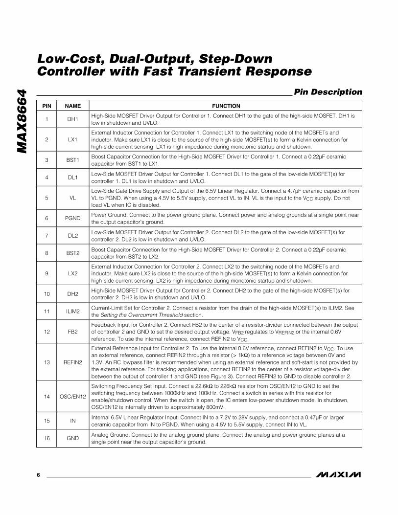
Figure 5. 300kHz Circuit with 7.2V to 20V Input

MA
X8
66
4
Low-Cost, Dual-Output, Step-DownController with Fast Transient Response
18 ______________________________________________________________________________________
Power-Up and SequencingThe MAX8664 features an OSC/EN12 input that is usedboth for setting the switching frequency and as anenable input for both controllers. A resistor fromOSC/EN12 to GND sets the switching frequency, andwhen OSC/EN12 is high impedance, both controllersenter low-power shutdown mode. This is easilyachieved with a transistor between the resistor andGND. Figure 6a shows the startup configuration withindependent outputs. With REFIN2 connected to VCC,both controllers use the internal reference.
For tracking applications, connect REFIN2 to the centerof a resistive voltage-divider between the output of con-troller 1 and GND. See Figure 6b. In this application,the output of regulator 2 tracks the output voltage ofcontroller 1. The voltage-divider resistors set theVOUT2/VOUT1 ratio. A typical tracking application is forthe VTT supply of DDR memory.
Figure 6c shows one method of sequencing the out-puts. Output 1 rises first. When PWRGD goes high, thetransistors allow the external reference to drive REFIN2and output 2 rises. The circuit in Figure 6d functionssimilarly, except the enable signal is supplied externallyinstead of being driven by the PWRGD signal.
Table 5. Component List for Figure 5DESIGNATION QTY DESCRIPTION
C1, C13 20.01µF, 10V X7R ceramiccapacitors
C2, C3, C14, C15 4 10µF, 25V X5R ceramic capacitors
C5 1 1µF, 25V X5R ceramic capacitor
C6 1 1µF, 10V X5R ceramic capacitor
C7, C16 20.22µF, 10V X7R ceramiccapacitors
C8, C17 24700pF, 10V X7R ceramiccapacitors
C9, C18 2470µF/2.5V POSCAP capacitorsSanyo 2R5TPD470M6
C10, C19 2 10µF, 6.3V X5R ceramic capacitors
C11, C20 21000pF, 25V X7R ceramiccapacitors
C12 1 4.7µF, 10V X5R ceramic capacitor
DESIGNATION QTY DESCRIPTION
L1, L2 21.43µH, 4.52mΩ inductorsPanasonic ETQP3H1E4BFA
N1–N4 4n-channel MOSFETsIRF7821 (8-pin SOs)
N5 1n-channel MOSFET2N7002 (SOT23)
R1 1 2.87kΩ ±1% resistor (0402 or 0603)
R2 1 40.2kΩ ±1% resistor (0402 or 0603)
R3, R11 2 10kΩ ±1% resistors (0402 or 0603)
R4 1 5.36kΩ ±1% resistor (0402 or 0603)
R5, R10 2 2.0Ω ±5% resistors (1206)
R6 1 2.26kΩ ±1% resistor (0402 or 0603)
R7 1 10kΩ ±5% resistor (0402 or 0603)
R8 1 75kΩ ±1% resistor (0402 or 0603)
R9 1 25.5kΩ ±1% resistor (0402 or 0603)
R12 1 9.53kΩ ±1% resistor (0402 or 0603)
VCC
REFIN2
OSC/EN12ONOFF
CHIPENABLE
CHIPENABLE
PWRGD
VOUT2
VOUT1
MAX8664
Figure 6a. Two Independent Output Startup and Shutdown Waveforms

MA
X8
66
4
Low-Cost, Dual-Output, Step-DownController with Fast Transient Response
______________________________________________________________________________________ 19
REFIN2
OSC/EN12
VOUT1
ONOFF
CHIPENABLE
CHIPENABLE
PWRGD
VOUT2
VOUT1
MAX8664
Figure 6b. Ratiometric Tracking Startup and Shutdown Waveforms
REFIN2
OSC/EN12
EXTERNALREF
VCC
ONOFF
CHIPENABLE
CHIPENABLE
PWRGD
PWRGD
VOUT2
VOUT1
MAX8664
Figure 6c. Sequencing Startup and Shutdown Waveforms

MA
X8
66
4
Low-Cost, Dual-Output, Step-DownController with Fast Transient Response
20 ______________________________________________________________________________________
Design ProcedureSetting the Switching Frequency
Connect a resistor from OSC/EN12 to GND to set theswitching frequency between 100kHz and 1000kHz.Calculate the resistor value (R10 in Figures 2–5) as follows:
Inductor SelectionThere are several parameters that must be examinedwhen determining which inductor is to be used. Inputvoltage, output voltage, load current, switching fre-quency, and LIR. LIR is the ratio of inductor-current rip-ple to maximum DC load current (ILOAD(MAX)). A higherLIR value allows for a smaller inductor, but results inhigher losses and higher output ripple. A good compro-mise between size and efficiency is an LIR of 0.3. Onceall the parameters are chosen, the inductor value isdetermined as follows:
where fS is the switching frequency. Choose a standardvalue inductor close to the calculated value. The exact
inductor value is not critical and can be adjusted to maketrade-offs among size, cost, and efficiency. Lower induc-tor values minimize size and cost, but they also increasethe output ripple and reduce the efficiency due to higherpeak currents. On the other hand, higher inductor valuesincrease efficiency, but eventually resistive losses due toextra turns of wire exceed the benefit gained from lowerAC current levels. This is especially true if the inductanceis increased without also increasing the physical size ofthe inductor. Find a low-loss inductor having the lowestpossible DC resistance that fits the allotted dimensions.The chosen inductor’s saturation current rating mustexceed the peak inductor current determined as:
Output CapacitorThe key selection parameters for the output capacitorare the actual capacitance value, the equivalent seriesresistance (ESR), the equivalent series inductance(ESL), and the voltage-rating requirements. Theseparameters affect the overall stability, output voltageripple, and transient response. The output ripple hasthree components: variations in the charge stored inthe output capacitor, the voltage drop across thecapacitor’s ESR, and ESL caused by the current intoand out of the capacitor. The maximum output voltageripple is estimated as follows:
I ILIR
IPEAK LOAD MAX LOAD MAX= + ×( ) ( )2
LV V V
V f I LIROUT IN OUT
IN S LOAD MAX=
× −
× × ×
( )
( )
RHz
fS10
2 24 1010=
×. ( )( )Ω
REFIN2
OSC/EN12
CHIPENABLE
OUT2ENABLE
OUT2ENABLE
PWRGD
VOUT2
VOUT1
MAX8664
ONOFF
ONOFF
CHIPENABLE
EXTERNALREFVCC
Figure 6d. Sequencing Startup and Shutdown Waveforms with System Enable 2 Signal

MA
X8
66
4
Low-Cost, Dual-Output, Step-DownController with Fast Transient Response
______________________________________________________________________________________ 21
VRIPPLE = VRIPPLE(ESR) + VRIPPLE(C) + VRIPPLE(ESL)
The output voltage ripple as a consequence of theESR, ESL, and output capacitance is:
where IP-P is the peak-to-peak inductor current:
These equations are suitable for initial capacitor selec-tion, but final values should be chosen based on a pro-totype or evaluation circuit. As a general rule, a smallerripple current results in less output-voltage ripple. Sincethe inductor ripple current is a factor of the inductorvalue and input voltage, the output-voltage rippledecreases with larger inductance, and increases withhigher input voltages. Ceramic, tantalum, or aluminumpolymer electrolytic capacitors are recommended. Thealuminum electrolytic capacitor is the least expensive;however, it has higher ESR and ESL. To compensate forthis, use a ceramic capacitor in parallel to reduce theswitching ripple and noise. For reliable and safe opera-tion, ensure that the capacitor’s voltage and ripple-cur-rent ratings exceed the calculated values.
The response to a load transient depends on theselected output capacitors. After a load transient, the
output voltage instantly changes by ESR x ΔILOAD.Before the controller can respond, the output voltagedeviates further depending on the inductor and outputcapacitor values. After a short period of time (see theTypical Operating Characteristics), the controllerresponds by regulating the output voltage back to itsnominal state. The controller response time depends onits closed-loop bandwidth. With a higher bandwidth,the response time is faster, thus preventing the outputvoltage from further deviation from its regulating value.
Setting the Output Voltages and VoltagePositioning
Figure 7 shows the feedback network used on theMAX8664. With this configuration, a portion of the feed-back signal is sensed on the switched side of theinductor (LX), and the output voltage droops slightly asthe load current is increased due to the DC resistanceof the inductor (DCR). This allows the load regulation tobe set to match the voltage droop during a load tran-sient (voltage positioning), reducing the peak-to-peakoutput voltage deviation during a load transient, andreducing the output capacitance requirements.
To set the magnitude of the voltage positioning, selecta value for R2 in the 8kΩ to 24kΩ range, then calculatethe value of R1 as follows:
where IOUT(MAX) is the maximum output current andΔ VOUT(MAX) is the maximum allowable droop in theoutput voltage at full load.
R RI DCR
VOUT MAX
OUT MAX1 2 1= ×
×−
⎛
⎝⎜
⎞
⎠⎟
( )
( )Δ
IV V
f LVV
P PIN OUT
S
OUT
IN− =
−
××
V I ESR
VV
L ESLESL
VI
C f
RIPPLE ESR P P
RIPPLE ESLIN
RIPPLE CP P
OUT S
( )
( )
( )
= ×
=+
×
=× ×
−
−
8
L DCRLX_
FB_
OUT
ESR
COUT
RLOADR1
R2
R3
Cr
Figure 7. Feedback Network

MA
X8
66
4
Low-Cost, Dual-Output, Step-DownController with Fast Transient Response
22 ______________________________________________________________________________________
To set the no-load output voltage (VOUT), calculate thevalue of R3 as follows:
where VFB is the feedback regulation voltage (0.6Vwhen using the internal reference or VREFIN2 for exter-nal reference). If the desired output voltage is equal tothe reference voltage (typical for tracking applications),R3 is not installed.
To achieve the lowest possible load regulation in appli-cations where voltage positioning is not desired, R1 isnot installed and R3 is calculated as follows:
CompensationTo ensure stable operation, connect a compensationcapacitor (Cr) across the upper feedback resistor asshown in Figure 7. To find the value of this capacitor,follow the compensation design procedure below.
Choose a closed-loop bandwidth (fC) that is less than1/3 the switching frequency (fS). Calculate the outputdouble pole (fO) as follows:
The FB peak-to-peak voltage ripple is:
The output ripple voltage due to the ESR of the outputcapacitor, COUT, is:
Target the feedback ripple in the 25mV to 60mV range.For high duty-cycle applications (> 70%), a feedbackripple of 25mV is recommended.
Finally, calculate the value of Cr as follows:
MOSFET SelectionEach output of the MAX8664 is capable of driving two tofour external, logic-level, n-channel MOSFETs as the cir-cuit switch elements. The key selection parameters are:
• On-resistance (RDS(ON))—the lower, the better.
• Maximum Drain-to-Source Voltage (VDSS)—shouldbe at least 20% higher than the input supply rail atthe high-side MOSFET’s drain.
• Gate charges (Qg, Qgd, Qgs)— the lower, the better.
For a 5V input application, choose MOSFETs with ratedRDS(ON) at VGS ≤ 4.5V. With higher input voltages, theinternal VL regulator provides 6.5V for gate drive inorder to minimize the on-resistance for a wide range ofMOSFETs.
For a good compromise between efficiency and cost,choose the high-side MOSFETs that have conductionlosses equal to switching losses at nominal input voltageand output current. Low RDS(ON) is preferred for low-side MOSFETs. Make sure that the low-side MOSFET(s)does not spuriously turn on due to dV/dt caused by thehigh-side MOSFET(s) turning on, as this would result inshoot-through current and degrade the efficiency.MOSFETs with a lower Qgd / Qgs ratio have higherimmunity to dV/dt. For high-current applications, it isoften preferable to parallel two MOSFETs rather than touse a single large MOSFET.
For proper thermal management, the power dissipationmust be calculated at the desired maximum operatingjunction temperature, maximum output current, andworst-case input voltage. For the-low side MOSFET(s),the worst-case power dissipation occurs at the highestduty cycle (VIN(MAX)). The low-side MOSFET(s) operateas zero voltage switches; therefore, major losses arethe channel conduction loss (PLSCC) and the bodydiode conduction loss (PLSDC):
Use RDS(ON) at TJ(MAX):
PLSDC(MAX) = 2 x ILOAD(MAX) VF x tDT x fSwhere VF is the body diode forward-voltage drop, tDT is thedead time between high-side and low-side switching tran-sitions (25ns typical), and fS is the switching frequency.
P
LSCC MAXOUT
IN MAX LOAD MAX DS ONV
VI R( )
( ) ( ) ( )= −⎛
⎝⎜
⎞
⎠⎟ × ×1 2
Cr
VV
V V
R f V V
OUT
ININ OUT
S FB RIPPLE OUT RIPPLE=
−( )× × −( )1 | |_ _
V
VV
V V
L f
ESRC f
OUT RIPPLE
OUT
ININ OUT
S
O S
_
=−( )
××
+× ×
⎛⎝⎜
⎞⎠⎟
18
V
RR
RR
RR
VDCR
Rff
FB RIPPLEOUT
LOAD
C
O
_ =+
+ +
⎛
⎝
⎜⎜⎜
⎞
⎠
⎟⎟⎟
×
+⎛⎝⎜
⎞⎠⎟ ×
⎛
⎝
⎜⎜⎜⎜
⎞
⎠
⎟⎟⎟⎟
121
123
21
1
f
L CR ESRR DCR
O
OUTLOAD
LOAD
=
× ×++
1
2π
RV
V VRFB
OUT FB3 2=
−
⎛⎝⎜
⎞⎠⎟ ×
RV
V VR RR R
FB
OUT FB3
1 21 2
=−
⎛
⎝⎜
⎞
⎠⎟
×
+⎛⎝⎜
⎞⎠⎟

MA
X8
66
4
Low-Cost, Dual-Output, Step-DownController with Fast Transient Response
______________________________________________________________________________________ 23
The high-side MOSFET(s) operate as duty-cycle controlswitches and have the following major losses: the chan-nel conduction loss (PHSCC), the overlapping switchingloss (PHSSW), and the drive loss (PHSDR). The maxi-mum power dissipation could occur either at VIN(MAX)or VIN(MIN):
Use RDS(ON) at TJ(MAX):
where IGATE is the average DH driver output-currentcapability determined by:
where RDS(ON)(DR) is the DH_ driver’s on-resistance(see the Electrical Characteristics) and RGATE is theinternal gate resistance of the MOSFET (~ 2Ω):
where VGS ≈ VVL.
The high-side MOSFET(s) do not have body diode con-duction loss, unless the converter is sinking current.When sinking current, calculate this loss asPHSDC(MAX) = ILOAD(MAX) x VF x (2 x tDT + tWD) x fS,where tWD is about 130ns.
Allow an additional 20% for losses due to MOSFET out-put capacitances and low-side MOSFET body diodereverse-recovery charge dissipated in the high-sideMOSFET(s). Refer to the MOSFET data sheet for ther-mal resistance specifications to calculate the PCB areaneeded to maintain the desired maximum operatingjunction temperature with the above calculated powerdissipations.
MOSFET Snubber CircuitFast switching transitions cause ringing because of res-onating circuit parasitic inductance and capacitance atthe switching nodes. This high-frequency ringingoccurs at LX’s rising and falling transitions and can
interfere with circuit performance and generate EMI. Todampen this ringing, a series RC snubber circuit isadded across each low-side switch. Below is the pro-cedure for selecting the value of the series RC circuit.
Connect a scope probe to measure VLX_ to GND andobserve the ringing frequency, fR.
Find the capacitor value (connected from LX_ to GND)that reduces the ringing frequency by half.
The circuit parasitic capacitance (CPAR) at LX_ is thenequal to 1/3 the value of the added capacitance above.The circuit parasitic inductance (LPAR) is calculated by:
The resistor for critical dampening (RSNUB) is equal to2π x fR x LPAR. Adjust the resistor value up or down totailor the desired damping and the peak-voltage excur-sion.
The capacitor (CSNUB) should be at least 2 to 4 timesthe value of the CPAR to be effective. The power loss ofthe snubber circuit is dissipated in the resistor(PRSNUB) and can be calculated as:
where VIN is the input voltage and fSW is the switchingfrequency. Choose an RSNUB power rating that meetsthe specific application’s derating rule for the powerdissipation calculated.
Setting the Overcurrent ThresholdConnect a resistor from ILIM_ to the drain of the high-side MOSFET(s) to set the overcurrent protectionthreshold. ILIM_ sinks 50µA (typ) through this resistor.When the drain-source voltage exceeds the voltagedrop across this resistor during the high-side MOS-FET(s) on-time, overcurrent protection is triggered. Toset the output current level where overcurrent protec-tion is triggered (ILIMIT), calculate the value of the ILIM_resistor as follows:
where RDS(ON)HS is the maximum on-resistance of thehigh-side MOSFET(s) at +25°C. At higher tempera-tures, the ILIM current increases to compensate for thetemperature coefficient of the high-side MOSFET(s).
RR I
AILIM
DS ON HS LIMIT _
( )=×
50μ
P C V fRSNUB SNUB IN SW = × ( ) ×2
Lf C
PARR PAR
=( ) ×
1
2 2π
P Q V fR
R RHSDR G GS S
GATE
GATE DS ON DR = × × ×
+ ( )( )
IV
R RGATE
VL
DS ON DR GATE≅
×
+
0 5.
( )( )
P V IQI
fHSSW MAX IN MAX LOAD MAXGD
GATES ( ) ( ) ( )= × × ×
PV
VI RHSCC MAX
OUT
IN MIN LOAD MAX DS ON
( )( ) ( ) ( )= × ×2

MA
X8
66
4
Low-Cost, Dual-Output, Step-DownController with Fast Transient Response
24 ______________________________________________________________________________________
Input CapacitorThe input filter capacitors reduce peak currents drawnfrom the power source and reduce noise and voltageripple on the input caused by the circuit’s switching.The input capacitors must meet the ripple currentrequirement (IRMS) imposed by the switching currents.The ripple current requirement can be estimated by thefollowing equation:
Choose a capacitor that exhibits less than 10°C tem-perature rise at the maximum operating RMS current foroptimum long-term reliability.
Applications InformationPCB Layout Guidelines
Careful PCB layout is an important factor in achievinglow switching losses and clean, stable operation. Theswitching power stage requires particular attention.Follow these guidelines for good PCB layout:
1) A multilayer PCB is recommended.
2) Place IC decoupling capacitors as close as possi-ble to the IC pins. Keep separate power groundand signal ground planes. Place the low-sideMOSFETs near the PGND pin. Arrange the high-side MOSFETs and low-side MOSFETs in such a
way that the high-side MOSFET’s drain is close andnear the low-side MOSFET’s source. This allows theinput ceramic decoupling capacitor to be placeddirectly across and as close as possible to thehigh-MOSFET’s drain and the low-side MOSFET’ssource. This helps contain the high switching cur-rent within this small loop.
3) Pour an analog ground plane in the second layerunderneath the IC to minimize noise coupling.
4) Connect input, output, and VL capacitors to thepower ground plane; connect all other capacitors tothe signal ground plane.
5) Place the MOSFETs as close as possible to the ICto minimize trace inductance of the gate drive loop.If parallel MOSFETs are used, keep the tracelengths to both gates equal and short.
6) Connect the drain leads of the power MOSFET to alarge copper area to help cool the device. Refer tothe power MOSFET data sheet for recommendedcopper area.
7) Place the feedback network components as closeas possible to the IC pins.
8) The current-limit setting RC should be Kelvin con-nected to the high-side MOSFETs’ drain.
Refer to the MAX8664 evaluation kit for an example layout.
IV
I V V V I V V VRMSIN
OUT OUT IN OUT OUT OUT IN OUT= ( ) × × −( ) + ( ) × × −( )11
21 1 2
22 2

MA
X8
66
4
Low-Cost, Dual-Output, Step-DownController with Fast Transient Response
______________________________________________________________________________________ 25
Chip InformationPROCESS: BiCMOS
20
19
18
17
16
15
14
13
1
2
3
4
5
6
7
8
DH1 ILIM1
FB1
PWRGD
VCC
GND
IN
OSC/EN12
REFIN2
TOP VIEW
MAX8664
QSOP
LX1
BST1
PGND
DL1
VL
DL2
BST2
12
11
9
10
FB2
ILIM2
LX2
DH2
Pin Configuration
MA
X8
66
4
Low-Cost, Dual-Output, Step-DownController with Fast Transient Response
Maxim cannot assume responsibility for use of any circuitry other than circuitry entirely embodied in a Maxim product. No circuit patent licenses areimplied. Maxim reserves the right to change the circuitry and specifications without notice at any time.
26 ____________________Maxim Integrated Products, 120 San Gabriel Drive, Sunnyvale, CA 94086 408-737-7600
© 2007 Maxim Integrated Products is a registered trademark of Maxim Integrated Products, Inc.
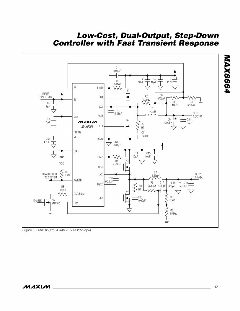
Package Information(The package drawing(s) in this data sheet may not reflect the most current specifications. For the latest package outline informationgo to www.maxim-ic.com/packages.)
QS
OP
.EP
S