Embed Size (px)
Citation preview
Low-Cost and Area-Efficient FPGA Implementations
of Lattice-Based Cryptography
Aydin Aysu, Cameron Patterson and Patrick Schaumont
Electrical and Computer Engineering Department
Virginia Tech
Blacksburg, VA, USA
e-mail: { aydinay,cdp,schaum }@vt.edu
Abstract— The interest in lattice-based cryptography is increasing
due to its quantum resistance and its provable security under
some worst-case hardness assumptions. As this is a relatively new
topic, the search for efficient hardware architectures for lattice-
based cryptographic building blocks is still an active area of
research. We present area optimizations for the most critical and
computationally-intensive operation in lattice-based
cryptography: polynomial multiplication with the Number
Theoretic Transform (NTT). The proposed methods are
implemented on an FPGA for polynomial multiplication over the
ideal [ ]⟨ ⟩. The proposed hardware architectures reduce
slice usage, number of utilized memory blocks and total memory
accesses by using a simplified address generation, improved
memory organization and on-the-fly operand generations.
Compared to prior work, with similar performance the proposed
hardware architectures can save up to 67% of occupied slices,
80% of used memory blocks and 60% of memory accesses, and
can fit into smallest Xilinx Spartan-6 FPGA.
Keywords— Lattice-based cryptography; Number Theoretic
Transform; FPGA; ideal lattices
I. INTRODUCTION
Lattice-based cryptography relies on the hardness of lattice
problems. Lattice-based cryptosystems are quantum resistant
and are often provably secure based on worst-case hardness
assumptions. In recent years, this resulted in development of
several cryptographic primitives such as digital signatures [1],
encryption schemes [2] and fully homomorphic encryption [3].
An excellent tutorial on lattice theory and associated hardness
problems can be found in [4].
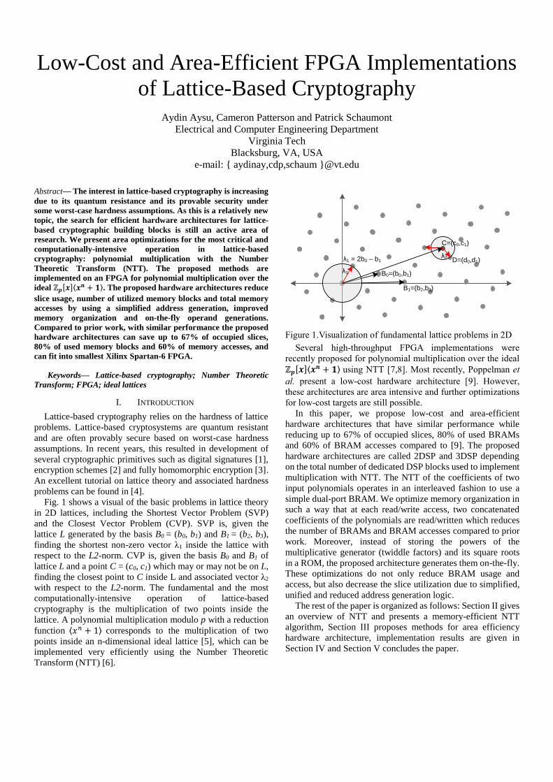
Fig. 1 shows a visual of the basic problems in lattice theory
in 2D lattices, including the Shortest Vector Problem (SVP)
and the Closest Vector Problem (CVP). SVP is, given the
lattice L generated by the basis B0 = (b0, b1) and B1 = (b2, b3),
finding the shortest non-zero vector λ1 inside the lattice with
respect to the L2-norm. CVP is, given the basis B0 and B1 of
lattice L and a point C = (c0, c1) which may or may not be on L,
finding the closest point to C inside L and associated vector λ2
with respect to the L2-norm. The fundamental and the most
computationally-intensive operation of lattice-based
cryptography is the multiplication of two points inside the
lattice. A polynomial multiplication modulo p with a reduction
function ⟨ ⟩ corresponds to the multiplication of two
points inside an n-dimensional ideal lattice [5], which can be
implemented very efficiently using the Number Theoretic
Transform (NTT) [6].
Figure 1.Visualization of fundamental lattice problems in 2D
Several high-throughput FPGA implementations were
recently proposed for polynomial multiplication over the ideal
[ ]⟨ ⟩ using NTT [7,8]. Most recently, Poppelman et
al. present a low-cost hardware architecture [9]. However,
these architectures are area intensive and further optimizations
for low-cost targets are still possible.
In this paper, we propose low-cost and area-efficient
hardware architectures that have similar performance while
reducing up to 67% of occupied slices, 80% of used BRAMs
and 60% of BRAM accesses compared to [9]. The proposed
hardware architectures are called 2DSP and 3DSP depending
on the total number of dedicated DSP blocks used to implement
multiplication with NTT. The NTT of the coefficients of two
input polynomials operates in an interleaved fashion to use a
simple dual-port BRAM. We optimize memory organization in
such a way that at each read/write access, two concatenated
coefficients of the polynomials are read/written which reduces
the number of BRAMs and BRAM accesses compared to prior
work. Moreover, instead of storing the powers of the
multiplicative generator (twiddle factors) and its square roots
in a ROM, the proposed architecture generates them on-the-fly.
These optimizations do not only reduce BRAM usage and
access, but also decrease the slice utilization due to simplified,
unified and reduced address generation logic.
The rest of the paper is organized as follows: Section II gives
an overview of NTT and presents a memory-efficient NTT
algorithm, Section III proposes methods for area efficiency
hardware architecture, implementation results are given in
Section IV and Section V concludes the paper.
λ1 = 2b0 – b1
λ1
λ2
B0=(b0,b1)
B1=(b2,b3)
C=(c0,c1)
D=(d0,d1)
II. NUMBER THEORETIC TRANSFORM
A. Overview
NTT is essentially a Discrete Fourier Transform defined over a finite field or ring and does not require complex arithmetic [10]. The generic forward NTTn(a) transforms a n-1 degree polynomial of the form
( )
( )
with the modulo p coefficients (a0, a1, … , an-1) into a n-1 degree polynomial of the form
( )
( )
with the modulo p coefficients (A0,A1,…,An-1) defined as
∑
( )
with (twiddle factor) a given primitive n-th root over the polynomial ring. The inverse transform,
, computes:
∑
( )
The NTT exists if and only if for some integer k, p = kn + 1, ωn
= 1 (mod p), and .
The complexity of schoolbook polynomial multiplication is O(n2) which makes it unfeasible to use for large n values (a typical n value for lattice-based cryptography is 1024). NTT reduces the cost of multiplication to a quasi-linear complexity of n(log n). The multiplication of two (n-1)-degree polynomials can be calculated using Equation (5);
( ( ) ( )) ( )
where “.” represents point-wise multiplication.
If the Equation (5) is used for multiplication, prior to NTT the coefficients of the input polynomials should be doubled (2n) by zero-padding. Moreover, if the multiplication is done over a polynomial field of the form [ ]⟨𝒇( )⟩ the resulting
polynomial of the multiplication with 2n coefficients should be reduced back into a polynomial with n coefficients (n-1 degree) with respect to the reduction function f(x).
When the reduction function is ⟨ ⟩ , NTT is referred to as a Fermat Theoretic Transform (FTT). In this case a special mathematical property increases the efficiency of using FTT further [10]. Equation (6) shows the case of FTT.
( ( ) ( )) ( )
where and
(
)
(
)
(
) (7)
When the reduction function is ⟨ ⟩ the NTT operations can be directly applied to a polynomial with n coefficients without zero-padding to a polynomial of 2n coefficients. However in this case the coefficients of the polynomial should
be multiplied by powers of prior to NTT and the resulting vector should be multiplied by the powers of to convert back to c. While these operations add 2n multiplications, the NTT size is halved and the reduction operation is eliminated.
B. Memory-Efficient NTT Algorithm
Pseudo-code for the NTT is given in Listing 1 [11]. There are log n stages, and at each stage a total of n values are evaluated. At each iteration of the inner loop two values are generated as in a Cooley-Tukey (CT) radix-2 butterfly [12], hence it takes (n/2)(log n) iterations to complete the NTT operation of a polynomial with n coefficients. The algorithm in Listing 1 is memory-efficient compared to the algorithm used in [9] since the value is generated inside the inner-loop (line 13).
𝑰 𝒖𝒕 ∶ 𝑢𝑙𝑢𝑠 ( ) 𝑠 𝑧𝑒 𝑡ℎ𝑒 𝑡𝑟 𝑠 𝑟 𝑡 (
𝑘 𝑘 ⋲ ℕ) 𝑟 𝑡 𝑣𝑒 𝑟 𝑡 𝑢 𝑡𝑦 𝑒𝑔𝑟𝑒𝑒 ( ⋲ 𝑝)
𝑒 𝑒 𝑡𝑠 𝑙𝑦 𝑙 𝑒𝑔𝑟𝑒𝑒 ( ⋲ 𝑝[ ])
𝑶𝒖𝒕 𝒖𝒕 ∶ ( ⋲ 𝑝[ ])
𝑡𝑟𝑒𝑣𝑒𝑟𝑠𝑒( )
𝒇𝒐𝒓 𝑡 𝑙 𝑔 ( ) 𝑡𝑒 _ 𝑙_ 𝒇𝒐𝒓 𝑗 𝑡 𝒇𝒐𝒓 𝑡 𝑡 ( / + ) 7 𝑒 _ ((𝑡) + ) 𝑗 8 𝑒 _ 𝑒 _ 9 ( 𝑒 _ ); ( 𝑒 _ ); 𝐶 _𝑂𝑢𝑡_ ( 𝑙_ ) % 𝐶 _𝑂𝑢𝑡_ ( 𝑙_ )% ( 𝑒 _ ) 𝐶 _𝑂𝑢𝑡_ ( 𝑒 _ ) 𝐶 _𝑂𝑢𝑡_ 𝑡𝑒 _ (𝑡𝑒 _ ) % 𝒆 𝒅 7 𝑙_ 𝑡𝑒 _ 8 𝒆 𝒅 9 𝒆 𝒅 Listing 1: Pseudo-code of memory-efficient NTT algorithm
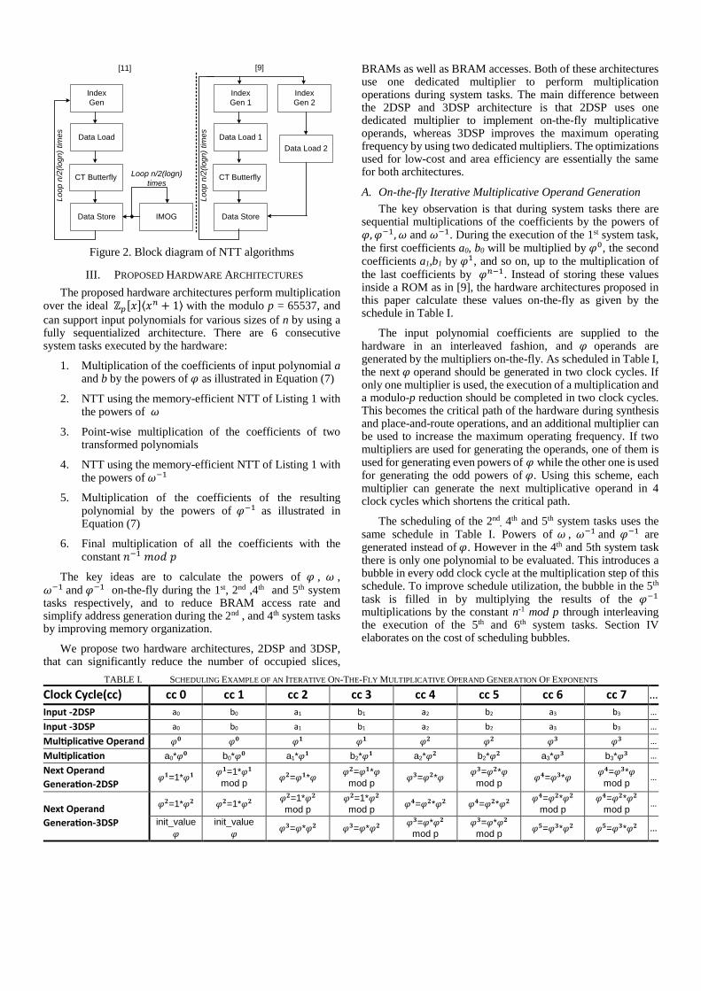
Fig. 2 shows the high-level block diagram of the memory-efficient NTT algorithm and the algorithm used in [9]. Index
generation (Index Gen) calculates the index values for each
iteration. Data Load uses the calculated index values to generate required data. Iterative Multiplicative Operand
Generator (IMOG) produces the 𝑙_ values. CT
Butterfly executes the CT radix-2 butterfly and Data
Store stores the results of each iteration. The algorithm in
Listing 1 uses IMOG to produce 𝑙_ values whereas an
additional Index Gen and Data Load is used in [9].
After the NTT of two vectors are calculated, point-wise multiplication and the inverse NTT should also be computed. In the case of FTT, additional operations such as multiplication by the powers of and as defined in Equation (7) should also be computed.
} ButterflyCT
} genindex
} loaddata
} IMOG
} storedata
Index
Gen
Data Load
CT Butterfly
IMOG
Index
Gen 2
[11] [9]
Data Load 2
Data Store
Lo
op
n/2
(lo
gn
) tim
es
Index
Gen 1
Data Load 1
CT Butterfly
Data Store
Lo
op
n/2
(lo
gn
) tim
es
Loop n/2(logn)
times
Figure 2. Block diagram of NTT algorithms
III. PROPOSED HARDWARE ARCHITECTURES
The proposed hardware architectures perform multiplication over the ideal 𝑝[ ]⟨
⟩ with the modulo p = 65537, and
can support input polynomials for various sizes of n by using a fully sequentialized architecture. There are 6 consecutive system tasks executed by the hardware:
1. Multiplication of the coefficients of input polynomial a and b by the powers of as illustrated in Equation (7)
2. NTT using the memory-efficient NTT of Listing 1 with the powers of
3. Point-wise multiplication of the coefficients of two transformed polynomials
4. NTT using the memory-efficient NTT of Listing 1 with the powers of
5. Multiplication of the coefficients of the resulting polynomial by the powers of as illustrated in Equation (7)
6. Final multiplication of all the coefficients with the constant
The key ideas are to calculate the powers of , , and on-the-fly during the 1st, 2nd ,4th and 5th system tasks respectively, and to reduce BRAM access rate and simplify address generation during the 2nd , and 4th system tasks by improving memory organization.
We propose two hardware architectures, 2DSP and 3DSP, that can significantly reduce the number of occupied slices,
BRAMs as well as BRAM accesses. Both of these architectures use one dedicated multiplier to perform multiplication operations during system tasks. The main difference between the 2DSP and 3DSP architecture is that 2DSP uses one dedicated multiplier to implement on-the-fly multiplicative operands, whereas 3DSP improves the maximum operating frequency by using two dedicated multipliers. The optimizations used for low-cost and area efficiency are essentially the same for both architectures.
A. On-the-fly Iterative Multiplicative Operand Generation
The key observation is that during system tasks there are sequential multiplications of the coefficients by the powers of and . During the execution of the 1st system task, the first coefficients a0, b0 will be multiplied by , the second coefficients a1,b1 by , and so on, up to the multiplication of the last coefficients by . Instead of storing these values inside a ROM as in [9], the hardware architectures proposed in this paper calculate these values on-the-fly as given by the schedule in Table I.
The input polynomial coefficients are supplied to the hardware in an interleaved fashion, and operands are generated by the multipliers on-the-fly. As scheduled in Table I, the next operand should be generated in two clock cycles. If only one multiplier is used, the execution of a multiplication and a modulo-p reduction should be completed in two clock cycles. This becomes the critical path of the hardware during synthesis and place-and-route operations, and an additional multiplier can be used to increase the maximum operating frequency. If two multipliers are used for generating the operands, one of them is used for generating even powers of while the other one is used for generating the odd powers of . Using this scheme, each multiplier can generate the next multiplicative operand in 4 clock cycles which shortens the critical path.
The scheduling of the 2nd, 4th and 5th system tasks uses the
same schedule in Table I. Powers of , and are generated instead of . However in the 4th and 5th system task there is only one polynomial to be evaluated. This introduces a bubble in every odd clock cycle at the multiplication step of this schedule. To improve schedule utilization, the bubble in the 5th task is filled in by multiplying the results of the multiplications by the constant n-1 mod p through interleaving the execution of the 5th and 6th system tasks. Section IV elaborates on the cost of scheduling bubbles.
TABLE I. SCHEDULING EXAMPLE OF AN ITERATIVE ON-THE-FLY MULTIPLICATIVE OPERAND GENERATION OF EXPONENTS
Clock Cycle(cc) cc 0 cc 1 cc 2 cc 3 cc 4 cc 5 cc 6 cc 7 …
Input -2DSP a0 b0 a1 b1 a2 b2 a3 b3 …
Input -3DSP a0 b0 a1 b1 a2 b2 a3 b3 …
Multiplicative Operand 𝟎 𝟎 𝟐 𝟐 𝟑 𝟑 …
Multiplication a0* 𝟎 b0* 𝟎 a1* b2* a2* 𝟐 b2* 𝟐 a3* 𝟑 b3* 𝟑 …
Next Operand
Generation-2DSP =1*
=1* mod p
𝟐= * 𝟐= *
mod p 𝟑= 𝟐*
𝟑= 𝟐*
mod p 𝟒= 𝟑*
𝟒= 𝟑*
mod p …
Next Operand
Generation-3DSP
𝟐=1* 𝟐 𝟐=1* 𝟐 𝟐=1* 𝟐 mod p
𝟐=1* 𝟐 mod p
𝟒= 𝟐* 𝟐 𝟒= 𝟐* 𝟐 𝟒= 𝟐* 𝟐
mod p 𝟒= 𝟐* 𝟐
mod p …
init_value
init_value
𝟑= * 𝟐 𝟑= * 𝟐
𝟑= * 𝟐 mod p
𝟑= * 𝟐 mod p
𝟓= 𝟑* 𝟐 𝟓= 𝟑* 𝟐 …
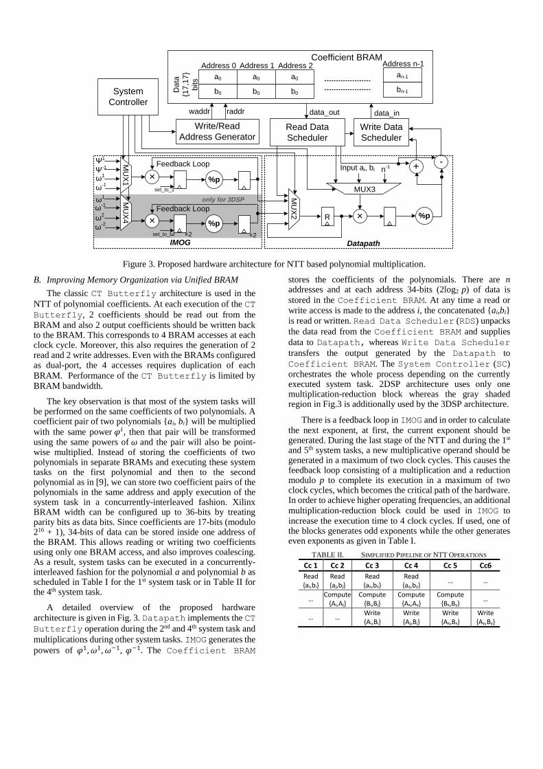
Figure 3. Proposed hardware architecture for NTT based polynomial multiplication.
B. Improving Memory Organization via Unified BRAM
The classic CT Butterfly architecture is used in the
NTT of polynomial coefficients. At each execution of the CT
Butterfly, 2 coefficients should be read out from the BRAM and also 2 output coefficients should be written back to the BRAM. This corresponds to 4 BRAM accesses at each clock cycle. Moreover, this also requires the generation of 2 read and 2 write addresses. Even with the BRAMs configured as dual-port, the 4 accesses requires duplication of each
BRAM. Performance of the CT Butterfly is limited by BRAM bandwidth.
The key observation is that most of the system tasks will be performed on the same coefficients of two polynomials. A coefficient pair of two polynomials {ai, bi} will be multiplied
with the same power , then that pair will be transformed using the same powers of and the pair will also be point-wise multiplied. Instead of storing the coefficients of two polynomials in separate BRAMs and executing these system tasks on the first polynomial and then to the second polynomial as in [9], we can store two coefficient pairs of the polynomials in the same address and apply execution of the system task in a concurrently-interleaved fashion. Xilinx BRAM width can be configured up to 36-bits by treating parity bits as data bits. Since coefficients are 17-bits (modulo 216 + 1), 34-bits of data can be stored inside one address of the BRAM. This allows reading or writing two coefficients using only one BRAM access, and also improves coalescing. As a result, system tasks can be executed in a concurrently-interleaved fashion for the polynomial a and polynomial b as scheduled in Table I for the 1st system task or in Table II for the 4th system task.
A detailed overview of the proposed hardware
architecture is given in Fig. 3. Datapath implements the CT
Butterfly operation during the 2nd and 4th system task and
multiplications during other system tasks. IMOG generates the
powers of The Coefficient BRAM
stores the coefficients of the polynomials. There are n addresses and at each address 34-bits (2log2 p) of data is
stored in the Coefficient BRAM. At any time a read or write access is made to the address i, the concatenated {ai,bi}
is read or written. Read Data Scheduler (RDS) unpacks
the data read from the Coefficient BRAM and supplies
data to Datapath, whereas Write Data Scheduler
transfers the output generated by the Datapath to
Coefficient BRAM. The System Controller (SC) orchestrates the whole process depending on the currently executed system task. 2DSP architecture uses only one multiplication-reduction block whereas the gray shaded region in Fig.3 is additionally used by the 3DSP architecture.
There is a feedback loop in IMOG and in order to calculate the next exponent, at first, the current exponent should be generated. During the last stage of the NTT and during the 1st and 5th system tasks, a new multiplicative operand should be generated in a maximum of two clock cycles. This causes the feedback loop consisting of a multiplication and a reduction modulo p to complete its execution in a maximum of two clock cycles, which becomes the critical path of the hardware. In order to achieve higher operating frequencies, an additional
multiplication-reduction block could be used in IMOG to increase the execution time to 4 clock cycles. If used, one of the blocks generates odd exponents while the other generates even exponents as given in Table I.
TABLE II. SIMPLIFIED PIPELINE OF NTT OPERATIONS
Cc 1 Cc 2 Cc 3 Cc 4 Cc 5 Cc6
Read {ai,bi}
Read {aj,bj}
Read {ax,bx}
Read {ay,by}
… …
… Compute {Ai,Aj}
Compute {Bi,Bj}
Compute {Ax,Ay}
Compute {Bx,By}
…
… … Write {Ai,Bi}
Write {Aj,Bj}
Write {Ax,Bx}
Write {Ay,By}
×
Ψ1
Ψ-1
×
Input ai, bi
ω1
ω-1
%p
set_to_1
n-1
%p
a0
b0
Coefficient BRAMAddress 0
a0
b0
Address 1
a0
b0
Address 2
an-1
bn-1
Address n-1
Da
ta
{17,1
7}
bits
+ -
Read Data
Scheduler
Write Data
Scheduler
raddrwaddr data_indata_out
IMOG Datapath
Feedback Loop
Write/Read
Address Generator
System
Controller
MU
X1
MU
X2
MUX3
×
ω1
ω-1
ω2
ω-2 %p
set_to_ω
Feedback Loop
MU
X4
×2 ×2
only for 3DSP
R
TABLE III. MUX SELECTIONS ISSUED BY THE SYSTEM CONTROLLER
System Task
Mux 1 2 3 4 5 6
2D
SP Mux1 X X
Mux2 IMOG IMOG,R RDS IMOG,R IMOG RDS
Mux3 ai,bi RDS RDS RDS RDS n-1
3D
SP
Mux1 X X
Mux2 IMOG IMOG,R RDS IMOG,R IMOG RDS
Mux3 ai,bi RDS RDS RDS RDS n-1
Mux4 X X
‘X’ is don’t care
The Datapath is shared for all system tasks and
consists of one adder, one subtractor, one multiplication and
one modulo p operator. Adder and subtractor is only used for
the calculation of the inner loop of NTT in Listing 1 during
2nd and 4th system tasks, in other system tasks RDS feeds one
input of the adder and subtractor as constant zero so that it
won’t have any effect.
SC issues the selection of the MUXs depending on the
current executed system task as given in Table III. In 2DSP
architecture there are 3 MUXs whereas in 3DSP architecture
4 MUXs are used. SC selects which multiplicative operand
to be iterated and which values to be multiplied by the
Datapath. During the 1st, 2nd, 4th and 5th system tasks the
powers of are iterated by IMOG and fed to
the Datapath. During the 3rd system task, the coefficients
stored in the BRAM are point wise multiplied thus the values
of RDS are forwarded to Datapath. During the 6th system
task MUX3 selects the constant n-1 mod p. While executing
the 2nd and 4th system tasks, the output of IMOG should not
always be directly used as specified in Listing 1. Generated
IMOG values are fed to Datapath only after the loop count
of the most inner loop is reached.
Fig. 4 shows the memory allocation and data transfer for
read/write operations of all system taks. During the 1st, 2nd
and 3rd system tasks, two coefficients can be read or written
using one access and the BRAM is 100% utilized. After the
3rd task BRAM utilization is 50% since coefficients of only
one polynomial left for processing.
C. Simplified Address Generation
The proposed hardware architectures uses a simple dual port unified BRAM to store all the coefficients of polynomials. Since there is only one address generated for read signal and this is delayed and/or bitreversed and sent to write address. Moreover, the proposed hardware architecture does not require an address generation to read the powers of φ and ω since they are generated on-the-fly. Therefore, the resulting implementation significantly reduces the control and address generation logic compared to [9]. This will be quantified further in Section IV.
a0 b0
a1 b1
an-1 bn-1
ψ0a0 ψ
0b0
ψ0a1 ψ
1b1
Ψn-1
an-1 Ψn-1
bn-1
A0 B0
A1 B1
An-1 Bn-1
A0B0 -
A1B1 -
An-1Bn-1 -
nψ0c0 -
nψ1c1 -
-
nc0 -
nc1 -
ncn-1 -
c0 -
c1 -
cn-1 - nΨn-1
cn-1
Coefficient
BRAM
Coefficient
BRAM
Coefficient
BRAM
Coefficient
BRAM
Coefficient
BRAM
Coefficient
BRAM
Coefficient
BRAM
1 2 3
4
56
Figure 4. Memory allocation and data transfer
Figure 5. Area comparison of hardware architectures
IV. IMPLEMENTATIONS RESULTS
The proposed hardware architectures are implemented in VHDL. The VHDL RTL codes are synthesized to the Spartan-6 LX100 FPGA with a speed grade -3 using XST. The resulting netlists are placed and routed to the same FPGA using SmartExplorer in ISE 13.3. To make a fair evaluation and comparison to [9] we target the same FPGA and use the same version of XST and ISE.
The area comparison of the proposed hardware architecture and [9] is given in Fig. 5. The proposed hardware architectures reduce the number of occupied BRAMs by 66% to 80%, and the number of occupied slices by 52% to 67% depending on the value of n. As n increases the increase in used slices is negligible but BRAM usage increases linearly and becomes the limiting-factor, for low-cost implementations. The proposed methods reduces the BRAM usage significantly and makes the resource utilization more balanced compared to [9] at the cost of using more DSPs. The proposed architectures fits into the smallest Spartan-6 FPGA even for the largest n value.
The total clock cycles required to execute one multiplication is 2n(log n) + 7n. It is important to observe that the proposed architectures complete one multiplication

Figure 6. Comparison of number of utilized BRAMs and slices vs. execution time of one multiplication
in more clock cycles than [9] due to bubbles introduced at the NTT schedule during 4th system task. As shown in Fig.6, this could be compensated since smaller architectures also yields to an increased maximum operating frequency because routing delays are lower than a bigger design.
Fig.6 shows that the proposed hardware architectures are much more efficient than prior low-cost implementations. The 3DSP version requires an additional DSP resource and has a negligible slice increase as shown in Fig. 5, while enabling much higher maximum operating frequencies by shortening the critical path. The proposed 3DSP architecture even outperforms [9] for some n values.
The proposed hardware does one read and one write operation for each iteration of the inner loop of NTT which is the most BRAM access heavy operation, while 5 memory
accesses (2 read, 2 write access to Coefficient BRAM and one read access to ROM) is required in [9]. This corresponds to approximately 60% BRAM access reduction.
One limitation of the proposed memory organization is the 18-bit limit on the modulo prime p. However, Xilinx 7 Series FPGAs allow BRAM widths of up to 72 bits, allowing up to 36-bit p values.
High-throughput hardware architectures are presented in [7,8]. Gyorfi et al. [7] use a fully parallelized hardware and the results are generated in O(1) time with O(log n) latency. However a fair comparison is not feasible because the hardware architecture is implemented on a big Virtex-5 using 3,639 slices and 68 BRAMs while the selected n and p values (n = 64, p = 257) are much smaller than what we target. Gottert et al. present an architecture that implements NTT in O(log n) time [8]. The proposed hardware is implemented on a Virtex-7 which costs orders of magnitude higher than our target FPGA. Moreover, the architecture LUT and FF usage is at the order of 100Ks while selected n and p values (n = 256, p = 7681) are much smaller than what is used in the proposed architectures.
V. CONCLUSION
The interest in lattice-based cryptography is increasing due to its quantum-resistance and its provable security for worst-
case hardness assumptions. We present methods for area optimizations to the most critical and computationally-intensive operation in lattice-based cryptography: polynomial multiplication with the Number Theoretic Transform (NTT). The proposed methods are implemented on an FPGA for polynomial multiplication over the ideal 𝑝[ ]⟨
⟩ .
Compared to prior work with similar performance, the proposed architectures significantly reduce slice utilization, number of BRAMs and BRAM accesses. The proposed hardware architectures are implemented in VHDL and can even fit into Xilinx’s smallest Spartan-6 FPGA.
REFERENCES
[1] Lyubashevsky, V.: Fiat-Shamir with Aborts: Applications to Lattice and Factoring-Based Signatures. ASIACRYPT, pp. 598–616. 2009
[2] Lindner, R., Peikert, C.: Better Key Sizes (and Attacks) for LWE-Based Encryption. Topics in Cryptology–CT-RSA, pp. 319–339. 2011
[3] Gentry, C.: A fully homomorphic encryption scheme. PhD diss., Stanford University, 2009
[4] Laarhoven, T., Joop V.D.P., Benne D.W.: Solving Hard Lattice Problems and the Security of Lattice-Based Cryptosystems. Cryptology ePrint Archive. 533, 2012
[5] Lyubashevsky, V., Micciancio D.: Generalized compact knapsacks are collision resistant. Automata, Languages and Programming, pp. 144-155. 2006
[6] Pollard J.M.: The fast fourier transform in a finite field. Mathematics of Computation, pp. 365-374, 1971
[7] Györfi, T., Octavian C., Guillaume H., Nicolas B.: High-throughput hardware architecture for the SWIFFT/SWIFFTX hash functions. Cryptology ePrint Archive. 343, 2012
[8] Göttert N., Feller T., Schneider M., Buchmann J., Huss S.: On the design of hardware building blocks for modern lattice-based encryption schemes. CHES, pp. 512-529. 2012
[9] Pöppelmann, T., Güneysu T.: Towards Efficient Arithmetic for Lattice-Based Cryptography on Reconfigurable Hardware. LATINCRYPT, pp. 139-158. 2012
[10] Winkler F.: Polynomial Algorithms in Computer Algebra (Texts and Monographs in Symbolic Computation). Springer. 1996
[11] Arndt J.: Algorithms for Programmers-ideas and source code. http://www.jjj.de/fxt/#fxtbook. 2008.
[12] Cooley, J. W., Tukey J.M.: An algorithm for the machine calculation of complex Fourier series. Mathematics of computation, pp. 297-301. 1965.


![Power Analysis Attacks against FPGA …cosic.esat.kuleuven.be/publications/article-34.pdf1 Power Analysis Attacks against FPGA Implementations of the DES Abstract. Sincetheirpublicationin1998[1],poweranalysisattacks](https://img.pdfslide.us/doc/110x75/5f51774af07f0e042f4ec68c/power-analysis-attacks-against-fpga-cosicesat-1-power-analysis-attacks-against.jpg)