Embed Size (px)
Citation preview
DS871 October 16, 2012 www.xilinx.com 1Product Specification
© Copyright 2012 Xilinx, Inc. Xilinx, the Xilinx logo, Artix, ISE, Kintex, Spartan, Virtex, Zynq, and other designated brands included herein are trademarks of Xilinx in the United States and other countries. ARM is a registered trademark of ARM in the EU and other countries. All other trademarks are the property of their respective owners.
IntroductionThe Processing System 7 IP is the software interfacearound the Zynq Processing System. The Zynq™-7000family consists of an system-on-chip (SoC) styleintegrated processing system (PS) and a ProgrammableLogic (PL) unit, providing an extensible and flexibleSoC solution on a single die.
The Processing System 7 IP acts as a logic connectionbetween the PS and the PL while assisting users tointegrate custom/embedded IPs with the processingsystem using Xilinx Platform Studio (XPS).
Features• Enable/Disable I/O Peripherals (IOP)
• Enable/Disable AXI I/O ports
• MIO Configuration
• Extended Multiple Use I/Os (EMIO)
• ACP Transaction checker (ATC)
• Interconnect logic for EDK IP - PS interface
• PL Clocks and Interrupts
LogiCORE IP ProcessingSystem 7 (v4.02a)
DS871 October 16, 2012 Product Specification
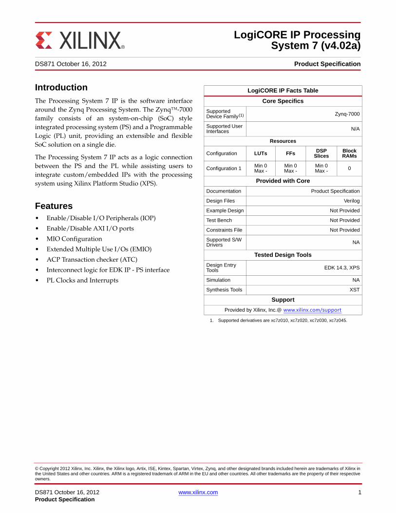
LogiCORE IP Facts Table
Core Specifics
Supported Device Family(1)
1. Supported derivatives are xc7z010, xc7z020, xc7z030, xc7z045.
Zynq-7000
Supported User Interfaces N/A
Resources
Configuration LUTs FFs DSP Slices
Block RAMs
Configuration 1 Min 0Max -
Min 0Max -
Min 0Max - 0
Provided with Core
Documentation Product Specification
Design Files Verilog
Example Design Not Provided
Test Bench Not Provided
Constraints File Not Provided
Supported S/W Drivers NA
Tested Design Tools
Design Entry Tools EDK 14.3, XPS
Simulation NA
Synthesis Tools XST
Support
Provided by Xilinx, Inc.@ www.xilinx.com/support
DS871 October 16, 2012 www.xilinx.com 2Product Specification
LogiCORE IP Processing System 7 (v4.02a)
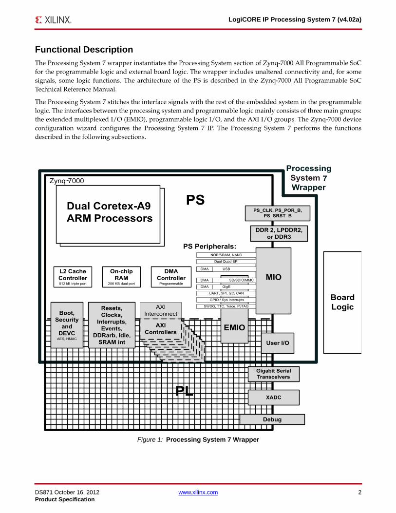
Functional DescriptionThe Processing System 7 wrapper instantiates the Processing System section of Zynq-7000 All Programmable SoCfor the programmable logic and external board logic. The wrapper includes unaltered connectivity and, for somesignals, some logic functions. The architecture of the PS is described in the Zynq-7000 All Programmable SoCTechnical Reference Manual.
The Processing System 7 stitches the interface signals with the rest of the embedded system in the programmablelogic. The interfaces between the processing system and programmable logic mainly consists of three main groups:the extended multiplexed I/O (EMIO), programmable logic I/O, and the AXI I/O groups. The Zynq-7000 deviceconfiguration wizard configures the Processing System 7 IP. The Processing System 7 performs the functionsdescribed in the following subsections.
X-Ref Target - Figure 1
Figure 1: Processing System 7 Wrapper
DS871 October 16, 2012 www.xilinx.com 3Product Specification
LogiCORE IP Processing System 7 (v4.02a)
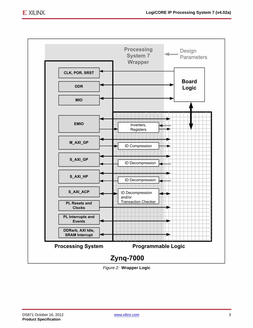
X-Ref Target - Figure 2
Figure 2: Wrapper Logic
DS871 October 16, 2012 www.xilinx.com 4Product Specification
LogiCORE IP Processing System 7 (v4.02a)
Connectivity
DDR, MIO, POR/CLK/SRST ports are unaltered.
• The width of GPIO ports on EMIO are user selectable via the C_EMIO_GPIO_WIDTH parameter .
• TTC clocks and TTC WAVEO are made individual signals instead of a (2:0) array
• FCLK are also made individual signals instead of the array FCLKCLK (3:0)
• IRQP2F are made individual signals IRQ_P2F_DMAC_ABORT, IRQ_P2F_DMAC7, IRQ_P2F_DMAC6, IRQ_P2F_DMAC5, IRQ_P2F_DMAC4, IRQ_P2F_DMAC3, IRQ_P2F_DMAC2, IRQ_P2F_DMAC1, IRQ_P2F_DMAC0, IRQ_P2F_SMC, IRQ_P2F_QSPI, IRQ_P2F_CTI, IRQ_P2F_GPIO, IRQ_P2F_USB0, IRQ_P2F_ENET0, IRQ_P2F_ENET_WAKE0, IRQ_P2F_SDIO0, IRQ_P2F_I2C0, IRQ_P2F_SPI0, IRQ_P2F_UART0, IRQ_P2F_CAN0, IRQ_P2F_USB1, IRQ_P2F_ENET1, IRQ_P2F_ENET_WAKE1, IRQ_P2F_SDIO1, IRQ_P2F_I2C1, IRQ_P2F_SPI1, IRQ_P2F_UART1, IRQ_P2F_CAN1
• SPI or SPI* SSON are made individual signals SPI*_SS2_O, SPI*_SS1_O, SPI*_SS_O.
AXI Interface IDs and Remap
ID compression and decompression is available for all the AXI interfaces. ID compress/decompress logic forM_AXI ports are dependent on the C_M_AXI_GP*_ENABLE_STATIC_REMAP parameter. If this parameter is 1,M_AXI THREAD ID widths are compressed to 6 bits; otherwise it is 12 bits. For the rest of the slaves, AXI interfacesID width can be anything between 1 to the max ID width for a particular interface depending on user selection.
In general, enabling static remapping reduces resources, especially at a higher PL slave count versus a potential PLAXI maximum frequency impact. Remapping must be disabled when a PL master accesses PL slaves through thePS instead of through the PL directly.
ACP Transaction Checker (ATC)
The ACP Transaction checker detects if an ACP write transaction uses the correct type, size, and length qualifiers.It implements a command pipelined stage and stalls command flow if the check fails. The functions performed byATC are:
• Checks if transaction is coherent.
• Checks transaction cacheline address.
• Checks transaction burst type, size and length.
• Stores transaction information like ID, burst type, size, and length in FIFO.
• Throttles transaction and stalls commands if FIFO is full.
• Delays pipelined commands until all data for a transaction has flowed through.
• Generates AXI User Signal for ACP
I/O Peripherals (IOP)
I/O Peripherals (IOP) include QSPI, NOR/NAND Flash, UART, I2C, SPI, SDIO, GPIO, CAN, USB, and Ethernet.The interfaces for these IOPs can be routed to MIO ports and the EMIO interfaces as described in the Zynq-7000Extensible Processing Platform Technical Reference Manual (UG585).
MIO Ports
The Zynq-7000 FPGA All Programmable SoC design tools are used to configure the Zynq-7000 processing systemMIO ports. There are up to 54 MIO ports available from the processing system. The wizard allows the user to choosethe peripheral ports to be connected to MIO ports.
DS871 October 16, 2012 www.xilinx.com 5Product Specification
LogiCORE IP Processing System 7 (v4.02a)
Extended MIO (EMIO) Ports
Because there are only up to 54 MIO ports available to users, many peripheral I/O ports beyond these can still berouted to the programmable logic through the EMIO interface. Alternative routing for IOP interfaces throughprogrammable logic enables users to take full advantage of the IOP available in the processing system. The EMIOfor I2C, SPI, Ethernet MDIO, PJTAG, SDIO, GPIO 3-state enable signals are inverted in the processing System 7 IP.
The processing_system7 allows users to select GPIO up to 64 bits. Processing System 7 has control logic to adjustuser-selected width to flow into PS7.
GigE MAC (Registering)
The Ethernet GMII TXD, TX_EN, TX_ER, COL and CRS signals are registered on TX_CLK, while the RXD, RX_DV andRX_ER signals are registered on RX_CLK.
Fabric Trace Monitor (FTM)
The fabric trace monitor (FTM) signals such as FTM TRACE DATA, VALID and ATID signals are also registered onFTMD_TRACEIN_CLK.
Signal Inverters (3-State)
Only the 3-state (*_T_n) signals are inverted. However SDIO{0,1}_CMD_T and SDIO{0,1}_DATA_T are invertedonly if C_PS7_SI_REV is not a CES 7020 silicon.
AXI I/O Interfaces
The AXI I/O interface group contains AXI interfaces between the Processing System and the programmable logic.The AXI interfaces include two general purpose master ports, two general purpose slave ports along with four highperformance ports and an accelerator coherency port (ACP). The ID widths of the slave ports are variable andProcessing System 7 controls the ID width of these ports based on a user parameter. ACP transactions are monitoredby the ACP transactions checker (ATC).
Logic for EDK IP - Processing System Interface
Processing System 7 allows the user to add EDK IPs in the programmable logic to be interfaced with the processingsystem. AXI Interfaces can be used by an AXI3-compliant master or slave to be connected to the ARM® system.Xilinx provided PL-based IPs use AXI4 or AXI4-Lite and require conversion, typically through an AXI Interconnectcore. Custom DMA functions can be implemented in the PL to oversee data movement irrespective of theprocessor’s intervention. Processing system interrupts from IOPs are available to custom master interfaces in PL.The clock throttling FCLK_CLKTRIG0_N, FCLK_CLKTRIG1_N, FCLK_CLKTRIG2_N, FCLK_CLKTRIG3_N ports arereserved and not supported.
DS871 October 16, 2012 www.xilinx.com 6Product Specification
LogiCORE IP Processing System 7 (v4.02a)
Programmable Logic Clocks and Interrupts
The Processing System 7 employs logic to handle PL interrupts, the number which varies from 1 to 16 depending onthe user selection. The number of interrupts connected to IRQ_F2P are calculated and the logic ensures the correctorder of an interrupt assignment.
The processing system provides four clocks to the PL. Processing System 7 enables configuration of these clocks tobe used in the PL. Processing System 7 inserts a BUFG for each of the PL clocks via parameters similar toC_FCLK_CLK0_BUF.
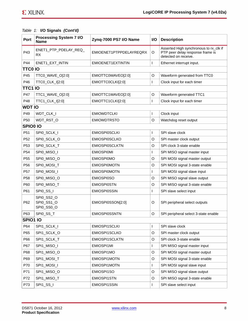
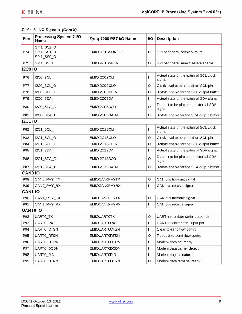
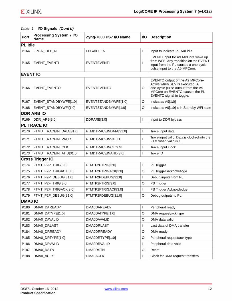
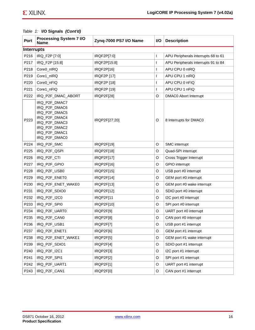
I/O SignalsThe I/O signals for the design are listed in Table 1.
Table 1: I/O Signals
Port Processing System 7 I/O Name Zynq-7000 PS7 I/O Name I/O Description
ENET0 IOP1 ENET0_GMII_RX_CLK EMIOENET0GMIIRXCLK I Receive clock
P2 ENET0_GMII_CRS EMIOENET0GMIICRS I Carrier sense from the PHY
P2 ENET0_GMII_CRS EMIOENET0GMIICRS I Carrier sense from the PHY
P3 ENET0_GMII_COL EMIOENET0GMIICOL I Collision detect from the PHY
P4 ENET0_GMII_RXD[7:0] EMIOENET0GMIIRXD[7:0] I Receive data from the PHY
P5 ENET0_GMII_RX_ER EMIOENET0GMIIRXER I Receive error signal from the PHY
P6 ENET0_GMII_TX_CLK EMIOENET0GMIITXCLK I Receive data valid signal from the PHY
P7 ENET0_GMII_TXD[7:0] EMIOENET0GMIITXD[7:0] O Transmit clock
P8 ENET0_GMII_TX_EN EMIOENET0GMIITXEN O Transmit data to the PHY
P9 ENET0_GMII_TX_ER EMIOENET0GMIITXER O Transmit enable to the PHY
P10 ENET0_MDIO_MDC EMIOENET0MDIOMDC O Management data clock to pin
P11 ENET0_MDIO_I EMIOENET0MDIOI I Management data input from MDIO pin
P12 ENET0_MDIO_O EMIOENET0MDIOO O Management data output to MDIO pin
P13 ENET0_MDIO_T EMIOENET0MDIOTN O Management data active-Low 3-state enable to MDIO pin, active-Low.
P14 ENET0_PTP_SYNC_FRAME_TX EMIOENET0PTPSYNCFRAMETX O Asserted High synchronous to tx_clk if
PTP sync frame is detected on transmit.
P15 ENET0_PTP_DELAY_REQ_TX EMIOENET0PTPDELAYREQTX O
Asserted High synchronous to tx_clk if PTP delay request frame is detected on transmit.
P16ENET0_PTP_PDELAY_REQ_TX
EMIOENET0PTPPDELAYREQTX OAsserted High synchronous to tx_clk if PTP peer delay request frame is detected on transmit.
P17 ENET0_PTP_PDELAY_RESP_TX EMIOENET0PTPPDELAYRESPTX O
Asserted High synchronous to tx_clk if PTP peer delay response frame is detected on transmit.
P18 ENET0_SOF_TX EMIOENET0SOFTX O Asserted High synchronous to rx_clk if PTP sync frame is detected on receive.
DS871 October 16, 2012 www.xilinx.com 7Product Specification
LogiCORE IP Processing System 7 (v4.02a)
P19ENET0_PTP_SYNC_FRAME_RX
EMIOENET0PTPSYNCFRAMERX OAsserted High synchronous to rx_clk if PTP delay request frame is detected on receive.
P20 ENET0_PTP_DELAY_REQ_RX EMIOENET0PTPDELAYREQRX O
Asserted High synchronous to rx_clk if PTP peer delay request frame is detected on receive.
P21ENET0_PTP_PDELAY_REQ_RX
EMIOENET0PTPPDELAYREQRX OAsserted High synchronous to rx_clk if PTP peer delay response frame is detected on receive.
P22 ENET0_EXT_INTIN EMIOENET0EXTINTIN I Ethernet interrupt input
ENET1 IOP23 ENET1_GMII_RX_CLK EMIOENET1GMIIRXCLK I Receive clock
P24 ENET1_GMII_CRS EMIOENET1GMIICRS I Carrier sense from the PHY
P25 ENET1_GMII_COL EMIOENET1GMIICOL I Collision detect from the PHY
P26 ENET1_GMII_RXD[7:0] EMIOENET1GMIIRXD[7:0] I Receive data from the PHY
P27 ENET1_GMII_RX_ER EMIOENET1GMIIRXER I Receive error signal from the PHY
P28 ENET1_GMII_TX_CLK EMIOENET1GMIITXCLK I Receive data valid signal from the PHY
P29 ENET1_GMII_TXD[7:0] EMIOENET1GMIITXD[7:0] O Transmit clock
P30 ENET1_GMII_TXEN EMIOENET1GMIITXEN O Transmit data to the PHY
P31 ENET1_GMII_TX_ER EMIOENET1GMIITXER O Transmit enable to the PHY
P32 ENET1_MDIO_MDC EMIOENET1MDIOMDC O Management data clock to pin
P33 ENET1_MDIO_I EMIOENET1MDIOI I Management data input from MDIO pin
P34 ENET1_MDIO_O EMIOENET1MDIOO O Management data output to MDIO pin
P35 ENET1_MDIO_T EMIOENET1MDIOTN O Management data active-Low 3-state enable to MDIO pin, active-Low
P36ENET1_PTP_SYNC_FRAME_TX
EMIOENET1PTPSYNCFRAMETX O Asserted High synchronous to tx_clk if PTP sync frame is detected on transmit.
P37ENET1_PTP_DELAY_REQ_TX
EMIOENET1PTPDELAYREQTX OAsserted High synchronous to tx_clk if PTP delay request frame is detected on transmit.
P38ENET1_PTP_PDELAY_REQ_TX
EMIOENET1PTPPDELAYREQTX OAsserted High synchronous to tx_clk if PTP peer delay request frame is detected on transmit.
P39ENET1_PTP_PDELAY_RESP_TX
EMIOENET1PTPPDELAYRESPTX OAsserted High synchronous to tx_clk if PTP peer delay response frame is detected on transmit.
P40 ENET1_SOF_TX EMIOENET1SOFTX O Asserted High synchronous to rx_clk if PTP sync frame is detected on receive.
P41ENET1_PTP_SYNC_FRAME_RX
EMIOENET1PTPSYNCFRAMERX OAsserted High synchronous to rx_clk if PTP delay request frame is detected on receive.
P42 ENET1_PTP_DELAY_REQRX EMIOENET1PTPDELAYREQRX OAsserted High synchronous to rx_clk if PTP peer delay request frame is detected on receive.
Table 1: I/O Signals (Cont’d)
Port Processing System 7 I/O Name Zynq-7000 PS7 I/O Name I/O Description
DS871 October 16, 2012 www.xilinx.com 8Product Specification
LogiCORE IP Processing System 7 (v4.02a)
P43ENET1_PTP_PDELAY_REQ_RX
EMIOENET1PTPPDELAYREQRX OAsserted High synchronous to rx_clk if PTP peer delay response frame is detected on receive.
P44 ENET1_EXT_INTIN EMIOENET1EXTINTIN I Ethernet interrupt input.
TTC0 IOP45 TTC0_WAVE_O[2:0] EMIOTTC0WAVEO[2:0] O Waveform generated from TTC0
P46 TTC0_CLK_I[2:0] EMIOTTC0CLKI[2:0] I Clock input for each timer
TTC1 IOP47 TTC1_WAVE_O[2:0] EMIOTTC1WAVEO[2:0] O Waveform generated TTC1
P48 TTC1_CLK_I[2:0] EMIOTTC1CLKI[2:0] I Clock input for each timer
WDT IOP49 WDT_CLK_I EMIOWDTCLKI I Clock input
P50 WDT_RST_O EMIOWDTRSTO O Watchdog reset output
SPIO0 IOP51 SPI0_SCLK_I EMIOSPI0SCLKI I SPI slave clock
P52 SPI0_SCLK_O EMIOSPI0SCLKO O SPI master clock output
P53 SPI0_SCLK_T EMIOSPI0SCLKTN O SPI clock 3-state enable
P54 SPI0_MISO_I EMIOSPI0MI I SPI MISO signal master input
P55 SPI0_MISO_O EMIOSPI0MO O SPI MOSI signal master output
P56 SPI0_MOSI_T EMIOSPI0MOTN O SPI MOSI signal 3-state enable
P57 SPI0_MOSI_I EMIOSPI0MOTN I SPI MOSI signal slave input
P58 SPI0_MISO_O EMIOSPI0SO O SPI MISO signal slave output
P60 SPI0_MISO_T EMIOSPI0STN O SPI MISO signal 3-state enable
P61 SPI0_SS_I EMIOSPI0SSIN I SPI slave select input
P62SPI0_SS2_OSPI0_SS1_OSPI0_SS0_O
EMIOSPI0SSON[2:0] O SPI peripheral select outputs
P63 SPI0_SS_T EMIOSPI0SSNTN O SPI peripheral select 3-state enable
SPIO1 IOP64 SPI1_SCLK_I EMIOSPI1SCLKI I SPI slave clock
P65 SPI1_SCLK_O EMIOSPI1SCLKO O SPI master clock output
P66 SPI1_SCLK_T EMIOSPI1SCLKTN O SPI clock 3-state enable
P67 SPI1_MISO_I EMIOSPI1MI I SPI MISO signal master input
P68 SPI1_MISO_O EMIOSPI1MO O SPI MOSI signal master output
P69 SPI1_MOSI_T EMIOSPI1MOTN O SPI MOSI signal 3-state enable
P70 SPI1_MOSI_I EMIOSPI1MOTN I SPI MOSI signal slave input
P71 SPI1_MISO_O EMIOSPI1SO O SPI MISO signal slave output
P72 SPI1_MISO_T EMIOSPI1STN O SPI MISO signal 3-state enable
P73 SPI1_SS_I EMIOSPI1SSIN I SPI slave select input
Table 1: I/O Signals (Cont’d)
Port Processing System 7 I/O Name Zynq-7000 PS7 I/O Name I/O Description
DS871 October 16, 2012 www.xilinx.com 9Product Specification
LogiCORE IP Processing System 7 (v4.02a)
P74SPI1_SS2_OSPI1_SS1_OSPI1_SS0_O
EMIOSPI1SSON[2:0] O SPI peripheral select outputs
P75 SPI1_SS_T EMIOSPI1SSNTN O SPI peripheral select 3-state enable
I2C0 IO
P76 I2C0_SCL_I EMIOI2C0SCLI I Actual state of the external SCL clock signal
P77 I2C0_SCL_O EMIOI2C0SCLO O Clock level to be placed on SCL pin
P78 I2C0_SCL_T EMIOI2C0SCLTN O 3-state enable for the SCL output buffer
P79 I2C0_SDA_I EMIOI2C0SDAI I Actual state of the external SDA signal
P80 I2C0_SDA_O EMIOI2C0SDAO O Data bit to be placed on external SDA signal
P81 I2C0_SDA_T EMIOI2C0SDATN O 3-state enable for the SDA output buffer
I2C1 IO
P82 I2C1_SCL_I EMIOI2C1SCLI I Actual state of the external SCL clock signal
P83 I2C1_SCL_O EMIOI2C1SCLO O Clock level to be placed on SCL pin
P84 I2C1_SCL_T EMIOI2C1SCLTN O 3-state enable for the SCL output buffer
P85 I2C1_SDA_I EMIOI2C1SDAI I Actual state of the external SDA signal
P86 I2C1_SDA_O EMIOI2C1SDAO O Data bit to be placed on external SDA signal
P87 I2C1_SDA_T EMIOI2C1SDATN O 3-state enable for the SDA output buffer
CAN0 IOP88 CAN0_PHY_TX EMIOCAN0PHYTX O CAN bus transmit signal
P89 CAN0_PHY_RX EMIOCAN0PHYRX I CAN bus receive signal
CAN1 IOP90 CAN1_PHY_TX EMIOCAN1PHYTX O CAN bus transmit signal
P91 CAN1_PHY_RX EMIOCAN1PHYRX I CAN bus receive signal
UART0 IOP92 UART0_TX EMIOUART0TX O UART transmitter serial output pin
P93 UART0_RX EMIOUART0RX I UART receiver serial input pin
P94 UART0_CTSN EMIOUART0CTSN I Clear-to-send flow control
P95 UART0_RTSN EMIOUART0RTSN O Request-to-send flow control
P96 UART0_DSRN EMIOUART0DSRN I Modem data set ready
P97 UART0_DCDN EMIOUART0DCDN I Modem data carrier detect
P98 UART0_RIN EMIOUART0RIN I Modem ring indicator
P99 UART0_DTRN EMIOUART0DTRN O Modem data terminal ready
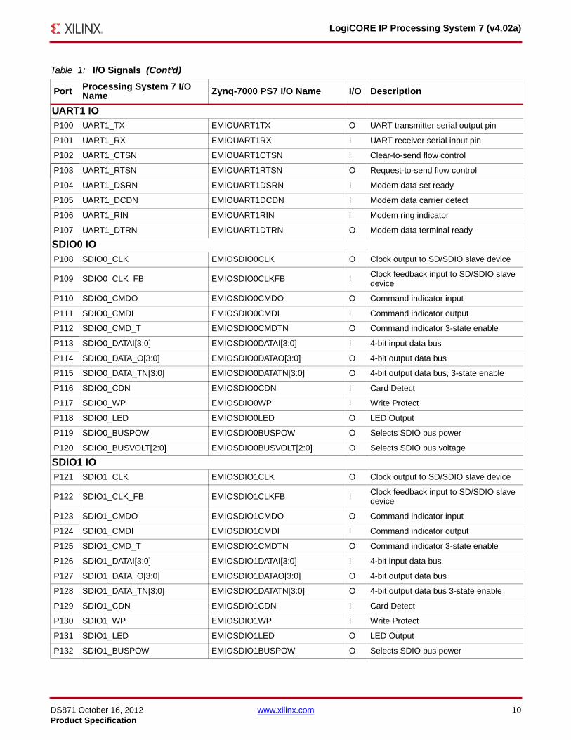
Table 1: I/O Signals (Cont’d)
Port Processing System 7 I/O Name Zynq-7000 PS7 I/O Name I/O Description
DS871 October 16, 2012 www.xilinx.com 10Product Specification
LogiCORE IP Processing System 7 (v4.02a)
UART1 IOP100 UART1_TX EMIOUART1TX O UART transmitter serial output pin
P101 UART1_RX EMIOUART1RX I UART receiver serial input pin
P102 UART1_CTSN EMIOUART1CTSN I Clear-to-send flow control
P103 UART1_RTSN EMIOUART1RTSN O Request-to-send flow control
P104 UART1_DSRN EMIOUART1DSRN I Modem data set ready
P105 UART1_DCDN EMIOUART1DCDN I Modem data carrier detect
P106 UART1_RIN EMIOUART1RIN I Modem ring indicator
P107 UART1_DTRN EMIOUART1DTRN O Modem data terminal ready
SDIO0 IOP108 SDIO0_CLK EMIOSDIO0CLK O Clock output to SD/SDIO slave device
P109 SDIO0_CLK_FB EMIOSDIO0CLKFB I Clock feedback input to SD/SDIO slave device
P110 SDIO0_CMDO EMIOSDIO0CMDO O Command indicator input
P111 SDIO0_CMDI EMIOSDIO0CMDI I Command indicator output
P112 SDIO0_CMD_T EMIOSDIO0CMDTN O Command indicator 3-state enable
P113 SDIO0_DATAI[3:0] EMIOSDIO0DATAI[3:0] I 4-bit input data bus
P114 SDIO0_DATA_O[3:0] EMIOSDIO0DATAO[3:0] O 4-bit output data bus
P115 SDIO0_DATA_TN[3:0] EMIOSDIO0DATATN[3:0] O 4-bit output data bus, 3-state enable
P116 SDIO0_CDN EMIOSDIO0CDN I Card Detect
P117 SDIO0_WP EMIOSDIO0WP I Write Protect
P118 SDIO0_LED EMIOSDIO0LED O LED Output
P119 SDIO0_BUSPOW EMIOSDIO0BUSPOW O Selects SDIO bus power
P120 SDIO0_BUSVOLT[2:0] EMIOSDIO0BUSVOLT[2:0] O Selects SDIO bus voltage
SDIO1 IOP121 SDIO1_CLK EMIOSDIO1CLK O Clock output to SD/SDIO slave device
P122 SDIO1_CLK_FB EMIOSDIO1CLKFB I Clock feedback input to SD/SDIO slave device
P123 SDIO1_CMDO EMIOSDIO1CMDO O Command indicator input
P124 SDIO1_CMDI EMIOSDIO1CMDI I Command indicator output
P125 SDIO1_CMD_T EMIOSDIO1CMDTN O Command indicator 3-state enable
P126 SDIO1_DATAI[3:0] EMIOSDIO1DATAI[3:0] I 4-bit input data bus
P127 SDIO1_DATA_O[3:0] EMIOSDIO1DATAO[3:0] O 4-bit output data bus
P128 SDIO1_DATA_TN[3:0] EMIOSDIO1DATATN[3:0] O 4-bit output data bus 3-state enable
P129 SDIO1_CDN EMIOSDIO1CDN I Card Detect
P130 SDIO1_WP EMIOSDIO1WP I Write Protect
P131 SDIO1_LED EMIOSDIO1LED O LED Output
P132 SDIO1_BUSPOW EMIOSDIO1BUSPOW O Selects SDIO bus power
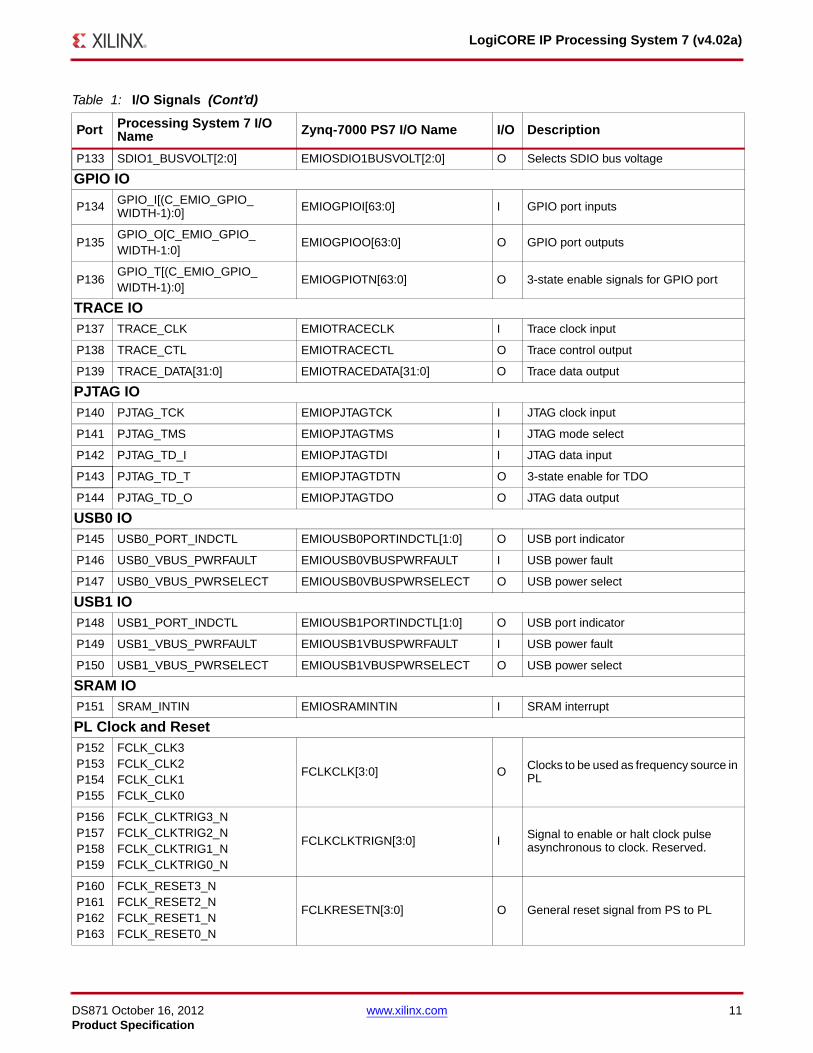
Table 1: I/O Signals (Cont’d)
Port Processing System 7 I/O Name Zynq-7000 PS7 I/O Name I/O Description
DS871 October 16, 2012 www.xilinx.com 11Product Specification
LogiCORE IP Processing System 7 (v4.02a)
P133 SDIO1_BUSVOLT[2:0] EMIOSDIO1BUSVOLT[2:0] O Selects SDIO bus voltage
GPIO IO
P134 GPIO_I[(C_EMIO_GPIO_WIDTH-1):0] EMIOGPIOI[63:0] I GPIO port inputs
P135GPIO_O[C_EMIO_GPIO_WIDTH-1:0]
EMIOGPIOO[63:0] O GPIO port outputs
P136GPIO_T[(C_EMIO_GPIO_WIDTH-1):0]
EMIOGPIOTN[63:0] O 3-state enable signals for GPIO port
TRACE IOP137 TRACE_CLK EMIOTRACECLK I Trace clock input
P138 TRACE_CTL EMIOTRACECTL O Trace control output
P139 TRACE_DATA[31:0] EMIOTRACEDATA[31:0] O Trace data output
PJTAG IOP140 PJTAG_TCK EMIOPJTAGTCK I JTAG clock input
P141 PJTAG_TMS EMIOPJTAGTMS I JTAG mode select
P142 PJTAG_TD_I EMIOPJTAGTDI I JTAG data input
P143 PJTAG_TD_T EMIOPJTAGTDTN O 3-state enable for TDO
P144 PJTAG_TD_O EMIOPJTAGTDO O JTAG data output
USB0 IOP145 USB0_PORT_INDCTL EMIOUSB0PORTINDCTL[1:0] O USB port indicator
P146 USB0_VBUS_PWRFAULT EMIOUSB0VBUSPWRFAULT I USB power fault
P147 USB0_VBUS_PWRSELECT EMIOUSB0VBUSPWRSELECT O USB power select
USB1 IOP148 USB1_PORT_INDCTL EMIOUSB1PORTINDCTL[1:0] O USB port indicator
P149 USB1_VBUS_PWRFAULT EMIOUSB1VBUSPWRFAULT I USB power fault
P150 USB1_VBUS_PWRSELECT EMIOUSB1VBUSPWRSELECT O USB power select
SRAM IOP151 SRAM_INTIN EMIOSRAMINTIN I SRAM interrupt
PL Clock and ResetP152P153P154P155
FCLK_CLK3FCLK_CLK2FCLK_CLK1FCLK_CLK0
FCLKCLK[3:0] O Clocks to be used as frequency source in PL
P156P157P158P159
FCLK_CLKTRIG3_NFCLK_CLKTRIG2_NFCLK_CLKTRIG1_NFCLK_CLKTRIG0_N
FCLKCLKTRIGN[3:0] I Signal to enable or halt clock pulse asynchronous to clock. Reserved.
P160P161P162P163
FCLK_RESET3_NFCLK_RESET2_NFCLK_RESET1_NFCLK_RESET0_N
FCLKRESETN[3:0] O General reset signal from PS to PL
Table 1: I/O Signals (Cont’d)
Port Processing System 7 I/O Name Zynq-7000 PS7 I/O Name I/O Description
DS871 October 16, 2012 www.xilinx.com 12Product Specification
LogiCORE IP Processing System 7 (v4.02a)
PL IdleP164 FPGA_IDLE_N FPGAIDLEN I Input to indicate PL AXI idle
P165 EVENT_EVENTI EVENTEVENTI I
EVENTI input for A9 MPCore wake up from WFE. Any transition on the EVENTI input from the PL causes a one-cycle pulse input to the A9 MPCore.
EVENT IO
P166 EVENT_EVENTO EVENTEVENTO O
EVENTO output of the A9 MPCore- Active when SEV is executed. A one-cycle pulse output from the A9 MPCore on EVENTO causes the PL EVENTO signal to toggle.
P167 EVENT_STANDBYWFE[1:0] EVENTSTANDBYWFE[1:0] O Indicates A9[1:0]
P168 EVENT_STANDBYWFI[1:0] EVENTSTANDBYWFI[1:0] O Indicates A9[1:0] is in Standby WFI state
DDR ARB IOP169 DDR_ARB[3:0] DDRARB[3:0] I Input to DDR bypass
PL TRACE IOP170 FTMD_TRACEIN_DATA[31:0] FTMDTRACEINDATA[31:0] I Trace input data
P171 FTMD_TRACEIN_VALID FTMDTRACEINVALID I Trace input valid. Data is clocked into the FTM when valid is 1.
P172 FTMD_TRACEIN_CLK FTMDTRACEINCLOCK I Trace input clock
P173 FTMD_TRACEIN_ATID[31:0] FTMDTRACEINATID[3:0] I Trace ID
Cross Trigger IOP174 FTMT_F2P_TRIG[3:0] FTMTF2PTRIG[3:0] I PL Trigger
P175 FTMT_F2P_TRIGACK[3:0] FTMTF2PTRIGACK[3:0] O PL Trigger Acknowledge
P176 FTMT_F2P_DEBUG[31:0] FTMTF2PDEBUG[31:0] I Debug inputs from PL
P177 FTMT_P2F_TRIG[3:0] FTMTP2FTRIG[3:0] O PS Trigger
P178 FTMT_P2F_TRIGACK[3:0] FTMTP2FTRIGACK[3:0] I PS Trigger Acknowledge
P179 FTMT_P2F_DEBUG[31:0] FTMTP2FDEBUG[31:0] O Debug outputs to PL
DMA0 IOP180 DMA0_DAREADY DMA0DAREADY I Peripheral ready
P181 DMA0_DATYPE[1:0] DMA0DATYPE[1:0] O DMA request/ack type
P182 DMA0_DAVALID DMA0DAVALID O DMA data valid
P183 DMA0_DRLAST DMA0DRLAST I Last data of DMA transfer
P184 DMA0_DRREADY DMA0DRREADY O DMA ready
P185 DMA0_DRTYPE[1:0] DMA0DRTYPE[1:0] O Peripheral request/ack type
P186 DMA0_DRVALID DMA0DRVALID I Peripheral data valid
P187 DMA0_RSTN DMA0RSTN O Reset
P188 DMA0_ACLK DMA0ACLK I Clock for DMA request transfers
Table 1: I/O Signals (Cont’d)
Port Processing System 7 I/O Name Zynq-7000 PS7 I/O Name I/O Description
DS871 October 16, 2012 www.xilinx.com 13Product Specification
LogiCORE IP Processing System 7 (v4.02a)
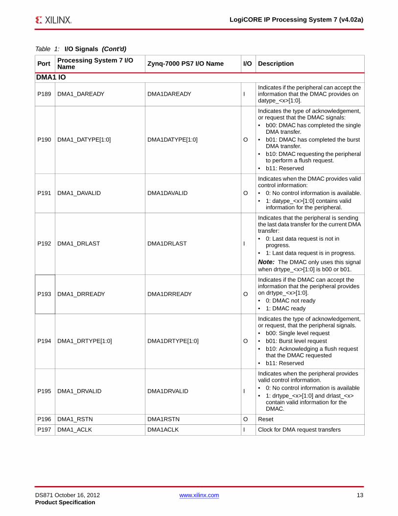
DMA1 IO
P189 DMA1_DAREADY DMA1DAREADY IIndicates if the peripheral can accept the information that the DMAC provides on datype_<x>[1:0].
P190 DMA1_DATYPE[1:0] DMA1DATYPE[1:0] O
Indicates the type of acknowledgement, or request that the DMAC signals:• b00: DMAC has completed the single
DMA transfer.• b01: DMAC has completed the burst
DMA transfer.• b10: DMAC requesting the peripheral
to perform a flush request.• b11: Reserved
P191 DMA1_DAVALID DMA1DAVALID O
Indicates when the DMAC provides valid control information:• 0: No control information is available.• 1: datype_<x>[1:0] contains valid
information for the peripheral.
P192 DMA1_DRLAST DMA1DRLAST I
Indicates that the peripheral is sending the last data transfer for the current DMA transfer:• 0: Last data request is not in
progress.• 1: Last data request is in progress.
Note: The DMAC only uses this signal when drtype_<x>[1:0] is b00 or b01.
P193 DMA1_DRREADY DMA1DRREADY O
Indicates if the DMAC can accept the information that the peripheral provides on drtype_<x>[1:0].• 0: DMAC not ready• 1: DMAC ready
P194 DMA1_DRTYPE[1:0] DMA1DRTYPE[1:0] O
Indicates the type of acknowledgement, or request, that the peripheral signals.• b00: Single level request• b01: Burst level request• b10: Acknowledging a flush request
that the DMAC requested• b11: Reserved
P195 DMA1_DRVALID DMA1DRVALID I
Indicates when the peripheral provides valid control information.• 0: No control information is available• 1: drtype_<x>[1:0] and drlast_<x>
contain valid information for the DMAC.
P196 DMA1_RSTN DMA1RSTN O Reset
P197 DMA1_ACLK DMA1ACLK I Clock for DMA request transfers
Table 1: I/O Signals (Cont’d)
Port Processing System 7 I/O Name Zynq-7000 PS7 I/O Name I/O Description
DS871 October 16, 2012 www.xilinx.com 14Product Specification
LogiCORE IP Processing System 7 (v4.02a)
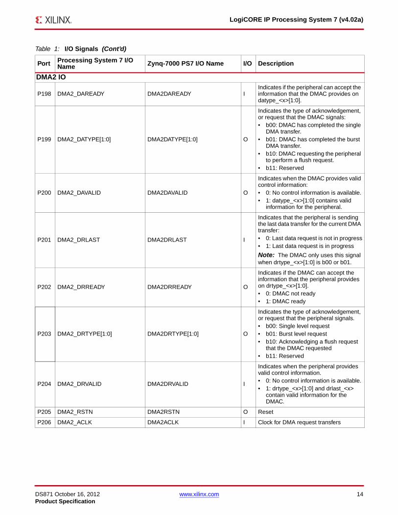
DMA2 IO
P198 DMA2_DAREADY DMA2DAREADY IIndicates if the peripheral can accept the information that the DMAC provides on datype_<x>[1:0].
P199 DMA2_DATYPE[1:0] DMA2DATYPE[1:0] O
Indicates the type of acknowledgement, or request that the DMAC signals:• b00: DMAC has completed the single
DMA transfer.• b01: DMAC has completed the burst
DMA transfer.• b10: DMAC requesting the peripheral
to perform a flush request.• b11: Reserved
P200 DMA2_DAVALID DMA2DAVALID O
Indicates when the DMAC provides valid control information:• 0: No control information is available.• 1: datype_<x>[1:0] contains valid
information for the peripheral.
P201 DMA2_DRLAST DMA2DRLAST I
Indicates that the peripheral is sending the last data transfer for the current DMA transfer:• 0: Last data request is not in progress• 1: Last data request is in progress
Note: The DMAC only uses this signal when drtype_<x>[1:0] is b00 or b01.
P202 DMA2_DRREADY DMA2DRREADY O
Indicates if the DMAC can accept the information that the peripheral provides on drtype_<x>[1:0].• 0: DMAC not ready• 1: DMAC ready
P203 DMA2_DRTYPE[1:0] DMA2DRTYPE[1:0] O
Indicates the type of acknowledgement, or request that the peripheral signals.• b00: Single level request• b01: Burst level request• b10: Acknowledging a flush request
that the DMAC requested• b11: Reserved
P204 DMA2_DRVALID DMA2DRVALID I
Indicates when the peripheral provides valid control information.• 0: No control information is available.• 1: drtype_<x>[1:0] and drlast_<x>
contain valid information for the DMAC.
P205 DMA2_RSTN DMA2RSTN O Reset
P206 DMA2_ACLK DMA2ACLK I Clock for DMA request transfers
Table 1: I/O Signals (Cont’d)
Port Processing System 7 I/O Name Zynq-7000 PS7 I/O Name I/O Description
DS871 October 16, 2012 www.xilinx.com 15Product Specification
LogiCORE IP Processing System 7 (v4.02a)
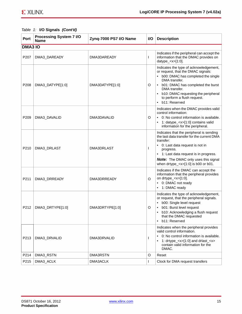
DMA3 IO
P207 DMA3_DAREADY DMA3DAREADY IIndicates if the peripheral can accept the information that the DMAC provides on datype_<x>[1:0].
P208 DMA3_DATYPE[1:0] DMA3DATYPE[1:0] O
Indicates the type of acknowledgement, or request, that the DMAC signals:• b00: DMAC has completed the single
DMA transfer.• b01: DMAC has completed the burst
DMA transfer.• b10: DMAC requesting the peripheral
to perform a flush request.• b11: Reserved
P209 DMA3_DAVALID DMA3DAVALID O
Indicates when the DMAC provides valid control information:• 0: No control information is available.• 1: datype_<x>[1:0] contains valid
information for the peripheral.
P210 DMA3_DRLAST DMA3DRLAST I
Indicates that the peripheral is sending the last data transfer for the current DMA transfer:• 0: Last data request is not in
progress.• 1: Last data request is in progress.
Note: The DMAC only uses this signal when drtype_<x>[1:0] is b00 or b01.
P211 DMA3_DRREADY DMA3DRREADY O
Indicates if the DMAC can accept the information that the peripheral provides on drtype_<x>[1:0].• 0: DMAC not ready• 1: DMAC ready
P212 DMA3_DRTYPE[1:0] DMA3DRTYPE[1:0] O
Indicates the type of acknowledgement, or request, that the peripheral signals.• b00: Single level request• b01: Burst level request• b10: Acknowledging a flush request
that the DMAC requested• b11: Reserved
P213 DMA3_DRVALID DMA3DRVALID I
Indicates when the peripheral provides valid control information.• 0: No control information is available.• 1: drtype_<x>[1:0] and drlast_<x>
contain valid information for the DMAC.
P214 DMA3_RSTN DMA3RSTN O Reset
P215 DMA3_ACLK DMA3ACLK I Clock for DMA request transfers
Table 1: I/O Signals (Cont’d)
Port Processing System 7 I/O Name Zynq-7000 PS7 I/O Name I/O Description
DS871 October 16, 2012 www.xilinx.com 16Product Specification
LogiCORE IP Processing System 7 (v4.02a)
InterruptsP216 IRQ_F2P [7:0] IRQF2P[7:0] I APU Peripherals interrupts 68 to 61
P217 IRQ_F2P [15:8] IRQF2P[15:8] I APU Peripherals interrupts 91 to 84
P218 Core0_nIRQ IRQF2P[16] I APU CPU 0 nIRQ
P219 Core1_nIRQ IRQF2P [17] I APU CPU 1 nIRQ
P220 Core0_nFIQ IRQF2P [18] I APU CPU 0 nFIQ
P221 Core1_nFIQ IRQF2P [19] I APU CPU 1 nFIQ
P222 IRQ_P2F_DMAC_ABORT IRQP2F[28] O DMAC0 Abort Interrupt
P223
IRQ_P2F_DMAC7IRQ_P2F_DMAC6IRQ_P2F_DMAC5IRQ_P2F_DMAC4IRQ_P2F_DMAC3IRQ_P2F_DMAC2IRQ_P2F_DMAC1IRQ_P2F_DMAC0
IRQP2F[27:20] O 8 Interrupts for DMAC0
P224 IRQ_P2F_SMC IRQP2F[19] O SMC interrupt
P225 IRQ_P2F_QSPI IRQP2F[18] O Quad-SPI interrupt
P226 IRQ_P2F_CTI IRQP2F[17] O Cross Trigger Interrupt
P227 IRQ_P2F_GPIO IRQP2F[16] O GPIO interrupt
P228 IRQ_P2F_USB0 IRQP2F[15] O USB port #0 interrupt
P229 IRQ_P2F_ENET0 IRQP2F[14] O GEM port #0 interrupt
P230 IRQ_P2F_ENET_WAKE0 IRQP2F[13] O GEM port #0 wake interrupt
P231 IRQ_P2F_SDIO0 IRQP2F[12] O SDIO port #0 interrupt
P232 IRQ_P2F_I2C0 IRQP2F[11 O I2C port #0 interrupt
P233 IRQ_P2F_SPI0 IRQP2F[10] O SPI port #0 interrupt
P234 IRQ_P2F_UART0 IRQP2F[9] O UART port #0 interrupt
P235 IRQ_P2F_CAN0 IRQP2F[8] O CAN port #0 interrupt
P236 IRQ_P2F_USB1 IRQP2F[7] O USB port #1 interrupt
P237 IRQ_P2F_ENET1 IRQP2F[6] O GEM port #1 interrupt
P238 IRQ_P2F_ENET_WAKE1 IRQP2F[5] O GEM port #1 wake interrupt
P239 IRQ_P2F_SDIO1 IRQP2F[4] O SDIO port #1 interrupt
P240 IRQ_P2F_I2C1 IRQP2F[3] O I2C port #1 interrupt
P241 IRQ_P2F_SPI1 IRQP2F[2] O SPI port #1 interrupt
P242 IRQ_P2F_UART1 IRQP2F[1] O UART port #1 interrupt
P243 IRQ_P2F_CAN1 IRQP2F[0] O CAN port #1 interrupt
Table 1: I/O Signals (Cont’d)
Port Processing System 7 I/O Name Zynq-7000 PS7 I/O Name I/O Description
DS871 October 16, 2012 www.xilinx.com 17Product Specification
LogiCORE IP Processing System 7 (v4.02a)
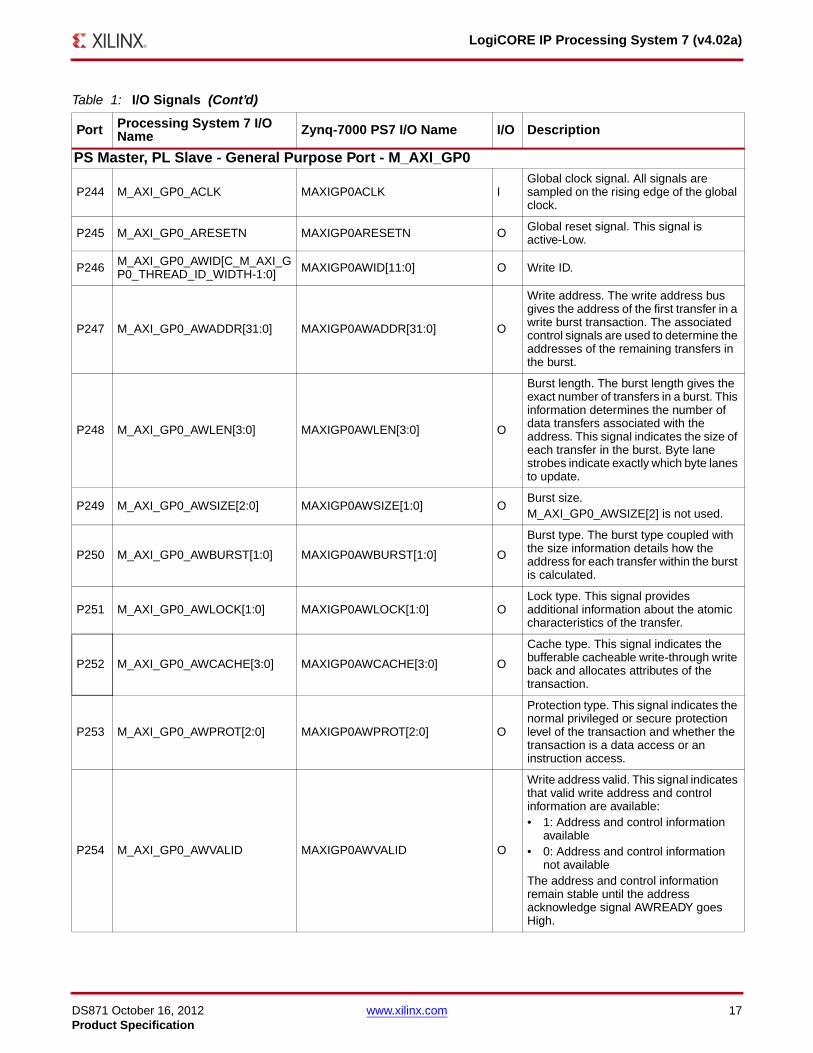
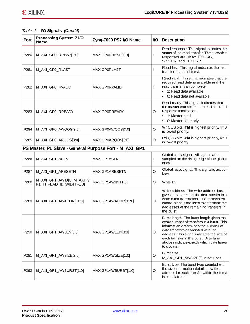
PS Master, PL Slave - General Purpose Port - M_AXI_GP0
P244 M_AXI_GP0_ACLK MAXIGP0ACLK IGlobal clock signal. All signals are sampled on the rising edge of the global clock.
P245 M_AXI_GP0_ARESETN MAXIGP0ARESETN O Global reset signal. This signal is active-Low.
P246 M_AXI_GP0_AWID[C_M_AXI_GP0_THREAD_ID_WIDTH-1:0] MAXIGP0AWID[11:0] O Write ID.
P247 M_AXI_GP0_AWADDR[31:0] MAXIGP0AWADDR[31:0] O
Write address. The write address bus gives the address of the first transfer in a write burst transaction. The associated control signals are used to determine the addresses of the remaining transfers in the burst.
P248 M_AXI_GP0_AWLEN[3:0] MAXIGP0AWLEN[3:0] O
Burst length. The burst length gives the exact number of transfers in a burst. This information determines the number of data transfers associated with the address. This signal indicates the size of each transfer in the burst. Byte lane strobes indicate exactly which byte lanes to update.
P249 M_AXI_GP0_AWSIZE[2:0] MAXIGP0AWSIZE[1:0] OBurst size.M_AXI_GP0_AWSIZE[2] is not used.
P250 M_AXI_GP0_AWBURST[1:0] MAXIGP0AWBURST[1:0] O
Burst type. The burst type coupled with the size information details how the address for each transfer within the burst is calculated.
P251 M_AXI_GP0_AWLOCK[1:0] MAXIGP0AWLOCK[1:0] OLock type. This signal provides additional information about the atomic characteristics of the transfer.
P252 M_AXI_GP0_AWCACHE[3:0] MAXIGP0AWCACHE[3:0] O
Cache type. This signal indicates the bufferable cacheable write-through write back and allocates attributes of the transaction.
P253 M_AXI_GP0_AWPROT[2:0] MAXIGP0AWPROT[2:0] O
Protection type. This signal indicates the normal privileged or secure protection level of the transaction and whether the transaction is a data access or an instruction access.
P254 M_AXI_GP0_AWVALID MAXIGP0AWVALID O
Write address valid. This signal indicates that valid write address and control information are available:• 1: Address and control information
available• 0: Address and control information
not availableThe address and control information remain stable until the address acknowledge signal AWREADY goes High.
Table 1: I/O Signals (Cont’d)
Port Processing System 7 I/O Name Zynq-7000 PS7 I/O Name I/O Description
DS871 October 16, 2012 www.xilinx.com 18Product Specification
LogiCORE IP Processing System 7 (v4.02a)
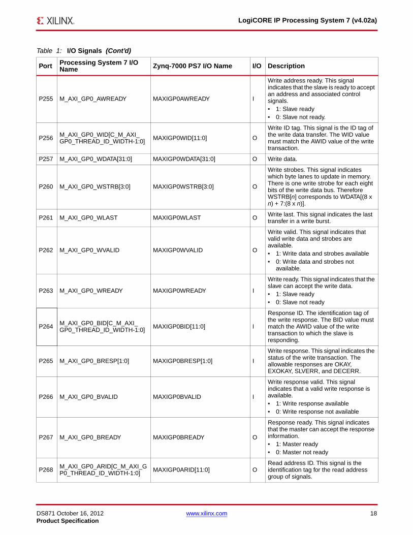
P255 M_AXI_GP0_AWREADY MAXIGP0AWREADY I
Write address ready. This signal indicates that the slave is ready to accept an address and associated control signals.• 1: Slave ready• 0: Slave not ready.
P256 M_AXI_GP0_WID[C_M_AXI_GP0_THREAD_ID_WIDTH-1:0] MAXIGP0WID[11:0] O
Write ID tag. This signal is the ID tag of the write data transfer. The WID value must match the AWID value of the write transaction.
P257 M_AXI_GP0_WDATA[31:0] MAXIGP0WDATA[31:0] O Write data.
P260 M_AXI_GP0_WSTRB[3:0] MAXIGP0WSTRB[3:0] O
Write strobes. This signal indicates which byte lanes to update in memory. There is one write strobe for each eight bits of the write data bus. Therefore WSTRB[n] corresponds to WDATA[(8 x n) + 7:(8 x n)].
P261 M_AXI_GP0_WLAST MAXIGP0WLAST O Write last. This signal indicates the last transfer in a write burst.
P262 M_AXI_GP0_WVALID MAXIGP0WVALID O
Write valid. This signal indicates that valid write data and strobes are available.• 1: Write data and strobes available• 0: Write data and strobes not
available.
P263 M_AXI_GP0_WREADY MAXIGP0WREADY I
Write ready. This signal indicates that the slave can accept the write data.• 1: Slave ready• 0: Slave not ready
P264 M_AXI_GP0_BID[C_M_AXI_GP0_THREAD_ID_WIDTH-1:0] MAXIGP0BID[11:0] I
Response ID. The identification tag of the write response. The BID value must match the AWID value of the write transaction to which the slave is responding.
P265 M_AXI_GP0_BRESP[1:0] MAXIGP0BRESP[1:0] I
Write response. This signal indicates the status of the write transaction. The allowable responses are OKAY, EXOKAY, SLVERR, and DECERR.
P266 M_AXI_GP0_BVALID MAXIGP0BVALID I
Write response valid. This signal indicates that a valid write response is available.• 1: Write response available• 0: Write response not available
P267 M_AXI_GP0_BREADY MAXIGP0BREADY O
Response ready. This signal indicates that the master can accept the response information.• 1: Master ready• 0: Master not ready
P268 M_AXI_GP0_ARID[C_M_AXI_GP0_THREAD_ID_WIDTH-1:0] MAXIGP0ARID[11:0] O
Read address ID. This signal is the identification tag for the read address group of signals.
Table 1: I/O Signals (Cont’d)
Port Processing System 7 I/O Name Zynq-7000 PS7 I/O Name I/O Description
DS871 October 16, 2012 www.xilinx.com 19Product Specification
LogiCORE IP Processing System 7 (v4.02a)
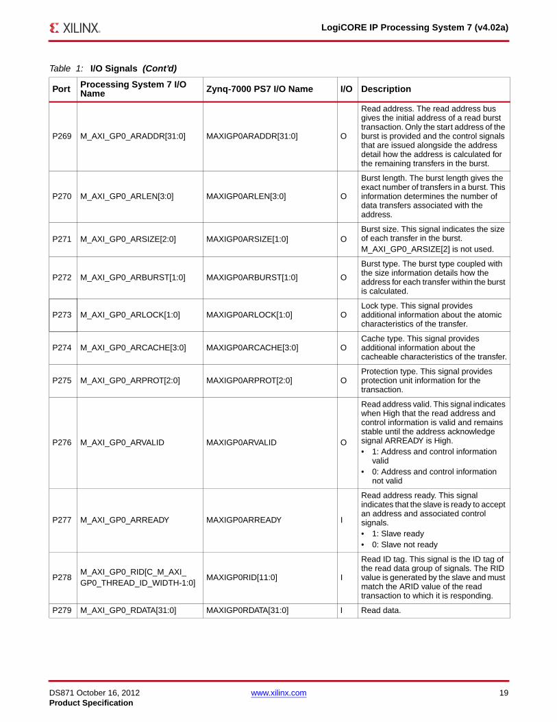
P269 M_AXI_GP0_ARADDR[31:0] MAXIGP0ARADDR[31:0] O
Read address. The read address bus gives the initial address of a read burst transaction. Only the start address of the burst is provided and the control signals that are issued alongside the address detail how the address is calculated for the remaining transfers in the burst.
P270 M_AXI_GP0_ARLEN[3:0] MAXIGP0ARLEN[3:0] O
Burst length. The burst length gives the exact number of transfers in a burst. This information determines the number of data transfers associated with the address.
P271 M_AXI_GP0_ARSIZE[2:0] MAXIGP0ARSIZE[1:0] OBurst size. This signal indicates the size of each transfer in the burst. M_AXI_GP0_ARSIZE[2] is not used.
P272 M_AXI_GP0_ARBURST[1:0] MAXIGP0ARBURST[1:0] O
Burst type. The burst type coupled with the size information details how the address for each transfer within the burst is calculated.
P273 M_AXI_GP0_ARLOCK[1:0] MAXIGP0ARLOCK[1:0] OLock type. This signal provides additional information about the atomic characteristics of the transfer.
P274 M_AXI_GP0_ARCACHE[3:0] MAXIGP0ARCACHE[3:0] OCache type. This signal provides additional information about the cacheable characteristics of the transfer.
P275 M_AXI_GP0_ARPROT[2:0] MAXIGP0ARPROT[2:0] OProtection type. This signal provides protection unit information for the transaction.
P276 M_AXI_GP0_ARVALID MAXIGP0ARVALID O
Read address valid. This signal indicates when High that the read address and control information is valid and remains stable until the address acknowledge signal ARREADY is High.• 1: Address and control information
valid• 0: Address and control information
not valid
P277 M_AXI_GP0_ARREADY MAXIGP0ARREADY I
Read address ready. This signal indicates that the slave is ready to accept an address and associated control signals.• 1: Slave ready• 0: Slave not ready
P278M_AXI_GP0_RID[C_M_AXI_GP0_THREAD_ID_WIDTH-1:0]
MAXIGP0RID[11:0] I
Read ID tag. This signal is the ID tag of the read data group of signals. The RID value is generated by the slave and must match the ARID value of the read transaction to which it is responding.
P279 M_AXI_GP0_RDATA[31:0] MAXIGP0RDATA[31:0] I Read data.
Table 1: I/O Signals (Cont’d)
Port Processing System 7 I/O Name Zynq-7000 PS7 I/O Name I/O Description
DS871 October 16, 2012 www.xilinx.com 20Product Specification
LogiCORE IP Processing System 7 (v4.02a)
P280 M_AXI_GP0_RRESP[1:0] MAXIGP0RRESP[1:0] I
Read response. This signal indicates the status of the read transfer. The allowable responses are OKAY, EXOKAY, SLVERR, and DECERR.
P281 M_AXI_GP0_RLAST MAXIGP0RLAST I Read last. This signal indicates the last transfer in a read burst.
P282 M_AXI_GP0_RVALID MAXIGP0RVALID I
Read valid. This signal indicates that the required read data is available and the read transfer can complete.• 1: Read data available• 0: Read data not available
P283 M_AXI_GP0_RREADY MAXIGP0RREADY O
Read ready. This signal indicates that the master can accept the read data and response information.• 1: Master read• 0: Master not ready
P284 M_AXI_GP0_AWQOS[3:0] MAXIGP0AWQOS[3:0] O Wr QOS bits. 4'hf is highest priority, 4'h0 is lowest priority.
P285 M_AXI_GP0_ARQOS[3:0] MAXIGP0ARQOS[3:0] O Rd QOS bits. 4'hf is highest priority, 4'h0 is lowest priority.
PS Master, PL Slave - General Purpose Port - M_AXI_GP1
P286 M_AXI_GP1_ACLK MAXIGP1ACLK IGlobal clock signal. All signals are sampled on the rising edge of the global clock.
P287 M_AXI_GP1_ARESETN MAXIGP1ARESETN O Global reset signal. This signal is active- Low.
P288 M_AXI_GP1_AWID[C_M_AXI_GP1_THREAD_ID_WIDTH-1:0] MAXIGP1AWID[11:0] O Write ID.
P289 M_AXI_GP1_AWADDR[31:0] MAXIGP1AWADDR[31:0] O
Write address. The write address bus gives the address of the first transfer in a write burst transaction. The associated control signals are used to determine the addresses of the remaining transfers in the burst.
P290 M_AXI_GP1_AWLEN[3:0] MAXIGP1AWLEN[3:0] O
Burst length. The burst length gives the exact number of transfers in a burst. This information determines the number of data transfers associated with the address. This signal indicates the size of each transfer in the burst. Byte lane strobes indicate exactly which byte lanes to update.
P291 M_AXI_GP1_AWSIZE[2:0] MAXIGP1AWSIZE[1:0] OBurst size.M_AXI_GP1_AWSIZE[2] is not used.
P292 M_AXI_GP1_AWBURST[1:0] MAXIGP1AWBURST[1:0] O
Burst type. The burst type coupled with the size information details how the address for each transfer within the burst is calculated.
Table 1: I/O Signals (Cont’d)
Port Processing System 7 I/O Name Zynq-7000 PS7 I/O Name I/O Description
DS871 October 16, 2012 www.xilinx.com 21Product Specification
LogiCORE IP Processing System 7 (v4.02a)
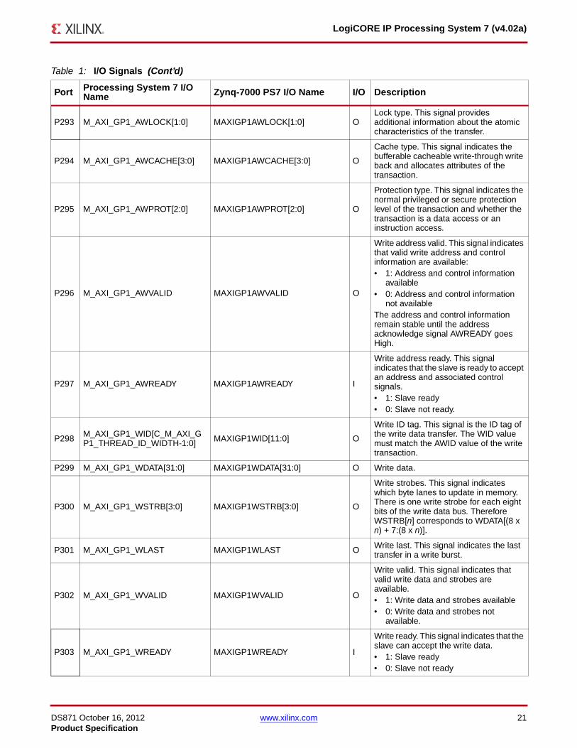
P293 M_AXI_GP1_AWLOCK[1:0] MAXIGP1AWLOCK[1:0] OLock type. This signal provides additional information about the atomic characteristics of the transfer.
P294 M_AXI_GP1_AWCACHE[3:0] MAXIGP1AWCACHE[3:0] O
Cache type. This signal indicates the bufferable cacheable write-through write back and allocates attributes of the transaction.
P295 M_AXI_GP1_AWPROT[2:0] MAXIGP1AWPROT[2:0] O
Protection type. This signal indicates the normal privileged or secure protection level of the transaction and whether the transaction is a data access or an instruction access.
P296 M_AXI_GP1_AWVALID MAXIGP1AWVALID O
Write address valid. This signal indicates that valid write address and control information are available:• 1: Address and control information
available• 0: Address and control information
not availableThe address and control information remain stable until the address acknowledge signal AWREADY goes High.
P297 M_AXI_GP1_AWREADY MAXIGP1AWREADY I
Write address ready. This signal indicates that the slave is ready to accept an address and associated control signals.• 1: Slave ready• 0: Slave not ready.
P298 M_AXI_GP1_WID[C_M_AXI_GP1_THREAD_ID_WIDTH-1:0] MAXIGP1WID[11:0] O
Write ID tag. This signal is the ID tag of the write data transfer. The WID value must match the AWID value of the write transaction.
P299 M_AXI_GP1_WDATA[31:0] MAXIGP1WDATA[31:0] O Write data.
P300 M_AXI_GP1_WSTRB[3:0] MAXIGP1WSTRB[3:0] O
Write strobes. This signal indicates which byte lanes to update in memory. There is one write strobe for each eight bits of the write data bus. Therefore WSTRB[n] corresponds to WDATA[(8 x n) + 7:(8 x n)].
P301 M_AXI_GP1_WLAST MAXIGP1WLAST O Write last. This signal indicates the last transfer in a write burst.
P302 M_AXI_GP1_WVALID MAXIGP1WVALID O
Write valid. This signal indicates that valid write data and strobes are available.• 1: Write data and strobes available• 0: Write data and strobes not
available.
P303 M_AXI_GP1_WREADY MAXIGP1WREADY I
Write ready. This signal indicates that the slave can accept the write data.• 1: Slave ready• 0: Slave not ready
Table 1: I/O Signals (Cont’d)
Port Processing System 7 I/O Name Zynq-7000 PS7 I/O Name I/O Description
DS871 October 16, 2012 www.xilinx.com 22Product Specification
LogiCORE IP Processing System 7 (v4.02a)
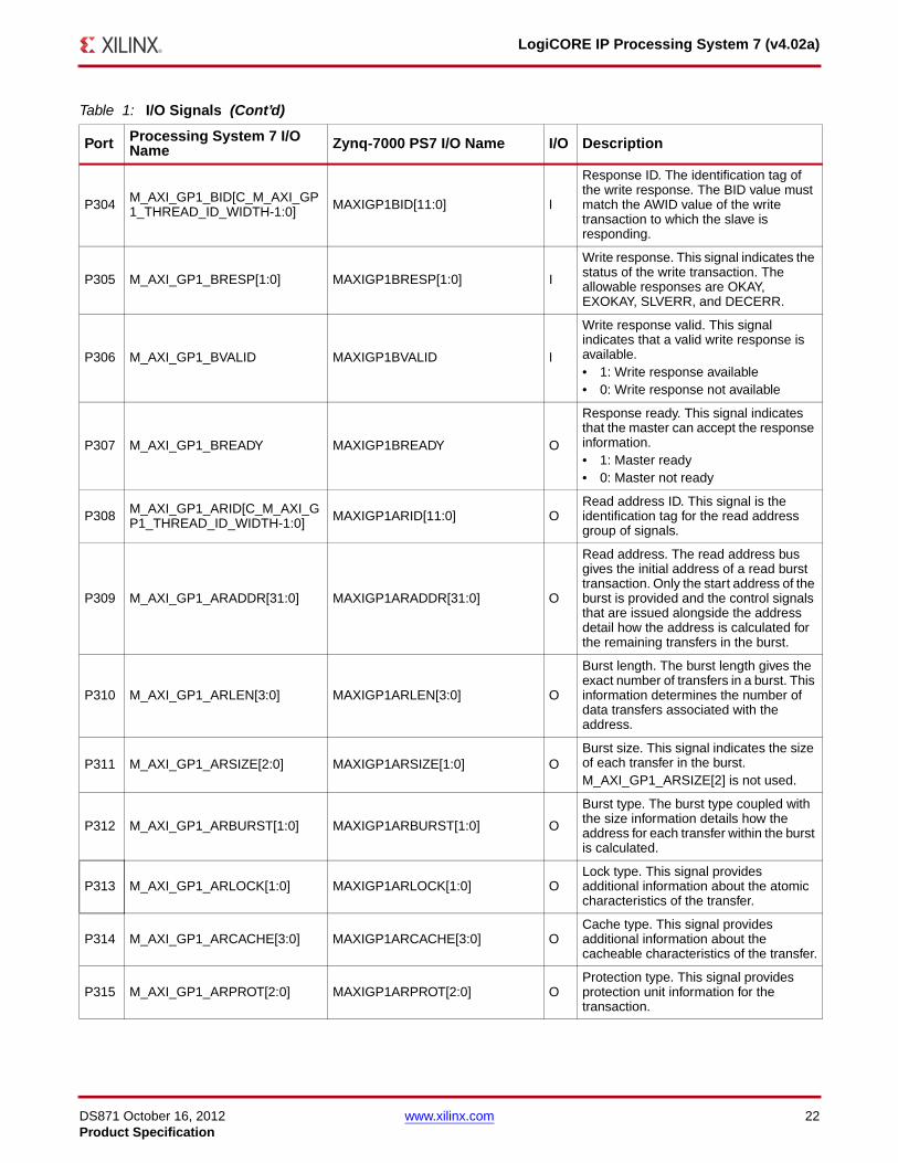
P304 M_AXI_GP1_BID[C_M_AXI_GP1_THREAD_ID_WIDTH-1:0] MAXIGP1BID[11:0] I
Response ID. The identification tag of the write response. The BID value must match the AWID value of the write transaction to which the slave is responding.
P305 M_AXI_GP1_BRESP[1:0] MAXIGP1BRESP[1:0] I
Write response. This signal indicates the status of the write transaction. The allowable responses are OKAY, EXOKAY, SLVERR, and DECERR.
P306 M_AXI_GP1_BVALID MAXIGP1BVALID I
Write response valid. This signal indicates that a valid write response is available.• 1: Write response available• 0: Write response not available
P307 M_AXI_GP1_BREADY MAXIGP1BREADY O
Response ready. This signal indicates that the master can accept the response information.• 1: Master ready• 0: Master not ready
P308 M_AXI_GP1_ARID[C_M_AXI_GP1_THREAD_ID_WIDTH-1:0] MAXIGP1ARID[11:0] O
Read address ID. This signal is the identification tag for the read address group of signals.
P309 M_AXI_GP1_ARADDR[31:0] MAXIGP1ARADDR[31:0] O
Read address. The read address bus gives the initial address of a read burst transaction. Only the start address of the burst is provided and the control signals that are issued alongside the address detail how the address is calculated for the remaining transfers in the burst.
P310 M_AXI_GP1_ARLEN[3:0] MAXIGP1ARLEN[3:0] O
Burst length. The burst length gives the exact number of transfers in a burst. This information determines the number of data transfers associated with the address.
P311 M_AXI_GP1_ARSIZE[2:0] MAXIGP1ARSIZE[1:0] OBurst size. This signal indicates the size of each transfer in the burst. M_AXI_GP1_ARSIZE[2] is not used.
P312 M_AXI_GP1_ARBURST[1:0] MAXIGP1ARBURST[1:0] O
Burst type. The burst type coupled with the size information details how the address for each transfer within the burst is calculated.
P313 M_AXI_GP1_ARLOCK[1:0] MAXIGP1ARLOCK[1:0] OLock type. This signal provides additional information about the atomic characteristics of the transfer.
P314 M_AXI_GP1_ARCACHE[3:0] MAXIGP1ARCACHE[3:0] OCache type. This signal provides additional information about the cacheable characteristics of the transfer.
P315 M_AXI_GP1_ARPROT[2:0] MAXIGP1ARPROT[2:0] OProtection type. This signal provides protection unit information for the transaction.
Table 1: I/O Signals (Cont’d)
Port Processing System 7 I/O Name Zynq-7000 PS7 I/O Name I/O Description
DS871 October 16, 2012 www.xilinx.com 23Product Specification
LogiCORE IP Processing System 7 (v4.02a)
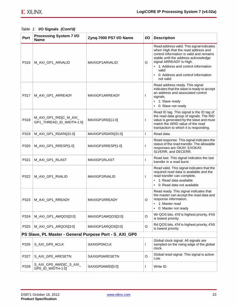
P316 M_AXI_GP1_ARVALID MAXIGP1ARVALID O
Read address valid. This signal indicates when High that the read address and control information is valid and remains stable until the address acknowledge signal ARREADY is High.• 1: Address and control information
valid• 0: Address and control information
not valid
P317 M_AXI_GP1_ARREADY MAXIGP1ARREADY I
Read address ready. This signal indicates that the slave is ready to accept an address and associated control signals.• 1: Slave ready• 0: Slave not ready
P318M_AXI_GP1_RID[C_M_AXI_GP1_THREAD_ID_WIDTH-1:0]
MAXIGP1RID[11:0] I
Read ID tag. This signal is the ID tag of the read data group of signals. The RID value is generated by the slave and must match the ARID value of the read transaction to which it is responding.
P319 M_AXI_GP1_RDATA[31:0] MAXIGP1RDATA[31:0] I Read data.
P320 M_AXI_GP1_RRESP[1:0] MAXIGP1RRESP[1:0] I
Read response. This signal indicates the status of the read transfer. The allowable responses are OKAY, EXOKAY, SLVERR, and DECERR.
P321 M_AXI_GP1_RLAST MAXIGP1RLAST I Read last. This signal indicates the last transfer in a read burst.
P322 M_AXI_GP1_RVALID MAXIGP1RVALID I
Read valid. This signal indicates that the required read data is available and the read transfer can complete.• 1: Read data available• 0: Read data not available
P323 M_AXI_GP1_RREADY MAXIGP1RREADY O
Read ready. This signal indicates that the master can accept the read data and response information.• 1: Master read• 0: Master not ready
P324 M_AXI_GP1_AWQOS[3:0] MAXIGP1AWQOS[3:0] O Wr QOS bits. 4'hf is highest priority, 4'h0 is lowest priority.
P325 M_AXI_GP1_ARQOS[3:0] MAXIGP1ARQOS[3:0] O Rd QOS bits. 4'hf is highest priority, 4'h0 is lowest priority.
PS Slave, PL Master - General Purpose Port - S_AXI_GP0
P326 S_AXI_GP0_ACLK SAXIGP0ACLK IGlobal clock signal. All signals are sampled on the rising edge of the global clock.
P327 S_AXI_GP0_ARESETN SAXIGP0ARESETN O Global reset signal. This signal is active- Low.
P328 S_AXI_GP0_AWID[C_S_AXI_GP0_ID_WIDTH-1:0] SAXIGP0AWID[5:0] I Write ID.
Table 1: I/O Signals (Cont’d)
Port Processing System 7 I/O Name Zynq-7000 PS7 I/O Name I/O Description
DS871 October 16, 2012 www.xilinx.com 24Product Specification
LogiCORE IP Processing System 7 (v4.02a)
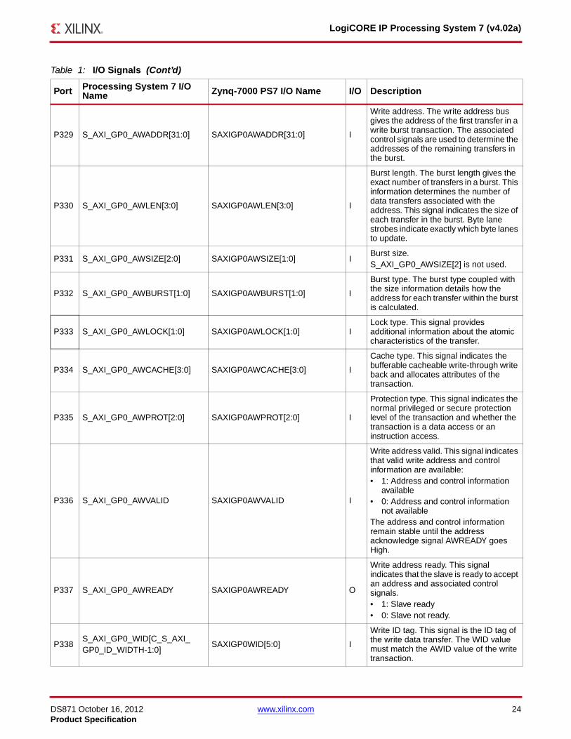
P329 S_AXI_GP0_AWADDR[31:0] SAXIGP0AWADDR[31:0] I
Write address. The write address bus gives the address of the first transfer in a write burst transaction. The associated control signals are used to determine the addresses of the remaining transfers in the burst.
P330 S_AXI_GP0_AWLEN[3:0] SAXIGP0AWLEN[3:0] I
Burst length. The burst length gives the exact number of transfers in a burst. This information determines the number of data transfers associated with the address. This signal indicates the size of each transfer in the burst. Byte lane strobes indicate exactly which byte lanes to update.
P331 S_AXI_GP0_AWSIZE[2:0] SAXIGP0AWSIZE[1:0] IBurst size.S_AXI_GP0_AWSIZE[2] is not used.
P332 S_AXI_GP0_AWBURST[1:0] SAXIGP0AWBURST[1:0] I
Burst type. The burst type coupled with the size information details how the address for each transfer within the burst is calculated.
P333 S_AXI_GP0_AWLOCK[1:0] SAXIGP0AWLOCK[1:0] ILock type. This signal provides additional information about the atomic characteristics of the transfer.
P334 S_AXI_GP0_AWCACHE[3:0] SAXIGP0AWCACHE[3:0] I
Cache type. This signal indicates the bufferable cacheable write-through write back and allocates attributes of the transaction.
P335 S_AXI_GP0_AWPROT[2:0] SAXIGP0AWPROT[2:0] I
Protection type. This signal indicates the normal privileged or secure protection level of the transaction and whether the transaction is a data access or an instruction access.
P336 S_AXI_GP0_AWVALID SAXIGP0AWVALID I
Write address valid. This signal indicates that valid write address and control information are available:• 1: Address and control information
available• 0: Address and control information
not availableThe address and control information remain stable until the address acknowledge signal AWREADY goes High.
P337 S_AXI_GP0_AWREADY SAXIGP0AWREADY O
Write address ready. This signal indicates that the slave is ready to accept an address and associated control signals.• 1: Slave ready• 0: Slave not ready.
P338S_AXI_GP0_WID[C_S_AXI_GP0_ID_WIDTH-1:0]
SAXIGP0WID[5:0] I
Write ID tag. This signal is the ID tag of the write data transfer. The WID value must match the AWID value of the write transaction.
Table 1: I/O Signals (Cont’d)
Port Processing System 7 I/O Name Zynq-7000 PS7 I/O Name I/O Description
DS871 October 16, 2012 www.xilinx.com 25Product Specification
LogiCORE IP Processing System 7 (v4.02a)
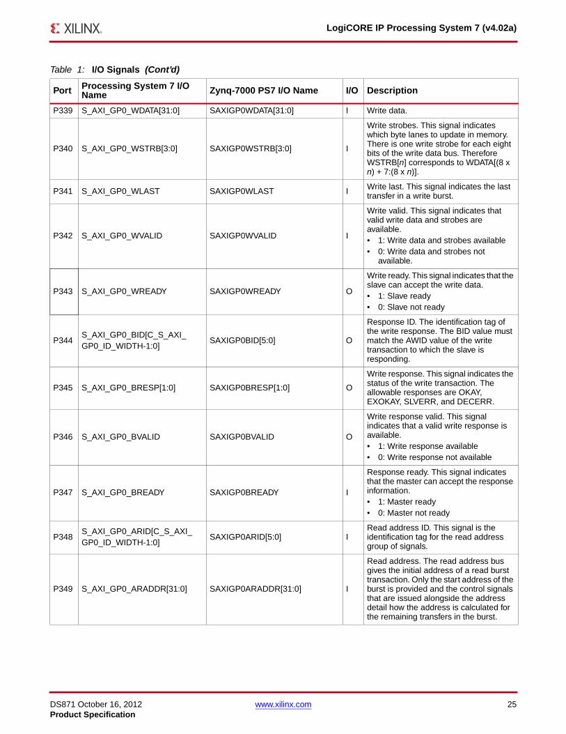
P339 S_AXI_GP0_WDATA[31:0] SAXIGP0WDATA[31:0] I Write data.
P340 S_AXI_GP0_WSTRB[3:0] SAXIGP0WSTRB[3:0] I
Write strobes. This signal indicates which byte lanes to update in memory. There is one write strobe for each eight bits of the write data bus. Therefore WSTRB[n] corresponds to WDATA[(8 x n) + 7:(8 x n)].
P341 S_AXI_GP0_WLAST SAXIGP0WLAST I Write last. This signal indicates the last transfer in a write burst.
P342 S_AXI_GP0_WVALID SAXIGP0WVALID I
Write valid. This signal indicates that valid write data and strobes are available.• 1: Write data and strobes available• 0: Write data and strobes not
available.
P343 S_AXI_GP0_WREADY SAXIGP0WREADY O
Write ready. This signal indicates that the slave can accept the write data.• 1: Slave ready• 0: Slave not ready
P344S_AXI_GP0_BID[C_S_AXI_GP0_ID_WIDTH-1:0]
SAXIGP0BID[5:0] O
Response ID. The identification tag of the write response. The BID value must match the AWID value of the write transaction to which the slave is responding.
P345 S_AXI_GP0_BRESP[1:0] SAXIGP0BRESP[1:0] O
Write response. This signal indicates the status of the write transaction. The allowable responses are OKAY, EXOKAY, SLVERR, and DECERR.
P346 S_AXI_GP0_BVALID SAXIGP0BVALID O
Write response valid. This signal indicates that a valid write response is available.• 1: Write response available• 0: Write response not available
P347 S_AXI_GP0_BREADY SAXIGP0BREADY I
Response ready. This signal indicates that the master can accept the response information.• 1: Master ready• 0: Master not ready
P348S_AXI_GP0_ARID[C_S_AXI_GP0_ID_WIDTH-1:0]
SAXIGP0ARID[5:0] IRead address ID. This signal is the identification tag for the read address group of signals.
P349 S_AXI_GP0_ARADDR[31:0] SAXIGP0ARADDR[31:0] I
Read address. The read address bus gives the initial address of a read burst transaction. Only the start address of the burst is provided and the control signals that are issued alongside the address detail how the address is calculated for the remaining transfers in the burst.
Table 1: I/O Signals (Cont’d)
Port Processing System 7 I/O Name Zynq-7000 PS7 I/O Name I/O Description
DS871 October 16, 2012 www.xilinx.com 26Product Specification
LogiCORE IP Processing System 7 (v4.02a)
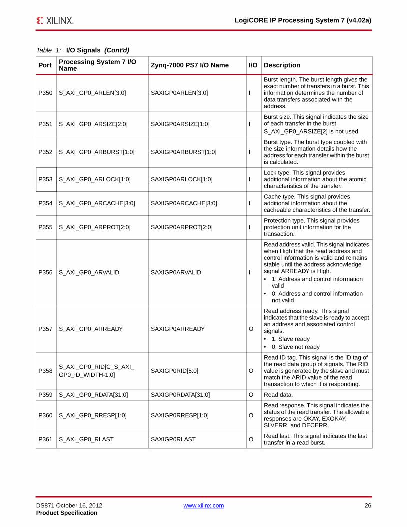
P350 S_AXI_GP0_ARLEN[3:0] SAXIGP0ARLEN[3:0] I
Burst length. The burst length gives the exact number of transfers in a burst. This information determines the number of data transfers associated with the address.
P351 S_AXI_GP0_ARSIZE[2:0] SAXIGP0ARSIZE[1:0] IBurst size. This signal indicates the size of each transfer in the burst. S_AXI_GP0_ARSIZE[2] is not used.
P352 S_AXI_GP0_ARBURST[1:0] SAXIGP0ARBURST[1:0] I
Burst type. The burst type coupled with the size information details how the address for each transfer within the burst is calculated.
P353 S_AXI_GP0_ARLOCK[1:0] SAXIGP0ARLOCK[1:0] ILock type. This signal provides additional information about the atomic characteristics of the transfer.
P354 S_AXI_GP0_ARCACHE[3:0] SAXIGP0ARCACHE[3:0] ICache type. This signal provides additional information about the cacheable characteristics of the transfer.
P355 S_AXI_GP0_ARPROT[2:0] SAXIGP0ARPROT[2:0] IProtection type. This signal provides protection unit information for the transaction.
P356 S_AXI_GP0_ARVALID SAXIGP0ARVALID I
Read address valid. This signal indicates when High that the read address and control information is valid and remains stable until the address acknowledge signal ARREADY is High.• 1: Address and control information
valid• 0: Address and control information
not valid
P357 S_AXI_GP0_ARREADY SAXIGP0ARREADY O
Read address ready. This signal indicates that the slave is ready to accept an address and associated control signals.• 1: Slave ready• 0: Slave not ready
P358S_AXI_GP0_RID[C_S_AXI_GP0_ID_WIDTH-1:0]
SAXIGP0RID[5:0] O
Read ID tag. This signal is the ID tag of the read data group of signals. The RID value is generated by the slave and must match the ARID value of the read transaction to which it is responding.
P359 S_AXI_GP0_RDATA[31:0] SAXIGP0RDATA[31:0] O Read data.
P360 S_AXI_GP0_RRESP[1:0] SAXIGP0RRESP[1:0] O
Read response. This signal indicates the status of the read transfer. The allowable responses are OKAY, EXOKAY, SLVERR, and DECERR.
P361 S_AXI_GP0_RLAST SAXIGP0RLAST O Read last. This signal indicates the last transfer in a read burst.
Table 1: I/O Signals (Cont’d)
Port Processing System 7 I/O Name Zynq-7000 PS7 I/O Name I/O Description
DS871 October 16, 2012 www.xilinx.com 27Product Specification
LogiCORE IP Processing System 7 (v4.02a)
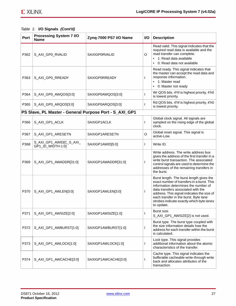
P362 S_AXI_GP0_RVALID SAXIGP0RVALID O
Read valid. This signal indicates that the required read data is available and the read transfer can complete.• 1: Read data available• 0: Read data not available
P363 S_AXI_GP0_RREADY SAXIGP0RREADY I
Read ready. This signal indicates that the master can accept the read data and response information.• 1: Master read• 0: Master not ready
P364 S_AXI_GP0_AWQOS[3:0] SAXIGP0AWQOS[3:0] I Wr QOS bits. 4'hf is highest priority, 4'h0 is lowest priority.
P365 S_AXI_GP0_ARQOS[3:0] SAXIGP0ARQOS[3:0] I Rd QOS bits. 4'hf is highest priority, 4'h0 is lowest priority.
PS Slave, PL Master - General Purpose Port - S_AXI_GP1
P366 S_AXI_GP1_ACLK SAXIGP1ACLK IGlobal clock signal. All signals are sampled on the rising edge of the global clock.
P367 S_AXI_GP1_ARESETN SAXIGP1ARESETN O Global reset signal. This signal is active-Low.
P368 S_AXI_GP1_AWID[C_S_AXI_GP1_ID_WIDTH-1:0] SAXIGP1AWID[5:0] I Write ID.
P369 S_AXI_GP1_AWADDR[31:0] SAXIGP1AWADDR[31:0] I
Write address. The write address bus gives the address of the first transfer in a write burst transaction. The associated control signals are used to determine the addresses of the remaining transfers in the burst.
P370 S_AXI_GP1_AWLEN[3:0] SAXIGP1AWLEN[3:0] I
Burst length. The burst length gives the exact number of transfers in a burst. This information determines the number of data transfers associated with the address. This signal indicates the size of each transfer in the burst. Byte lane strobes indicate exactly which byte lanes to update.
P371 S_AXI_GP1_AWSIZE[2:0] SAXIGP1AWSIZE[1:0] IBurst size.S_AXI_GP1_AWSIZE[2] is not used.
P372 S_AXI_GP1_AWBURST[1:0] SAXIGP1AWBURST[1:0] I
Burst type. The burst type coupled with the size information details how the address for each transfer within the burst is calculated.
P373 S_AXI_GP1_AWLOCK[1:0] SAXIGP1AWLOCK[1:0] ILock type. This signal provides additional information about the atomic characteristics of the transfer.
P374 S_AXI_GP1_AWCACHE[3:0] SAXIGP1AWCACHE[3:0] I
Cache type. This signal indicates the bufferable cacheable write-through write back and allocates attributes of the transaction.
Table 1: I/O Signals (Cont’d)
Port Processing System 7 I/O Name Zynq-7000 PS7 I/O Name I/O Description
DS871 October 16, 2012 www.xilinx.com 28Product Specification
LogiCORE IP Processing System 7 (v4.02a)
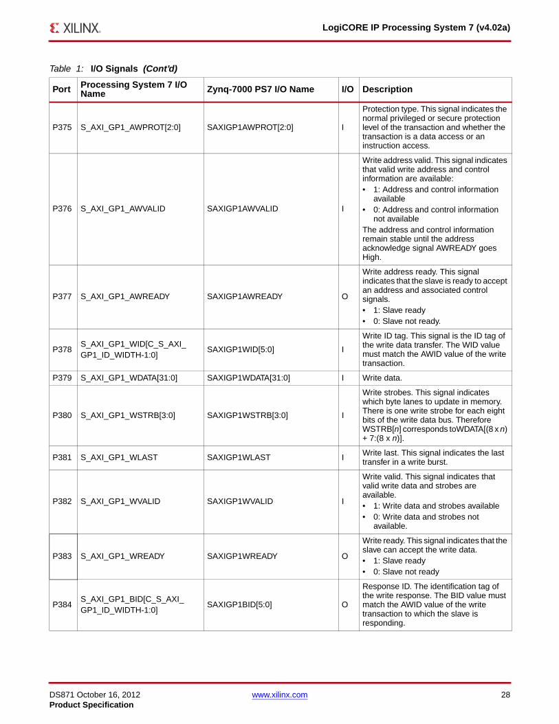
P375 S_AXI_GP1_AWPROT[2:0] SAXIGP1AWPROT[2:0] I
Protection type. This signal indicates the normal privileged or secure protection level of the transaction and whether the transaction is a data access or an instruction access.
P376 S_AXI_GP1_AWVALID SAXIGP1AWVALID I
Write address valid. This signal indicates that valid write address and control information are available:• 1: Address and control information
available• 0: Address and control information
not availableThe address and control information remain stable until the address acknowledge signal AWREADY goes High.
P377 S_AXI_GP1_AWREADY SAXIGP1AWREADY O
Write address ready. This signal indicates that the slave is ready to accept an address and associated control signals.• 1: Slave ready• 0: Slave not ready.
P378S_AXI_GP1_WID[C_S_AXI_GP1_ID_WIDTH-1:0]
SAXIGP1WID[5:0] I
Write ID tag. This signal is the ID tag of the write data transfer. The WID value must match the AWID value of the write transaction.
P379 S_AXI_GP1_WDATA[31:0] SAXIGP1WDATA[31:0] I Write data.
P380 S_AXI_GP1_WSTRB[3:0] SAXIGP1WSTRB[3:0] I
Write strobes. This signal indicates which byte lanes to update in memory. There is one write strobe for each eight bits of the write data bus. Therefore WSTRB[n] corresponds toWDATA[(8 x n) + 7:(8 x n)].
P381 S_AXI_GP1_WLAST SAXIGP1WLAST I Write last. This signal indicates the last transfer in a write burst.
P382 S_AXI_GP1_WVALID SAXIGP1WVALID I
Write valid. This signal indicates that valid write data and strobes are available.• 1: Write data and strobes available• 0: Write data and strobes not
available.
P383 S_AXI_GP1_WREADY SAXIGP1WREADY O
Write ready. This signal indicates that the slave can accept the write data.• 1: Slave ready• 0: Slave not ready
P384S_AXI_GP1_BID[C_S_AXI_GP1_ID_WIDTH-1:0]
SAXIGP1BID[5:0] O
Response ID. The identification tag of the write response. The BID value must match the AWID value of the write transaction to which the slave is responding.
Table 1: I/O Signals (Cont’d)
Port Processing System 7 I/O Name Zynq-7000 PS7 I/O Name I/O Description
DS871 October 16, 2012 www.xilinx.com 29Product Specification
LogiCORE IP Processing System 7 (v4.02a)
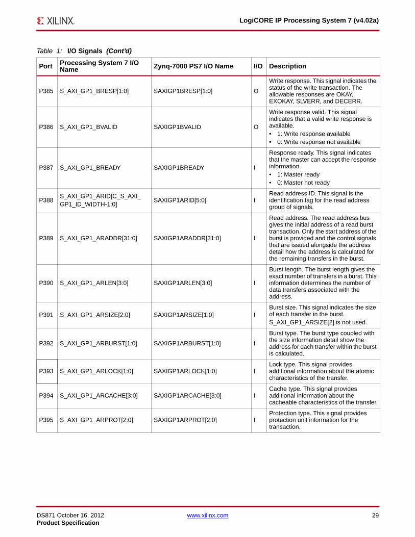
P385 S_AXI_GP1_BRESP[1:0] SAXIGP1BRESP[1:0] O
Write response. This signal indicates the status of the write transaction. The allowable responses are OKAY, EXOKAY, SLVERR, and DECERR.
P386 S_AXI_GP1_BVALID SAXIGP1BVALID O
Write response valid. This signal indicates that a valid write response is available.• 1: Write response available• 0: Write response not available
P387 S_AXI_GP1_BREADY SAXIGP1BREADY I
Response ready. This signal indicates that the master can accept the response information.• 1: Master ready• 0: Master not ready
P388S_AXI_GP1_ARID[C_S_AXI_GP1_ID_WIDTH-1:0]
SAXIGP1ARID[5:0] IRead address ID. This signal is the identification tag for the read address group of signals.
P389 S_AXI_GP1_ARADDR[31:0] SAXIGP1ARADDR[31:0] I
Read address. The read address bus gives the initial address of a read burst transaction. Only the start address of the burst is provided and the control signals that are issued alongside the address detail how the address is calculated for the remaining transfers in the burst.
P390 S_AXI_GP1_ARLEN[3:0] SAXIGP1ARLEN[3:0] I
Burst length. The burst length gives the exact number of transfers in a burst. This information determines the number of data transfers associated with the address.
P391 S_AXI_GP1_ARSIZE[2:0] SAXIGP1ARSIZE[1:0] IBurst size. This signal indicates the size of each transfer in the burst. S_AXI_GP1_ARSIZE[2] is not used.
P392 S_AXI_GP1_ARBURST[1:0] SAXIGP1ARBURST[1:0] I
Burst type. The burst type coupled with the size information detail show the address for each transfer within the burst is calculated.
P393 S_AXI_GP1_ARLOCK[1:0] SAXIGP1ARLOCK[1:0] ILock type. This signal provides additional information about the atomic characteristics of the transfer.
P394 S_AXI_GP1_ARCACHE[3:0] SAXIGP1ARCACHE[3:0] ICache type. This signal provides additional information about the cacheable characteristics of the transfer.
P395 S_AXI_GP1_ARPROT[2:0] SAXIGP1ARPROT[2:0] IProtection type. This signal provides protection unit information for the transaction.
Table 1: I/O Signals (Cont’d)
Port Processing System 7 I/O Name Zynq-7000 PS7 I/O Name I/O Description
DS871 October 16, 2012 www.xilinx.com 30Product Specification
LogiCORE IP Processing System 7 (v4.02a)
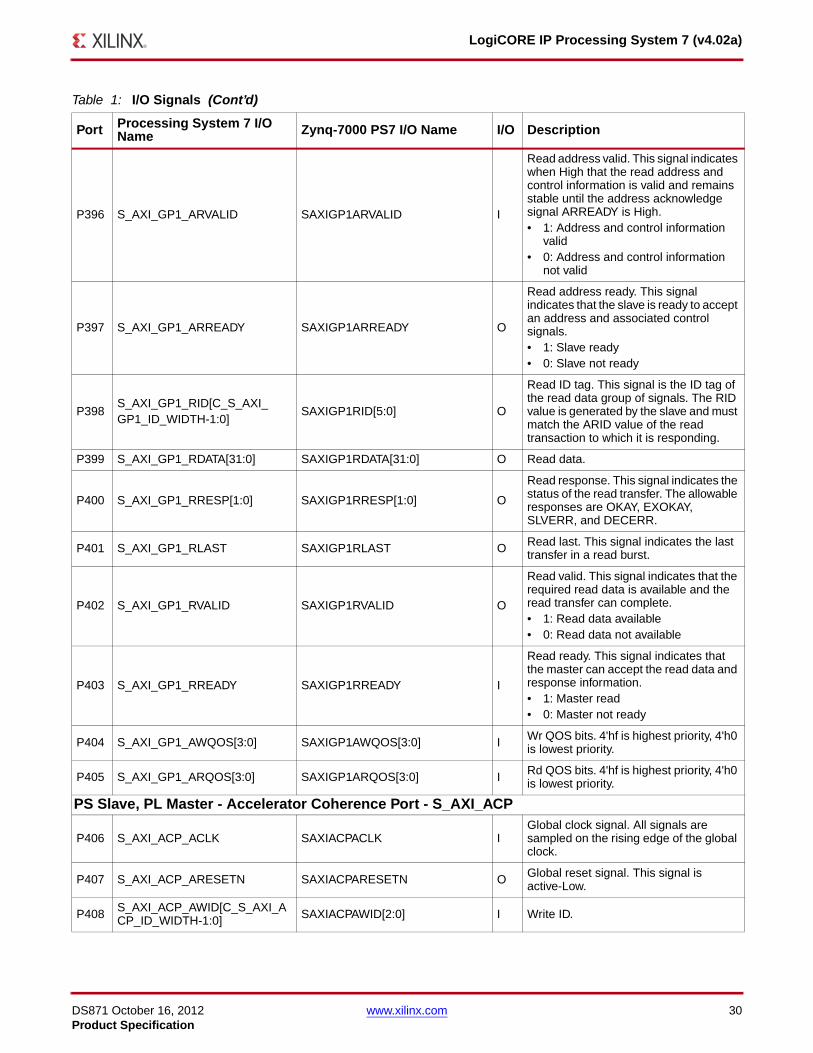
P396 S_AXI_GP1_ARVALID SAXIGP1ARVALID I
Read address valid. This signal indicates when High that the read address and control information is valid and remains stable until the address acknowledge signal ARREADY is High.• 1: Address and control information
valid• 0: Address and control information
not valid
P397 S_AXI_GP1_ARREADY SAXIGP1ARREADY O
Read address ready. This signal indicates that the slave is ready to accept an address and associated control signals.• 1: Slave ready• 0: Slave not ready
P398S_AXI_GP1_RID[C_S_AXI_GP1_ID_WIDTH-1:0]
SAXIGP1RID[5:0] O
Read ID tag. This signal is the ID tag of the read data group of signals. The RID value is generated by the slave and must match the ARID value of the read transaction to which it is responding.
P399 S_AXI_GP1_RDATA[31:0] SAXIGP1RDATA[31:0] O Read data.
P400 S_AXI_GP1_RRESP[1:0] SAXIGP1RRESP[1:0] O
Read response. This signal indicates the status of the read transfer. The allowable responses are OKAY, EXOKAY, SLVERR, and DECERR.
P401 S_AXI_GP1_RLAST SAXIGP1RLAST O Read last. This signal indicates the last transfer in a read burst.
P402 S_AXI_GP1_RVALID SAXIGP1RVALID O
Read valid. This signal indicates that the required read data is available and the read transfer can complete.• 1: Read data available• 0: Read data not available
P403 S_AXI_GP1_RREADY SAXIGP1RREADY I
Read ready. This signal indicates that the master can accept the read data and response information.• 1: Master read• 0: Master not ready
P404 S_AXI_GP1_AWQOS[3:0] SAXIGP1AWQOS[3:0] I Wr QOS bits. 4'hf is highest priority, 4'h0 is lowest priority.
P405 S_AXI_GP1_ARQOS[3:0] SAXIGP1ARQOS[3:0] I Rd QOS bits. 4'hf is highest priority, 4'h0 is lowest priority.
PS Slave, PL Master - Accelerator Coherence Port - S_AXI_ACP
P406 S_AXI_ACP_ACLK SAXIACPACLK IGlobal clock signal. All signals are sampled on the rising edge of the global clock.
P407 S_AXI_ACP_ARESETN SAXIACPARESETN O Global reset signal. This signal is active-Low.
P408 S_AXI_ACP_AWID[C_S_AXI_ACP_ID_WIDTH-1:0] SAXIACPAWID[2:0] I Write ID.
Table 1: I/O Signals (Cont’d)
Port Processing System 7 I/O Name Zynq-7000 PS7 I/O Name I/O Description

DS871 October 16, 2012 www.xilinx.com 31Product Specification
LogiCORE IP Processing System 7 (v4.02a)
P409 S_AXI_ACP_AWADDR[31:0] SAXIACPAWADDR[31:0] I
Write address. The write address bus gives the address of the first transfer in a write burst transaction. The associated control signals are used to determine the addresses of the remaining transfers in the burst.
P410 S_AXI_ACP_AWLEN[3:0] SAXIACPAWLEN[3:0] I
Burst length. The burst length gives the exact number of transfers in a burst. This information determines the number of data transfers associated with the address. This signal indicates the size of each transfer in the burst. Byte lane strobes indicate exactly which byte lanes to update.
P411 S_AXI_ACP_AWSIZE[2:0] SAXIACPAWSIZE[1:0] IBurst size.S_AXI_ACP_AWSIZE[2] is not used.
P412 S_AXI_ACP_AWBURST[1:0] SAXIACPAWBURST[1:0] I
Burst type. The burst type coupled with the size information details how the address for each transfer within the burst is calculated.
P413 S_AXI_ACP_AWLOCK[1:0] SAXIACPAWLOCK[1:0] ILock type. This signal provides additional information about the atomic characteristics of the transfer.
P414 S_AXI_ACP_AWCACHE[3:0] SAXIACPAWCACHE[3:0] I
Cache type. This signal indicates the bufferable cacheable write-through write back and allocates attributes of the transaction.
P415 S_AXI_ACP_AWPROT[2:0] SAXIACPAWPROT[2:0] I
Protection type. This signal indicates the normal privileged or secure protection level of the transaction and whether the transaction is a data access or an instruction access.
P416 S_AXI_ACP_AWVALID SAXIACPAWVALID I
Write address valid. This signal indicates that valid write address and control information are available:• 1: Address and control information
available• 0: Address and control information
not availableThe address and control information remain stable until the address acknowledge signal AWREADY goes High.
P417 S_AXI_ACP_AWREADY SAXIACPAWREADY O
Write address ready. This signal indicates that the slave is ready to accept an address and associated control signals.• 1: Slave ready• 0: Slave not ready.
P418S_AXI_ACP_WID[C_S_AXI_ACP_ID_WIDTH-1:0]
SAXIACPWID[2:0] I
Write ID tag. This signal is the ID tag of the write data transfer. The WID value must match the AWID value of the write transaction.
Table 1: I/O Signals (Cont’d)
Port Processing System 7 I/O Name Zynq-7000 PS7 I/O Name I/O Description

DS871 October 16, 2012 www.xilinx.com 32Product Specification
LogiCORE IP Processing System 7 (v4.02a)
P419 S_AXI_ACP_WDATA[63:0] SAXIACPWDATA[63:0] I Write data.
P420 S_AXI_ACP_WSTRB[7:0] SAXIACPWSTRB[7:0] I
Write strobes. This signal indicates which byte lanes to update in memory. There is one write strobe for each eight bits of the write data bus. Therefore WSTRB[n] corresponds toWDATA[(8 x n) + 7:(8 x n)].
P421 S_AXI_ACP_WLAST SAXIACPWLAST I Write last. This signal indicates the last transfer in a write burst.
P422 S_AXI_ACP_WVALID SAXIACPWVALID I
Write valid. This signal indicates that valid write data and strobes are available.• 1: Write data and strobes available• 0: Write data and strobes not
available.
P423 S_AXI_ACP_WREADY SAXIACPWREADY O
Write ready. This signal indicates that the slave can accept the write data.• 1: Slave ready• 0: Slave not ready
P424S_AXI_ACP_BID[C_S_AXI_ACP_ID_WIDTH-1:0]
SAXIACPBID[2:0] O
Response ID. The identification tag of the write response. The BID value must match the AWID value of the write transaction to which the slave is responding.
P425 S_AXI_ACP_BRESP[1:0] SAXIACPBRESP[1:0] O
Write response. This signal indicates the status of the write transaction. The allowable responses are OKAY, EXOKAY, SLVERR, and DECERR.
P426 S_AXI_ACP_BVALID SAXIACPBVALID O
Write response valid. This signal indicates that a valid write response is available.• 1: Write response available• 0: Write response not available
P427 S_AXI_ACP_BREADY SAXIACPBREADY I
Response ready. This signal indicates that the master can accept the response information.• 1: Master ready• 0: Master not ready
P428S_AXI_ACP_ARID[C_S_AXI_ACP_ID_WIDTH-1:0]
SAXIACPARID[2:0] IRead address ID. This signal is the identification tag for the read address group of signals.
P429 S_AXI_ACP_ARADDR[31:0] SAXIACPARADDR[31:0] I
Read address. The read address bus gives the initial address of a read burst transaction. Only the start address of the burst is provided and the control signals that are issued alongside the address detail how the address is calculated for the remaining transfers in the burst.
Table 1: I/O Signals (Cont’d)
Port Processing System 7 I/O Name Zynq-7000 PS7 I/O Name I/O Description

DS871 October 16, 2012 www.xilinx.com 33Product Specification
LogiCORE IP Processing System 7 (v4.02a)
P430 S_AXI_ACP_ARLEN[3:0] SAXIACPARLEN[3:0] I
Burst length. The burst length gives the exact number of transfers in a burst. This information determines the number of data transfers associated with the address.
P431 S_AXI_ACP_ARSIZE[2:0] SAXIACPARSIZE[1:0] IBurst size. This signal indicates the size of each transfer in the burst. S_AXI_ACP_ARSIZE[2] is not used.
P432 S_AXI_ACP_ARBURST[1:0] SAXIACPARBURST[1:0] I
Burst type. The burst type coupled with the size information details how the address for each transfer within the burst is calculated.
P433 S_AXI_ACP_ARLOCK[1:0] SAXIACPARLOCK[1:0] ILock type. This signal provides additional information about the atomic characteristics of the transfer.
P434 S_AXI_ACP_ARCACHE[3:0] SAXIACPARCACHE[3:0] ICache type. This signal provides additional information about the cacheable characteristics of the transfer.
P435 S_AXI_ACP_ARPROT[2:0] SAXIACPARPROT[2:0] IProtection type. This signal provides protection unit information for the transaction.
P436 S_AXI_ACP_ARVALID SAXIACPARVALID I
Read address valid. This signal indicates when High that the read address and control information is valid and remains stable until the address acknowledge signal ARREADY is High.• 1: Address and control information
valid• 0: Address and control information
not valid
P437 S_AXI_ACP_ARREADY SAXIACPARREADY O
Read address ready. This signal indicates that the slave is ready to accept an address and associated control signals.• 1: Slave ready• 0: Slave not ready
P438S_AXI_ACP_RID[C_S_AXI_ACP_ID_WIDTH-1:0]
SAXIACPRID[2:0] O
Read ID tag. This signal is the ID tag of the read data group of signals. The RID value is generated by the slave and must match the ARID value of the read transaction to which it is responding.
P439 S_AXI_ACP_RDATA[63:0] SAXIACPRDATA[63:0] O Read data.
P440 S_AXI_ACP_RRESP[1:0] SAXIACPRRESP[1:0] O
Read response. This signal indicates the status of the read transfer. The allowable responses are OKAY, EXOKAY, SLVERR, and DECERR.
P441 S_AXI_ACP_RLAST SAXIACPRLAST O Read last. This signal indicates the last transfer in a read burst.
Table 1: I/O Signals (Cont’d)
Port Processing System 7 I/O Name Zynq-7000 PS7 I/O Name I/O Description
DS871 October 16, 2012 www.xilinx.com 34Product Specification
LogiCORE IP Processing System 7 (v4.02a)
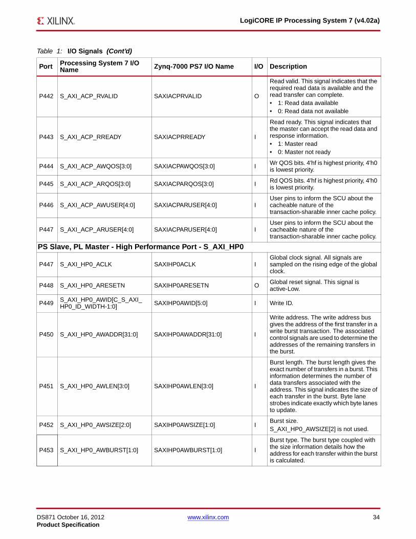
P442 S_AXI_ACP_RVALID SAXIACPRVALID O
Read valid. This signal indicates that the required read data is available and the read transfer can complete.• 1: Read data available• 0: Read data not available
P443 S_AXI_ACP_RREADY SAXIACPRREADY I
Read ready. This signal indicates that the master can accept the read data and response information.• 1: Master read• 0: Master not ready
P444 S_AXI_ACP_AWQOS[3:0] SAXIACPAWQOS[3:0] I Wr QOS bits. 4'hf is highest priority, 4'h0 is lowest priority.
P445 S_AXI_ACP_ARQOS[3:0] SAXIACPARQOS[3:0] I Rd QOS bits. 4'hf is highest priority, 4'h0 is lowest priority.
P446 S_AXI_ACP_AWUSER[4:0] SAXIACPARUSER[4:0] IUser pins to inform the SCU about the cacheable nature of the transaction-sharable inner cache policy.
P447 S_AXI_ACP_ARUSER[4:0] SAXIACPARUSER[4:0] IUser pins to inform the SCU about the cacheable nature of the transaction-sharable inner cache policy.
PS Slave, PL Master - High Performance Port - S_AXI_HP0
P447 S_AXI_HP0_ACLK SAXIHP0ACLK IGlobal clock signal. All signals are sampled on the rising edge of the global clock.
P448 S_AXI_HP0_ARESETN SAXIHP0ARESETN O Global reset signal. This signal is active-Low.
P449 S_AXI_HP0_AWID[C_S_AXI_HP0_ID_WIDTH-1:0] SAXIHP0AWID[5:0] I Write ID.
P450 S_AXI_HP0_AWADDR[31:0] SAXIHP0AWADDR[31:0] I
Write address. The write address bus gives the address of the first transfer in a write burst transaction. The associated control signals are used to determine the addresses of the remaining transfers in the burst.
P451 S_AXI_HP0_AWLEN[3:0] SAXIHP0AWLEN[3:0] I
Burst length. The burst length gives the exact number of transfers in a burst. This information determines the number of data transfers associated with the address. This signal indicates the size of each transfer in the burst. Byte lane strobes indicate exactly which byte lanes to update.
P452 S_AXI_HP0_AWSIZE[2:0] SAXIHP0AWSIZE[1:0] IBurst size.S_AXI_HP0_AWSIZE[2] is not used.
P453 S_AXI_HP0_AWBURST[1:0] SAXIHP0AWBURST[1:0] I
Burst type. The burst type coupled with the size information details how the address for each transfer within the burst is calculated.
Table 1: I/O Signals (Cont’d)
Port Processing System 7 I/O Name Zynq-7000 PS7 I/O Name I/O Description
DS871 October 16, 2012 www.xilinx.com 35Product Specification
LogiCORE IP Processing System 7 (v4.02a)
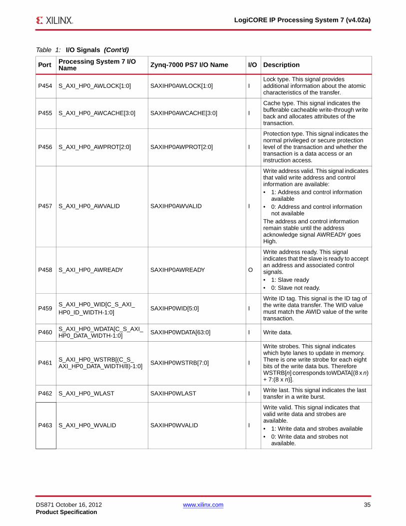
P454 S_AXI_HP0_AWLOCK[1:0] SAXIHP0AWLOCK[1:0] ILock type. This signal provides additional information about the atomic characteristics of the transfer.
P455 S_AXI_HP0_AWCACHE[3:0] SAXIHP0AWCACHE[3:0] I
Cache type. This signal indicates the bufferable cacheable write-through write back and allocates attributes of the transaction.
P456 S_AXI_HP0_AWPROT[2:0] SAXIHP0AWPROT[2:0] I
Protection type. This signal indicates the normal privileged or secure protection level of the transaction and whether the transaction is a data access or an instruction access.
P457 S_AXI_HP0_AWVALID SAXIHP0AWVALID I
Write address valid. This signal indicates that valid write address and control information are available:• 1: Address and control information
available• 0: Address and control information
not availableThe address and control information remain stable until the address acknowledge signal AWREADY goes High.
P458 S_AXI_HP0_AWREADY SAXIHP0AWREADY O
Write address ready. This signal indicates that the slave is ready to accept an address and associated control signals.• 1: Slave ready• 0: Slave not ready.
P459S_AXI_HP0_WID[C_S_AXI_HP0_ID_WIDTH-1:0]
SAXIHP0WID[5:0] I
Write ID tag. This signal is the ID tag of the write data transfer. The WID value must match the AWID value of the write transaction.
P460 S_AXI_HP0_WDATA[C_S_AXI_HP0_DATA_WIDTH-1:0] SAXIHP0WDATA[63:0] I Write data.
P461 S_AXI_HP0_WSTRB[(C_S_AXI_HP0_DATA_WIDTH/8)-1:0] SAXIHP0WSTRB[7:0] I
Write strobes. This signal indicates which byte lanes to update in memory. There is one write strobe for each eight bits of the write data bus. Therefore WSTRB[n] corresponds toWDATA[(8 x n) + 7:(8 x n)].
P462 S_AXI_HP0_WLAST SAXIHP0WLAST I Write last. This signal indicates the last transfer in a write burst.
P463 S_AXI_HP0_WVALID SAXIHP0WVALID I
Write valid. This signal indicates that valid write data and strobes are available.• 1: Write data and strobes available• 0: Write data and strobes not
available.
Table 1: I/O Signals (Cont’d)
Port Processing System 7 I/O Name Zynq-7000 PS7 I/O Name I/O Description
DS871 October 16, 2012 www.xilinx.com 36Product Specification
LogiCORE IP Processing System 7 (v4.02a)
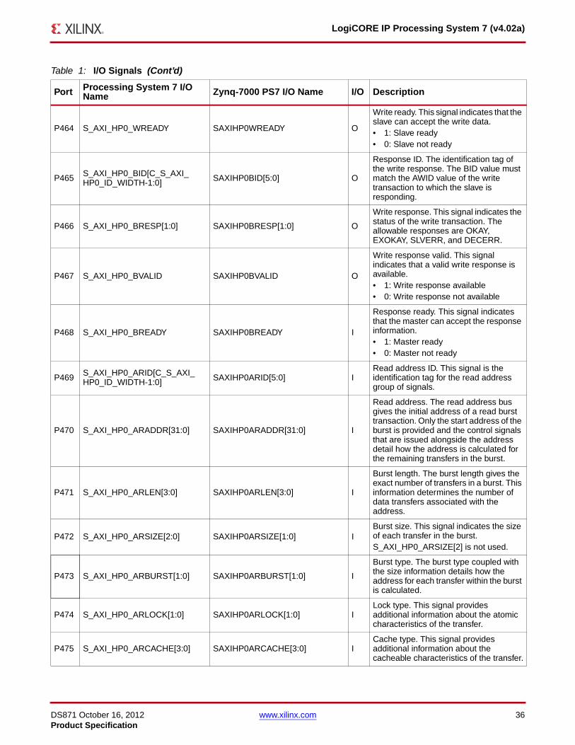
P464 S_AXI_HP0_WREADY SAXIHP0WREADY O
Write ready. This signal indicates that the slave can accept the write data.• 1: Slave ready• 0: Slave not ready
P465 S_AXI_HP0_BID[C_S_AXI_HP0_ID_WIDTH-1:0] SAXIHP0BID[5:0] O
Response ID. The identification tag of the write response. The BID value must match the AWID value of the write transaction to which the slave is responding.
P466 S_AXI_HP0_BRESP[1:0] SAXIHP0BRESP[1:0] O
Write response. This signal indicates the status of the write transaction. The allowable responses are OKAY, EXOKAY, SLVERR, and DECERR.
P467 S_AXI_HP0_BVALID SAXIHP0BVALID O
Write response valid. This signal indicates that a valid write response is available.• 1: Write response available• 0: Write response not available
P468 S_AXI_HP0_BREADY SAXIHP0BREADY I
Response ready. This signal indicates that the master can accept the response information.• 1: Master ready• 0: Master not ready
P469 S_AXI_HP0_ARID[C_S_AXI_HP0_ID_WIDTH-1:0] SAXIHP0ARID[5:0] I
Read address ID. This signal is the identification tag for the read address group of signals.
P470 S_AXI_HP0_ARADDR[31:0] SAXIHP0ARADDR[31:0] I
Read address. The read address bus gives the initial address of a read burst transaction. Only the start address of the burst is provided and the control signals that are issued alongside the address detail how the address is calculated for the remaining transfers in the burst.
P471 S_AXI_HP0_ARLEN[3:0] SAXIHP0ARLEN[3:0] I
Burst length. The burst length gives the exact number of transfers in a burst. This information determines the number of data transfers associated with the address.
P472 S_AXI_HP0_ARSIZE[2:0] SAXIHP0ARSIZE[1:0] IBurst size. This signal indicates the size of each transfer in the burst. S_AXI_HP0_ARSIZE[2] is not used.
P473 S_AXI_HP0_ARBURST[1:0] SAXIHP0ARBURST[1:0] I
Burst type. The burst type coupled with the size information details how the address for each transfer within the burst is calculated.
P474 S_AXI_HP0_ARLOCK[1:0] SAXIHP0ARLOCK[1:0] ILock type. This signal provides additional information about the atomic characteristics of the transfer.
P475 S_AXI_HP0_ARCACHE[3:0] SAXIHP0ARCACHE[3:0] ICache type. This signal provides additional information about the cacheable characteristics of the transfer.
Table 1: I/O Signals (Cont’d)
Port Processing System 7 I/O Name Zynq-7000 PS7 I/O Name I/O Description
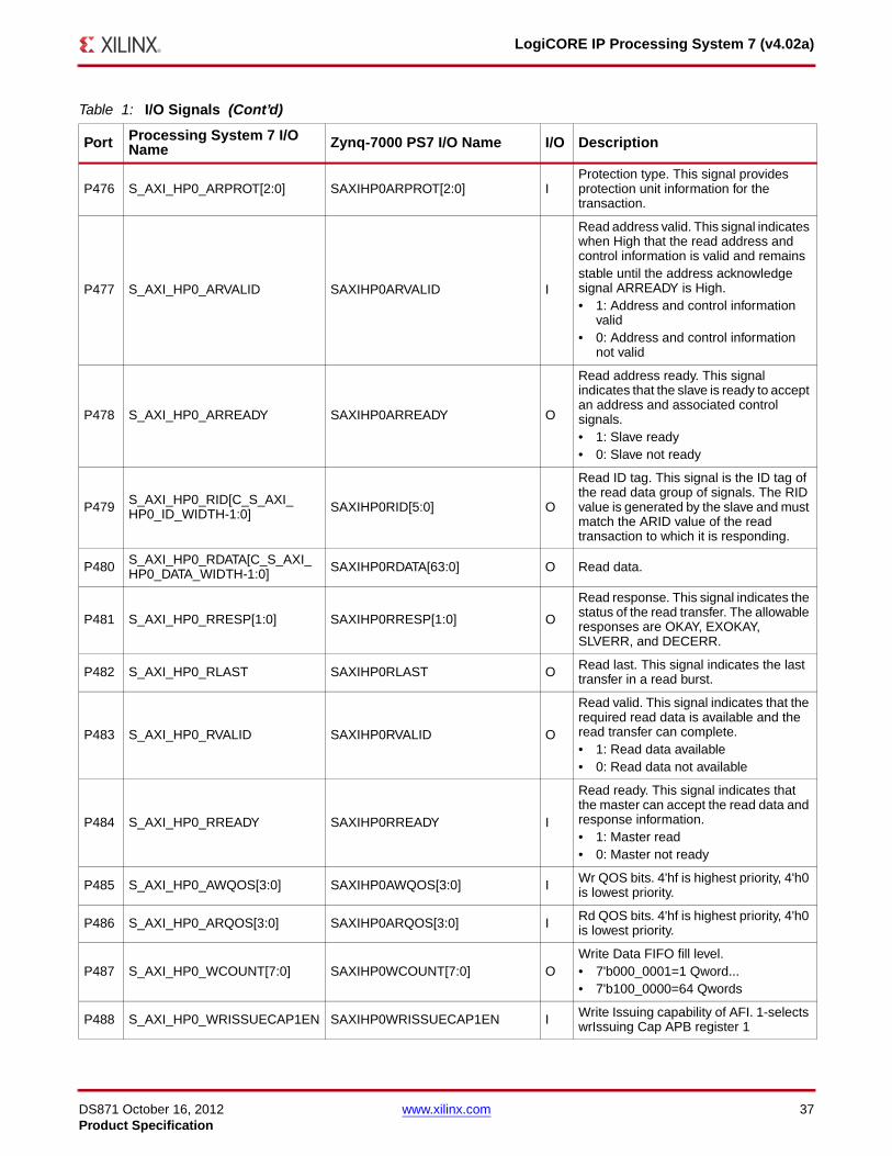
DS871 October 16, 2012 www.xilinx.com 37Product Specification
LogiCORE IP Processing System 7 (v4.02a)
P476 S_AXI_HP0_ARPROT[2:0] SAXIHP0ARPROT[2:0] IProtection type. This signal provides protection unit information for the transaction.
P477 S_AXI_HP0_ARVALID SAXIHP0ARVALID I
Read address valid. This signal indicates when High that the read address and control information is valid and remainsstable until the address acknowledge signal ARREADY is High.• 1: Address and control information
valid• 0: Address and control information
not valid
P478 S_AXI_HP0_ARREADY SAXIHP0ARREADY O
Read address ready. This signal indicates that the slave is ready to accept an address and associated control signals.• 1: Slave ready• 0: Slave not ready
P479 S_AXI_HP0_RID[C_S_AXI_HP0_ID_WIDTH-1:0] SAXIHP0RID[5:0] O
Read ID tag. This signal is the ID tag of the read data group of signals. The RID value is generated by the slave and must match the ARID value of the read transaction to which it is responding.
P480 S_AXI_HP0_RDATA[C_S_AXI_HP0_DATA_WIDTH-1:0] SAXIHP0RDATA[63:0] O Read data.
P481 S_AXI_HP0_RRESP[1:0] SAXIHP0RRESP[1:0] O
Read response. This signal indicates the status of the read transfer. The allowable responses are OKAY, EXOKAY, SLVERR, and DECERR.
P482 S_AXI_HP0_RLAST SAXIHP0RLAST O Read last. This signal indicates the last transfer in a read burst.
P483 S_AXI_HP0_RVALID SAXIHP0RVALID O
Read valid. This signal indicates that the required read data is available and the read transfer can complete.• 1: Read data available• 0: Read data not available
P484 S_AXI_HP0_RREADY SAXIHP0RREADY I
Read ready. This signal indicates that the master can accept the read data and response information.• 1: Master read• 0: Master not ready
P485 S_AXI_HP0_AWQOS[3:0] SAXIHP0AWQOS[3:0] I Wr QOS bits. 4'hf is highest priority, 4'h0 is lowest priority.
P486 S_AXI_HP0_ARQOS[3:0] SAXIHP0ARQOS[3:0] I Rd QOS bits. 4'hf is highest priority, 4'h0 is lowest priority.
P487 S_AXI_HP0_WCOUNT[7:0] SAXIHP0WCOUNT[7:0] OWrite Data FIFO fill level.• 7'b000_0001=1 Qword...• 7'b100_0000=64 Qwords
P488 S_AXI_HP0_WRISSUECAP1EN SAXIHP0WRISSUECAP1EN I Write Issuing capability of AFI. 1-selects wrIssuing Cap APB register 1
Table 1: I/O Signals (Cont’d)
Port Processing System 7 I/O Name Zynq-7000 PS7 I/O Name I/O Description
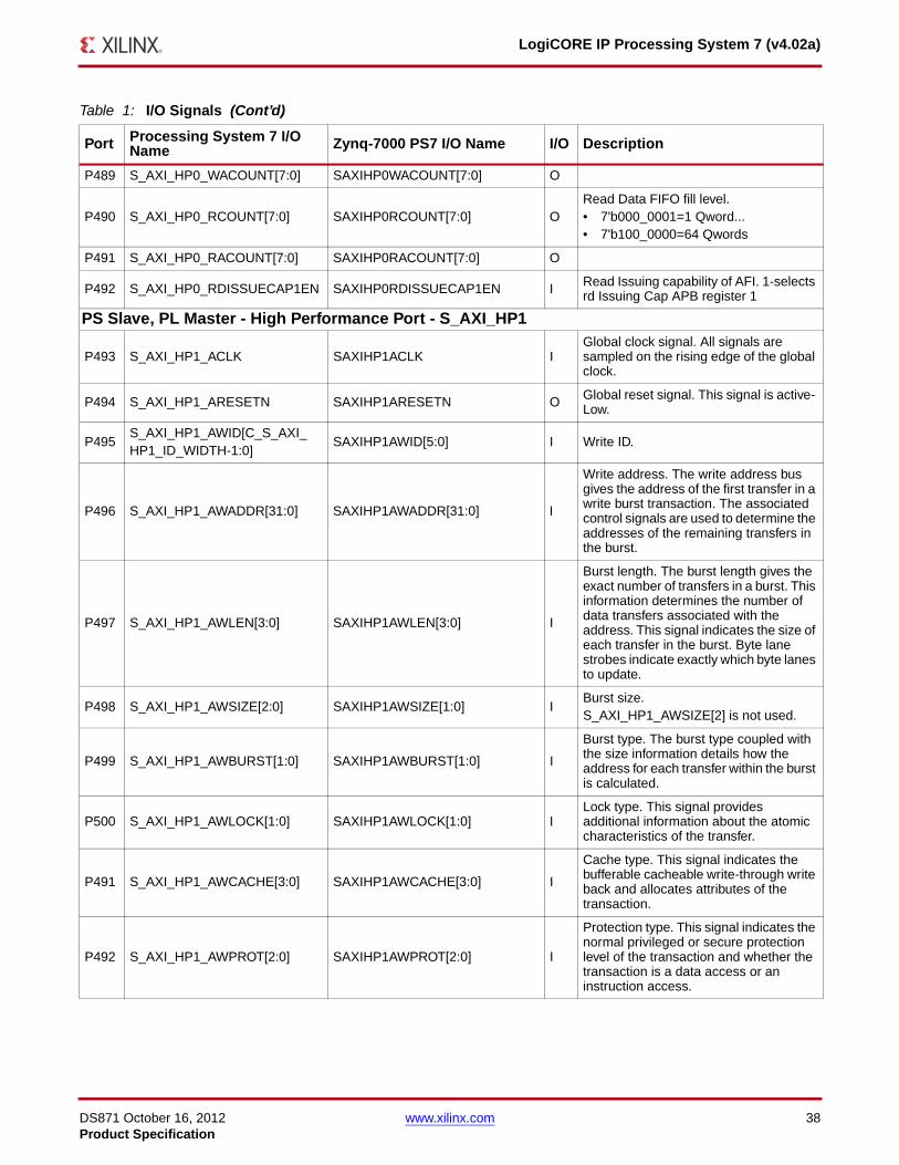
DS871 October 16, 2012 www.xilinx.com 38Product Specification
LogiCORE IP Processing System 7 (v4.02a)
P489 S_AXI_HP0_WACOUNT[7:0] SAXIHP0WACOUNT[7:0] O
P490 S_AXI_HP0_RCOUNT[7:0] SAXIHP0RCOUNT[7:0] ORead Data FIFO fill level.• 7'b000_0001=1 Qword...• 7'b100_0000=64 Qwords
P491 S_AXI_HP0_RACOUNT[7:0] SAXIHP0RACOUNT[7:0] O
P492 S_AXI_HP0_RDISSUECAP1EN SAXIHP0RDISSUECAP1EN I Read Issuing capability of AFI. 1-selects rd Issuing Cap APB register 1
PS Slave, PL Master - High Performance Port - S_AXI_HP1
P493 S_AXI_HP1_ACLK SAXIHP1ACLK IGlobal clock signal. All signals are sampled on the rising edge of the global clock.
P494 S_AXI_HP1_ARESETN SAXIHP1ARESETN O Global reset signal. This signal is active- Low.
P495S_AXI_HP1_AWID[C_S_AXI_HP1_ID_WIDTH-1:0]
SAXIHP1AWID[5:0] I Write ID.
P496 S_AXI_HP1_AWADDR[31:0] SAXIHP1AWADDR[31:0] I
Write address. The write address bus gives the address of the first transfer in a write burst transaction. The associated control signals are used to determine the addresses of the remaining transfers in the burst.
P497 S_AXI_HP1_AWLEN[3:0] SAXIHP1AWLEN[3:0] I
Burst length. The burst length gives the exact number of transfers in a burst. This information determines the number of data transfers associated with the address. This signal indicates the size of each transfer in the burst. Byte lane strobes indicate exactly which byte lanes to update.
P498 S_AXI_HP1_AWSIZE[2:0] SAXIHP1AWSIZE[1:0] IBurst size.S_AXI_HP1_AWSIZE[2] is not used.
P499 S_AXI_HP1_AWBURST[1:0] SAXIHP1AWBURST[1:0] I
Burst type. The burst type coupled with the size information details how the address for each transfer within the burst is calculated.
P500 S_AXI_HP1_AWLOCK[1:0] SAXIHP1AWLOCK[1:0] ILock type. This signal provides additional information about the atomic characteristics of the transfer.
P491 S_AXI_HP1_AWCACHE[3:0] SAXIHP1AWCACHE[3:0] I
Cache type. This signal indicates the bufferable cacheable write-through write back and allocates attributes of the transaction.
P492 S_AXI_HP1_AWPROT[2:0] SAXIHP1AWPROT[2:0] I
Protection type. This signal indicates the normal privileged or secure protection level of the transaction and whether the transaction is a data access or an instruction access.
Table 1: I/O Signals (Cont’d)
Port Processing System 7 I/O Name Zynq-7000 PS7 I/O Name I/O Description
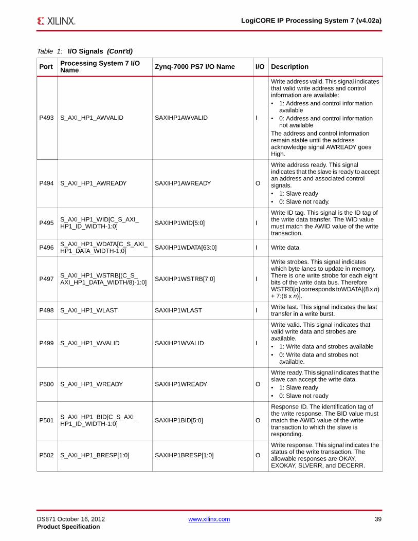
DS871 October 16, 2012 www.xilinx.com 39Product Specification
LogiCORE IP Processing System 7 (v4.02a)
P493 S_AXI_HP1_AWVALID SAXIHP1AWVALID I
Write address valid. This signal indicates that valid write address and control information are available:• 1: Address and control information
available• 0: Address and control information
not availableThe address and control information remain stable until the address acknowledge signal AWREADY goes High.
P494 S_AXI_HP1_AWREADY SAXIHP1AWREADY O
Write address ready. This signal indicates that the slave is ready to accept an address and associated control signals.• 1: Slave ready• 0: Slave not ready.
P495 S_AXI_HP1_WID[C_S_AXI_HP1_ID_WIDTH-1:0] SAXIHP1WID[5:0] I
Write ID tag. This signal is the ID tag of the write data transfer. The WID value must match the AWID value of the write transaction.
P496 S_AXI_HP1_WDATA[C_S_AXI_HP1_DATA_WIDTH-1:0] SAXIHP1WDATA[63:0] I Write data.
P497 S_AXI_HP1_WSTRB[(C_S_AXI_HP1_DATA_WIDTH/8)-1:0] SAXIHP1WSTRB[7:0] I
Write strobes. This signal indicates which byte lanes to update in memory. There is one write strobe for each eight bits of the write data bus. Therefore WSTRB[n] corresponds toWDATA[(8 x n) + 7:(8 x n)].
P498 S_AXI_HP1_WLAST SAXIHP1WLAST I Write last. This signal indicates the last transfer in a write burst.
P499 S_AXI_HP1_WVALID SAXIHP1WVALID I
Write valid. This signal indicates that valid write data and strobes are available.• 1: Write data and strobes available• 0: Write data and strobes not
available.
P500 S_AXI_HP1_WREADY SAXIHP1WREADY O
Write ready. This signal indicates that the slave can accept the write data.• 1: Slave ready• 0: Slave not ready
P501 S_AXI_HP1_BID[C_S_AXI_HP1_ID_WIDTH-1:0] SAXIHP1BID[5:0] O
Response ID. The identification tag of the write response. The BID value must match the AWID value of the write transaction to which the slave is responding.
P502 S_AXI_HP1_BRESP[1:0] SAXIHP1BRESP[1:0] O
Write response. This signal indicates the status of the write transaction. The allowable responses are OKAY, EXOKAY, SLVERR, and DECERR.
Table 1: I/O Signals (Cont’d)
Port Processing System 7 I/O Name Zynq-7000 PS7 I/O Name I/O Description
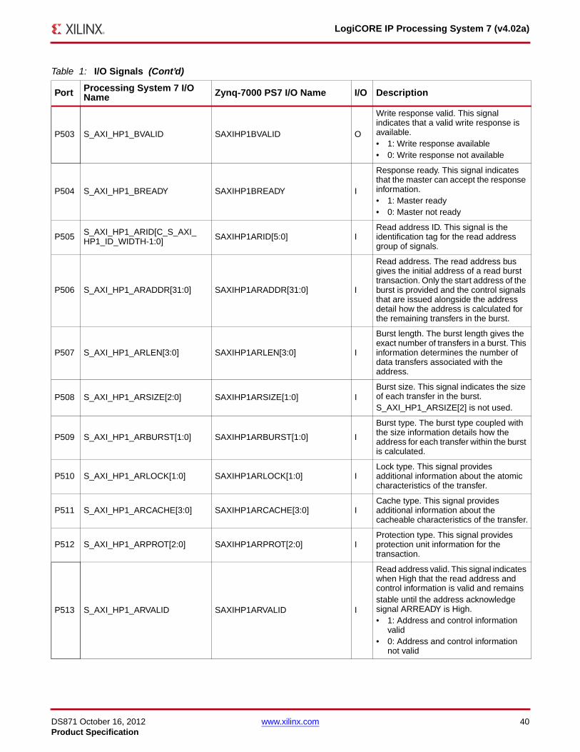
DS871 October 16, 2012 www.xilinx.com 40Product Specification
LogiCORE IP Processing System 7 (v4.02a)
P503 S_AXI_HP1_BVALID SAXIHP1BVALID O
Write response valid. This signal indicates that a valid write response is available.• 1: Write response available• 0: Write response not available
P504 S_AXI_HP1_BREADY SAXIHP1BREADY I
Response ready. This signal indicates that the master can accept the response information.• 1: Master ready• 0: Master not ready
P505 S_AXI_HP1_ARID[C_S_AXI_HP1_ID_WIDTH-1:0] SAXIHP1ARID[5:0] I
Read address ID. This signal is the identification tag for the read address group of signals.
P506 S_AXI_HP1_ARADDR[31:0] SAXIHP1ARADDR[31:0] I
Read address. The read address bus gives the initial address of a read burst transaction. Only the start address of the burst is provided and the control signals that are issued alongside the address detail how the address is calculated for the remaining transfers in the burst.
P507 S_AXI_HP1_ARLEN[3:0] SAXIHP1ARLEN[3:0] I
Burst length. The burst length gives the exact number of transfers in a burst. This information determines the number of data transfers associated with the address.
P508 S_AXI_HP1_ARSIZE[2:0] SAXIHP1ARSIZE[1:0] IBurst size. This signal indicates the size of each transfer in the burst. S_AXI_HP1_ARSIZE[2] is not used.
P509 S_AXI_HP1_ARBURST[1:0] SAXIHP1ARBURST[1:0] I
Burst type. The burst type coupled with the size information details how the address for each transfer within the burst is calculated.
P510 S_AXI_HP1_ARLOCK[1:0] SAXIHP1ARLOCK[1:0] ILock type. This signal provides additional information about the atomic characteristics of the transfer.
P511 S_AXI_HP1_ARCACHE[3:0] SAXIHP1ARCACHE[3:0] ICache type. This signal provides additional information about the cacheable characteristics of the transfer.
P512 S_AXI_HP1_ARPROT[2:0] SAXIHP1ARPROT[2:0] IProtection type. This signal provides protection unit information for the transaction.
P513 S_AXI_HP1_ARVALID SAXIHP1ARVALID I
Read address valid. This signal indicates when High that the read address and control information is valid and remainsstable until the address acknowledge signal ARREADY is High.• 1: Address and control information
valid• 0: Address and control information
not valid
Table 1: I/O Signals (Cont’d)
Port Processing System 7 I/O Name Zynq-7000 PS7 I/O Name I/O Description
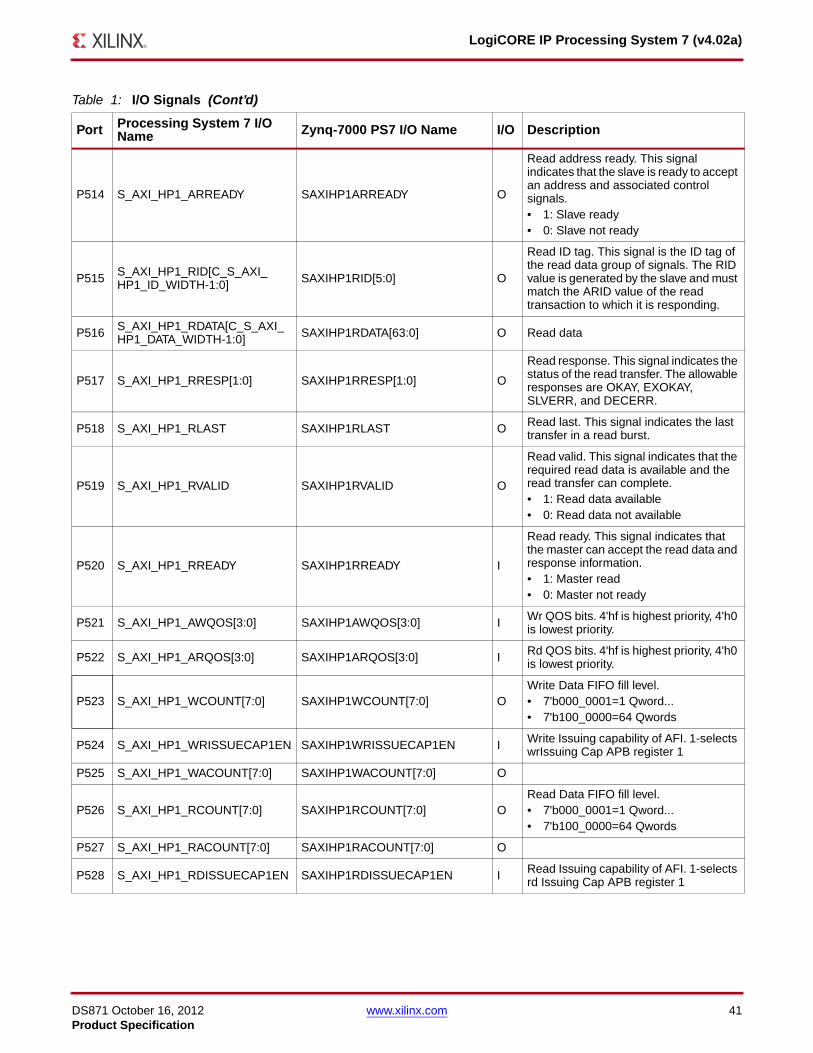
DS871 October 16, 2012 www.xilinx.com 41Product Specification
LogiCORE IP Processing System 7 (v4.02a)
P514 S_AXI_HP1_ARREADY SAXIHP1ARREADY O
Read address ready. This signal indicates that the slave is ready to accept an address and associated control signals.• 1: Slave ready• 0: Slave not ready
P515 S_AXI_HP1_RID[C_S_AXI_HP1_ID_WIDTH-1:0] SAXIHP1RID[5:0] O
Read ID tag. This signal is the ID tag of the read data group of signals. The RID value is generated by the slave and must match the ARID value of the read transaction to which it is responding.
P516 S_AXI_HP1_RDATA[C_S_AXI_HP1_DATA_WIDTH-1:0] SAXIHP1RDATA[63:0] O Read data
P517 S_AXI_HP1_RRESP[1:0] SAXIHP1RRESP[1:0] O
Read response. This signal indicates the status of the read transfer. The allowable responses are OKAY, EXOKAY, SLVERR, and DECERR.
P518 S_AXI_HP1_RLAST SAXIHP1RLAST O Read last. This signal indicates the last transfer in a read burst.
P519 S_AXI_HP1_RVALID SAXIHP1RVALID O
Read valid. This signal indicates that the required read data is available and the read transfer can complete.• 1: Read data available• 0: Read data not available
P520 S_AXI_HP1_RREADY SAXIHP1RREADY I
Read ready. This signal indicates that the master can accept the read data and response information.• 1: Master read• 0: Master not ready
P521 S_AXI_HP1_AWQOS[3:0] SAXIHP1AWQOS[3:0] I Wr QOS bits. 4'hf is highest priority, 4'h0 is lowest priority.
P522 S_AXI_HP1_ARQOS[3:0] SAXIHP1ARQOS[3:0] I Rd QOS bits. 4'hf is highest priority, 4'h0 is lowest priority.
P523 S_AXI_HP1_WCOUNT[7:0] SAXIHP1WCOUNT[7:0] OWrite Data FIFO fill level.• 7'b000_0001=1 Qword...• 7'b100_0000=64 Qwords
P524 S_AXI_HP1_WRISSUECAP1EN SAXIHP1WRISSUECAP1EN I Write Issuing capability of AFI. 1-selects wrIssuing Cap APB register 1
P525 S_AXI_HP1_WACOUNT[7:0] SAXIHP1WACOUNT[7:0] O
P526 S_AXI_HP1_RCOUNT[7:0] SAXIHP1RCOUNT[7:0] ORead Data FIFO fill level.• 7'b000_0001=1 Qword...• 7'b100_0000=64 Qwords
P527 S_AXI_HP1_RACOUNT[7:0] SAXIHP1RACOUNT[7:0] O
P528 S_AXI_HP1_RDISSUECAP1EN SAXIHP1RDISSUECAP1EN I Read Issuing capability of AFI. 1-selects rd Issuing Cap APB register 1
Table 1: I/O Signals (Cont’d)
Port Processing System 7 I/O Name Zynq-7000 PS7 I/O Name I/O Description
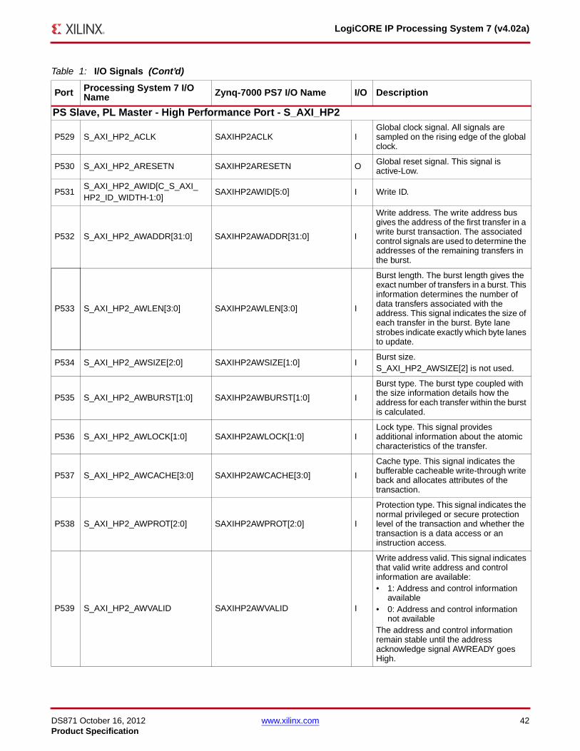
DS871 October 16, 2012 www.xilinx.com 42Product Specification
LogiCORE IP Processing System 7 (v4.02a)
PS Slave, PL Master - High Performance Port - S_AXI_HP2
P529 S_AXI_HP2_ACLK SAXIHP2ACLK IGlobal clock signal. All signals are sampled on the rising edge of the global clock.
P530 S_AXI_HP2_ARESETN SAXIHP2ARESETN O Global reset signal. This signal is active-Low.
P531S_AXI_HP2_AWID[C_S_AXI_HP2_ID_WIDTH-1:0]
SAXIHP2AWID[5:0] I Write ID.
P532 S_AXI_HP2_AWADDR[31:0] SAXIHP2AWADDR[31:0] I
Write address. The write address bus gives the address of the first transfer in a write burst transaction. The associated control signals are used to determine the addresses of the remaining transfers in the burst.
P533 S_AXI_HP2_AWLEN[3:0] SAXIHP2AWLEN[3:0] I
Burst length. The burst length gives the exact number of transfers in a burst. This information determines the number of data transfers associated with the address. This signal indicates the size of each transfer in the burst. Byte lane strobes indicate exactly which byte lanes to update.
P534 S_AXI_HP2_AWSIZE[2:0] SAXIHP2AWSIZE[1:0] IBurst size.S_AXI_HP2_AWSIZE[2] is not used.
P535 S_AXI_HP2_AWBURST[1:0] SAXIHP2AWBURST[1:0] I
Burst type. The burst type coupled with the size information details how the address for each transfer within the burst is calculated.
P536 S_AXI_HP2_AWLOCK[1:0] SAXIHP2AWLOCK[1:0] ILock type. This signal provides additional information about the atomic characteristics of the transfer.
P537 S_AXI_HP2_AWCACHE[3:0] SAXIHP2AWCACHE[3:0] I
Cache type. This signal indicates the bufferable cacheable write-through write back and allocates attributes of the transaction.
P538 S_AXI_HP2_AWPROT[2:0] SAXIHP2AWPROT[2:0] I
Protection type. This signal indicates the normal privileged or secure protection level of the transaction and whether the transaction is a data access or an instruction access.
P539 S_AXI_HP2_AWVALID SAXIHP2AWVALID I
Write address valid. This signal indicates that valid write address and control information are available:• 1: Address and control information
available• 0: Address and control information
not availableThe address and control information remain stable until the address acknowledge signal AWREADY goes High.
Table 1: I/O Signals (Cont’d)
Port Processing System 7 I/O Name Zynq-7000 PS7 I/O Name I/O Description
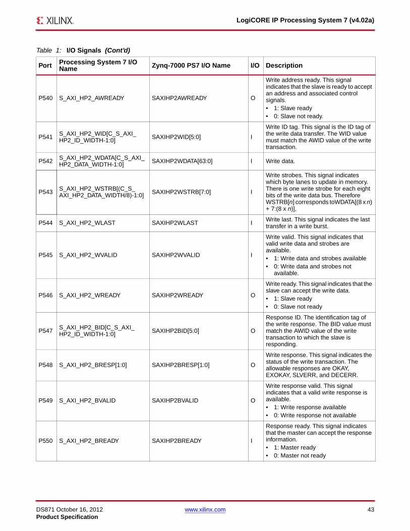
DS871 October 16, 2012 www.xilinx.com 43Product Specification
LogiCORE IP Processing System 7 (v4.02a)
P540 S_AXI_HP2_AWREADY SAXIHP2AWREADY O
Write address ready. This signal indicates that the slave is ready to accept an address and associated control signals.• 1: Slave ready• 0: Slave not ready.
P541 S_AXI_HP2_WID[C_S_AXI_HP2_ID_WIDTH-1:0] SAXIHP2WID[5:0] I
Write ID tag. This signal is the ID tag of the write data transfer. The WID value must match the AWID value of the write transaction.
P542 S_AXI_HP2_WDATA[C_S_AXI_HP2_DATA_WIDTH-1:0] SAXIHP2WDATA[63:0] I Write data.
P543 S_AXI_HP2_WSTRB[(C_S_AXI_HP2_DATA_WIDTH/8)-1:0] SAXIHP2WSTRB[7:0] I
Write strobes. This signal indicates which byte lanes to update in memory. There is one write strobe for each eight bits of the write data bus. Therefore WSTRB[n] corresponds toWDATA[(8 x n) + 7:(8 x n)],
P544 S_AXI_HP2_WLAST SAXIHP2WLAST I Write last. This signal indicates the last transfer in a write burst.
P545 S_AXI_HP2_WVALID SAXIHP2WVALID I
Write valid. This signal indicates that valid write data and strobes are available.• 1: Write data and strobes available• 0: Write data and strobes not
available.
P546 S_AXI_HP2_WREADY SAXIHP2WREADY O
Write ready. This signal indicates that the slave can accept the write data.• 1: Slave ready• 0: Slave not ready
P547 S_AXI_HP2_BID[C_S_AXI_HP2_ID_WIDTH-1:0] SAXIHP2BID[5:0] O
Response ID. The identification tag of the write response. The BID value must match the AWID value of the write transaction to which the slave is responding.
P548 S_AXI_HP2_BRESP[1:0] SAXIHP2BRESP[1:0] O
Write response. This signal indicates the status of the write transaction. The allowable responses are OKAY, EXOKAY, SLVERR, and DECERR.
P549 S_AXI_HP2_BVALID SAXIHP2BVALID O
Write response valid. This signal indicates that a valid write response is available.• 1: Write response available• 0: Write response not available
P550 S_AXI_HP2_BREADY SAXIHP2BREADY I
Response ready. This signal indicates that the master can accept the response information.• 1: Master ready• 0: Master not ready
Table 1: I/O Signals (Cont’d)
Port Processing System 7 I/O Name Zynq-7000 PS7 I/O Name I/O Description
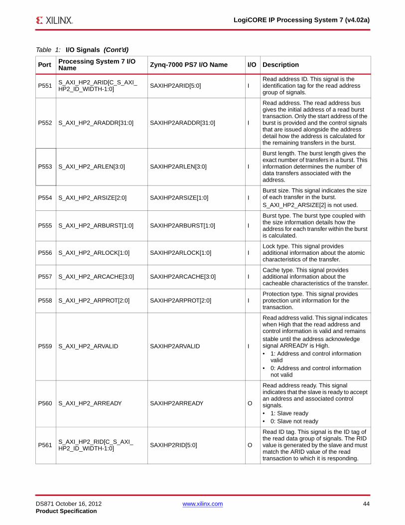
DS871 October 16, 2012 www.xilinx.com 44Product Specification
LogiCORE IP Processing System 7 (v4.02a)
P551 S_AXI_HP2_ARID[C_S_AXI_HP2_ID_WIDTH-1:0] SAXIHP2ARID[5:0] I
Read address ID. This signal is the identification tag for the read address group of signals.
P552 S_AXI_HP2_ARADDR[31:0] SAXIHP2ARADDR[31:0] I
Read address. The read address bus gives the initial address of a read burst transaction. Only the start address of the burst is provided and the control signals that are issued alongside the address detail how the address is calculated for the remaining transfers in the burst.
P553 S_AXI_HP2_ARLEN[3:0] SAXIHP2ARLEN[3:0] I
Burst length. The burst length gives the exact number of transfers in a burst. This information determines the number of data transfers associated with the address.
P554 S_AXI_HP2_ARSIZE[2:0] SAXIHP2ARSIZE[1:0] IBurst size. This signal indicates the size of each transfer in the burst. S_AXI_HP2_ARSIZE[2] is not used.
P555 S_AXI_HP2_ARBURST[1:0] SAXIHP2ARBURST[1:0] I
Burst type. The burst type coupled with the size information details how the address for each transfer within the burst is calculated.
P556 S_AXI_HP2_ARLOCK[1:0] SAXIHP2ARLOCK[1:0] ILock type. This signal provides additional information about the atomic characteristics of the transfer.
P557 S_AXI_HP2_ARCACHE[3:0] SAXIHP2ARCACHE[3:0] ICache type. This signal provides additional information about the cacheable characteristics of the transfer.
P558 S_AXI_HP2_ARPROT[2:0] SAXIHP2ARPROT[2:0] IProtection type. This signal provides protection unit information for the transaction.
P559 S_AXI_HP2_ARVALID SAXIHP2ARVALID I
Read address valid. This signal indicates when High that the read address and control information is valid and remainsstable until the address acknowledge signal ARREADY is High.• 1: Address and control information
valid• 0: Address and control information
not valid
P560 S_AXI_HP2_ARREADY SAXIHP2ARREADY O
Read address ready. This signal indicates that the slave is ready to accept an address and associated control signals.• 1: Slave ready• 0: Slave not ready
P561 S_AXI_HP2_RID[C_S_AXI_HP2_ID_WIDTH-1:0] SAXIHP2RID[5:0] O
Read ID tag. This signal is the ID tag of the read data group of signals. The RID value is generated by the slave and must match the ARID value of the read transaction to which it is responding.
Table 1: I/O Signals (Cont’d)
Port Processing System 7 I/O Name Zynq-7000 PS7 I/O Name I/O Description
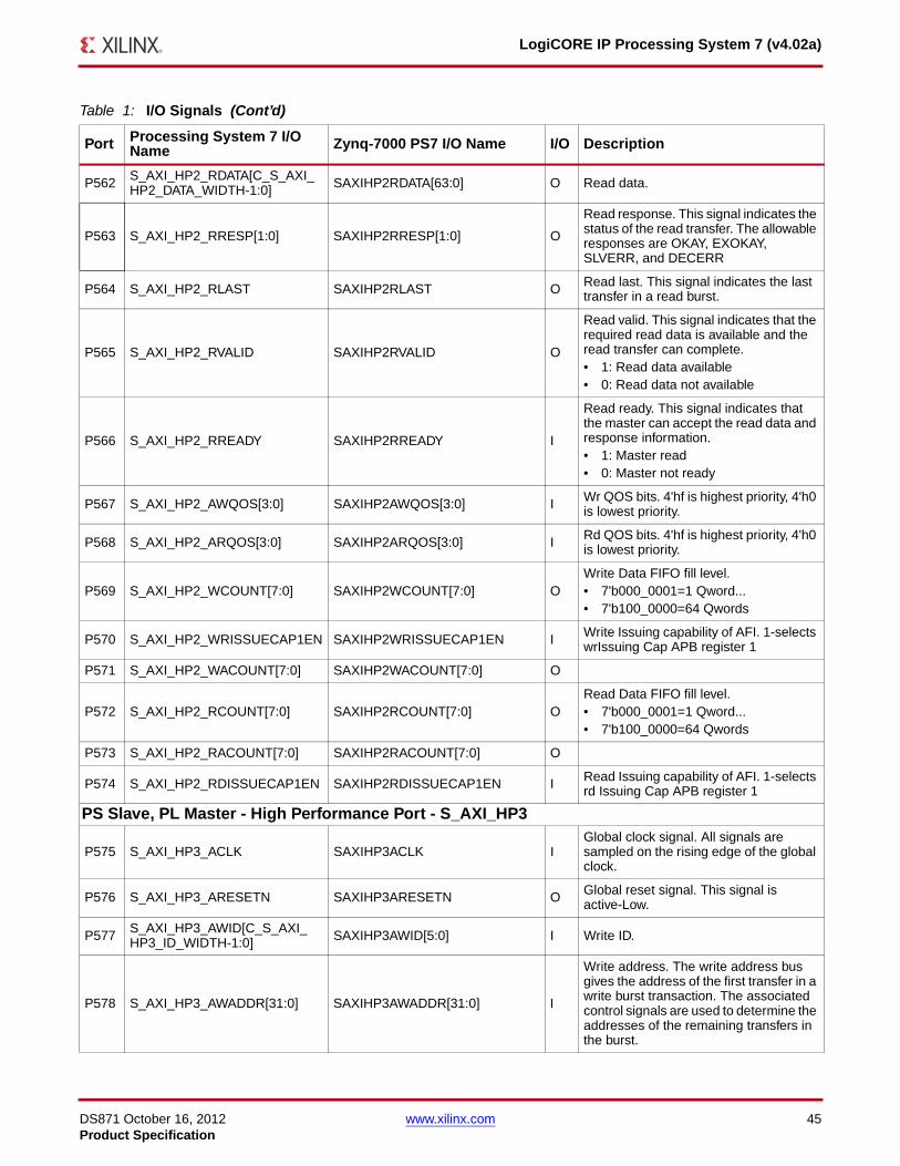
DS871 October 16, 2012 www.xilinx.com 45Product Specification
LogiCORE IP Processing System 7 (v4.02a)
P562 S_AXI_HP2_RDATA[C_S_AXI_HP2_DATA_WIDTH-1:0] SAXIHP2RDATA[63:0] O Read data.
P563 S_AXI_HP2_RRESP[1:0] SAXIHP2RRESP[1:0] O
Read response. This signal indicates the status of the read transfer. The allowable responses are OKAY, EXOKAY, SLVERR, and DECERR
P564 S_AXI_HP2_RLAST SAXIHP2RLAST O Read last. This signal indicates the last transfer in a read burst.
P565 S_AXI_HP2_RVALID SAXIHP2RVALID O
Read valid. This signal indicates that the required read data is available and the read transfer can complete.• 1: Read data available• 0: Read data not available
P566 S_AXI_HP2_RREADY SAXIHP2RREADY I
Read ready. This signal indicates that the master can accept the read data and response information.• 1: Master read• 0: Master not ready
P567 S_AXI_HP2_AWQOS[3:0] SAXIHP2AWQOS[3:0] I Wr QOS bits. 4'hf is highest priority, 4'h0 is lowest priority.
P568 S_AXI_HP2_ARQOS[3:0] SAXIHP2ARQOS[3:0] I Rd QOS bits. 4'hf is highest priority, 4'h0 is lowest priority.
P569 S_AXI_HP2_WCOUNT[7:0] SAXIHP2WCOUNT[7:0] OWrite Data FIFO fill level.• 7'b000_0001=1 Qword...• 7'b100_0000=64 Qwords
P570 S_AXI_HP2_WRISSUECAP1EN SAXIHP2WRISSUECAP1EN I Write Issuing capability of AFI. 1-selects wrIssuing Cap APB register 1
P571 S_AXI_HP2_WACOUNT[7:0] SAXIHP2WACOUNT[7:0] O
P572 S_AXI_HP2_RCOUNT[7:0] SAXIHP2RCOUNT[7:0] ORead Data FIFO fill level.• 7'b000_0001=1 Qword...• 7'b100_0000=64 Qwords
P573 S_AXI_HP2_RACOUNT[7:0] SAXIHP2RACOUNT[7:0] O
P574 S_AXI_HP2_RDISSUECAP1EN SAXIHP2RDISSUECAP1EN I Read Issuing capability of AFI. 1-selects rd Issuing Cap APB register 1
PS Slave, PL Master - High Performance Port - S_AXI_HP3
P575 S_AXI_HP3_ACLK SAXIHP3ACLK IGlobal clock signal. All signals are sampled on the rising edge of the global clock.
P576 S_AXI_HP3_ARESETN SAXIHP3ARESETN O Global reset signal. This signal is active-Low.
P577 S_AXI_HP3_AWID[C_S_AXI_HP3_ID_WIDTH-1:0] SAXIHP3AWID[5:0] I Write ID.
P578 S_AXI_HP3_AWADDR[31:0] SAXIHP3AWADDR[31:0] I
Write address. The write address bus gives the address of the first transfer in a write burst transaction. The associated control signals are used to determine the addresses of the remaining transfers in the burst.
Table 1: I/O Signals (Cont’d)
Port Processing System 7 I/O Name Zynq-7000 PS7 I/O Name I/O Description
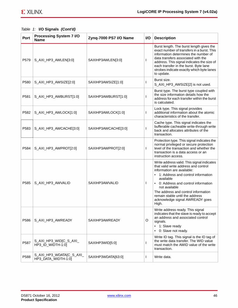
DS871 October 16, 2012 www.xilinx.com 46Product Specification
LogiCORE IP Processing System 7 (v4.02a)
P579 S_AXI_HP3_AWLEN[3:0] SAXIHP3AWLEN[3:0] I
Burst length. The burst length gives the exact number of transfers in a burst. This information determines the number of data transfers associated with the address. This signal indicates the size of each transfer in the burst. Byte lane strobes indicate exactly which byte lanes to update.
P580 S_AXI_HP3_AWSIZE[2:0] SAXIHP3AWSIZE[1:0] IBurst size.S_AXI_HP3_AWSIZE[2] is not used.
P581 S_AXI_HP3_AWBURST[1:0] SAXIHP3AWBURST[1:0] I
Burst type. The burst type coupled with the size information details how the address for each transfer within the burst is calculated.
P582 S_AXI_HP3_AWLOCK[1:0] SAXIHP3AWLOCK[1:0] ILock type. This signal provides additional information about the atomic characteristics of the transfer.
P583 S_AXI_HP3_AWCACHE[3:0] SAXIHP3AWCACHE[3:0] I
Cache type. This signal indicates the bufferable cacheable write-through write back and allocates attributes of the transaction.
P584 S_AXI_HP3_AWPROT[2:0] SAXIHP3AWPROT[2:0] I
Protection type. This signal indicates the normal privileged or secure protection level of the transaction and whether the transaction is a data access or an instruction access.
P585 S_AXI_HP3_AWVALID SAXIHP3AWVALID I
Write address valid. This signal indicates that valid write address and control information are available:• 1: Address and control information
available• 0: Address and control information
not availableThe address and control information remain stable until the address acknowledge signal AWREADY goes High.
P586 S_AXI_HP3_AWREADY SAXIHP3AWREADY O
Write address ready. This signal indicates that the slave is ready to accept an address and associated control signals.• 1: Slave ready• 0: Slave not ready.
P587 S_AXI_HP3_WID[C_S_AXI_HP3_ID_WIDTH-1:0] SAXIHP3WID[5:0] I
Write ID tag. This signal is the ID tag of the write data transfer. The WID value must match the AWID value of the write transaction.
P588 S_AXI_HP3_WDATA[C_S_AXI_HP3_DATA_WIDTH-1:0] SAXIHP3WDATA[63:0] I Write data.
Table 1: I/O Signals (Cont’d)
Port Processing System 7 I/O Name Zynq-7000 PS7 I/O Name I/O Description
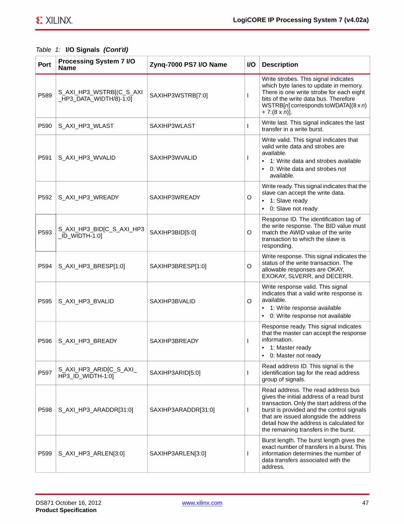
DS871 October 16, 2012 www.xilinx.com 47Product Specification
LogiCORE IP Processing System 7 (v4.02a)
P589 S_AXI_HP3_WSTRB[(C_S_AXI_HP3_DATA_WIDTH/8)-1:0] SAXIHP3WSTRB[7:0] I
Write strobes. This signal indicates which byte lanes to update in memory. There is one write strobe for each eight bits of the write data bus. Therefore WSTRB[n] corresponds toWDATA[(8 x n) + 7:(8 x n)].
P590 S_AXI_HP3_WLAST SAXIHP3WLAST I Write last. This signal indicates the last transfer in a write burst.
P591 S_AXI_HP3_WVALID SAXIHP3WVALID I
Write valid. This signal indicates that valid write data and strobes are available.• 1: Write data and strobes available• 0: Write data and strobes not
available.
P592 S_AXI_HP3_WREADY SAXIHP3WREADY O
Write ready. This signal indicates that the slave can accept the write data.• 1: Slave ready• 0: Slave not ready
P593 S_AXI_HP3_BID[C_S_AXI_HP3_ID_WIDTH-1:0] SAXIHP3BID[5:0] O
Response ID. The identification tag of the write response. The BID value must match the AWID value of the write transaction to which the slave is responding.
P594 S_AXI_HP3_BRESP[1:0] SAXIHP3BRESP[1:0] O
Write response. This signal indicates the status of the write transaction. The allowable responses are OKAY, EXOKAY, SLVERR, and DECERR.
P595 S_AXI_HP3_BVALID SAXIHP3BVALID O
Write response valid. This signal indicates that a valid write response is available.• 1: Write response available• 0: Write response not available
P596 S_AXI_HP3_BREADY SAXIHP3BREADY I
Response ready. This signal indicates that the master can accept the response information.• 1: Master ready• 0: Master not ready
P597 S_AXI_HP3_ARID[C_S_AXI_HP3_ID_WIDTH-1:0] SAXIHP3ARID[5:0] I
Read address ID. This signal is the identification tag for the read address group of signals.
P598 S_AXI_HP3_ARADDR[31:0] SAXIHP3ARADDR[31:0] I
Read address. The read address bus gives the initial address of a read burst transaction. Only the start address of the burst is provided and the control signals that are issued alongside the address detail how the address is calculated for the remaining transfers in the burst.
P599 S_AXI_HP3_ARLEN[3:0] SAXIHP3ARLEN[3:0] I
Burst length. The burst length gives the exact number of transfers in a burst. This information determines the number of data transfers associated with the address.
Table 1: I/O Signals (Cont’d)
Port Processing System 7 I/O Name Zynq-7000 PS7 I/O Name I/O Description
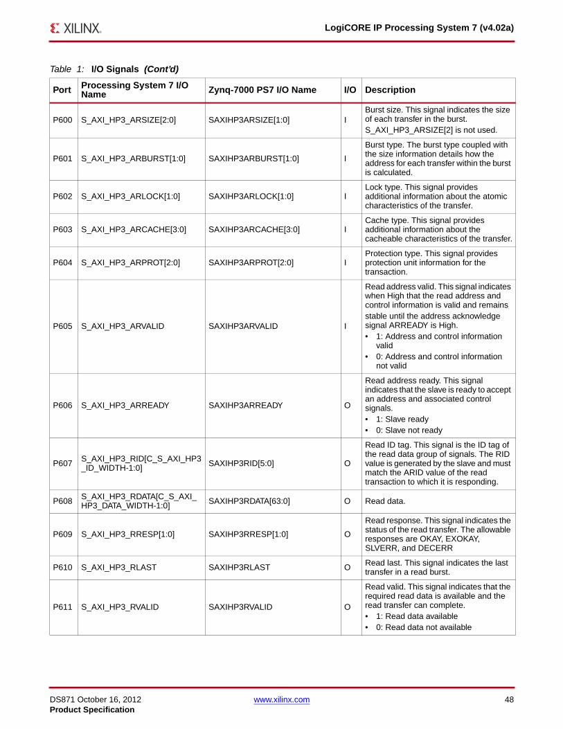
DS871 October 16, 2012 www.xilinx.com 48Product Specification
LogiCORE IP Processing System 7 (v4.02a)
P600 S_AXI_HP3_ARSIZE[2:0] SAXIHP3ARSIZE[1:0] IBurst size. This signal indicates the size of each transfer in the burst. S_AXI_HP3_ARSIZE[2] is not used.
P601 S_AXI_HP3_ARBURST[1:0] SAXIHP3ARBURST[1:0] I
Burst type. The burst type coupled with the size information details how the address for each transfer within the burst is calculated.
P602 S_AXI_HP3_ARLOCK[1:0] SAXIHP3ARLOCK[1:0] ILock type. This signal provides additional information about the atomic characteristics of the transfer.
P603 S_AXI_HP3_ARCACHE[3:0] SAXIHP3ARCACHE[3:0] ICache type. This signal provides additional information about the cacheable characteristics of the transfer.
P604 S_AXI_HP3_ARPROT[2:0] SAXIHP3ARPROT[2:0] IProtection type. This signal provides protection unit information for the transaction.
P605 S_AXI_HP3_ARVALID SAXIHP3ARVALID I
Read address valid. This signal indicates when High that the read address and control information is valid and remainsstable until the address acknowledge signal ARREADY is High.• 1: Address and control information
valid• 0: Address and control information
not valid
P606 S_AXI_HP3_ARREADY SAXIHP3ARREADY O
Read address ready. This signal indicates that the slave is ready to accept an address and associated control signals.• 1: Slave ready• 0: Slave not ready
P607 S_AXI_HP3_RID[C_S_AXI_HP3_ID_WIDTH-1:0] SAXIHP3RID[5:0] O
Read ID tag. This signal is the ID tag of the read data group of signals. The RID value is generated by the slave and must match the ARID value of the read transaction to which it is responding.
P608 S_AXI_HP3_RDATA[C_S_AXI_HP3_DATA_WIDTH-1:0] SAXIHP3RDATA[63:0] O Read data.
P609 S_AXI_HP3_RRESP[1:0] SAXIHP3RRESP[1:0] O
Read response. This signal indicates the status of the read transfer. The allowable responses are OKAY, EXOKAY, SLVERR, and DECERR
P610 S_AXI_HP3_RLAST SAXIHP3RLAST O Read last. This signal indicates the last transfer in a read burst.
P611 S_AXI_HP3_RVALID SAXIHP3RVALID O
Read valid. This signal indicates that the required read data is available and the read transfer can complete.• 1: Read data available• 0: Read data not available
Table 1: I/O Signals (Cont’d)
Port Processing System 7 I/O Name Zynq-7000 PS7 I/O Name I/O Description
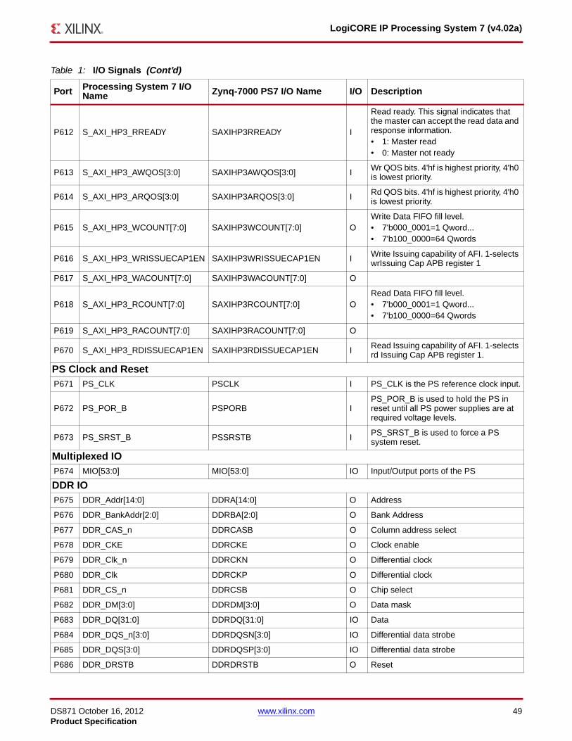
DS871 October 16, 2012 www.xilinx.com 49Product Specification
LogiCORE IP Processing System 7 (v4.02a)
P612 S_AXI_HP3_RREADY SAXIHP3RREADY I
Read ready. This signal indicates that the master can accept the read data and response information.• 1: Master read• 0: Master not ready
P613 S_AXI_HP3_AWQOS[3:0] SAXIHP3AWQOS[3:0] I Wr QOS bits. 4'hf is highest priority, 4'h0 is lowest priority.
P614 S_AXI_HP3_ARQOS[3:0] SAXIHP3ARQOS[3:0] I Rd QOS bits. 4'hf is highest priority, 4'h0 is lowest priority.
P615 S_AXI_HP3_WCOUNT[7:0] SAXIHP3WCOUNT[7:0] OWrite Data FIFO fill level.• 7'b000_0001=1 Qword...• 7'b100_0000=64 Qwords
P616 S_AXI_HP3_WRISSUECAP1EN SAXIHP3WRISSUECAP1EN I Write Issuing capability of AFI. 1-selects wrIssuing Cap APB register 1
P617 S_AXI_HP3_WACOUNT[7:0] SAXIHP3WACOUNT[7:0] O
P618 S_AXI_HP3_RCOUNT[7:0] SAXIHP3RCOUNT[7:0] ORead Data FIFO fill level.• 7'b000_0001=1 Qword...• 7'b100_0000=64 Qwords
P619 S_AXI_HP3_RACOUNT[7:0] SAXIHP3RACOUNT[7:0] O
P670 S_AXI_HP3_RDISSUECAP1EN SAXIHP3RDISSUECAP1EN I Read Issuing capability of AFI. 1-selects rd Issuing Cap APB register 1.
PS Clock and ResetP671 PS_CLK PSCLK I PS_CLK is the PS reference clock input.
P672 PS_POR_B PSPORB IPS_POR_B is used to hold the PS in reset until all PS power supplies are at required voltage levels.
P673 PS_SRST_B PSSRSTB I PS_SRST_B is used to force a PS system reset.
Multiplexed IOP674 MIO[53:0] MIO[53:0] IO Input/Output ports of the PS
DDR IOP675 DDR_Addr[14:0] DDRA[14:0] O Address
P676 DDR_BankAddr[2:0] DDRBA[2:0] O Bank Address
P677 DDR_CAS_n DDRCASB O Column address select
P678 DDR_CKE DDRCKE O Clock enable
P679 DDR_Clk_n DDRCKN O Differential clock
P680 DDR_Clk DDRCKP O Differential clock
P681 DDR_CS_n DDRCSB O Chip select
P682 DDR_DM[3:0] DDRDM[3:0] O Data mask
P683 DDR_DQ[31:0] DDRDQ[31:0] IO Data
P684 DDR_DQS_n[3:0] DDRDQSN[3:0] IO Differential data strobe
P685 DDR_DQS[3:0] DDRDQSP[3:0] IO Differential data strobe
P686 DDR_DRSTB DDRDRSTB O Reset
Table 1: I/O Signals (Cont’d)
Port Processing System 7 I/O Name Zynq-7000 PS7 I/O Name I/O Description
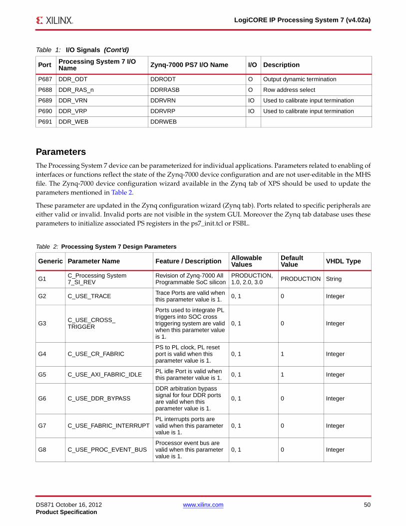
DS871 October 16, 2012 www.xilinx.com 50Product Specification
LogiCORE IP Processing System 7 (v4.02a)
ParametersThe Processing System 7 device can be parameterized for individual applications. Parameters related to enabling ofinterfaces or functions reflect the state of the Zynq-7000 device configuration and are not user-editable in the MHSfile. The Zynq-7000 device configuration wizard available in the Zynq tab of XPS should be used to update theparameters mentioned in Table 2.
These parameter are updated in the Zynq configuration wizard (Zynq tab). Ports related to specific peripherals areeither valid or invalid. Invalid ports are not visible in the system GUI. Moreover the Zynq tab database uses theseparameters to initialize associated PS registers in the ps7_init.tcl or FSBL.
P687 DDR_ODT DDRODT O Output dynamic termination
P688 DDR_RAS_n DDRRASB O Row address select
P689 DDR_VRN DDRVRN IO Used to calibrate input termination
P690 DDR_VRP DDRVRP IO Used to calibrate input termination
P691 DDR_WEB DDRWEB
Table 2: Processing System 7 Design Parameters
Generic Parameter Name Feature / Description Allowable Values
Default Value VHDL Type
G1 C_Processing System 7_SI_REV
Revision of Zynq-7000 All Programmable SoC silicon
PRODUCTION, 1.0, 2.0, 3.0 PRODUCTION String
G2 C_USE_TRACE Trace Ports are valid when this parameter value is 1. 0, 1 0 Integer
G3 C_USE_CROSS_TRIGGER
Ports used to integrate PL triggers into SOC cross triggering system are valid when this parameter value is 1.
0, 1 0 Integer
G4 C_USE_CR_FABRICPS to PL clock, PL reset port is valid when this parameter value is 1.
0, 1 1 Integer
G5 C_USE_AXI_FABRIC_IDLE PL idle Port is valid when this parameter value is 1. 0, 1 1 Integer
G6 C_USE_DDR_BYPASS
DDR arbitration bypass signal for four DDR ports are valid when this parameter value is 1.
0, 1 0 Integer
G7 C_USE_FABRIC_INTERRUPTPL interrupts ports are valid when this parameter value is 1.
0, 1 0 Integer
G8 C_USE_PROC_EVENT_BUSProcessor event bus are valid when this parameter value is 1.
0, 1 0 Integer
Table 1: I/O Signals (Cont’d)
Port Processing System 7 I/O Name Zynq-7000 PS7 I/O Name I/O Description
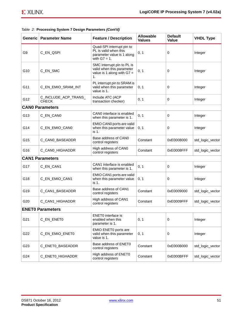
DS871 October 16, 2012 www.xilinx.com 51Product Specification
LogiCORE IP Processing System 7 (v4.02a)
G9 C_EN_QSPI
Quad-SPI interrupt pin to PL is valid when this parameter value is 1 along with G7 = 1.
0, 1 0 Integer
G10 C_EN_SMC
SMC interrupt pin to PL is valid when this parameter value is 1 along with G7 = 1.
0, 1 0 Integer
G11 C_EN_EMIO_SRAM_INTPL interrupt pin to SRAM is valid when this parameter value is 1.
0, 1 0 Integer
G12 C_INCLUDE_ACP_TRANS_CHECK
Include ATC (ACP transaction checker) 0, 1 0 Integer
CAN0 Parameters
G13 C_EN_CAN0 CAN0 interface is enabled when this parameter is 1. 0, 1 0 Integer
G14 C_EN_EMIO_CAN0EMIO CAN0 ports are valid when this parameter value is 1.
0, 1 0 Integer
G15 C_CAN0_BASEADDR Base address of CAN0 control registers Constant 0xE0008000 std_logic_vector
G16 C_CAN0_HIGHADDR High address of CAN0 control registers Constant 0xE0008FFF std_logic_vector
CAN1 Parameters
G17 C_EN_CAN1 CAN1 interface is enabled when this parameter is 1. 0, 1 0 Integer
G18 C_EN_EMIO_CAN1EMIO CAN1 ports are valid when this parameter value is 1.
0, 1 0 Integer
G19 C_CAN1_BASEADDR Base address of CAN1 control registers Constant 0xE0009000 std_logic_vector
G20 C_CAN1_HIGHADDR High address of CAN1 control registers Constant 0xE0009FFF std_logic_vector
ENET0 Parameters
G21 C_EN_ENET0ENET0 interface is enabled when this parameter is 1.
0, 1 0 Integer
G22 C_EN_EMIO_ENET0EMIO ENET0 ports are valid when this parameter value is 1.
0, 1 0 Integer
G23 C_ENET0_BASEADDR Base address of ENET0 control registers Constant 0xE000B000 std_logic_vector
G24 C_ENET0_HIGHADDR High address of ENET0 control registers Constant 0xE000BFFF std_logic_vector
Table 2: Processing System 7 Design Parameters (Cont’d)
Generic Parameter Name Feature / Description Allowable Values
Default Value VHDL Type
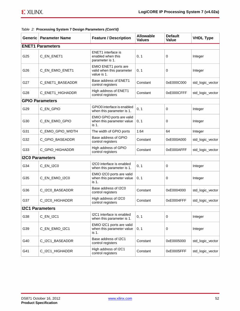
DS871 October 16, 2012 www.xilinx.com 52Product Specification
LogiCORE IP Processing System 7 (v4.02a)
ENET1 Parameters
G25 C_EN_ENET1ENET1 interface is enabled when this parameter is 1.
0, 1 0 Integer
G26 C_EN_EMIO_ENET1EMIO ENET1 ports are valid when this parameter value is 1.
0, 1 0 Integer
G27 C_ENET1_BASEADDR Base address of ENET1 control registers Constant 0xE000C000 std_logic_vector
G28 C_ENET1_HIGHADDR High address of ENET1 control registers Constant 0xE000CFFF std_logic_vector
GPIO Parameters
G29 C_EN_GPIO GPIO0 interface is enabled when this parameter is 1. 0, 1 0 Integer
G30 C_EN_EMIO_GPIOEMIO GPIO ports are valid when this parameter value is 1.
0, 1 0 Integer
G31 C_EMIO_GPIO_WIDTH The width of GPIO ports 1:64 64 Integer
G32 C_GPIO_BASEADDR Base address of GPIO control registers Constant 0xE000A000 std_logic_vector
G33 C_GPIO_HIGHADDR High address of GPIO control registers Constant 0xE000AFFF std_logic_vector
I2C0 Parameters
G34 C_EN_I2C0 I2C0 interface is enabled when this parameter is 1. 0, 1 0 Integer
G35 C_EN_EMIO_I2C0EMIO I2C0 ports are valid when this parameter value is 1.
0, 1 0 Integer
G36 C_I2C0_BASEADDR Base address of I2C0 control registers Constant 0xE0004000 std_logic_vector
G37 C_I2C0_HIGHADDR High address of I2C0 control registers Constant 0xE0004FFF std_logic_vector
I2C1 Parameters
G38 C_EN_I2C1 I2C1 interface is enabled when this parameter is 1. 0, 1 0 Integer
G39 C_EN_EMIO_I2C1EMIO I2C1 ports are valid when this parameter value is 1.
0, 1 0 Integer
G40 C_I2C1_BASEADDR Base address of I2C1 control registers Constant 0xE0005000 std_logic_vector
G41 C_I2C1_HIGHADDR High address of I2C1 control registers Constant 0xE0005FFF std_logic_vector
Table 2: Processing System 7 Design Parameters (Cont’d)
Generic Parameter Name Feature / Description Allowable Values
Default Value VHDL Type
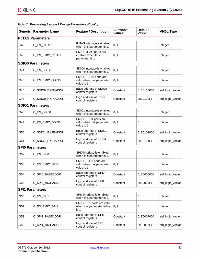
DS871 October 16, 2012 www.xilinx.com 53Product Specification
LogiCORE IP Processing System 7 (v4.02a)
PJTAG Parameters
G42 C_EN_PJTAG PJTAG interface is enabled when this parameter is 1. 0, 1 0 Integer
G43 C_EN_EMIO_PJTAGEMIO PJTAG ports are enabled when this parameter is 1.
0, 1 0 Integer
SDIO0 Parameters
G44 C_EN_SDIO0 SDIO0 interface is enabled when this parameter is 1. 0, 1 0 Integer
G45 C_EN_EMIO_SDIO0EMIO SDIO 0 ports are valid when this parameter value is 1.
0, 1 0 Integer
G46 C_SDIO0_BASEADDR Base address of SDIO0 control registers Constant 0xE0100000 std_logic_vector
G47 C_SDIO0_HIGHADDR High address of SDIO0 control registers Constant 0xE0100FFF std_logic_vector
SDIO1 Parameters
G48 C_EN_SDIO1 SDIO1 interface is enabled when this parameter is 1. 0, 1 0 Integer
G49 C_EN_EMIO_SDIO1EMIO SDIO1 ports are valid when this parameter value is 1.
0, 1 0 Integer
G50 C_SDIO1_BASEADDR Base address of SDIO1 control registers Constant 0xE0101000 std_logic_vector
G51 C_SDIO1_HIGHADDR High address of SDIO1 control registers Constant 0xE0101FFF std_logic_vector
SPI0 Parameters
G52 C_EN_SPI0 SPI0 interface is enabled when this parameter is 1. 0, 1 0 Integer
G53 C_EN_EMIO_SPI0EMIO SPIO0 ports are valid when this parameter value is 1.
0, 1 0 Integer
G54 C_SPI0_BASEADDR Base address of SPI0 control registers Constant 0xE0006000 std_logic_vector
G55 C_SPI0_HIGHADDR High address of SPI0 control registers Constant 0xE0006FFF std_logic_vector
SPI1 Parameters
G56 C_EN_SPI1 SPI1 interface is enabled when this parameter is 1. 0, 1 0 Integer
G57 C_EN_EMIO_SPI1EMIO SPI1 ports are valid when this parameter value is 1.
0, 1 0 Integer
G58 C_SPI1_BASEADDR Base address of SPI1 control registers Constant 0xE0007000 std_logic_vector
G59 C_SPI1_HIGHADDR High address of SPI1 control registers Constant 0xE0007FFF std_logic_vector
Table 2: Processing System 7 Design Parameters (Cont’d)
Generic Parameter Name Feature / Description Allowable Values
Default Value VHDL Type
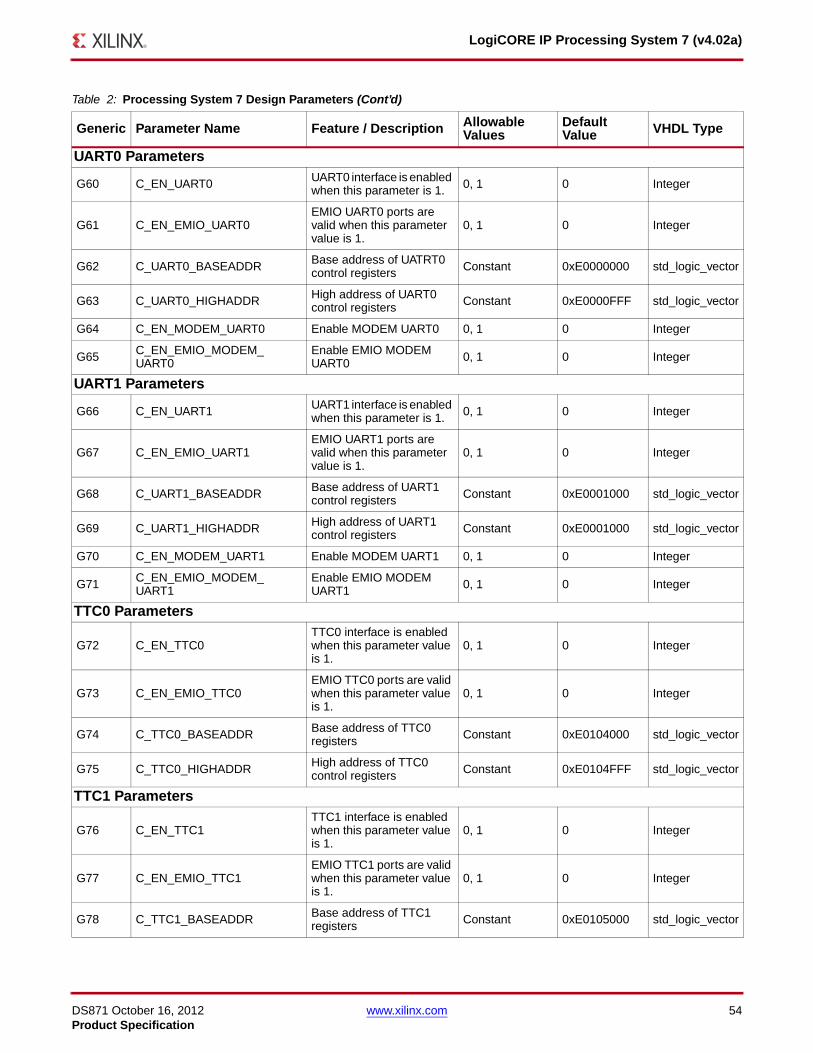
DS871 October 16, 2012 www.xilinx.com 54Product Specification
LogiCORE IP Processing System 7 (v4.02a)
UART0 Parameters
G60 C_EN_UART0 UART0 interface is enabled when this parameter is 1. 0, 1 0 Integer
G61 C_EN_EMIO_UART0EMIO UART0 ports are valid when this parameter value is 1.
0, 1 0 Integer
G62 C_UART0_BASEADDR Base address of UATRT0 control registers Constant 0xE0000000 std_logic_vector
G63 C_UART0_HIGHADDR High address of UART0 control registers Constant 0xE0000FFF std_logic_vector
G64 C_EN_MODEM_UART0 Enable MODEM UART0 0, 1 0 Integer
G65 C_EN_EMIO_MODEM_UART0
Enable EMIO MODEM UART0 0, 1 0 Integer
UART1 Parameters
G66 C_EN_UART1 UART1 interface is enabled when this parameter is 1. 0, 1 0 Integer
G67 C_EN_EMIO_UART1EMIO UART1 ports are valid when this parameter value is 1.
0, 1 0 Integer
G68 C_UART1_BASEADDR Base address of UART1 control registers Constant 0xE0001000 std_logic_vector
G69 C_UART1_HIGHADDR High address of UART1 control registers Constant 0xE0001000 std_logic_vector
G70 C_EN_MODEM_UART1 Enable MODEM UART1 0, 1 0 Integer
G71 C_EN_EMIO_MODEM_UART1
Enable EMIO MODEM UART1 0, 1 0 Integer
TTC0 Parameters
G72 C_EN_TTC0TTC0 interface is enabled when this parameter value is 1.
0, 1 0 Integer
G73 C_EN_EMIO_TTC0EMIO TTC0 ports are valid when this parameter value is 1.
0, 1 0 Integer
G74 C_TTC0_BASEADDR Base address of TTC0 registers Constant 0xE0104000 std_logic_vector
G75 C_TTC0_HIGHADDR High address of TTC0 control registers Constant 0xE0104FFF std_logic_vector
TTC1 Parameters
G76 C_EN_TTC1TTC1 interface is enabled when this parameter value is 1.
0, 1 0 Integer
G77 C_EN_EMIO_TTC1EMIO TTC1 ports are valid when this parameter value is 1.
0, 1 0 Integer
G78 C_TTC1_BASEADDR Base address of TTC1 registers Constant 0xE0105000 std_logic_vector
Table 2: Processing System 7 Design Parameters (Cont’d)
Generic Parameter Name Feature / Description Allowable Values
Default Value VHDL Type
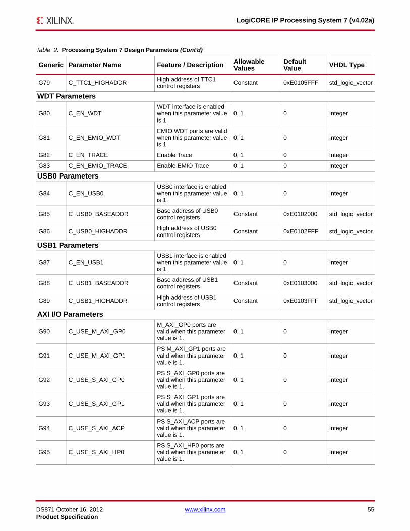
DS871 October 16, 2012 www.xilinx.com 55Product Specification
LogiCORE IP Processing System 7 (v4.02a)
G79 C_TTC1_HIGHADDR High address of TTC1 control registers Constant 0xE0105FFF std_logic_vector
WDT Parameters
G80 C_EN_WDTWDT interface is enabled when this parameter value is 1.
0, 1 0 Integer
G81 C_EN_EMIO_WDTEMIO WDT ports are valid when this parameter value is 1.
0, 1 0 Integer
G82 C_EN_TRACE Enable Trace 0, 1 0 Integer
G83 C_EN_EMIO_TRACE Enable EMIO Trace 0, 1 0 Integer
USB0 Parameters
G84 C_EN_USB0USB0 interface is enabled when this parameter value is 1.
0, 1 0 Integer
G85 C_USB0_BASEADDR Base address of USB0 control registers Constant 0xE0102000 std_logic_vector
G86 C_USB0_HIGHADDR High address of USB0 control registers Constant 0xE0102FFF std_logic_vector
USB1 Parameters
G87 C_EN_USB1USB1 interface is enabled when this parameter value is 1.
0, 1 0 Integer
G88 C_USB1_BASEADDR Base address of USB1 control registers Constant 0xE0103000 std_logic_vector
G89 C_USB1_HIGHADDR High address of USB1 control registers Constant 0xE0103FFF std_logic_vector
AXI I/O Parameters
G90 C_USE_M_AXI_GP0M_AXI_GP0 ports are valid when this parameter value is 1.
0, 1 0 Integer
G91 C_USE_M_AXI_GP1PS M_AXI_GP1 ports are valid when this parameter value is 1.
0, 1 0 Integer
G92 C_USE_S_AXI_GP0PS S_AXI_GP0 ports are valid when this parameter value is 1.
0, 1 0 Integer
G93 C_USE_S_AXI_GP1PS S_AXI_GP1 ports are valid when this parameter value is 1.
0, 1 0 Integer
G94 C_USE_S_AXI_ACPPS S_AXI_ACP ports are valid when this parameter value is 1.
0, 1 0 Integer
G95 C_USE_S_AXI_HP0PS S_AXI_HP0 ports are valid when this parameter value is 1.
0, 1 0 Integer
Table 2: Processing System 7 Design Parameters (Cont’d)
Generic Parameter Name Feature / Description Allowable Values
Default Value VHDL Type
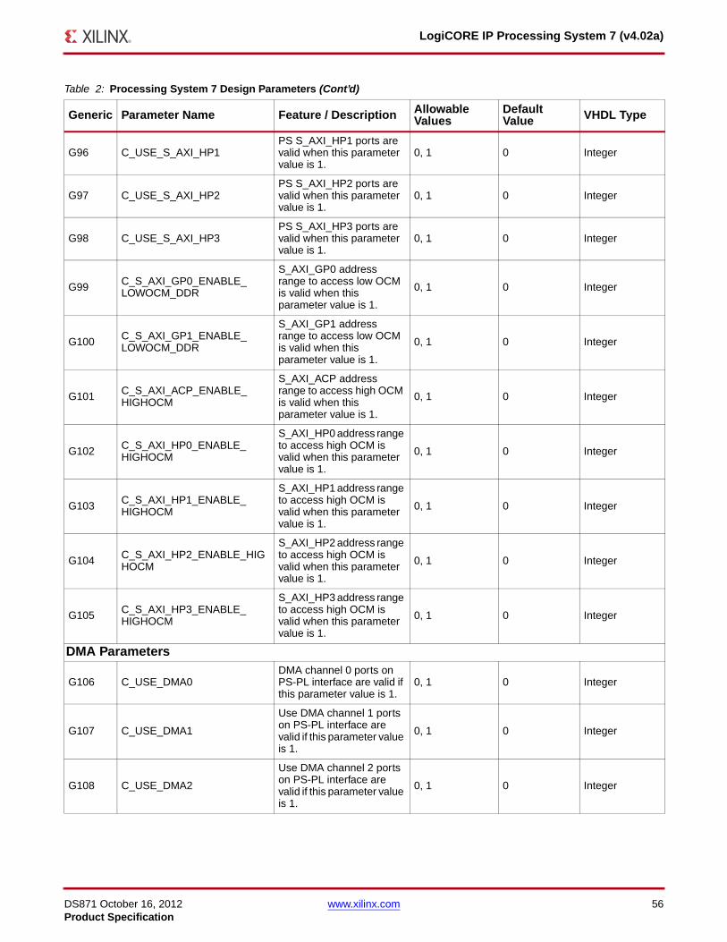
DS871 October 16, 2012 www.xilinx.com 56Product Specification
LogiCORE IP Processing System 7 (v4.02a)
G96 C_USE_S_AXI_HP1PS S_AXI_HP1 ports are valid when this parameter value is 1.
0, 1 0 Integer
G97 C_USE_S_AXI_HP2PS S_AXI_HP2 ports are valid when this parameter value is 1.
0, 1 0 Integer
G98 C_USE_S_AXI_HP3PS S_AXI_HP3 ports are valid when this parameter value is 1.
0, 1 0 Integer
G99 C_S_AXI_GP0_ENABLE_LOWOCM_DDR
S_AXI_GP0 address range to access low OCM is valid when this parameter value is 1.
0, 1 0 Integer
G100 C_S_AXI_GP1_ENABLE_LOWOCM_DDR
S_AXI_GP1 address range to access low OCM is valid when this parameter value is 1.
0, 1 0 Integer
G101 C_S_AXI_ACP_ENABLE_HIGHOCM
S_AXI_ACP address range to access high OCM is valid when this parameter value is 1.
0, 1 0 Integer
G102 C_S_AXI_HP0_ENABLE_HIGHOCM
S_AXI_HP0 address range to access high OCM is valid when this parameter value is 1.
0, 1 0 Integer
G103 C_S_AXI_HP1_ENABLE_HIGHOCM
S_AXI_HP1 address range to access high OCM is valid when this parameter value is 1.
0, 1 0 Integer
G104 C_S_AXI_HP2_ENABLE_HIGHOCM
S_AXI_HP2 address range to access high OCM is valid when this parameter value is 1.
0, 1 0 Integer
G105 C_S_AXI_HP3_ENABLE_HIGHOCM
S_AXI_HP3 address range to access high OCM is valid when this parameter value is 1.
0, 1 0 Integer
DMA Parameters
G106 C_USE_DMA0DMA channel 0 ports on PS-PL interface are valid if this parameter value is 1.
0, 1 0 Integer
G107 C_USE_DMA1
Use DMA channel 1 ports on PS-PL interface are valid if this parameter value is 1.
0, 1 0 Integer
G108 C_USE_DMA2
Use DMA channel 2 ports on PS-PL interface are valid if this parameter value is 1.
0, 1 0 Integer
Table 2: Processing System 7 Design Parameters (Cont’d)
Generic Parameter Name Feature / Description Allowable Values
Default Value VHDL Type
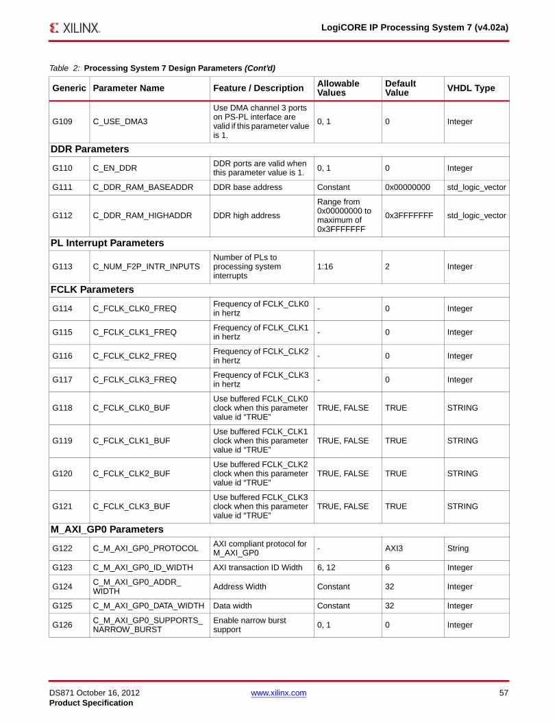
DS871 October 16, 2012 www.xilinx.com 57Product Specification
LogiCORE IP Processing System 7 (v4.02a)
G109 C_USE_DMA3
Use DMA channel 3 ports on PS-PL interface are valid if this parameter value is 1.
0, 1 0 Integer
DDR Parameters
G110 C_EN_DDR DDR ports are valid when this parameter value is 1. 0, 1 0 Integer
G111 C_DDR_RAM_BASEADDR DDR base address Constant 0x00000000 std_logic_vector
G112 C_DDR_RAM_HIGHADDR DDR high address
Range from 0x00000000 to maximum of 0x3FFFFFFF
0x3FFFFFFF std_logic_vector
PL Interrupt Parameters
G113 C_NUM_F2P_INTR_INPUTSNumber of PLs to processing system interrupts
1:16 2 Integer
FCLK Parameters
G114 C_FCLK_CLK0_FREQ Frequency of FCLK_CLK0 in hertz - 0 Integer
G115 C_FCLK_CLK1_FREQ Frequency of FCLK_CLK1 in hertz - 0 Integer
G116 C_FCLK_CLK2_FREQ Frequency of FCLK_CLK2 in hertz - 0 Integer
G117 C_FCLK_CLK3_FREQ Frequency of FCLK_CLK3 in hertz - 0 Integer
G118 C_FCLK_CLK0_BUFUse buffered FCLK_CLK0 clock when this parameter value id “TRUE”
TRUE, FALSE TRUE STRING
G119 C_FCLK_CLK1_BUFUse buffered FCLK_CLK1 clock when this parameter value id “TRUE”
TRUE, FALSE TRUE STRING
G120 C_FCLK_CLK2_BUFUse buffered FCLK_CLK2 clock when this parameter value id “TRUE”
TRUE, FALSE TRUE STRING
G121 C_FCLK_CLK3_BUFUse buffered FCLK_CLK3 clock when this parameter value id “TRUE”
TRUE, FALSE TRUE STRING
M_AXI_GP0 Parameters
G122 C_M_AXI_GP0_PROTOCOL AXI compliant protocol for M_AXI_GP0 - AXI3 String
G123 C_M_AXI_GP0_ID_WIDTH AXI transaction ID Width 6, 12 6 Integer
G124 C_M_AXI_GP0_ADDR_WIDTH Address Width Constant 32 Integer
G125 C_M_AXI_GP0_DATA_WIDTH Data width Constant 32 Integer
G126 C_M_AXI_GP0_SUPPORTS_NARROW_BURST
Enable narrow burst support 0, 1 0 Integer
Table 2: Processing System 7 Design Parameters (Cont’d)
Generic Parameter Name Feature / Description Allowable Values
Default Value VHDL Type
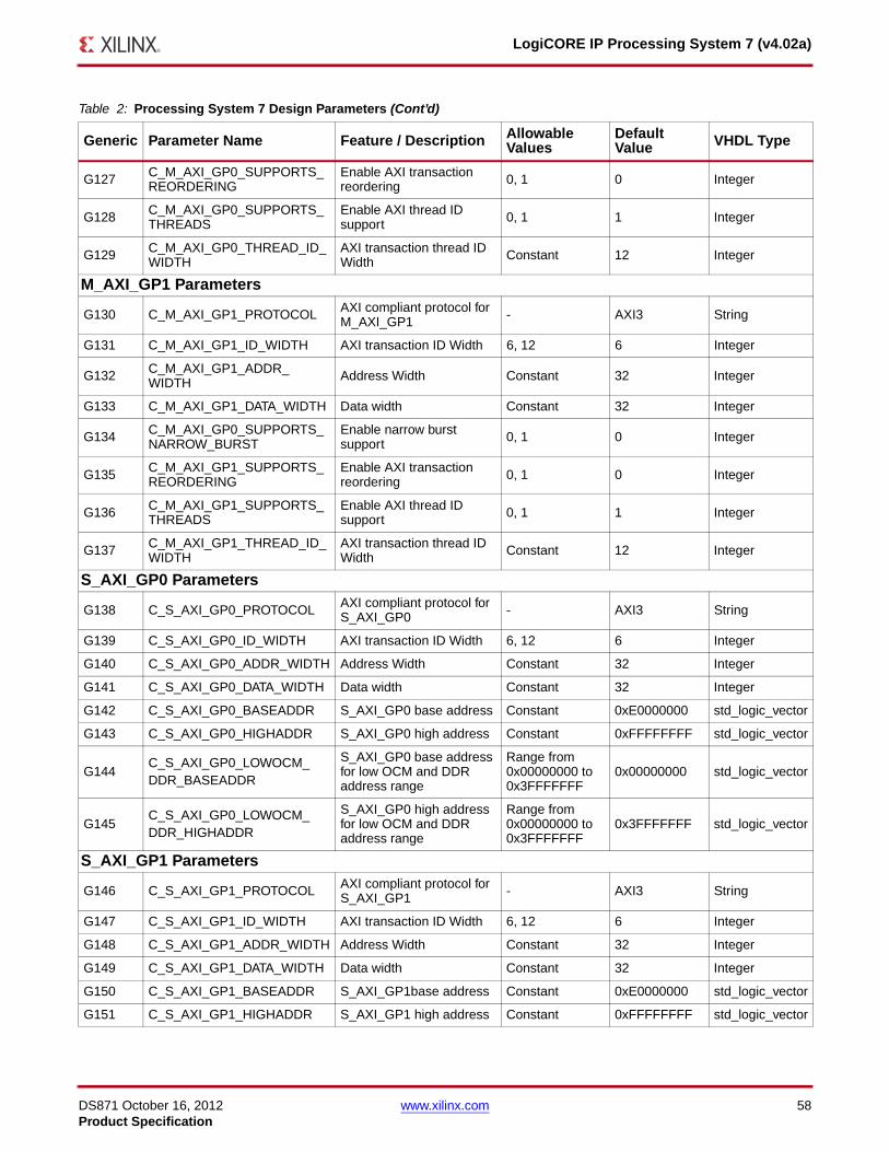
DS871 October 16, 2012 www.xilinx.com 58Product Specification
LogiCORE IP Processing System 7 (v4.02a)
G127 C_M_AXI_GP0_SUPPORTS_REORDERING
Enable AXI transaction reordering 0, 1 0 Integer
G128 C_M_AXI_GP0_SUPPORTS_THREADS
Enable AXI thread ID support 0, 1 1 Integer
G129 C_M_AXI_GP0_THREAD_ID_WIDTH
AXI transaction thread ID Width Constant 12 Integer
M_AXI_GP1 Parameters
G130 C_M_AXI_GP1_PROTOCOL AXI compliant protocol for M_AXI_GP1 - AXI3 String
G131 C_M_AXI_GP1_ID_WIDTH AXI transaction ID Width 6, 12 6 Integer
G132 C_M_AXI_GP1_ADDR_WIDTH Address Width Constant 32 Integer
G133 C_M_AXI_GP1_DATA_WIDTH Data width Constant 32 Integer
G134 C_M_AXI_GP0_SUPPORTS_NARROW_BURST
Enable narrow burst support 0, 1 0 Integer
G135 C_M_AXI_GP1_SUPPORTS_REORDERING
Enable AXI transaction reordering 0, 1 0 Integer
G136 C_M_AXI_GP1_SUPPORTS_THREADS
Enable AXI thread ID support 0, 1 1 Integer
G137 C_M_AXI_GP1_THREAD_ID_WIDTH
AXI transaction thread ID Width Constant 12 Integer
S_AXI_GP0 Parameters
G138 C_S_AXI_GP0_PROTOCOL AXI compliant protocol for S_AXI_GP0 - AXI3 String
G139 C_S_AXI_GP0_ID_WIDTH AXI transaction ID Width 6, 12 6 Integer
G140 C_S_AXI_GP0_ADDR_WIDTH Address Width Constant 32 Integer
G141 C_S_AXI_GP0_DATA_WIDTH Data width Constant 32 Integer
G142 C_S_AXI_GP0_BASEADDR S_AXI_GP0 base address Constant 0xE0000000 std_logic_vector
G143 C_S_AXI_GP0_HIGHADDR S_AXI_GP0 high address Constant 0xFFFFFFFF std_logic_vector
G144C_S_AXI_GP0_LOWOCM_DDR_BASEADDR
S_AXI_GP0 base address for low OCM and DDR address range
Range from 0x00000000 to 0x3FFFFFFF
0x00000000 std_logic_vector
G145C_S_AXI_GP0_LOWOCM_DDR_HIGHADDR
S_AXI_GP0 high address for low OCM and DDR address range
Range from 0x00000000 to 0x3FFFFFFF
0x3FFFFFFF std_logic_vector
S_AXI_GP1 Parameters
G146 C_S_AXI_GP1_PROTOCOL AXI compliant protocol for S_AXI_GP1 - AXI3 String
G147 C_S_AXI_GP1_ID_WIDTH AXI transaction ID Width 6, 12 6 Integer
G148 C_S_AXI_GP1_ADDR_WIDTH Address Width Constant 32 Integer
G149 C_S_AXI_GP1_DATA_WIDTH Data width Constant 32 Integer
G150 C_S_AXI_GP1_BASEADDR S_AXI_GP1base address Constant 0xE0000000 std_logic_vector
G151 C_S_AXI_GP1_HIGHADDR S_AXI_GP1 high address Constant 0xFFFFFFFF std_logic_vector
Table 2: Processing System 7 Design Parameters (Cont’d)
Generic Parameter Name Feature / Description Allowable Values
Default Value VHDL Type
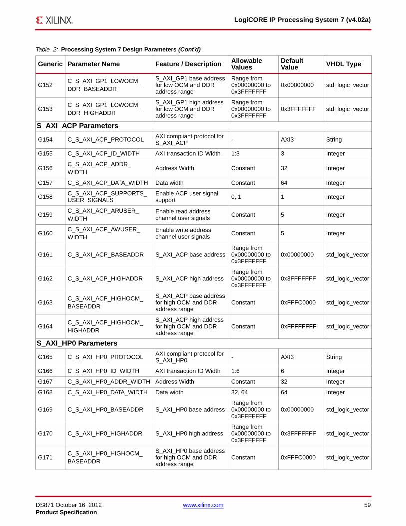
DS871 October 16, 2012 www.xilinx.com 59Product Specification
LogiCORE IP Processing System 7 (v4.02a)
G152C_S_AXI_GP1_LOWOCM_DDR_BASEADDR
S_AXI_GP1 base address for low OCM and DDR address range
Range from 0x00000000 to 0x3FFFFFFF
0x00000000 std_logic_vector
G153C_S_AXI_GP1_LOWOCM_DDR_HIGHADDR
S_AXI_GP1 high address for low OCM and DDR address range
Range from 0x00000000 to 0x3FFFFFFF
0x3FFFFFFF std_logic_vector
S_AXI_ACP Parameters
G154 C_S_AXI_ACP_PROTOCOL AXI compliant protocol for S_AXI_ACP - AXI3 String
G155 C_S_AXI_ACP_ID_WIDTH AXI transaction ID Width 1:3 3 Integer
G156C_S_AXI_ACP_ADDR_WIDTH
Address Width Constant 32 Integer
G157 C_S_AXI_ACP_DATA_WIDTH Data width Constant 64 Integer
G158 C_S_AXI_ACP_SUPPORTS_USER_SIGNALS
Enable ACP user signal support 0, 1 1 Integer
G159C_S_AXI_ACP_ARUSER_WIDTH
Enable read address channel user signals Constant 5 Integer
G160C_S_AXI_ACP_AWUSER_WIDTH
Enable write address channel user signals Constant 5 Integer
G161 C_S_AXI_ACP_BASEADDR S_AXI_ACP base addressRange from 0x00000000 to 0x3FFFFFFF
0x00000000 std_logic_vector
G162 C_S_AXI_ACP_HIGHADDR S_AXI_ACP high addressRange from 0x00000000 to 0x3FFFFFFF
0x3FFFFFFF std_logic_vector
G163C_S_AXI_ACP_HIGHOCM_BASEADDR
S_AXI_ACP base address for high OCM and DDR address range
Constant 0xFFFC0000 std_logic_vector
G164C_S_AXI_ACP_HIGHOCM_HIGHADDR
S_AXI_ACP high address for high OCM and DDR address range
Constant 0xFFFFFFFF std_logic_vector
S_AXI_HP0 Parameters
G165 C_S_AXI_HP0_PROTOCOL AXI compliant protocol for S_AXI_HP0 - AXI3 String
G166 C_S_AXI_HP0_ID_WIDTH AXI transaction ID Width 1:6 6 Integer
G167 C_S_AXI_HP0_ADDR_WIDTH Address Width Constant 32 Integer
G168 C_S_AXI_HP0_DATA_WIDTH Data width 32, 64 64 Integer
G169 C_S_AXI_HP0_BASEADDR S_AXI_HP0 base addressRange from 0x00000000 to 0x3FFFFFFF
0x00000000 std_logic_vector
G170 C_S_AXI_HP0_HIGHADDR S_AXI_HP0 high addressRange from 0x00000000 to 0x3FFFFFFF
0x3FFFFFFF std_logic_vector
G171C_S_AXI_HP0_HIGHOCM_BASEADDR
S_AXI_HP0 base address for high OCM and DDR address range
Constant 0xFFFC0000 std_logic_vector
Table 2: Processing System 7 Design Parameters (Cont’d)
Generic Parameter Name Feature / Description Allowable Values
Default Value VHDL Type
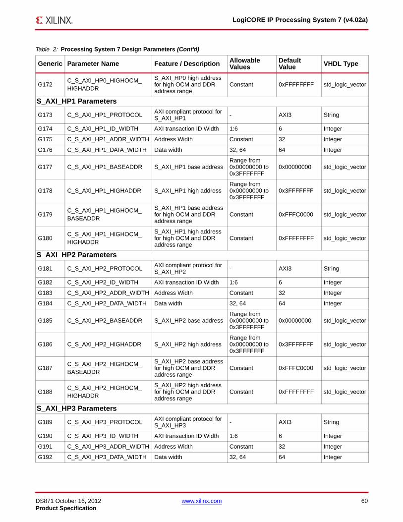
DS871 October 16, 2012 www.xilinx.com 60Product Specification
LogiCORE IP Processing System 7 (v4.02a)
G172C_S_AXI_HP0_HIGHOCM_HIGHADDR
S_AXI_HP0 high address for high OCM and DDR address range
Constant 0xFFFFFFFF std_logic_vector
S_AXI_HP1 Parameters
G173 C_S_AXI_HP1_PROTOCOL AXI compliant protocol for S_AXI_HP1 - AXI3 String
G174 C_S_AXI_HP1_ID_WIDTH AXI transaction ID Width 1:6 6 Integer
G175 C_S_AXI_HP1_ADDR_WIDTH Address Width Constant 32 Integer
G176 C_S_AXI_HP1_DATA_WIDTH Data width 32, 64 64 Integer
G177 C_S_AXI_HP1_BASEADDR S_AXI_HP1 base addressRange from 0x00000000 to 0x3FFFFFFF
0x00000000 std_logic_vector
G178 C_S_AXI_HP1_HIGHADDR S_AXI_HP1 high addressRange from 0x00000000 to 0x3FFFFFFF
0x3FFFFFFF std_logic_vector
G179C_S_AXI_HP1_HIGHOCM_BASEADDR
S_AXI_HP1 base address for high OCM and DDR address range
Constant 0xFFFC0000 std_logic_vector
G180C_S_AXI_HP1_HIGHOCM_HIGHADDR
S_AXI_HP1 high address for high OCM and DDR address range
Constant 0xFFFFFFFF std_logic_vector
S_AXI_HP2 Parameters
G181 C_S_AXI_HP2_PROTOCOL AXI compliant protocol for S_AXI_HP2 - AXI3 String
G182 C_S_AXI_HP2_ID_WIDTH AXI transaction ID Width 1:6 6 Integer
G183 C_S_AXI_HP2_ADDR_WIDTH Address Width Constant 32 Integer
G184 C_S_AXI_HP2_DATA_WIDTH Data width 32, 64 64 Integer
G185 C_S_AXI_HP2_BASEADDR S_AXI_HP2 base addressRange from 0x00000000 to 0x3FFFFFFF
0x00000000 std_logic_vector
G186 C_S_AXI_HP2_HIGHADDR S_AXI_HP2 high addressRange from 0x00000000 to 0x3FFFFFFF
0x3FFFFFFF std_logic_vector
G187C_S_AXI_HP2_HIGHOCM_BASEADDR
S_AXI_HP2 base address for high OCM and DDR address range
Constant 0xFFFC0000 std_logic_vector
G188C_S_AXI_HP2_HIGHOCM_HIGHADDR
S_AXI_HP2 high address for high OCM and DDR address range
Constant 0xFFFFFFFF std_logic_vector
S_AXI_HP3 Parameters
G189 C_S_AXI_HP3_PROTOCOL AXI compliant protocol for S_AXI_HP3 - AXI3 String
G190 C_S_AXI_HP3_ID_WIDTH AXI transaction ID Width 1:6 6 Integer
G191 C_S_AXI_HP3_ADDR_WIDTH Address Width Constant 32 Integer
G192 C_S_AXI_HP3_DATA_WIDTH Data width 32, 64 64 Integer
Table 2: Processing System 7 Design Parameters (Cont’d)
Generic Parameter Name Feature / Description Allowable Values
Default Value VHDL Type
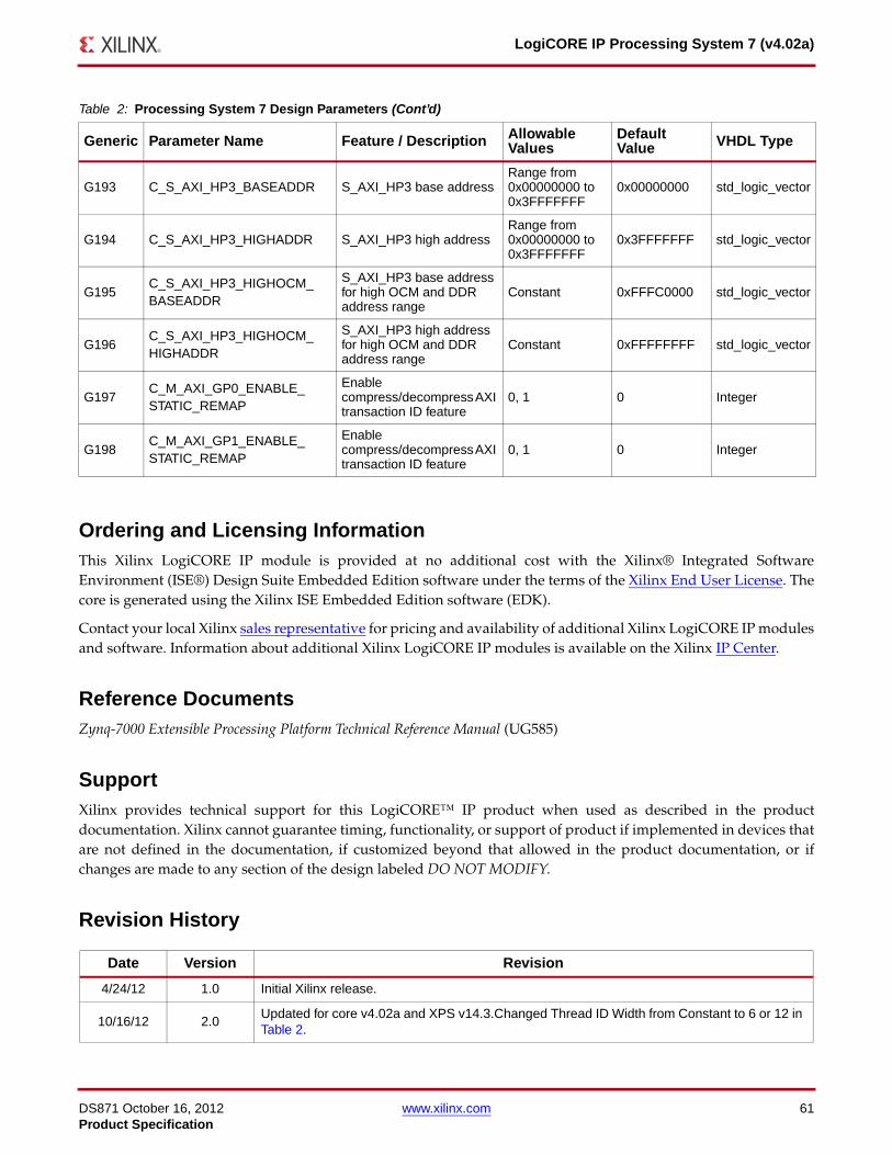
DS871 October 16, 2012 www.xilinx.com 61Product Specification
LogiCORE IP Processing System 7 (v4.02a)
Ordering and Licensing InformationThis Xilinx LogiCORE IP module is provided at no additional cost with the Xilinx® Integrated SoftwareEnvironment (ISE®) Design Suite Embedded Edition software under the terms of the Xilinx End User License. Thecore is generated using the Xilinx ISE Embedded Edition software (EDK).
Contact your local Xilinx sales representative for pricing and availability of additional Xilinx LogiCORE IP modulesand software. Information about additional Xilinx LogiCORE IP modules is available on the Xilinx IP Center.
Reference DocumentsZynq-7000 Extensible Processing Platform Technical Reference Manual (UG585)
SupportXilinx provides technical support for this LogiCORE™ IP product when used as described in the productdocumentation. Xilinx cannot guarantee timing, functionality, or support of product if implemented in devices thatare not defined in the documentation, if customized beyond that allowed in the product documentation, or ifchanges are made to any section of the design labeled DO NOT MODIFY.
Revision History
G193 C_S_AXI_HP3_BASEADDR S_AXI_HP3 base addressRange from 0x00000000 to 0x3FFFFFFF
0x00000000 std_logic_vector
G194 C_S_AXI_HP3_HIGHADDR S_AXI_HP3 high addressRange from 0x00000000 to 0x3FFFFFFF
0x3FFFFFFF std_logic_vector
G195C_S_AXI_HP3_HIGHOCM_BASEADDR
S_AXI_HP3 base address for high OCM and DDR address range
Constant 0xFFFC0000 std_logic_vector
G196C_S_AXI_HP3_HIGHOCM_HIGHADDR
S_AXI_HP3 high address for high OCM and DDR address range
Constant 0xFFFFFFFF std_logic_vector
G197C_M_AXI_GP0_ENABLE_STATIC_REMAP
Enable compress/decompress AXI transaction ID feature
0, 1 0 Integer
G198C_M_AXI_GP1_ENABLE_STATIC_REMAP
Enable compress/decompress AXI transaction ID feature
0, 1 0 Integer
Date Version Revision
4/24/12 1.0 Initial Xilinx release.
10/16/12 2.0Updated for core v4.02a and XPS v14.3.Changed Thread ID Width from Constant to 6 or 12 in Table 2.
Table 2: Processing System 7 Design Parameters (Cont’d)
Generic Parameter Name Feature / Description Allowable Values
Default Value VHDL Type
DS871 October 16, 2012 www.xilinx.com 62Product Specification
LogiCORE IP Processing System 7 (v4.02a)
Notice of DisclaimerThe information disclosed to you hereunder (the “Materials”) is provided solely for the selection and use of Xilinx products. Tothe maximum extent permitted by applicable law: (1) Materials are made available “AS IS” and with all faults, Xilinx herebyDISCLAIMS ALL WARRANTIES AND CONDITIONS, EXPRESS, IMPLIED, OR STATUTORY, INCLUDING BUT NOTLIMITED TO WARRANTIES OF MERCHANTABILITY, NON-INFRINGEMENT, OR FITNESS FOR ANY PARTICULARPURPOSE; and (2) Xilinx shall not be liable (whether in contract or tort, including negligence, or under any other theory ofliability) for any loss or damage of any kind or nature related to, arising under, or in connection with, the Materials (includingyour use of the Materials), including for any direct, indirect, special, incidental, or consequential loss or damage (including lossof data, profits, goodwill, or any type of loss or damage suffered as a result of any action brought by a third party) even if suchdamage or loss was reasonably foreseeable or Xilinx had been advised of the possibility of the same. Xilinx assumes noobligation to correct any errors contained in the Materials or to notify you of updates to the Materials or to productspecifications. You may not reproduce, modify, distribute, or publicly display the Materials without prior written consent.Certain products are subject to the terms and conditions of the Limited Warranties which can be viewed athttp://www.xilinx.com/warranty.htm; IP cores may be subject to warranty and support terms contained in a license issued toyou by Xilinx. Xilinx products are not designed or intended to be fail-safe or for use in any application requiring fail-safeperformance; you assume sole risk and liability for use of Xilinx products in Critical Applications:http://www.xilinx.com/warranty.htm#critapps.