Embed Size (px)
DESCRIPTION
basic things about logic gate
Citation preview
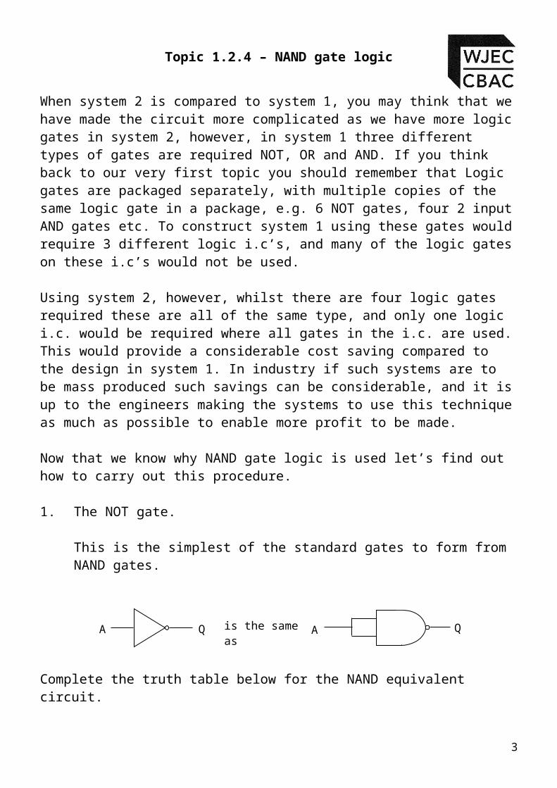
Topic 1.2.4 – NAND gate logic
Learning Objectives:
At the end of this topic you will be able to;
Use combinations of NAND gates to perform other logic functions;
Implement a logic system using only NAND gates; Recognise redundant gates in a logic system constructed only
from NAND gates.
1
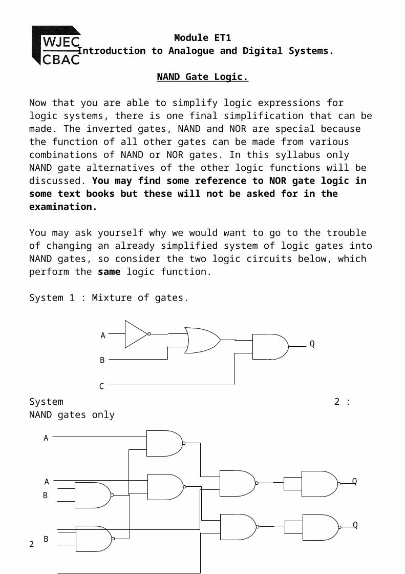
Module ET1 Introduction to Analogue and Digital Systems.
NAND Gate Logic.
Now that you are able to simplify logic expressions for logic systems, there is one final simplification that can be made. The inverted gates, NAND and NOR are special because the function of all other gates can be made from various combinations of NAND or NOR gates. In this syllabus only NAND gate alternatives of the other logic functions will be discussed. You may find some reference to NOR gate logic in some text books but these will not be asked for in the examination.
You may ask yourself why we would want to go to the trouble of changing an already simplified system of logic gates into NAND gates, so consider the two logic circuits below, which perform the same logic function.
System 1 : Mixture of gates.
System 2 : NAND gates only
When system 2 is compared to system 1, you may think that we have made the circuit more complicated as we have more logic gates in system 2, however, in system 1 three different types of gates are required NOT, OR and AND. If you think back to our very first topic you should remember that Logic gates are packaged separately, with multiple copies of the same logic gate in a package, e.g. 6 NOT gates, 2
QA
B
C
A
B
Q
A
B
Q
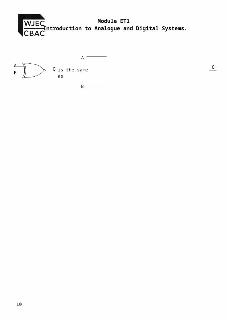
A Q A Qis the same as
Topic 1.2.4 – NAND gate logic
four 2 input AND gates etc. To construct system 1 using these gates would require 3 different logic i.c’s, and many of the logic gates on these i.c’s would not be used.
Using system 2, however, whilst there are four logic gates required these are all of the same type, and only one logic i.c. would be required where all gates in the i.c. are used. This would provide a considerable cost saving compared to the design in system 1. In industry if such systems are to be mass produced such savings can be considerable, and it is up to the engineers making the systems to use this technique as much as possible to enable more profit to be made.
Now that we know why NAND gate logic is used let’s find out how to carry out this procedure.
1. The NOT gate.
This is the simplest of the standard gates to form from NAND gates.
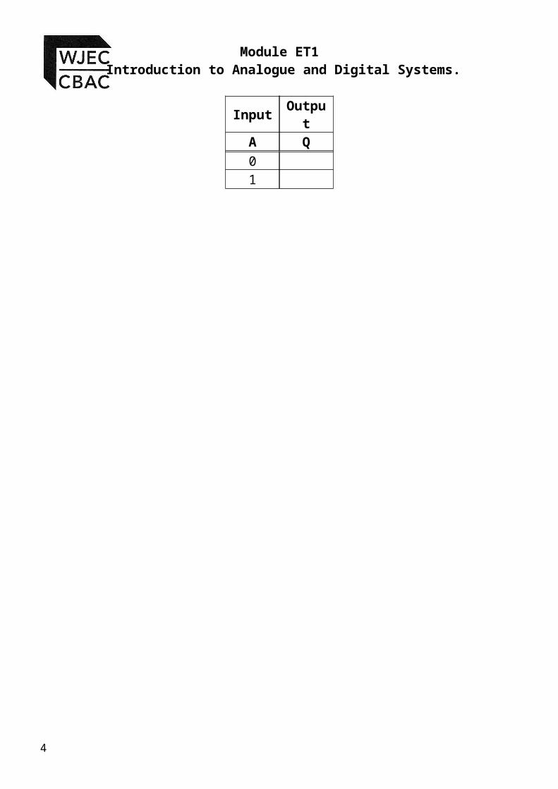
Complete the truth table below for the NAND equivalent circuit.
Input Output
A Q01
3
AAB Q
AB QX
is the same as
A
Q
B
AB
Q
XA
YA
Module ET1 Introduction to Analogue and Digital Systems.
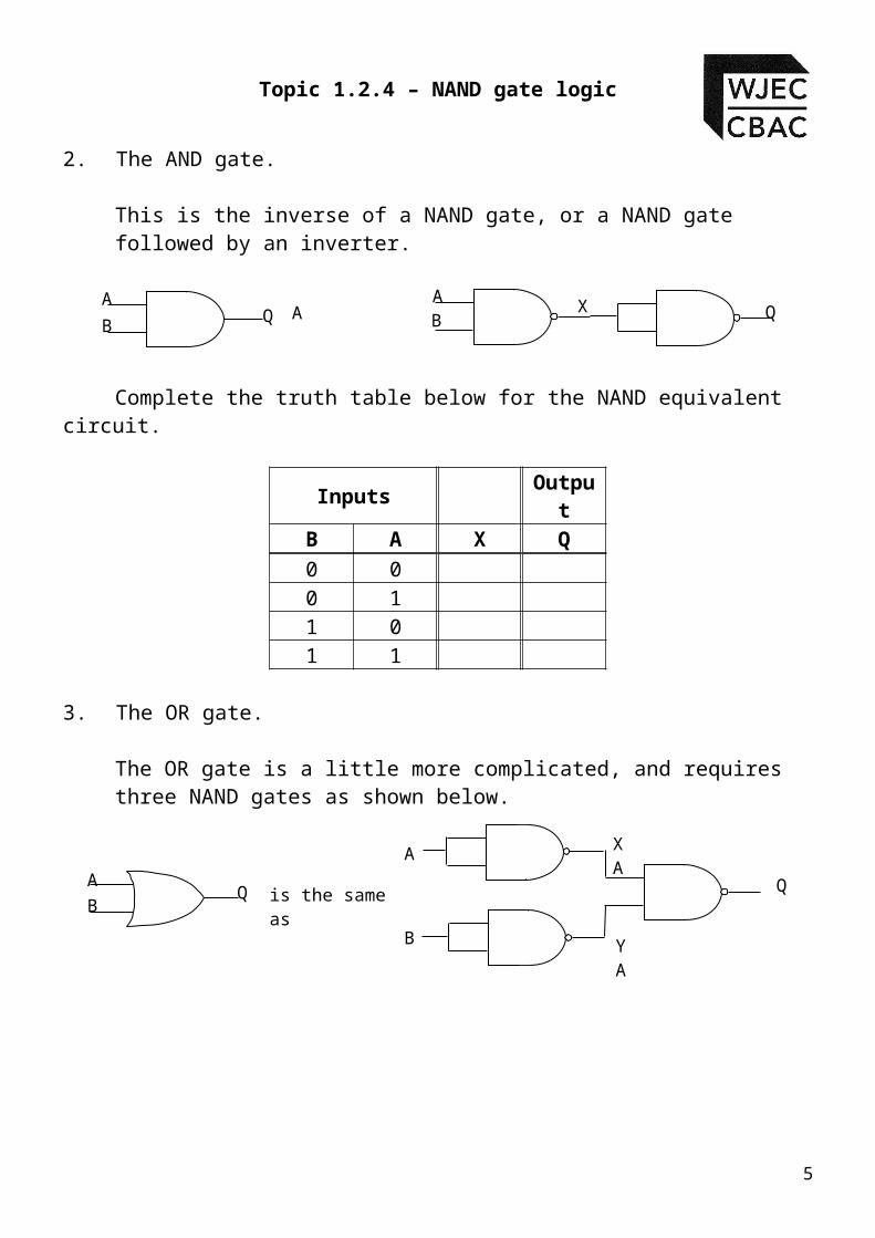
2. The AND gate.
This is the inverse of a NAND gate, or a NAND gate followed by an inverter.
Complete the truth table below for the NAND equivalent circuit.
Inputs Output
B A X Q0 00 11 01 1
3. The OR gate.
The OR gate is a little more complicated, and requires three NAND gates as shown below.
Complete the truth table below for the NAND equivalent circuit.
Inputs Output
B A X Y Q
4
is the same as
A
B
AB
Q Q
X
Y
Z
Topic 1.2.4 – NAND gate logic
0 00 11 01 1
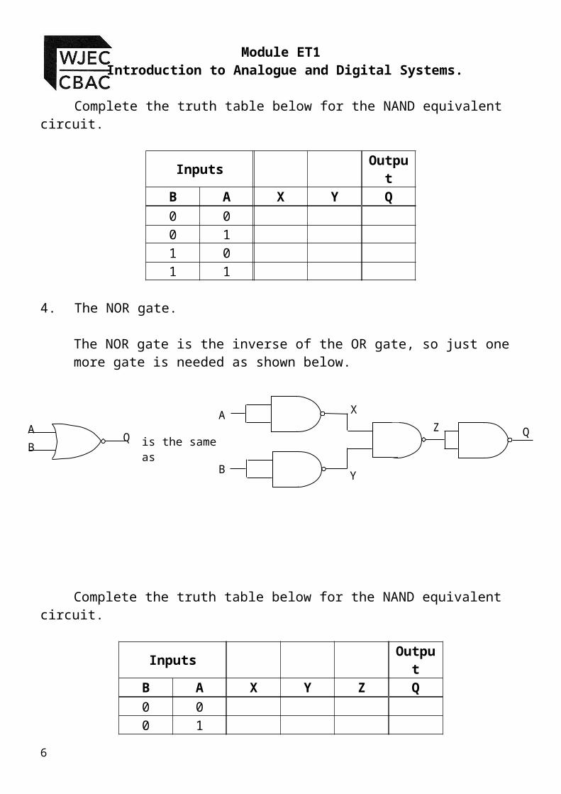
4. The NOR gate.
The NOR gate is the inverse of the OR gate, so just one more gate is needed as shown below.
Complete the truth table below for the NAND equivalent circuit.
Inputs Output
B A X Y Z Q0 00 11 01 1
5
is the same as
A
B
Q
MX
NY
OZA
BQ
P
Module ET1 Introduction to Analogue and Digital Systems.
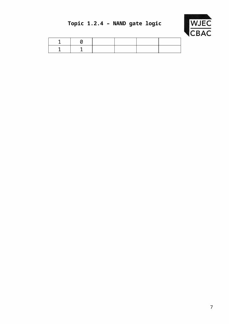
5. The ExOR gate.
The ExOR gate is quite a complex gate to construct using NAND gates the inverse of the OR gate, so just one more gate is needed as shown below.
Complete the truth table below for the NAND equivalent circuit.
Inputs Output
B A M N O P Q0 00 11 01 1
6
is the same as
A
B
QRX
SOZ
A
BQ
TP
is the same as
A
B
QAB
Q
Topic 1.2.4 – NAND gate logic
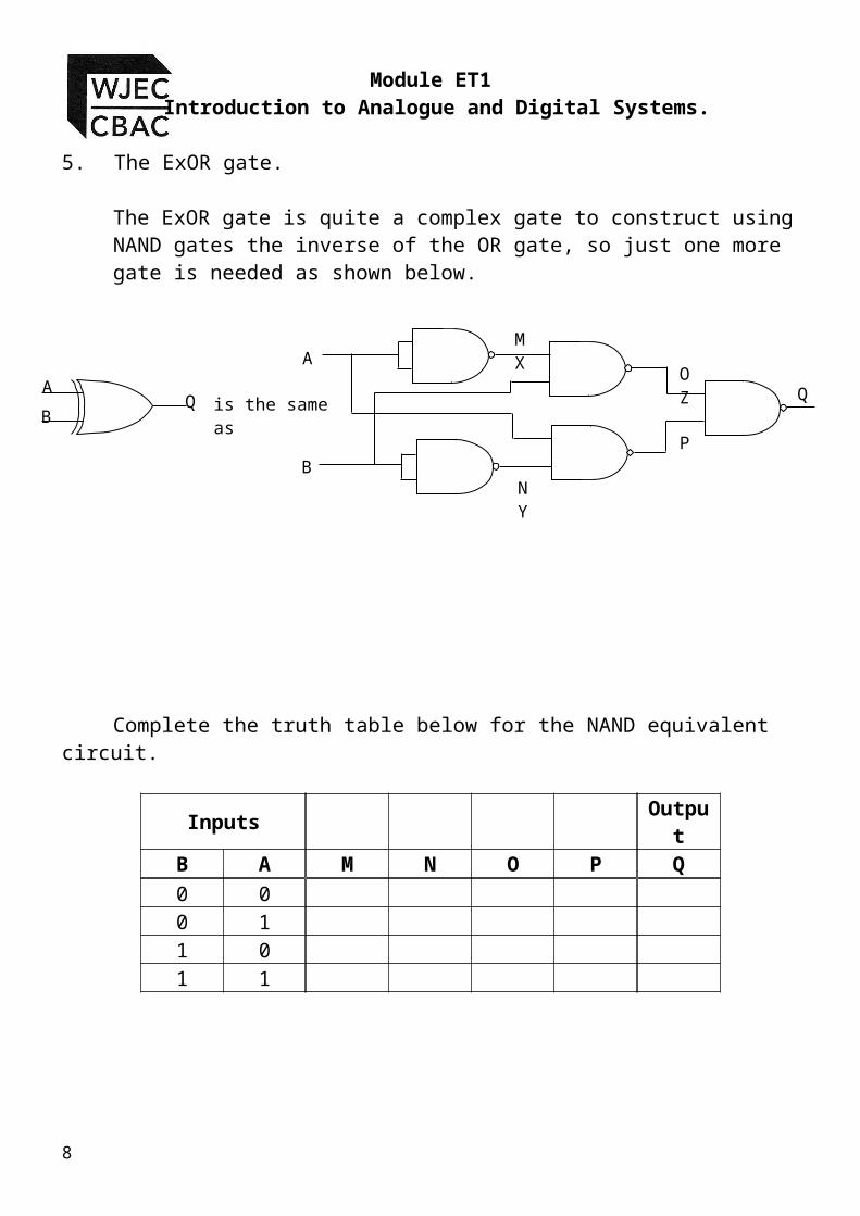
There is another version of the ExOr gate, which uses just four NAND gates, as shown below.
Complete the truth table below for the NAND equivalent circuit.
Inputs Output
B A R S T Q0 00 11 01 1
6. The ExNOR gate.
The ExNOR gate is simply the inverse of the ExOR gate. You should have done enough of these by now to be able to draw this yourself. Complete the diagram as before.
7
Module ET1 Introduction to Analogue and Digital Systems.
8
Topic 1.2.4 – NAND gate logic
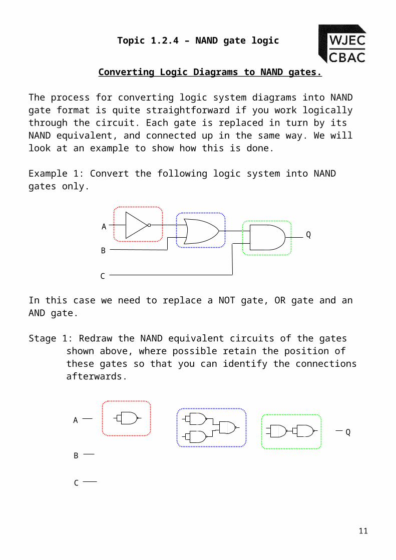
Converting Logic Diagrams to NAND gates.
The process for converting logic system diagrams into NAND gate format is quite straightforward if you work logically through the circuit. Each gate is replaced in turn by its NAND equivalent, and connected up in the same way. We will look at an example to show how this is done.
Example 1: Convert the following logic system into NAND gates only.
In this case we need to replace a NOT gate, OR gate and an AND gate.
Stage 1: Redraw the NAND equivalent circuits of the gates shown above, where possible retain the position of these gates so that you can identify the connections afterwards.
Drawing a box around each gate and it’s corresponding NAND equivalent will allow you to check that you have replaced every gate in the circuit.
9
AQ
B
C
QA
B
C
Module ET1 Introduction to Analogue and Digital Systems.
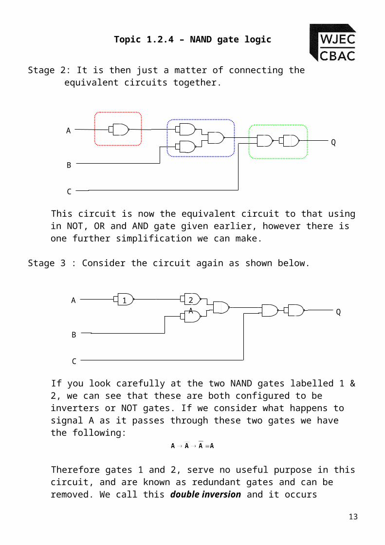
Stage 2: It is then just a matter of connecting the equivalent circuits together.
This circuit is now the equivalent circuit to that using in NOT, OR and AND gate given earlier, however there is one further simplification we can make.
Stage 3 : Consider the circuit again as shown below.
If you look carefully at the two NAND gates labelled 1 & 2, we can see that these are both configured to be inverters or NOT gates. If we consider what happens to signal A as it passes through these two gates we have the following:
Therefore gates 1 and 2, serve no useful purpose in this circuit, and are known as redundant gates and can be removed. We call this double inversion and it occurs commonly when creating NAND gate circuits from other logic systems.
10
AQ
B
C
AQ
B
C
1 2A
Topic 1.2.4 – NAND gate logic
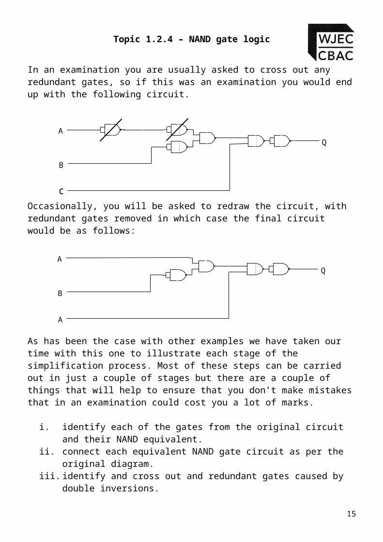
In an examination you are usually asked to cross out any redundant gates, so if this was an examination you would end up with the following circuit.
Occasionally, you will be asked to redraw the circuit, with redundant gates removed in which case the final circuit would be as follows:
As has been the case with other examples we have taken our time with this one to illustrate each stage of the simplification process. Most of these steps can be carried out in just a couple of stages but there are a couple of things that will help to ensure that you don’t make mistakes that in an examination could cost you a lot of marks.
i. identify each of the gates from the original circuit and their NAND equivalent.
ii. connect each equivalent NAND gate circuit as per the original diagram.
iii. identify and cross out and redundant gates caused by double inversions.
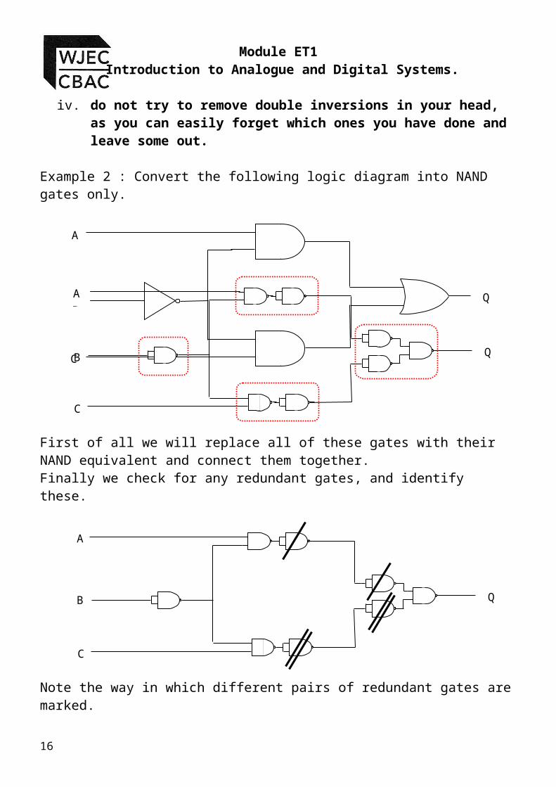
iv. do not try to remove double inversions in your head, as you can easily forget which ones you have done and leave some out.
Example 2 : Convert the following logic diagram into NAND gates only.
11
AQ
B
CC
AQ
B
A
Module ET1 Introduction to Analogue and Digital Systems.
First of all we will replace all of these gates with their NAND equivalent and connect them together.Finally we check for any redundant gates, and identify these.
Note the way in which different pairs of redundant gates are marked.
12
C
Q
A
B
C
Q
A
B
A
C
Q
A
B
AB
C
Q
Topic 1.2.4 – NAND gate logic
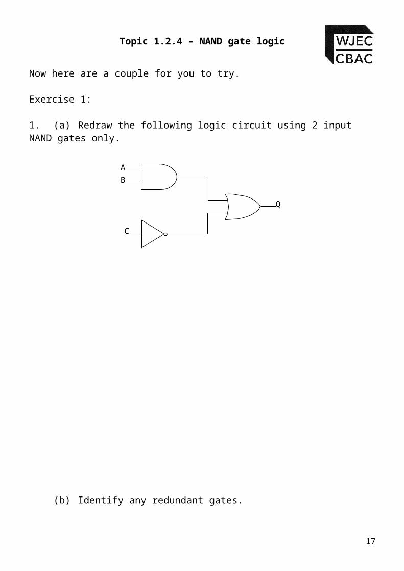
Now here are a couple for you to try.
Exercise 1:
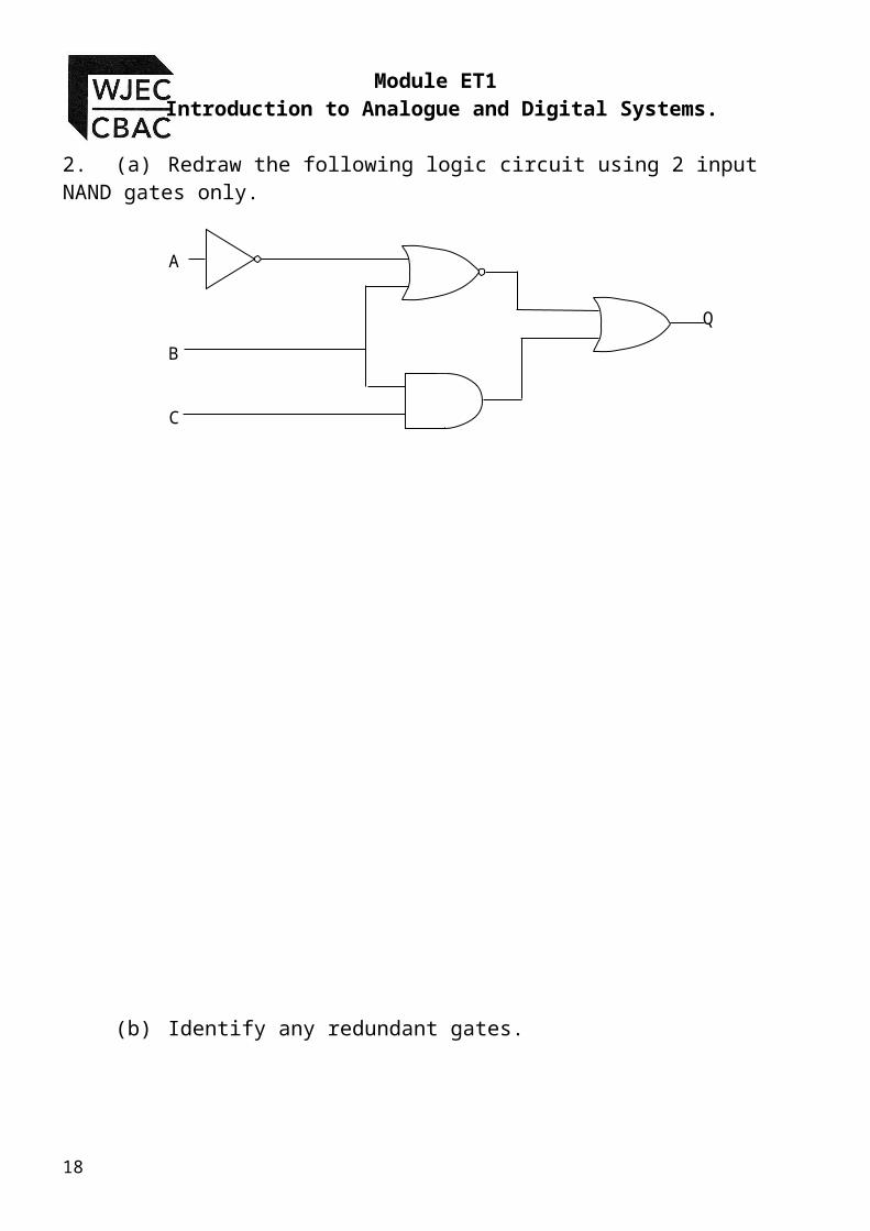
1. (a) Redraw the following logic circuit using 2 input NAND gates only.
(b) Identify any redundant gates.
13
A
Q
B
C
Module ET1 Introduction to Analogue and Digital Systems.
2. (a) Redraw the following logic circuit using 2 input NAND gates only.
(b) Identify any redundant gates.
14
Q
A
B
C
A
Q
B
C
* *
*
A
Topic 1.2.4 – NAND gate logic
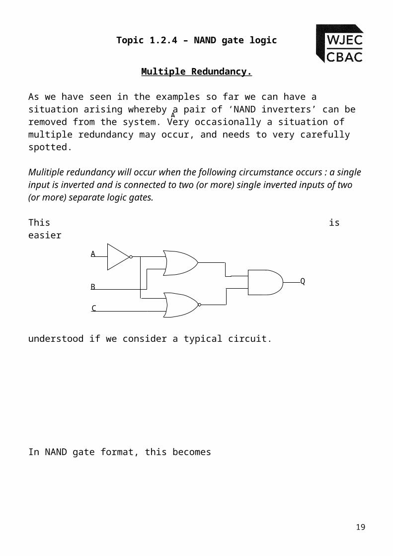
Multiple Redundancy.
As we have seen in the examples so far we can have a situation arising whereby a pair of ‘NAND inverters’ can be removed from the system. Very occasionally a situation of multiple redundancy may occur, and needs to very carefully spotted.
Mulitiple redundancy will occur when the following circumstance occurs : a single input is inverted and is connected to two (or more) single inverted inputs of two (or more) separate logic gates.
This is easier
understood if we consider a typical circuit.
In NAND gate format, this becomes
15
A
AA
AQ
AA
is the same as is the same asA
A
A
A
A A
A
Q
B
C
* *
*
Module ET1 Introduction to Analogue and Digital Systems.
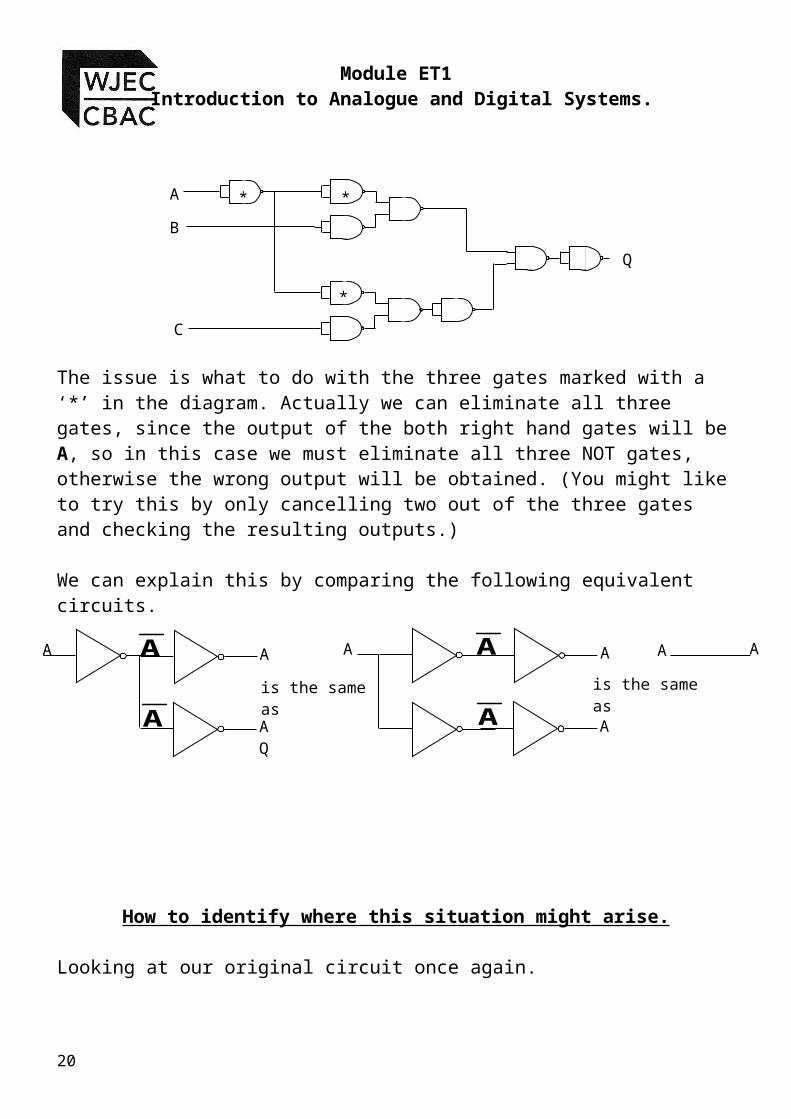
The issue is what to do with the three gates marked with a ‘*’ in the diagram. Actually we can eliminate all three gates, since the output of the both right hand gates will be A, so in this case we must eliminate all three NOT gates, otherwise the wrong output will be obtained. (You might like to try this by only cancelling two out of the three gates and checking the resulting outputs.)
We can explain this by comparing the following equivalent circuits.
How to identify where this situation might arise.
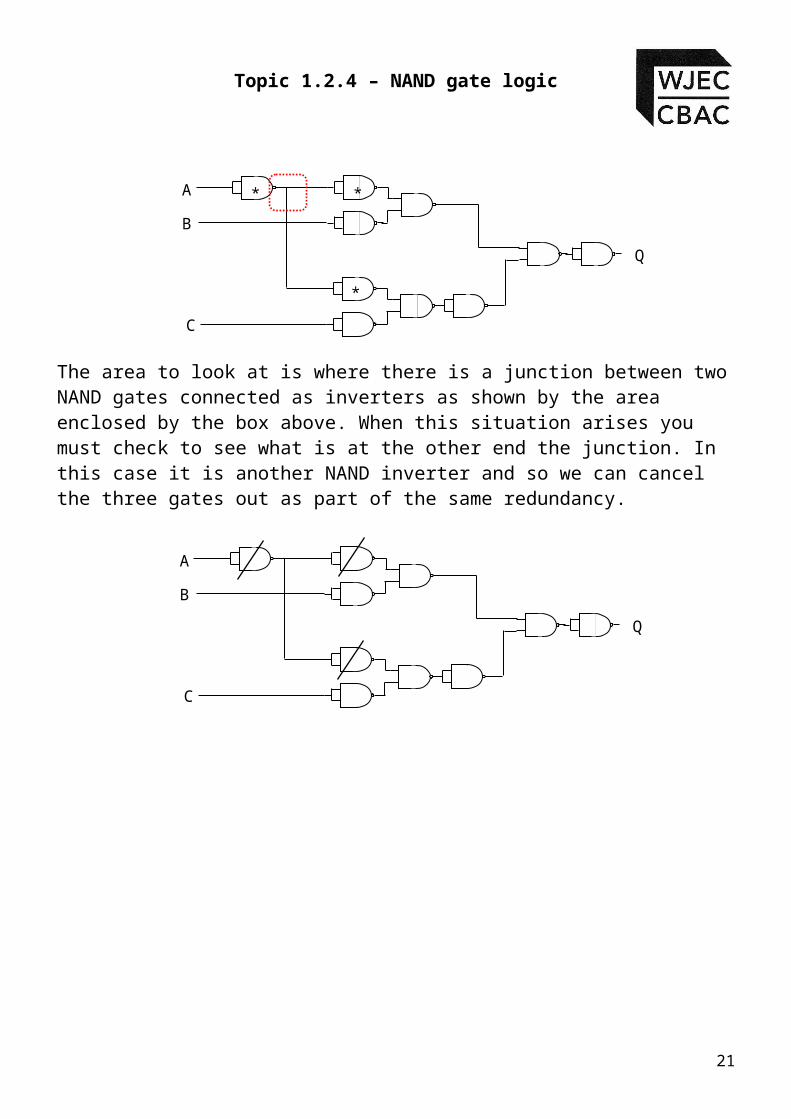
Looking at our original circuit once again.
The area to look at is where there is a junction between two NAND gates connected as inverters as shown by the area enclosed by the box above. When this situation arises you must check to see what is at the other end the junction. In this case it is another NAND inverter and so we can cancel the three gates out as part of the same redundancy.
16
A
Q
B
C
Topic 1.2.4 – NAND gate logic
17
Q
A
B
C
A
Q
B
C
* *
*
A
A
Q
B
C
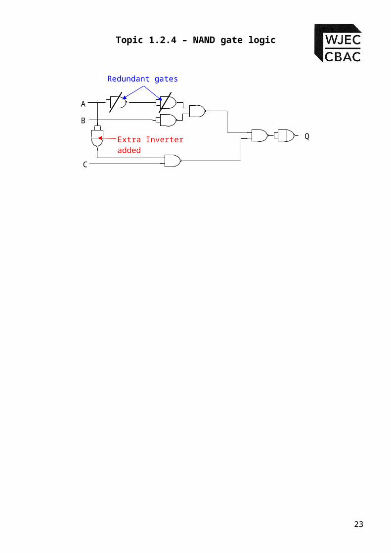
Extra Inverter added
Redundant gates cancelled
Module ET1 Introduction to Analogue and Digital Systems.
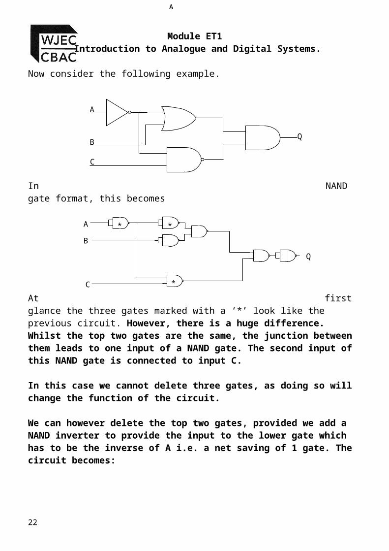
Now consider the following example.
In NAND gate format, this becomes
At first glance the three gates marked with a ‘*’ look like the previous circuit. However, there is a huge difference. Whilst the top two gates are the same, the junction between them leads to one input of a NAND gate. The second input of this NAND gate is connected to input C.
In this case we cannot delete three gates, as doing so will change the function of the circuit.
We can however delete the top two gates, provided we add a NAND inverter to provide the input to the lower gate which has to be the inverse of A i.e. a net saving of 1 gate. The circuit becomes:
18
Topic 1.2.4 – NAND gate logic
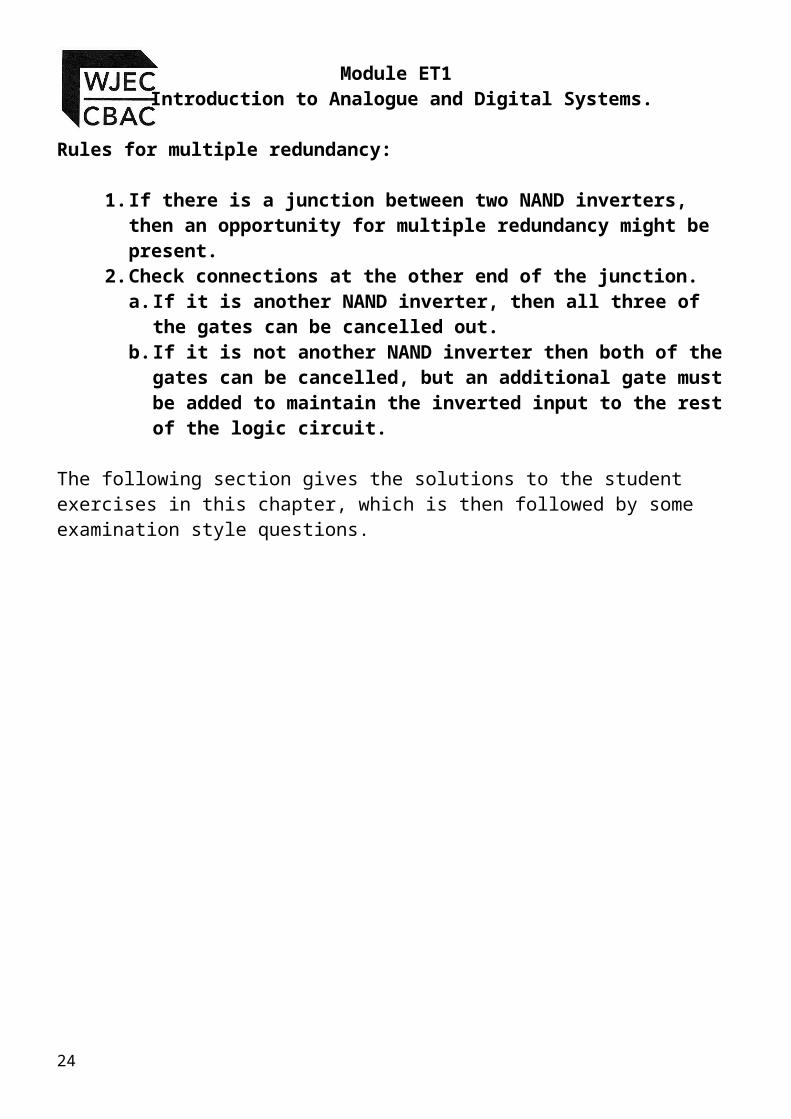
Rules for multiple redundancy:
1. If there is a junction between two NAND inverters, then an opportunity for multiple redundancy might be present.
2. Check connections at the other end of the junction.a. If it is another NAND inverter, then all three of the
gates can be cancelled out.b. If it is not another NAND inverter then both of the
gates can be cancelled, but an additional gate must be added to maintain the inverted input to the rest of the logic circuit.
The following section gives the solutions to the student exercises in this chapter, which is then followed by some examination style questions.
19
A
QB
C
A
QB
C
A
Q
B
Module ET1 Introduction to Analogue and Digital Systems.
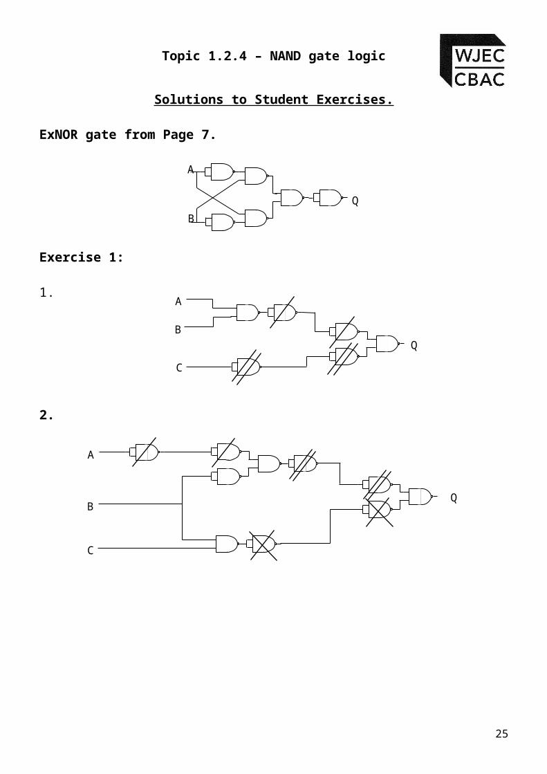
Solutions to Student Exercises.
ExNOR gate from Page 7.
Exercise 1:
1.
2.
20
Topic 1.2.4 – NAND gate logic
Examination Style Questions.
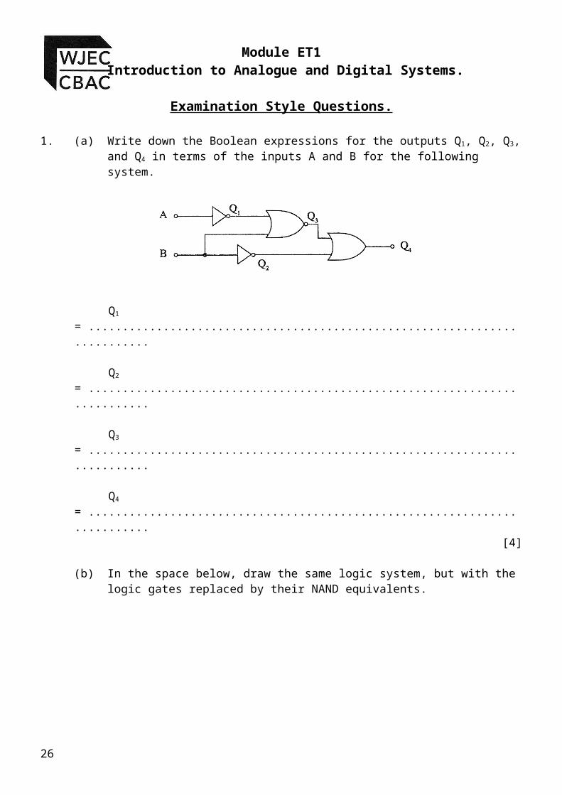
1. (a) Write down the Boolean expressions for the outputs Q1, Q2, Q3, and Q4 in terms of the inputs A and B for the following system.
Q1 = ..........................................................................
Q2 = ..........................................................................
Q3 = ..........................................................................
Q4 = ..........................................................................[4]
(b) In the space below, draw the same logic system, but with the logic gates replaced by their NAND equivalents.
[3]
(c) Draw a line through all redundant NAND gates.[2]
21
Module ET1 Introduction to Analogue and Digital Systems.
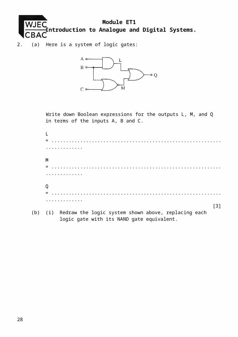
2. (a) Here is a system of logic gates:
Write down Boolean expressions for the outputs L, M, and Q in terms of the inputs A, B and C.
L = ........................................................................
M = ........................................................................
Q = ........................................................................[3]
(b) (i) Redraw the logic system shown above, replacing each logic gate with its NAND gate equivalent.
[3](ii) Identify any redundant gates in the system you have just drawn.
[2](iii) How many redundant gates are there ? ................................
[1]
22
Topic 1.2.4 – NAND gate logic
3. Here is a system of logic gates.
Write down Boolean expressions for the outputs X, Y, and Q in terms of the inputs A and B.
X = ........................................................................
Y = ........................................................................
Q = ........................................................................[3]
(b) (i) Redraw the logic system shown above, replacing each logic gate with its NAND gate equivalent.
[3](ii) Identify any redundant gates in the system you have just drawn.
[1](iii) Explain why it can be cheaper to convert logic systems to their NAND gate
equivalents.
..................................................................................................................................................
..................................................................................................................................................
..................................................................................................................................................[1]
23
Module ET1 Introduction to Analogue and Digital Systems.
4. The following diagram shows a logic circuit.
(a) Redraw the logic system shown above, replacing each logic gate with its NAND gate equivalent.
[3](b) Identify any redundant gates in the system you have just drawn.
[1]
24
Topic 1.2.4 – NAND gate logic
25
Module ET1 Introduction to Analogue and Digital Systems.
5. (a) Show how a logic system can be made up, using AND, OR and NOT gates, for the expression:
[3]
(b) Redraw the system using 2-input NAND gates only.
[3]
(c) Cross out all redundant gates in the diagram above.[2]
26
Topic 1.2.4 – NAND gate logic
6. A logic system is shown below.
(a) Complete the truth table for this system.
A B C D Q0 00 11 01 1
[3]
(b) In the space below, draw the same logic system, but with the logic gates replaced by their NAND gate equivalents.
[3]
(c) Draw lines through all redundant gates.[2]
7. The diagram below shows a logic system.
27
Module ET1 Introduction to Analogue and Digital Systems.
(a) (i) In the space below, draw the same logic system, but with the logic gates replaced by their NAND gate equivalents.
[3]
(ii) How many pairs of redundant gates are there in this system ? ............................[1]
(b) Redraw the simplified system in the space below.
[1]
28
Topic 1.2.4 – NAND gate logic
Self Evaluation Review
Learning ObjectivesMy personal review of these objectives:
Use combinations of NAND gates to perform other logic functions;Implement a logic system using only NAND gates;Recognise redundant gates in a logic system constructed only from NAND gates.
Targets: 1.
………………………………………………………………………………………………………………
………………………………………………………………………………………………………………
2. ………………………………………………………………………………………………………………
………………………………………………………………………………………………………………
29


![Gates and Logic: From Transistors to Logic Gates and Logic ......Gates and Logic: From Transistors to Logic Gates and Logic Circuits [Weatherspoon, Bala, Bracy, and Sirer] Prof. Hakim](https://img.pdfslide.us/doc/110x75/5fa95cb6eb1af8231472f381/gates-and-logic-from-transistors-to-logic-gates-and-logic-gates-and-logic.jpg)