Embed Size (px)
Citation preview
Stratix IV Device Handbook Volume 1February 2011
SIV51002-3.1
© 2011 Altera Corporation. All rights reserved. ALTERA, ARRand/or trademarks of Altera Corporation in the U.S. and otherwww.altera.com/common/legal.html. Altera warrants performreserves the right to make changes to any products and servicesinformation, product, or service described herein except as expspecifications before relying on any published information and
February 2011SIV51002-3.1
2. Logic Array Blocks and Adaptive LogicModules in Stratix IV Devices
This chapter describes the features of the logic array blocks (LABs) in the Stratix® IV core fabric. LABs are made up of adaptive logic modules (ALMs) that you can configure to implement logic functions, arithmetic functions, and register functions.
LABs and ALMs are the basic building blocks of the Stratix IV device. Use these to configure logic, arithmetic, and register functions. The ALM provides advanced features with efficient logic usage and is completely backward-compatible.
This chapter contains the following sections:
■ “Logic Array Blocks”
■ “Adaptive Logic Modules” on page 2–5
Logic Array BlocksEach LAB consists of ten ALMs, various carry chains, shared arithmetic chains, LAB control signals, local interconnect, and register chain connection lines. The local interconnect transfers signals between ALMs in the same LAB. The direct link interconnect allows the LAB to drive into the local interconnect of its left and right neighbors. Register chain connections transfer the output of the ALM register to the adjacent ALM register in the LAB. The Quartus® II Compiler places associated logic in the LAB or adjacent LABs, allowing the use of local, shared arithmetic chain, and register chain connections for performance and area efficiency.
Subscribe
IA, CYCLONE, HARDCOPY, MAX, MEGACORE, NIOS, QUARTUS and STRATIX are Reg. U.S. Pat. & Tm. Off. countries. All other trademarks and service marks are the property of their respective holders as described at
ance of its semiconductor products to current specifications in accordance with Altera’s standard warranty, but at any time without notice. Altera assumes no responsibility or liability arising out of the application or use of any ressly agreed to in writing by Altera. Altera customers are advised to obtain the latest version of device before placing orders for products or services.
2–2 Chapter 2: Logic Array Blocks and Adaptive Logic Modules in Stratix IV DevicesLogic Array Blocks
Figure 2–1 shows the Stratix IV LAB structure and interconnects.
The LAB of the Stratix IV device has a derivative called memory LAB (MLAB), which adds look-up table (LUT)-based SRAM capability to the LAB, as shown in Figure 2–2. The MLAB supports a maximum of 640 bits of simple dual-port static random access memory (SRAM). You can configure each ALM in an MLAB as either a 64 × 1 or a 32 × 2 block, resulting in a configuration of either a 64 × 10 or a 32 × 20 simple dual-port SRAM block. MLAB and LAB blocks always coexist as pairs in all Stratix IV families. MLAB is a superset of the LAB and includes all LAB features.
Figure 2–1. Stratix IV LAB Structure and Interconnects
Direct linkinterconnect fromadjacent block
Direct linkinterconnect toadjacent block
Row Interconnects ofVariable Speed & Length
Column Interconnects ofVariable Speed & LengthLocal Interconnect is Driven
from Either Side by Columns & LABs, & from Above by Rows
Local Interconnect LAB
Direct linkinterconnect from adjacent block
Direct linkinterconnect toadjacent block
ALMs
MLAB
C4 C12
R20
R4
Stratix IV Device Handbook Volume 1 February 2011 Altera Corporation
Chapter 2: Logic Array Blocks and Adaptive Logic Modules in Stratix IV Devices 2–3Logic Array Blocks
f The MLAB is described in detail in the TriMatrix Embedded Memory Blocks in Stratix IV Devices chapter.
Figure 2–2. Stratix IV LAB and MLAB Structure
Note to Figure 2–2:(1) You can use the MLAB ALM as a regular LAB ALM or configure it as a dual-port SRAM, as shown.
MLAB LAB
LUT-based-64 x 1Simple dual-port SRAM
LUT-based-64 x 1Simple dual-port SRAM
LUT-based-64 x 1Simple dual-port SRAM
LUT-based-64 x 1Simple dual-port SRAM
LUT-based-64 x 1Simple dual-port SRAM
LUT-based-64 x 1Simple dual-port SRAM
LUT-based-64 x 1Simple dual-port SRAM
LUT-based-64 x 1Simple dual-port SRAM
LUT-based-64 x 1Simple dual-port SRAM
LUT-based-64 x 1Simple dual-port SRAM
(1)
(1)
(1)
(1)
(1)
(1)
(1)
(1)
(1)
(1)
ALM
ALM
ALM
ALM
ALM
ALM
ALM
ALM
ALM
ALM
LAB Control BlockLAB Control Block
February 2011 Altera Corporation Stratix IV Device Handbook Volume 1
2–4 Chapter 2: Logic Array Blocks and Adaptive Logic Modules in Stratix IV DevicesLogic Array Blocks
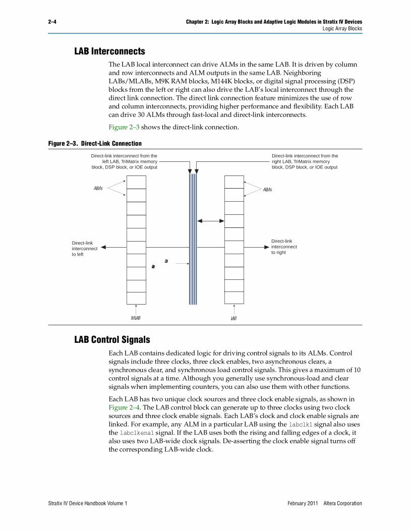
LAB InterconnectsThe LAB local interconnect can drive ALMs in the same LAB. It is driven by column and row interconnects and ALM outputs in the same LAB. Neighboring LABs/MLABs, M9K RAM blocks, M144K blocks, or digital signal processing (DSP) blocks from the left or right can also drive the LAB’s local interconnect through the direct link connection. The direct link connection feature minimizes the use of row and column interconnects, providing higher performance and flexibility. Each LAB can drive 30 ALMs through fast-local and direct-link interconnects.
Figure 2–3 shows the direct-link connection.
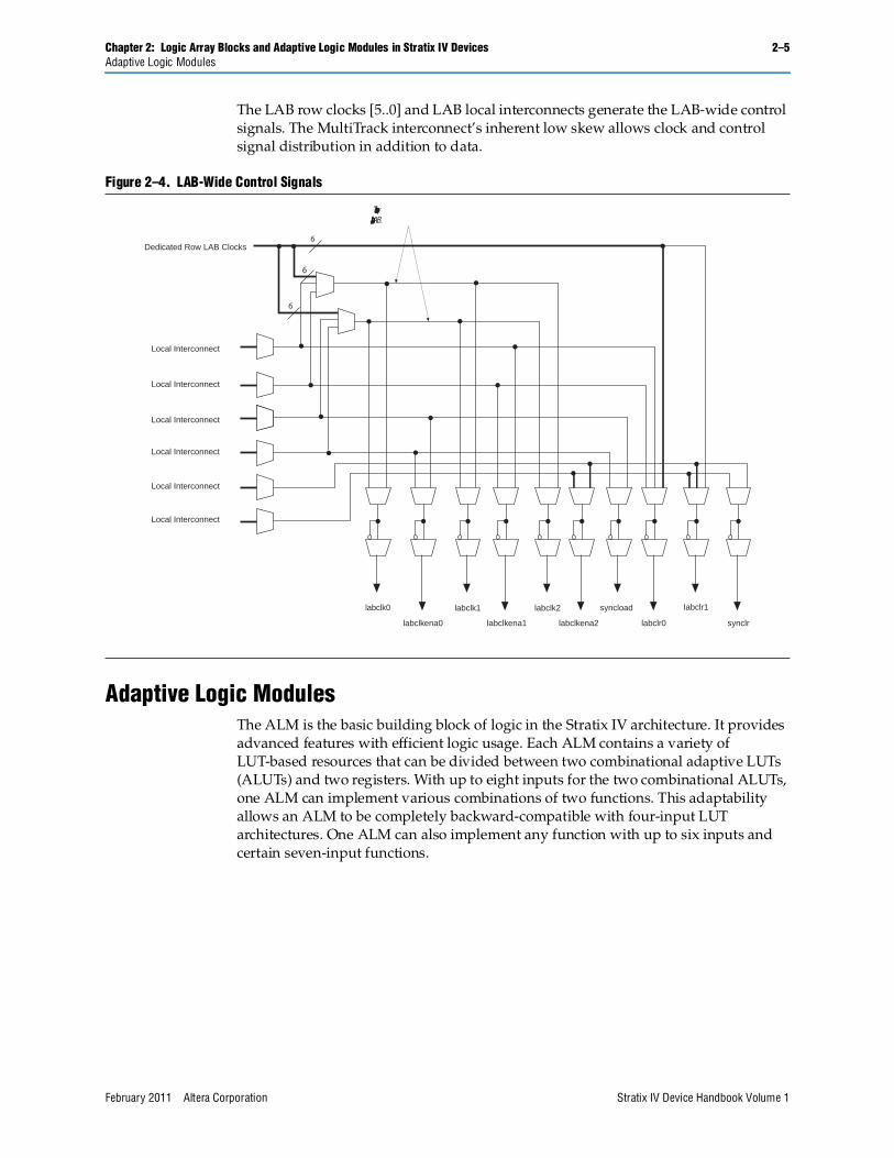
LAB Control SignalsEach LAB contains dedicated logic for driving control signals to its ALMs. Control signals include three clocks, three clock enables, two asynchronous clears, a synchronous clear, and synchronous load control signals. This gives a maximum of 10 control signals at a time. Although you generally use synchronous-load and clear signals when implementing counters, you can also use them with other functions.
Each LAB has two unique clock sources and three clock enable signals, as shown in Figure 2–4. The LAB control block can generate up to three clocks using two clock sources and three clock enable signals. Each LAB’s clock and clock enable signals are linked. For example, any ALM in a particular LAB using the labclk1 signal also uses the labclkena1 signal. If the LAB uses both the rising and falling edges of a clock, it also uses two LAB-wide clock signals. De-asserting the clock enable signal turns off the corresponding LAB-wide clock.
Figure 2–3. Direct-Link Connection
ALMs
Direct-linkinterconnectto right
Direct-link interconnect from the right LAB, TriMatrix memoryblock, DSP block, or IOE output
Direct-link interconnect from theleft LAB, TriMatrix memory
block, DSP block, or IOE output
LocalInterconnect
LAB
ALMs
Direct-linkinterconnectto left
MLAB
Stratix IV Device Handbook Volume 1 February 2011 Altera Corporation
Chapter 2: Logic Array Blocks and Adaptive Logic Modules in Stratix IV Devices 2–5Adaptive Logic Modules
The LAB row clocks [5..0] and LAB local interconnects generate the LAB-wide control signals. The MultiTrack interconnect’s inherent low skew allows clock and control signal distribution in addition to data.
Adaptive Logic ModulesThe ALM is the basic building block of logic in the Stratix IV architecture. It provides advanced features with efficient logic usage. Each ALM contains a variety of LUT-based resources that can be divided between two combinational adaptive LUTs (ALUTs) and two registers. With up to eight inputs for the two combinational ALUTs, one ALM can implement various combinations of two functions. This adaptability allows an ALM to be completely backward-compatible with four-input LUT architectures. One ALM can also implement any function with up to six inputs and certain seven-input functions.
Figure 2–4. LAB-Wide Control Signals
Dedicated Row LAB Clocks
Local Interconnect
Local Interconnect
Local Interconnect
Local Interconnect
Local Interconnect
Local Interconnect
labclk2 syncload
labclkena0or asyncloador labpreset
labclk0 labclk1 labclr1
labclkena1 labclkena2 labclr0 synclr
6
6
6
There are two uniqueclock signals per LAB.
February 2011 Altera Corporation Stratix IV Device Handbook Volume 1
2–6 Chapter 2: Logic Array Blocks and Adaptive Logic Modules in Stratix IV DevicesAdaptive Logic Modules
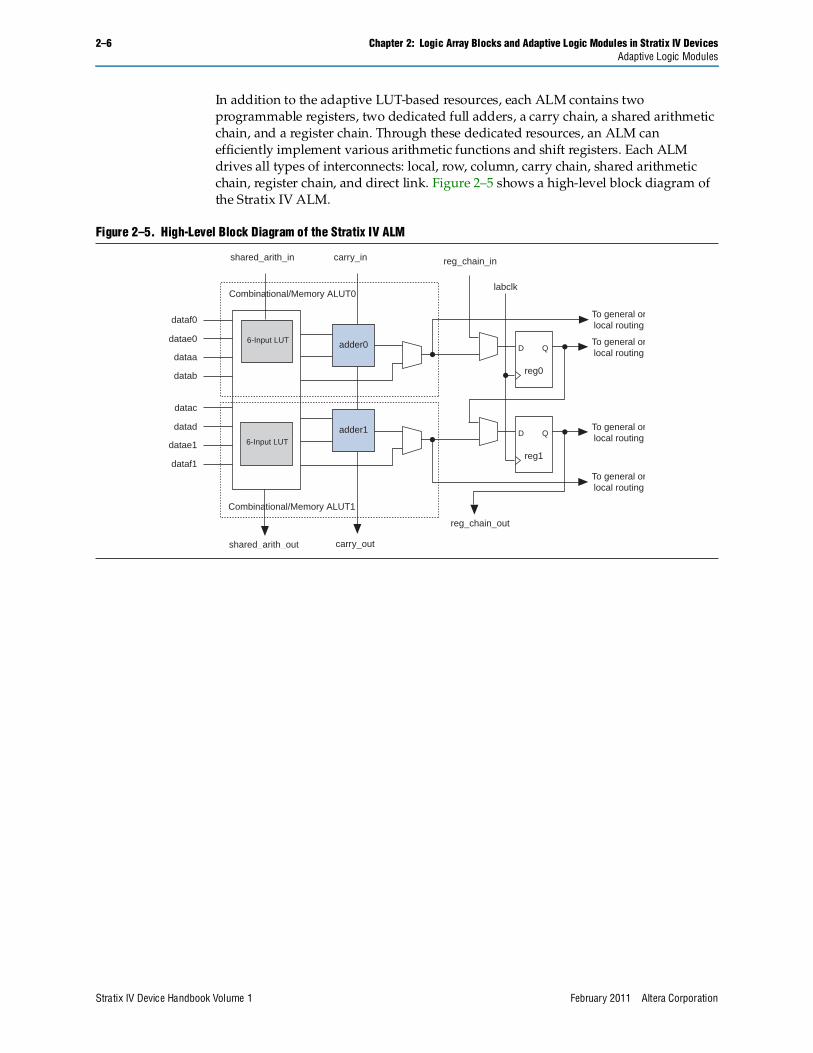
In addition to the adaptive LUT-based resources, each ALM contains two programmable registers, two dedicated full adders, a carry chain, a shared arithmetic chain, and a register chain. Through these dedicated resources, an ALM can efficiently implement various arithmetic functions and shift registers. Each ALM drives all types of interconnects: local, row, column, carry chain, shared arithmetic chain, register chain, and direct link. Figure 2–5 shows a high-level block diagram of the Stratix IV ALM.
Figure 2–5. High-Level Block Diagram of the Stratix IV ALM
D QTo general orlocal routing
reg0
To general orlocal routing
datae0
dataf0
reg_chain_in
reg_chain_out
adder0dataa
datab
datac
datad
datae1
dataf1
D QTo general orlocal routing
reg1
To general orlocal routing
adder1
carry_in
carry_out
Combinational/Memory ALUT0
6-Input LUT
6-Input LUT
shared_arith_out
shared_arith_in
Combinational/Memory ALUT1
labclk
Stratix IV Device Handbook Volume 1 February 2011 Altera Corporation
Chapter 2: Logic Array Blocks and Adaptive Logic Modules in Stratix IV Devices 2–7Adaptive Logic Modules
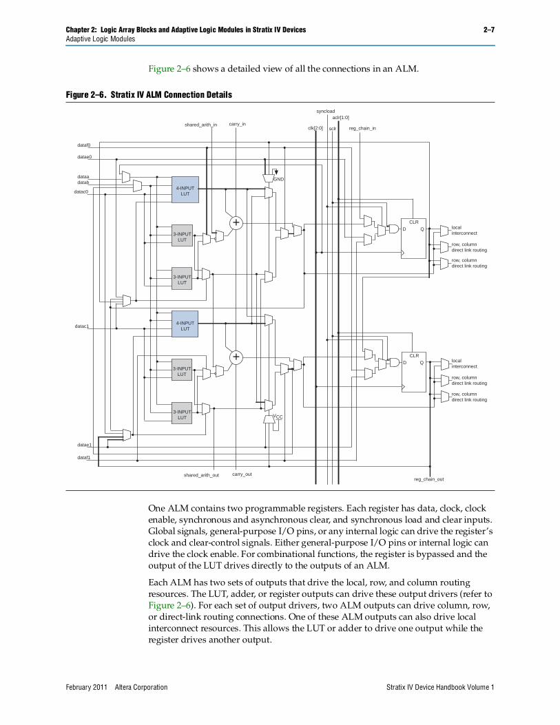
Figure 2–6 shows a detailed view of all the connections in an ALM.
One ALM contains two programmable registers. Each register has data, clock, clock enable, synchronous and asynchronous clear, and synchronous load and clear inputs. Global signals, general-purpose I/O pins, or any internal logic can drive the register’s clock and clear-control signals. Either general-purpose I/O pins or internal logic can drive the clock enable. For combinational functions, the register is bypassed and the output of the LUT drives directly to the outputs of an ALM.
Each ALM has two sets of outputs that drive the local, row, and column routing resources. The LUT, adder, or register outputs can drive these output drivers (refer to Figure 2–6). For each set of output drivers, two ALM outputs can drive column, row, or direct-link routing connections. One of these ALM outputs can also drive local interconnect resources. This allows the LUT or adder to drive one output while the register drives another output.
Figure 2–6. Stratix IV ALM Connection Details
D Q+
reg_chain_in
aclr[1:0]
sclr
syncload
clk[2:0]carry_in
dataf0
datae0
dataadatab
datac1
datae1
dataf1
shared_arith_out carry_outreg_chain_out
CLR
D Q
CLR
shared_arith_in
local interconnect
row, columndirect link routing
row, columndirect link routing
local interconnect
4-INPUTLUT
4-INPUTLUT
3-INPUTLUT
3-INPUTLUT
3-INPUTLUT
3-INPUTLUT
+
datac0
VCC
GND
row, columndirect link routing
row, columndirect link routing
February 2011 Altera Corporation Stratix IV Device Handbook Volume 1
2–8 Chapter 2: Logic Array Blocks and Adaptive Logic Modules in Stratix IV DevicesAdaptive Logic Modules
This feature, called register packing, improves device utilization because the device can use the register and the combinational logic for unrelated functions. Another special packing mode allows the register output to feed back into the LUT of the same ALM so that the register is packed with its own fan-out LUT. This provides another mechanism for improved fitting. The ALM can also drive out registered and unregistered versions of the LUT or adder output.
ALM Operating ModesThe Stratix IV ALM operates in one of the following modes:
■ Normal
■ Extended LUT
■ Arithmetic
■ Shared Arithmetic
■ LUT-Register
Each mode uses ALM resources differently. In each mode, eleven available inputs to an ALM—the eight data inputs from the LAB local interconnect, carry-in from the previous ALM or LAB, the shared arithmetic chain connection from the previous ALM or LAB, and the register chain connection—are directed to different destinations to implement the desired logic function. LAB-wide signals provide clock, asynchronous clear, synchronous clear, synchronous load, and clock enable control for the register. These LAB-wide signals are available in all ALM modes.
For more information about the LAB-wide control signals, refer to “LAB Control Signals” on page 2–4.
The Quartus II software and supported third-party synthesis tools, in conjunction with parameterized functions such as the library of parameterized modules (LPM) functions, automatically choose the appropriate mode for common functions such as counters, adders, subtractors, and arithmetic functions.
Stratix IV Device Handbook Volume 1 February 2011 Altera Corporation
Chapter 2: Logic Array Blocks and Adaptive Logic Modules in Stratix IV Devices 2–9Adaptive Logic Modules
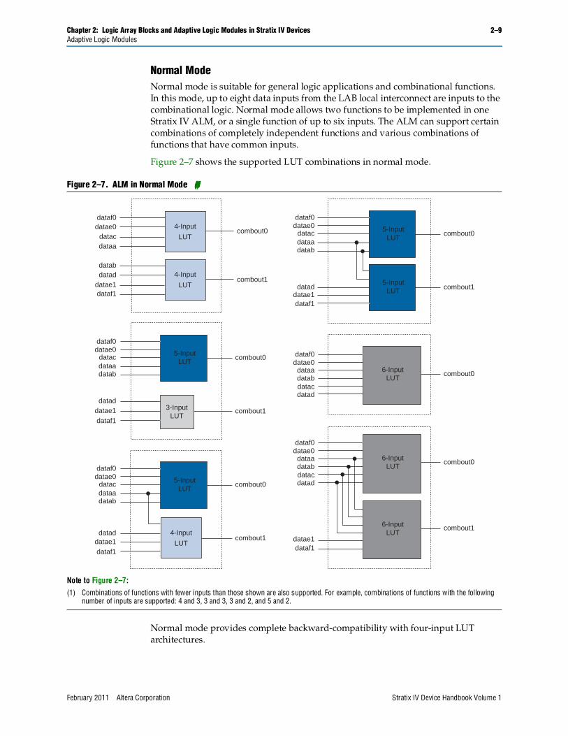
Normal ModeNormal mode is suitable for general logic applications and combinational functions. In this mode, up to eight data inputs from the LAB local interconnect are inputs to the combinational logic. Normal mode allows two functions to be implemented in one Stratix IV ALM, or a single function of up to six inputs. The ALM can support certain combinations of completely independent functions and various combinations of functions that have common inputs.
Figure 2–7 shows the supported LUT combinations in normal mode.
Normal mode provides complete backward-compatibility with four-input LUT architectures.
Figure 2–7. ALM in Normal Mode (Note 1)
Note to Figure 2–7:(1) Combinations of functions with fewer inputs than those shown are also supported. For example, combinations of functions with the following
number of inputs are supported: 4 and 3, 3 and 3, 3 and 2, and 5 and 2.
6-InputLUT
dataf0datae0
dataf0datae0
dataadatab
dataadatab
datab
datac
datac
dataf0datae0
dataadatac
6-InputLUT
datad
datad
datae1
combout0
combout1
combout0
combout1
combout0
combout1
dataf1
datae1dataf1
dataddatae1dataf1
4-Input
LUT
4-Input
LUT
4-Input
LUT
6-InputLUT
dataf0datae0
dataadatabdatacdatad
combout0
5-InputLUT
5-InputLUT
dataf0datae0
dataadatab
datac
datad
combout0
combout1datae1dataf1
5-InputLUT
dataf0datae0
dataadatab
datac
datad
combout0
combout1datae1dataf1
5-InputLUT
3-InputLUT
February 2011 Altera Corporation Stratix IV Device Handbook Volume 1
2–10 Chapter 2: Logic Array Blocks and Adaptive Logic Modules in Stratix IV DevicesAdaptive Logic Modules
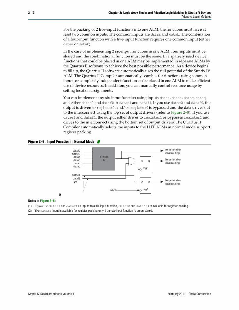
For the packing of 2 five-input functions into one ALM, the functions must have at least two common inputs. The common inputs are dataa and datab. The combination of a four-input function with a five-input function requires one common input (either dataa or datab).
In the case of implementing 2 six-input functions in one ALM, four inputs must be shared and the combinational function must be the same. In a sparsely used device, functions that could be placed in one ALM may be implemented in separate ALMs by the Quartus II software to achieve the best possible performance. As a device begins to fill up, the Quartus II software automatically uses the full potential of the Stratix IV ALM. The Quartus II Compiler automatically searches for functions using common inputs or completely independent functions to be placed in one ALM to make efficient use of device resources. In addition, you can manually control resource usage by setting location assignments.
You can implement any six-input function using inputs dataa, datab, datac, datad, and either datae0 and dataf0 or datae1 and dataf1. If you use datae0 and dataf0, the output is driven to register0, and/or register0 is bypassed and the data drives out to the interconnect using the top set of output drivers (refer to Figure 2–8). If you use datae1 and dataf1, the output either drives to register1 or bypasses register1 and drives to the interconnect using the bottom set of output drivers. The Quartus II Compiler automatically selects the inputs to the LUT. ALMs in normal mode support register packing.
Figure 2–8. Input Function in Normal Mode (Note 1)
Notes to Figure 2–8:(1) If you use datae1 and dataf1 as inputs to a six-input function, datae0 and dataf0 are available for register packing.(2) The dataf1 input is available for register packing only if the six-input function is unregistered.
6-InputLUT
dataf0datae0dataadatabdatacdatad
datae1dataf1
D Q
D Q
To general orlocal routing
To general orlocal routing
To general orlocal routing
reg0
reg1
These inputs are available for register packing.
(2)
labclk
Stratix IV Device Handbook Volume 1 February 2011 Altera Corporation
Chapter 2: Logic Array Blocks and Adaptive Logic Modules in Stratix IV Devices 2–11Adaptive Logic Modules
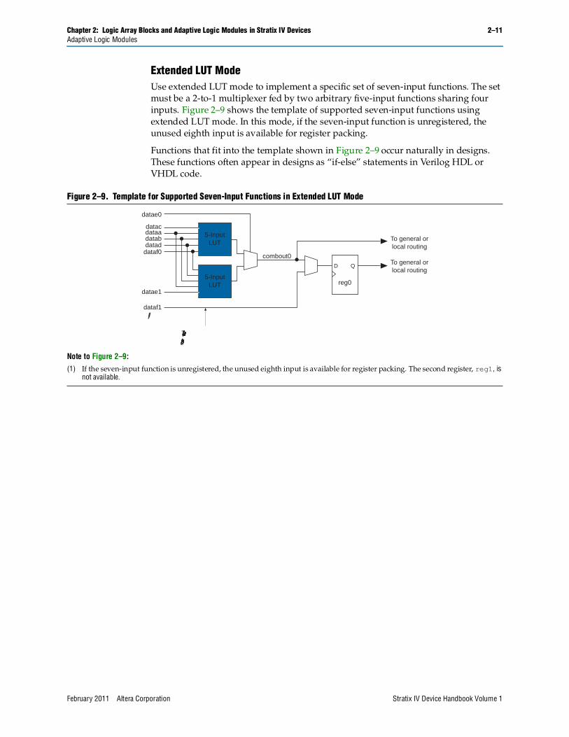
Extended LUT ModeUse extended LUT mode to implement a specific set of seven-input functions. The set must be a 2-to-1 multiplexer fed by two arbitrary five-input functions sharing four inputs. Figure 2–9 shows the template of supported seven-input functions using extended LUT mode. In this mode, if the seven-input function is unregistered, the unused eighth input is available for register packing.
Functions that fit into the template shown in Figure 2–9 occur naturally in designs. These functions often appear in designs as “if-else” statements in Verilog HDL or VHDL code.
Figure 2–9. Template for Supported Seven-Input Functions in Extended LUT Mode
Note to Figure 2–9:(1) If the seven-input function is unregistered, the unused eighth input is available for register packing. The second register, reg1, is
not available.
datae0
combout0
5-InputLUT
5-InputLUT
datacdataadatabdataddataf0
datae1
dataf1
D QTo general orlocal routing
To general orlocal routing
reg0
This input is availablefor register packing.
(1)
February 2011 Altera Corporation Stratix IV Device Handbook Volume 1
2–12 Chapter 2: Logic Array Blocks and Adaptive Logic Modules in Stratix IV DevicesAdaptive Logic Modules
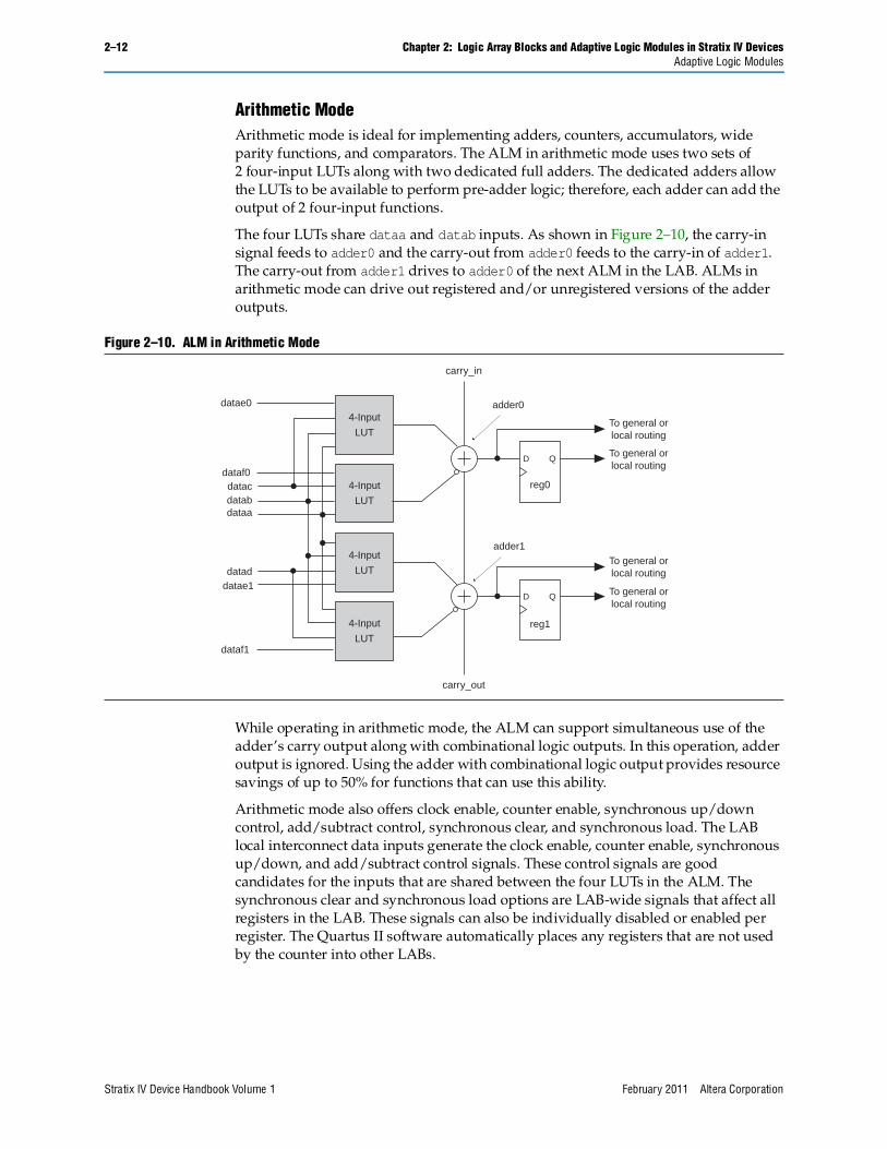
Arithmetic ModeArithmetic mode is ideal for implementing adders, counters, accumulators, wide parity functions, and comparators. The ALM in arithmetic mode uses two sets of 2 four-input LUTs along with two dedicated full adders. The dedicated adders allow the LUTs to be available to perform pre-adder logic; therefore, each adder can add the output of 2 four-input functions.
The four LUTs share dataa and datab inputs. As shown in Figure 2–10, the carry-in signal feeds to adder0 and the carry-out from adder0 feeds to the carry-in of adder1. The carry-out from adder1 drives to adder0 of the next ALM in the LAB. ALMs in arithmetic mode can drive out registered and/or unregistered versions of the adder outputs.
While operating in arithmetic mode, the ALM can support simultaneous use of the adder’s carry output along with combinational logic outputs. In this operation, adder output is ignored. Using the adder with combinational logic output provides resource savings of up to 50% for functions that can use this ability.
Arithmetic mode also offers clock enable, counter enable, synchronous up/down control, add/subtract control, synchronous clear, and synchronous load. The LAB local interconnect data inputs generate the clock enable, counter enable, synchronous up/down, and add/subtract control signals. These control signals are good candidates for the inputs that are shared between the four LUTs in the ALM. The synchronous clear and synchronous load options are LAB-wide signals that affect all registers in the LAB. These signals can also be individually disabled or enabled per register. The Quartus II software automatically places any registers that are not used by the counter into other LABs.
Figure 2–10. ALM in Arithmetic Mode
datae0
carry_in
carry_out
dataadatabdatac
dataddatae1
D Q
D Q
To general orlocal routing
To general orlocal routing
reg0
reg1
To general orlocal routing
To general orlocal routing
4-Input
LUT
4-Input
LUT
4-Input
LUT
4-Input
LUT
adder1
adder0
dataf0
dataf1
Stratix IV Device Handbook Volume 1 February 2011 Altera Corporation
Chapter 2: Logic Array Blocks and Adaptive Logic Modules in Stratix IV Devices 2–13Adaptive Logic Modules
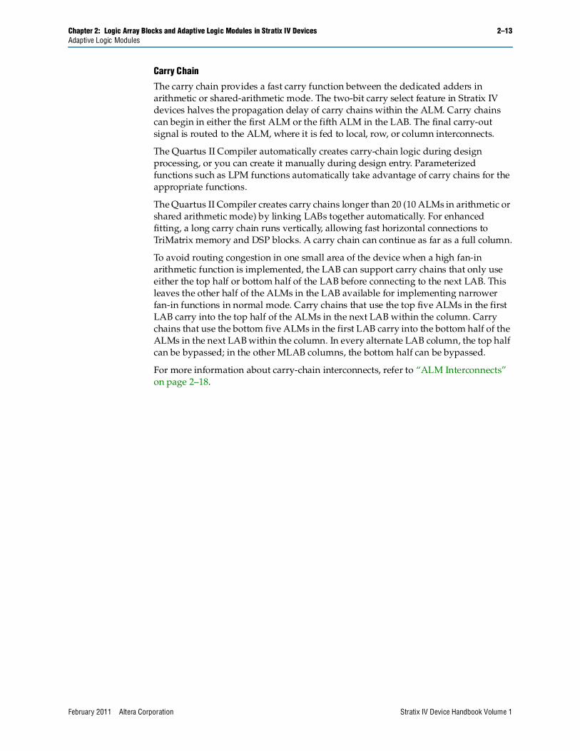
Carry Chain
The carry chain provides a fast carry function between the dedicated adders in arithmetic or shared-arithmetic mode. The two-bit carry select feature in Stratix IV devices halves the propagation delay of carry chains within the ALM. Carry chains can begin in either the first ALM or the fifth ALM in the LAB. The final carry-out signal is routed to the ALM, where it is fed to local, row, or column interconnects.
The Quartus II Compiler automatically creates carry-chain logic during design processing, or you can create it manually during design entry. Parameterized functions such as LPM functions automatically take advantage of carry chains for the appropriate functions.
The Quartus II Compiler creates carry chains longer than 20 (10 ALMs in arithmetic or shared arithmetic mode) by linking LABs together automatically. For enhanced fitting, a long carry chain runs vertically, allowing fast horizontal connections to TriMatrix memory and DSP blocks. A carry chain can continue as far as a full column.
To avoid routing congestion in one small area of the device when a high fan-in arithmetic function is implemented, the LAB can support carry chains that only use either the top half or bottom half of the LAB before connecting to the next LAB. This leaves the other half of the ALMs in the LAB available for implementing narrower fan-in functions in normal mode. Carry chains that use the top five ALMs in the first LAB carry into the top half of the ALMs in the next LAB within the column. Carry chains that use the bottom five ALMs in the first LAB carry into the bottom half of the ALMs in the next LAB within the column. In every alternate LAB column, the top half can be bypassed; in the other MLAB columns, the bottom half can be bypassed.
For more information about carry-chain interconnects, refer to “ALM Interconnects” on page 2–18.
February 2011 Altera Corporation Stratix IV Device Handbook Volume 1
2–14 Chapter 2: Logic Array Blocks and Adaptive Logic Modules in Stratix IV DevicesAdaptive Logic Modules
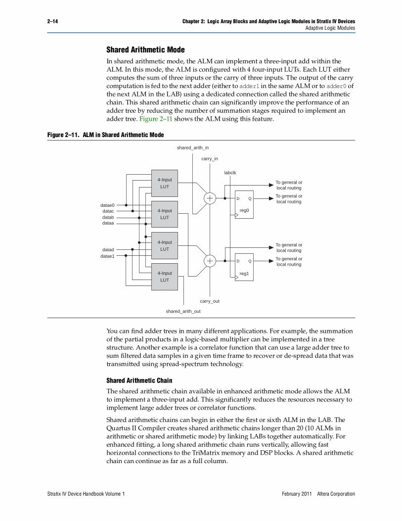
Shared Arithmetic ModeIn shared arithmetic mode, the ALM can implement a three-input add within the ALM. In this mode, the ALM is configured with 4 four-input LUTs. Each LUT either computes the sum of three inputs or the carry of three inputs. The output of the carry computation is fed to the next adder (either to adder1 in the same ALM or to adder0 of the next ALM in the LAB) using a dedicated connection called the shared arithmetic chain. This shared arithmetic chain can significantly improve the performance of an adder tree by reducing the number of summation stages required to implement an adder tree. Figure 2–11 shows the ALM using this feature.
You can find adder trees in many different applications. For example, the summation of the partial products in a logic-based multiplier can be implemented in a tree structure. Another example is a correlator function that can use a large adder tree to sum filtered data samples in a given time frame to recover or de-spread data that was transmitted using spread-spectrum technology.
Shared Arithmetic Chain
The shared arithmetic chain available in enhanced arithmetic mode allows the ALM to implement a three-input add. This significantly reduces the resources necessary to implement large adder trees or correlator functions.
Shared arithmetic chains can begin in either the first or sixth ALM in the LAB. The Quartus II Compiler creates shared arithmetic chains longer than 20 (10 ALMs in arithmetic or shared arithmetic mode) by linking LABs together automatically. For enhanced fitting, a long shared arithmetic chain runs vertically, allowing fast horizontal connections to the TriMatrix memory and DSP blocks. A shared arithmetic chain can continue as far as a full column.
Figure 2–11. ALM in Shared Arithmetic Mode
datae0
carry_in
shared_arith_in
shared_arith_out
carry_out
dataadatabdatac
dataddatae1
D Q
D Q
To general orlocal routing
To general orlocal routing
reg0
reg1
To general orlocal routing
To general orlocal routing
4-Input
LUT
4-Input
LUT
4-Input
LUT
4-Input
LUT
labclk
Stratix IV Device Handbook Volume 1 February 2011 Altera Corporation
Chapter 2: Logic Array Blocks and Adaptive Logic Modules in Stratix IV Devices 2–15Adaptive Logic Modules
Similar to the carry chains, the top and bottom halves of shared arithmetic chains in alternate LAB columns can be bypassed. This capability allows the shared arithmetic chain to cascade through half of the ALMs in an LAB while leaving the other half available for narrower fan-in functionality. Every other LAB column is top-half by-passable, while the other LAB columns are bottom-half by-passable.
For more information about the shared arithmetic chain interconnect, refer to “ALM Interconnects” on page 2–18.
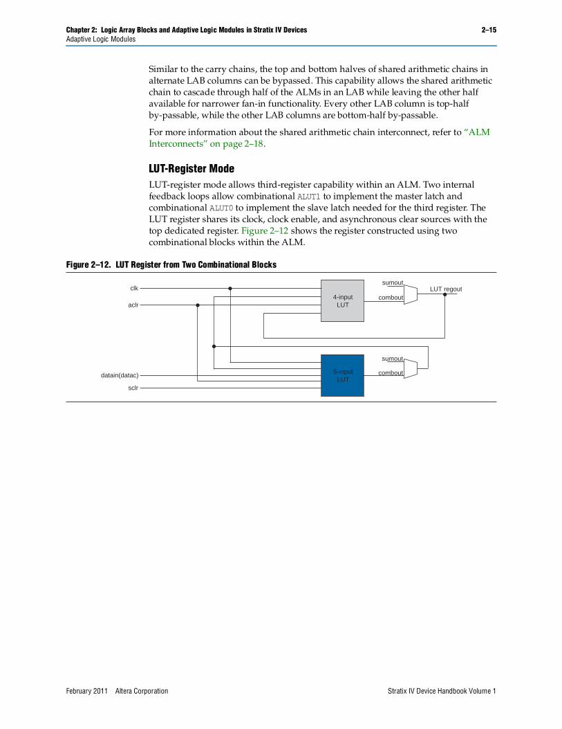
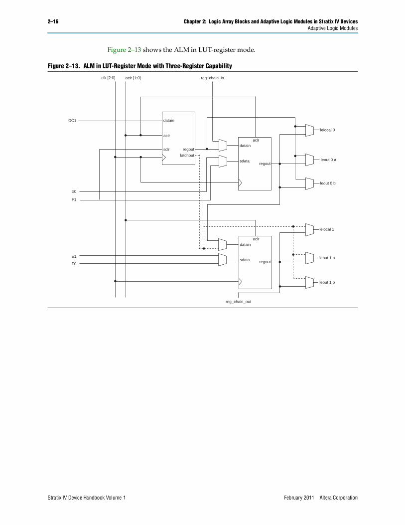
LUT-Register ModeLUT-register mode allows third-register capability within an ALM. Two internal feedback loops allow combinational ALUT1 to implement the master latch and combinational ALUT0 to implement the slave latch needed for the third register. The LUT register shares its clock, clock enable, and asynchronous clear sources with the top dedicated register. Figure 2–12 shows the register constructed using two combinational blocks within the ALM.
Figure 2–12. LUT Register from Two Combinational Blocks
4-inputLUT
5-inputLUT
clk
aclr
datain(datac)
sclr
sumout
comboutLUT regout
sumout
combout
February 2011 Altera Corporation Stratix IV Device Handbook Volume 1
2–16 Chapter 2: Logic Array Blocks and Adaptive Logic Modules in Stratix IV DevicesAdaptive Logic Modules
Figure 2–13 shows the ALM in LUT-register mode.
Figure 2–13. ALM in LUT-Register Mode with Three-Register Capability
datain
aclr
sclr regout
latchout
datain
sdataregout
aclr
datain
sdata regout
aclr
DC1
E0
F1
E1
F0
clk [2:0] aclr [1:0] reg_chain_in
lelocal 0
leout 0 a
leout 0 b
reg_chain_out
lelocal 1
leout 1 a
leout 1 b
Stratix IV Device Handbook Volume 1 February 2011 Altera Corporation
Chapter 2: Logic Array Blocks and Adaptive Logic Modules in Stratix IV Devices 2–17Adaptive Logic Modules
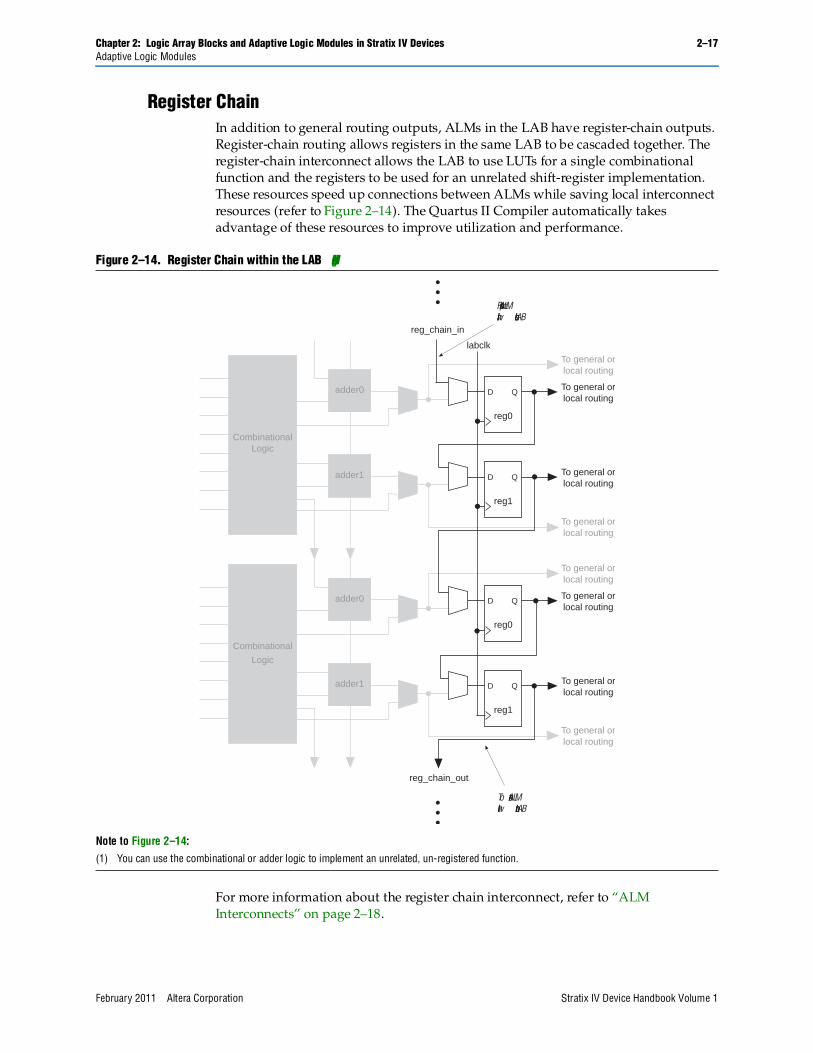
Register ChainIn addition to general routing outputs, ALMs in the LAB have register-chain outputs. Register-chain routing allows registers in the same LAB to be cascaded together. The register-chain interconnect allows the LAB to use LUTs for a single combinational function and the registers to be used for an unrelated shift-register implementation. These resources speed up connections between ALMs while saving local interconnect resources (refer to Figure 2–14). The Quartus II Compiler automatically takes advantage of these resources to improve utilization and performance.
For more information about the register chain interconnect, refer to “ALM Interconnects” on page 2–18.
Figure 2–14. Register Chain within the LAB (Note 1)
Note to Figure 2–14:(1) You can use the combinational or adder logic to implement an unrelated, un-registered function.
D QTo general orlocal routing
reg0
To general orlocal routing
reg_chain_in
adder0
D QTo general orlocal routing
reg1
To general orlocal routing
adder1
D QTo general orlocal routing
reg0
To general orlocal routing
reg_chain_out
adder0
D QTo general orlocal routing
reg1
To general orlocal routing
adder1
From previous ALMwithin the LAB
To next ALMwithin the LAB
Combinational
Logic
CombinationalLogic
labclk
February 2011 Altera Corporation Stratix IV Device Handbook Volume 1
2–18 Chapter 2: Logic Array Blocks and Adaptive Logic Modules in Stratix IV DevicesAdaptive Logic Modules
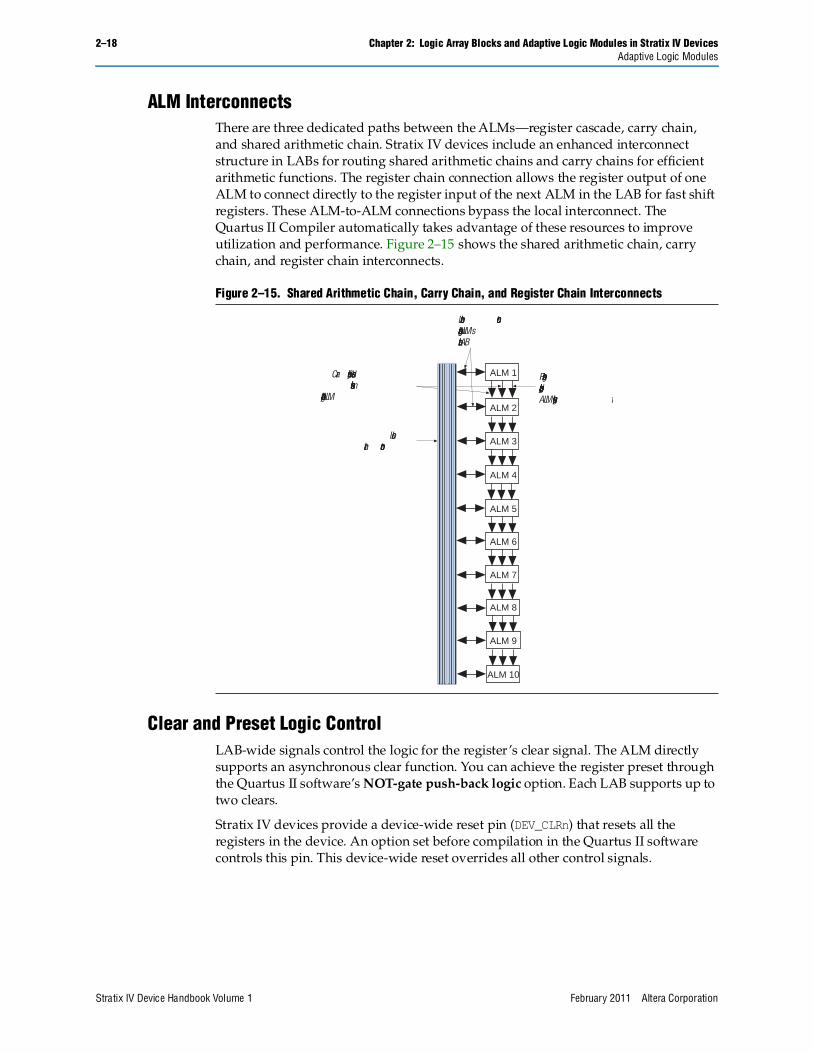
ALM InterconnectsThere are three dedicated paths between the ALMs—register cascade, carry chain, and shared arithmetic chain. Stratix IV devices include an enhanced interconnect structure in LABs for routing shared arithmetic chains and carry chains for efficient arithmetic functions. The register chain connection allows the register output of one ALM to connect directly to the register input of the next ALM in the LAB for fast shift registers. These ALM-to-ALM connections bypass the local interconnect. The Quartus II Compiler automatically takes advantage of these resources to improve utilization and performance. Figure 2–15 shows the shared arithmetic chain, carry chain, and register chain interconnects.
Clear and Preset Logic ControlLAB-wide signals control the logic for the register ’s clear signal. The ALM directly supports an asynchronous clear function. You can achieve the register preset through the Quartus II software’s NOT-gate push-back logic option. Each LAB supports up to two clears.
Stratix IV devices provide a device-wide reset pin (DEV_CLRn) that resets all the registers in the device. An option set before compilation in the Quartus II software controls this pin. This device-wide reset overrides all other control signals.
Figure 2–15. Shared Arithmetic Chain, Carry Chain, and Register Chain Interconnects
ALM 1
ALM 2
ALM 3
ALM 4
ALM 5
ALM 6
Carry chain & sharedarithmetic chain
routing to adjacent ALM
Localinterconnect
Register chainrouting to adjacentALM's register input
Local interconnectrouting among ALMsin the LAB
ALM 7
ALM 8
ALM 9
ALM 10
Stratix IV Device Handbook Volume 1 February 2011 Altera Corporation
Chapter 2: Logic Array Blocks and Adaptive Logic Modules in Stratix IV Devices 2–19Document Revision History
LAB Power Management Techniques The following techniques are used to manage static and dynamic power consumption within the LAB:
■ To save AC power, the Quartus II software forces all adder inputs low when ALM adders are not in use.
■ Stratix IV LABs operate in high-performance mode or low-power mode. The Quartus II software automatically chooses the appropriate mode for the LAB, based on the design, to optimize speed versus leakage trade-offs.
■ Clocks represent a significant portion of dynamic power consumption due to their high switching activity and long paths. The LAB clock that distributes a clock signal to registers within an LAB is a significant contributor to overall clock power consumption. Each LAB’s clock and clock enable signal are linked. For example, a combinational ALUT or register in a particular LAB using the labclk1 signal also uses the labclkena1 signal. To disable LAB-wide clock power consumption without disabling the entire clock tree, use LAB-wide clock enable to gate the LAB-wide clock. The Quartus II software automatically promotes register-level clock enable signals to the LAB-level. All registers within the LAB that share a common clock and clock enable are controlled by a shared, gated clock. To take advantage of these clock enables, use a clock-enable construct in your HDL code for the registered logic.
f For more information about implementing static and dynamic power consumption within the LAB, refer to the Power Optimization chapter in volume 2 of the Quartus II Handbook.
Document Revision HistoryTable 2–1 lists the revision history for this chapter.
Table 2–1. Document Revision History
Date Version Changes
February 2011 3.1
■ Updated Figure 2–6.
■ Applied new template.
■ Minor text edits.
November 2009 3.0■ Updated graphics.
■ Minor text edits.
June 2009 2.2
■ Removed the Conclusion section.
■ Added introductory sentences to improve search ability.
■ Minor text edits.
March 2009 2.1 Removed “Referenced Documents” section.
November 2008 2.0■ Updated Figure 2–6.
■ Made minor editorial changes.
May 2008 1.0 Initial release.
February 2011 Altera Corporation Stratix IV Device Handbook Volume 1

2–20 Chapter 2: Logic Array Blocks and Adaptive Logic Modules in Stratix IV DevicesDocument Revision History
Stratix IV Device Handbook Volume 1 February 2011 Altera Corporation