Embed Size (px)
Citation preview

ni.com/awr
OverviewLoad-pull analysis is one of the key design techniques in amplifi er design and is often used for determining an appropriate load. Amplifi ers
can be designed more effi ciently when using load-pull techniques. The following three examples, extracted from a technical seminar
presented at the Microwave Workshops & Exhibition in Yokohama, Japan, focus on the load-pull analysis capability within Microwave
Offi ce circuit design software for analyzing the impact of terminating impedance on device performance, as well as introducing the
utilization and optimization of electromagnetic (EM) fi eld analysis using AXIEM 3D planar EM software to model the impedance matching
structure.
Load-Pull AnalysisThe NI AWR software load-pull analysis function sweeps the terminating source and load impedances on the respective input and output
sides of the transistors. This enables constant performance contours to be drawn on a Smith chart, thereby showing what load should be
connected so as to optimize the transistor performance (Figure 1).
The load-pull analysis not only specifi es a particular set of load-pull contours (or overlapping contours), but the software can also calculate
and plot a contour for multiple (combined) design criteria, providing the performance characteristics in cases where a matching circuit is
connected and enabling designers to execute a more realistic analysis.
Application Example
Load-Pull Analysis Using NI AWR Software
Figure 1: The red line indicates range within which gain is at 18.5 and PAE at 6
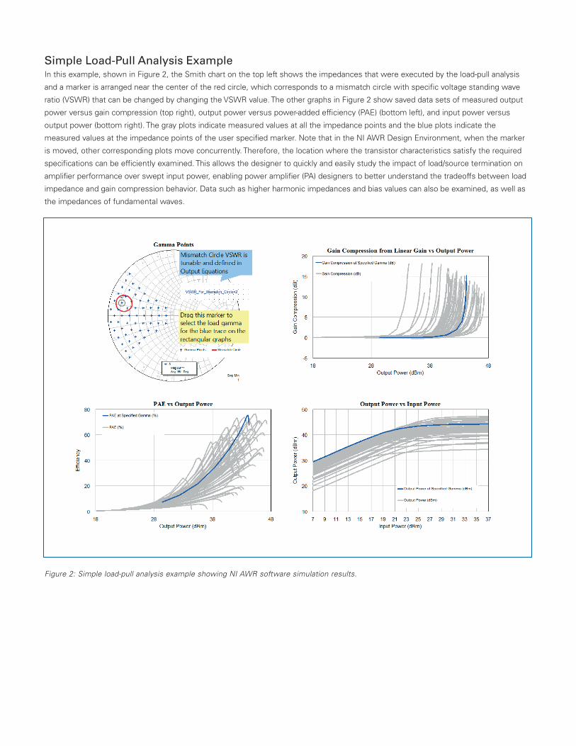
Simple Load-Pull Analysis Example In this example, shown in Figure 2, the Smith chart on the top left shows the impedances that were executed by the load-pull analysis
and a marker is arranged near the center of the red circle, which corresponds to a mismatch circle with specific voltage standing wave
ratio (VSWR) that can be changed by changing the VSWR value. The other graphs in Figure 2 show saved data sets of measured output
power versus gain compression (top right), output power versus power-added efficiency (PAE) (bottom left), and input power versus
output power (bottom right). The gray plots indicate measured values at all the impedance points and the blue plots indicate the
measured values at the impedance points of the user specified marker. Note that in the NI AWR Design Environment, when the marker
is moved, other corresponding plots move concurrently. Therefore, the location where the transistor characteristics satisfy the required
specifications can be efficiently examined. This allows the designer to quickly and easily study the impact of load/source termination on
amplifier performance over swept input power, enabling power amplifier (PA) designers to better understand the tradeoffs between load
impedance and gain compression behavior. Data such as higher harmonic impedances and bias values can also be examined, as well as
the impedances of fundamental waves.
Figure 2: Simple load-pull analysis example showing NI AWR software simulation results.

Matching Circuit ExampleIn this example, shown in Figure 3, the device was terminated in matching network based on a microstrip transmission line transformer
representing a more realistic matching circuit. Since the improved load-pull analysis function can execute load-pull analysis with multiple
frequencies, the optimum matching can be examined over any frequency band using a matching circuit with frequency characteristics.
The Smith chart in the top left of Figure 3 shows the impedances that were executed by load-pull analysis, indicating a contour line
(orange) where 45 dBm output power can be obtained, a contour line (green) where 70 percent PAE can be obtained, the common range
(red), and impedances (blue) of the matching circuit that is connected.
The layout of the matching circuit and the circuit diagram are shown in the lower half and the performance characteristics of the device
with the matching network are shown on the top right. The parameters of the matching circuit can be adjusted by a tuner, which adjusts
the transmission line width/length, thereby impacting the electrical characteristics of the transmission line transformer. The analysis result
and the circuit diagram layout can then be examined while checking the multiple frequency characteristics on the Smith chart.
Figure 3: Matching circuit load-pull example showing matching network schematic and layout, as well as simulated results.

Circuit Optimization ExampleIn this example, shown in Figure 4, circuit optimization that relies upon EM fi eld analysis using AXIEM 3D planar EM tool is explored. In a
layered structure, such as a monolithic microwave integrated circuit (MMIC)/substrate/module, the effect of the structure can be
calculated effi ciently by using an EM analysis engine such as AXIEM. By using optimization that leverages EM analysis, a more accurate
representation of the matching network impedance can be achieved. While EM analysis is often used in design verifi cation after the fi nal
design has been achieved, this example illustrates the accuracy of EM analysis when used earlier in the design process during fi nal
optimization of the matching circuit.
Looking again at Figure 4, it shows the schematic, layout, and swept (input power) results of the actual project. The left bottom is the
EM structure that was created through EM extraction technology. In this case, the EM structure was automatically updated and
analyzed as a single unit, depending on the parameter changes during optimization that occurred in the individual distributed circuit
models in the schematic.
Figure 4: NI AWR Design Environment depicting schematic, layout, 3D layout, and resultant power out and PAE across frequencies.

Additionally, the output matching circuit for the transistor model was created based on the measured load-pull fi le in order to investigate
current distribution through the matching structure and to understand the behavior of the design and investigate the reliability. NI AWR
Design Environment provides the capability to show the current distribution with circuit elements. The matching circuit was connected to
the transistor model, the EM analysis was performed, and the current distribution observed (Figure 5).
Specifi cally within Figure 5, the graph at the right shows the analysis results. Blue is output power, pink is PAE, the solid line is the
load-pull analysis result, and the broken line is the analysis result using the model. The diagram on the left shows current distribution.
Although there is a slight difference between PAE by the load-pull analysis and PAE by the analysis conducted using the model, the
accuracy can be improved by including the impact of the impedance at harmonic frequencies during the load-pull analysis. The current
distribution not only shows the distribution of the current when power is input to the EM fi eld structure, but also shows the current
distribution obtained by taking into account the effect of the capacitor and other parts that are connected on the circuit diagram.
ConclusionNI AWR Design Environment is an complete high-frequency design platform. The underlying technologies of circuits, layouts, and
electromagnetic fi eld analysis are integrated and linked effectively within the platform. Many features are added with each new version
and functions such as load-pull analysis have been added to it to improve the effi ciency of amplifi er design and support the design of
highly complex amplifi ers. With NI AWR software, designers are able to not only examine the characteristics of transistors by load-pull
analysis, but also to examine the matching circuit and its effects in the electromagnetic fi eld and, moreover, move quickly to subsequent
design processes.
Additional Notes: Further details on load-pull analysis can be found in the application note, “NI AWR Design Environment Load-Pull Simulation Supports the
Design of Wideband High-Effi ciency PAs.”
Figure 5: Current distribution of matching circuit example shown in Figure 4.
©2016 National Instruments. All rights reserved. AWR, AXIEM, Microwave Offi ce, National Instruments, NI, and ni.com are trademarks of National Instruments. Other product and company names listed are trademarks or trade names of their respective companies. AN-M-LDPL-EMP-2016.3.2
Many thanks to Tsutomu
Sugawara, AWR Group, NI
for his contributions to this
application note.