Embed Size (px)
Citation preview
Product
Folder
Sample &Buy
Technical
Documents
Tools &
Software
Support &Community
LM193-N, LM2903-N, LM293-N, LM393-NSNOSBJ6F –OCTOBER 1999–REVISED DECEMBER 2014
LMx93-N, LM2903-N Low-Power, Low-Offset Voltage, Dual Comparators1 Features 3 Description
The LM193-N series consists of two independent1• Wide Supply
precision voltage comparators with an offset voltage– Voltage Range: 2.0 V to 36 V specification as low as 2.0 mV max for two– Single or Dual Supplies: ±1.0 V to ±18 V comparators which were designed specifically to
operate from a single power supply over a wide range• Very Low Supply Current Drain (0.4 mA) —of voltages. Operation from split power supplies isIndependent of Supply Voltagealso possible and the low power supply current drain• Low Input Biasing Current: 25 nA is independent of the magnitude of the power supply
• Low Input Offset Current: ±5 nA voltage. These comparators also have a uniquecharacteristic in that the input common-mode voltage• Maximum Offset voltage: ±3 mVrange includes ground, even though operated from a• Input Common-Mode Voltage Range Includes single power supply voltage.GroundApplication areas include limit comparators, simple• Differential Input Voltage Range Equal to theanalog to digital converters; pulse, squarewave andPower Supply Voltagetime delay generators; wide range VCO; MOS clock
• Low Output Saturation Voltage: 250 mV at 4 mA timers; multivibrators and high voltage digital logic• Output Voltage Compatible with TTL, DTL, ECL, gates. The LM193-N series was designed to directly
interface with TTL and CMOS. When operated fromMOS and CMOS logic systemsboth plus and minus power supplies, the LM19-N• Available in the 8-Bump (12 mil) DSBGA Packageseries will directly interface with MOS logic where
• See AN-1112 (SNVA009) for DSBGA their low power drain is a distinct advantage overConsiderations standard comparators.
• Advantages The LM393 and LM2903 parts are available in TI’s– High Precision Comparators innovative thin DSBGA package with 8 (12 mil) large
bumps.– Reduced VOS Drift Over Temperature– Eliminates Need for Dual Supplies Device Information(1)– Allows Sensing Near Ground PART NUMBER PACKAGE BODY SIZE (NOM)– Compatible with All Forms of Logic LM193-N
TO-99 (8) 9.08 mm x 9.08 mm– Power Drain Suitable for Battery Operation LM293-NLM393-N
SOIC (8) 4.90 mm x 3.91 mm2 ApplicationsLM2903-N
• Battery powered applications (1) For all available packages, see the orderable addendum atthe end of the datasheet.• Industrial applications
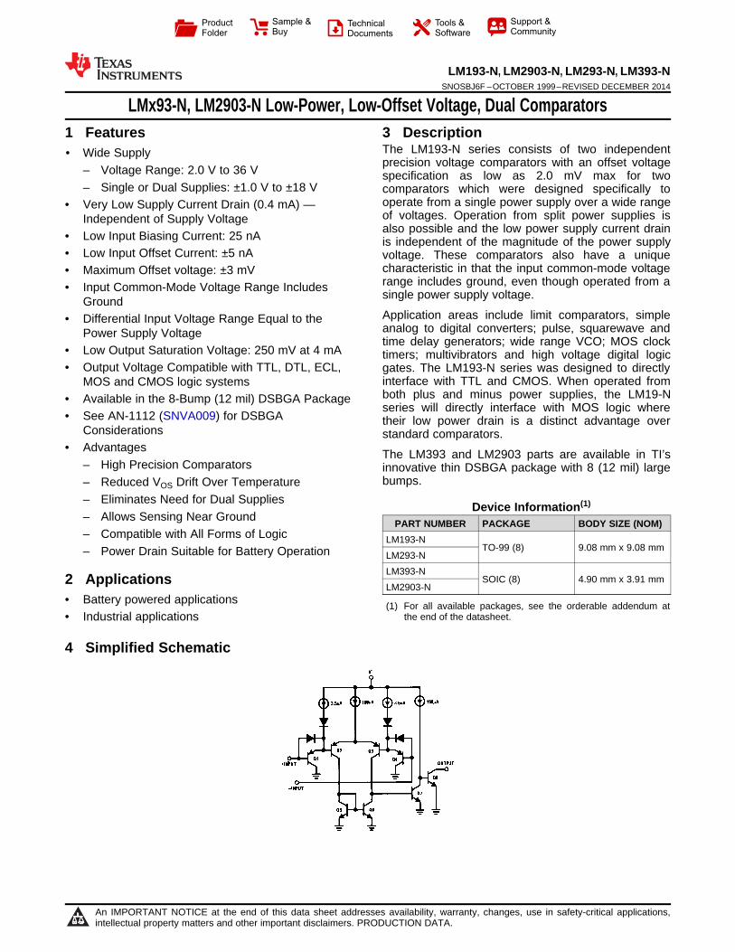
4 Simplified Schematic
1
An IMPORTANT NOTICE at the end of this data sheet addresses availability, warranty, changes, use in safety-critical applications,intellectual property matters and other important disclaimers. PRODUCTION DATA.
LM193-N, LM2903-N, LM293-N, LM393-NSNOSBJ6F –OCTOBER 1999–REVISED DECEMBER 2014 www.ti.com
Table of Contents1 Features .................................................................. 1 8 Detailed Description ............................................ 10
8.1 Overview ................................................................. 102 Applications ........................................................... 18.2 Functional Block Diagram ....................................... 103 Description ............................................................. 18.3 Feature Description................................................. 104 Simplified Schematic............................................. 18.4 Device Functional Modes........................................ 105 Revision History..................................................... 2
9 Application and Implementation ........................ 116 Pin Configuration and Functions ......................... 39.1 Application Information............................................ 117 Specifications......................................................... 49.2 Typical Applications ................................................ 117.1 Absolute Maximum Ratings ..................................... 4
10 Power Supply Recommendations ..................... 187.2 ESD Ratings ............................................................ 411 Layout................................................................... 187.3 Recommended Operating Conditions....................... 4
11.1 Layout Guidelines ................................................. 187.4 Thermal Information .................................................. 511.2 Layout Example .................................................... 187.5 Electrical Characteristics: LM193A V+= 5 V, TA =
25°C ........................................................................... 5 12 Device and Documentation Support ................. 197.6 Electrical Characteristics: LM193A (V+ = 5 V) ......... 5 12.1 Related Links ........................................................ 197.7 Electrical Characteristics: LMx93 and LM2903 V+= 5 12.2 Trademarks ........................................................... 19
V, TA = 25°C .............................................................. 6 12.3 Electrostatic Discharge Caution............................ 197.8 Electrical Characteristics: LMx93 and LM2903 (V+ = 12.4 Glossary ................................................................ 19
5 V) (1) ......................................................................... 7 13 Mechanical, Packaging, and Orderable7.9 Typical Characteristics: LMx93 and LM193A............ 8 Information ........................................................... 197.10 Typical Characteristics: LM2903 ............................ 9
5 Revision HistoryNOTE: Page numbers for previous revisions may differ from page numbers in the current version.
Changes from Revision E (March 2013) to Revision F Page
• Added Pin Configuration and Functions section, ESD Ratings table, Feature Description section, Device FunctionalModes, Application and Implementation section, Power Supply Recommendations section, Layout section, Deviceand Documentation Support section, and Mechanical, Packaging, and Orderable Information section .............................. 1
Changes from Revision D (March 2013) to Revision E Page
• Changed layout of National Data Sheet to TI format ............................................................................................................ 1
2 Submit Documentation Feedback Copyright © 1999–2014, Texas Instruments Incorporated
Product Folder Links: LM193-N LM2903-N LM293-N LM393-N

LM193-N, LM2903-N, LM293-N, LM393-Nwww.ti.com SNOSBJ6F –OCTOBER 1999–REVISED DECEMBER 2014
6 Pin Configuration and Functions
8-Pin TO-99 8-Pin CDIP, PDIP, SOICLMC Package P and D Package
Top View Top View
8-Pin DSBGAYZR Package
Top View
Pin FunctionsPIN
NO. I/O DESCRIPTIONNAME PDIP/SOIC/ DSBGATO-99OUTA 1 A1 O Output, Channel A-INA 2 B1 I Inverting Input, Channel A+INA 3 C1 I Noninverting Input, Channel AGND 4 C2 P Ground+INB 5 C3 I Noninverting Input, Channel B-INB 6 B3 I Inverting Input, Channel BOUTB 7 A3 O Output, Channel BV+ 8 A2 P Positive power supply
Copyright © 1999–2014, Texas Instruments Incorporated Submit Documentation Feedback 3
Product Folder Links: LM193-N LM2903-N LM293-N LM393-N

LM193-N, LM2903-N, LM293-N, LM393-NSNOSBJ6F –OCTOBER 1999–REVISED DECEMBER 2014 www.ti.com
7 Specifications
7.1 Absolute Maximum Ratingsover operating free-air temperature range (unless otherwise noted) (1) (2) (3)
MIN MAX UNITDifferential Input Voltage (4) 36 VInput Voltage −0.3 36 VInput Current (VIN<−0.3 V) (5) 50 mAPower PDIP 780 mWDissipation (6)
TO-99 660 mWSOIC 510 mWDSBGA 568 mW
Output Short-Circuit to Ground (7) Continuous
Lead Temperature (Soldering, 10 seconds) 260 °CSoldering PDIP Package Soldering (10 seconds) 260 °CInformation SOIC Package Vapor Phase (60 seconds) 215 °C
Infrared (15 seconds) 220 °CStorage temperature, Tstg -65 150 °C
(1) Absolute Maximum Ratings indicate limits beyond which damage may occur. Recommended Operating Conditions indicate conditionsfor which the device is intended to be functional, but specific performance is not guaranteed. For guaranteed specifications and testconditions, see the Electrical Characteristics.
(2) Refer to RETS193AX for LM193AH military specifications and to RETS193X for LM193H military specifications.(3) If Military/Aerospace specified devices are required, please contact the TI Sales Office/Distributors for availability and specifications.(4) Positive excursions of input voltage may exceed the power supply level. As long as the other voltage remains within the common-mode
range, the comparator will provide a proper output state. The low input voltage state must not be less than −0.3V (or 0.3V below themagnitude of the negative power supply, if used).
(5) This input current will only exist when the voltage at any of the input leads is driven negative. It is due to the collector-base junction ofthe input PNP transistors becoming forward biased and thereby acting as input diode clamps. In addition to this diode action, there isalso lateral NPN parasitic transistor action on the IC chip. This transistor action can cause the output voltages of the comparators to goto the V+ voltage level (or to ground for a large overdrive) for the time duration that an input is driven negative. This is not destructiveand normal output states will re-establish when the input voltage, which was negative, again returns to a value greater than −0.3V.
(6) For operating at high temperatures, the LM393 and LM2903 must be derated based on a 125°C maximum junction temperature and athermal resistance of 170°C/W which applies for the device soldered in a printed circuit board, operating in a still air ambient. TheLM193/LM193A/LM293 must be derated based on a 150°C maximum junction temperature. The low bias dissipation and the “ON-OFF”characteristic of the outputs keeps the chip dissipation very small (PD≤100 mW), provided the output transistors are allowed to saturate.
(7) Short circuits from the output to V+ can cause excessive heating and eventual destruction. When considering short circuits to ground,the maximum output current is approximately 20 mA independent of the magnitude of V+.
7.2 ESD RatingsVALUE UNIT
V(ESD) Electrostatic discharge Human-body model (HBM), per ANSI/ESDA/JEDEC JS-001 (1) ±1300 V
(1) JEDEC document JEP155 states that 500-V HBM allows safe manufacturing with a standard ESD control process.
7.3 Recommended Operating Conditionsover operating free-air temperature range (unless otherwise noted)
MIN NOM MAX UNITSupply Voltage (V+) - Single Supply 2.0 36 VSupply Voltage (V+) - Dual Supply ±1.0 ±18 VOperating Input Voltage on (VIN pin) 0 (V+) -1.5V VOperating junction temperature, TJ : LM193/LM193A -55 125 °COperating junction temperature, TJ : LM2903 -40 85 °COperating junction temperature, TJ : LM293 -25 85 °COperating junction temperature, TJ : LM393 0 70 °C
4 Submit Documentation Feedback Copyright © 1999–2014, Texas Instruments Incorporated
Product Folder Links: LM193-N LM2903-N LM293-N LM393-N

LM193-N, LM2903-N, LM293-N, LM393-Nwww.ti.com SNOSBJ6F –OCTOBER 1999–REVISED DECEMBER 2014
7.4 Thermal InformationLMx93
THERMAL METRIC (1) TO-99 UNIT8 PINS
RθJA Junction-to-ambient thermal resistance 170 °C/W
(1) For more information about traditional and new thermal metrics, see the IC Package Thermal Metrics application report, SPRA953.
7.5 Electrical Characteristics: LM193A V+= 5 V, TA = 25°CUnless otherwise stated.
LM193APARAMETER TEST CONDITIONS UNIT
MIN TYP MAXInput Offset Voltage See (1). 1.0 2.0 mVInput Bias Current IIN(+) or IIN(−) with Output In Linear Range, VCM = 0 V (2) 25 100 nAInput Offset Current IIN(+)−IIN(−) VCM = 0 V 3.0 25 nAInput Common Mode Voltage Range V+ = 30 V (3) 0 V+−1.5 VSupply Current RL=∞ V+=5 V 0.4 1 mA
V+=36 V 1 2.5 mAVoltage Gain RL≥15 kΩ, V+=15 V 50 200 V/mV
VO = 1 V to 11 VLarge Signal Response Time VIN=TTL Logic Swing, VREF=1.4 V 300 ns
VRL=5V, RL=5.1 kΩResponse Time VRL=5V, RL=5.1 kΩ (4) 1.3 μsOutput Sink Current VIN(−)=1V, VIN(+)=0, VO≈1.5 V 6.0 16 mASaturation Voltage VIN(−)=1V, VIN(+)=0, ISINK≤4 mA 250 400 mVOutput Leakage Current VIN(−)=0, VIN(+)=1V, VO=5 V 0.1 nA
(1) At output switch point, VO≃1.4V, RS= 0 Ω with V+ from 5V to 30V; and over the full input common-mode range (0V to V+−1.5V), at 25°C.(2) The direction of the input current is out of the IC due to the PNP input stage. This current is essentially constant, independent of the
state of the output so no loading change exists on the reference or input lines.(3) The input common-mode voltage or either input signal voltage should not be allowed to go negative by more than 0.3V. The upper end
of the common-mode voltage range is V+−1.5 V at 25°C, but either or both inputs can go to 36 V without damage, independent of themagnitude of V+.
(4) The response time specified is for a 100 mV input step with 5 mV overdrive. For larger overdrive signals 300 ns can be obtained, seeLMx93 and LM193A Typical Characteristics .
7.6 Electrical Characteristics: LM193A (V+ = 5 V) (1)
LM193APARAMETER TEST CONDITIONS UNIT
MIN TYP MAXInput Offset Voltage See (2) 4.0 mVInput Offset Current IIN(+)−IIN(−), VCM=0 V 100 nAInput Bias Current IIN(+) or IIN(−) with Output in Linear Range, VCM=0 V (3) 300 nAInput Common Mode Voltage Range V+=30 V (4) 0 V+−2.0 VSaturation Voltage VIN(−)=1V, VIN(+)=0, ISINK≤4 mA 700 mVOutput Leakage Current VIN(−)=0, VIN(+)=1V, VO=30 V 1.0 μADifferential Input Voltage Keep All VIN's≥0 V (or V−, if Used), (5) 36 V
(1) These specifications are limited to −55°C≤TA≤+125°C, for the LM193/LM193A. With the LM293 all temperature specifications are limitedto −25°C≤TA≤+85°C and the LM393 temperature specifications are limited to 0°C≤TA≤+70°C. The LM2903 is limited to−40°C≤TA≤+85°C.
(2) At output switch point, VO≃1.4V, RS= 0 Ω with V+ from 5V to 30V; and over the full input common-mode range (0V to V+−1.5V), at 25°C.(3) The direction of the input current is out of the IC due to the PNP input stage. This current is essentially constant, independent of the
state of the output so no loading change exists on the reference or input lines.(4) The input common-mode voltage or either input signal voltage should not be allowed to go negative by more than 0.3V. The upper end
of the common-mode voltage range is V+−1.5 V at 25°C, but either or both inputs can go to 36 V without damage, independent of themagnitude of V+.
(5) Positive excursions of input voltage may exceed the power supply level. As long as the other voltage remains within the common-moderange, the comparator will provide a proper output state. The low input voltage state must not be less than −0.3V (or 0.3V below themagnitude of the negative power supply, if used).
Copyright © 1999–2014, Texas Instruments Incorporated Submit Documentation Feedback 5
Product Folder Links: LM193-N LM2903-N LM293-N LM393-N

LM193-N, LM2903-N, LM293-N, LM393-NSNOSBJ6F –OCTOBER 1999–REVISED DECEMBER 2014 www.ti.com
7.7 Electrical Characteristics: LMx93 and LM2903 V+= 5 V, TA = 25°CUnless otherwise stated.
LM193-N LM293-N, LM393- LM2903-NNPARAMETER TEST CONDITIONS UNIT
MIN TYP MAX MIN TYP MAX MIN TYP MAXInput Offset Voltage See (1) 1.0 5.0 1.0 5.0 2.0 7.0 mVInput Bias Current IIN(+) or IIN(−) with Output In 25 100 25 250 25 250 nA
Linear Range, VCM = 0 V (2)
Input Offset Current IIN(+)−IIN(−) VCM = 0 V 3.0 25 5.0 50 5.0 50 nAInput Common Mode V+ = 30 V (3) 0 V+−1. 0 V+−1 0 V+−1 VVoltage Range 5 .5 .5Supply Current RL=∞ V+=5 V 0.4 1 0.4 1 0.4 1.0 mA
V+=36 V 1 2.5 1 2.5 1 2.5 mAVoltage Gain RL≥15 kΩ, V+=15 V 50 200 50 200 25 100 V/mV
VO = 1 V to 11 VLarge Signal Response VIN=TTL Logic Swing, VREF=1.4 V 300 300 300 nsTime VRL=5 V, RL=5.1 kΩResponse Time VRL=5 V, RL=5.1 kΩ (4) 1.3 1.3 1.5 μsOutput Sink Current VIN(−)=1 V, VIN(+)=0, VO≤1.5 V 6.0 16 6.0 16 6.0 16 mASaturation Voltage VIN(−)=1 V, VIN(+)=0, ISINK≤4 mA 250 400 250 400 250 400 mVOutput Leakage Current VIN(−)=0, VIN(+)=1V, VO=5 V 0.1 0.1 0.1 nA
(1) At output switch point, VO≃1.4V, RS= 0 Ω with V+ from 5V to 30V; and over the full input common-mode range (0V to V+−1.5V), at 25°C.(2) The direction of the input current is out of the IC due to the PNP input stage. This current is essentially constant, independent of the
state of the output so no loading change exists on the reference or input lines.(3) The input common-mode voltage or either input signal voltage should not be allowed to go negative by more than 0.3V. The upper end
of the common-mode voltage range is V+−1.5 V at 25°C, but either or both inputs can go to 36 V without damage, independent of themagnitude of V+.
(4) The response time specified is for a 100 mV input step with 5 mV overdrive. For larger overdrive signals 300 ns can be obtained, seeLMx93 and LM193A Typical Characteristics .
6 Submit Documentation Feedback Copyright © 1999–2014, Texas Instruments Incorporated
Product Folder Links: LM193-N LM2903-N LM293-N LM393-N
LM193-N, LM2903-N, LM293-N, LM393-Nwww.ti.com SNOSBJ6F –OCTOBER 1999–REVISED DECEMBER 2014
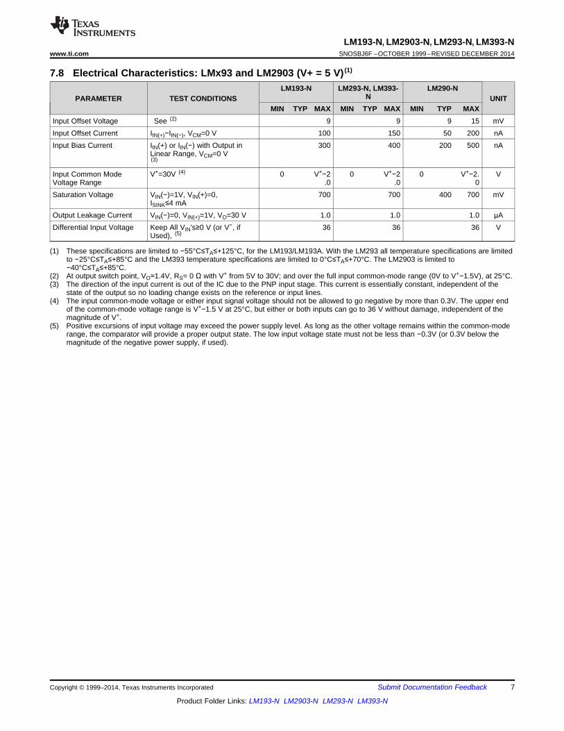
7.8 Electrical Characteristics: LMx93 and LM2903 (V+ = 5 V) (1)
LM193-N LM293-N, LM393- LM290-NNPARAMETER TEST CONDITIONS UNIT
MIN TYP MAX MIN TYP MAX MIN TYP MAXInput Offset Voltage See (2) 9 9 9 15 mVInput Offset Current IIN(+)−IIN(−), VCM=0 V 100 150 50 200 nAInput Bias Current IIN(+) or IIN(−) with Output in 300 400 200 500 nA
Linear Range, VCM=0 V(3)
Input Common Mode V+=30V (4) 0 V+−2 0 V+−2 0 V+−2. VVoltage Range .0 .0 0Saturation Voltage VIN(−)=1V, VIN(+)=0, 700 700 400 700 mV
ISINK≤4 mAOutput Leakage Current VIN(−)=0, VIN(+)=1V, VO=30 V 1.0 1.0 1.0 μADifferential Input Voltage Keep All VIN's≥0 V (or V−, if 36 36 36 V
Used), (5)
(1) These specifications are limited to −55°C≤TA≤+125°C, for the LM193/LM193A. With the LM293 all temperature specifications are limitedto −25°C≤TA≤+85°C and the LM393 temperature specifications are limited to 0°C≤TA≤+70°C. The LM2903 is limited to−40°C≤TA≤+85°C.
(2) At output switch point, VO≃1.4V, RS= 0 Ω with V+ from 5V to 30V; and over the full input common-mode range (0V to V+−1.5V), at 25°C.(3) The direction of the input current is out of the IC due to the PNP input stage. This current is essentially constant, independent of the
state of the output so no loading change exists on the reference or input lines.(4) The input common-mode voltage or either input signal voltage should not be allowed to go negative by more than 0.3V. The upper end
of the common-mode voltage range is V+−1.5 V at 25°C, but either or both inputs can go to 36 V without damage, independent of themagnitude of V+.
(5) Positive excursions of input voltage may exceed the power supply level. As long as the other voltage remains within the common-moderange, the comparator will provide a proper output state. The low input voltage state must not be less than −0.3V (or 0.3V below themagnitude of the negative power supply, if used).
Copyright © 1999–2014, Texas Instruments Incorporated Submit Documentation Feedback 7
Product Folder Links: LM193-N LM2903-N LM293-N LM393-N

LM193-N, LM2903-N, LM293-N, LM393-NSNOSBJ6F –OCTOBER 1999–REVISED DECEMBER 2014 www.ti.com
7.9 Typical Characteristics: LMx93 and LM193A
Figure 1. Supply Current Figure 2. Input Current
Figure 4. Response Time for Various InputFigure 3. Output Saturation VoltageOverdrives—Negative Transition
Figure 5. Response Time for Various Input Overdrives—Positive Transition
8 Submit Documentation Feedback Copyright © 1999–2014, Texas Instruments Incorporated
Product Folder Links: LM193-N LM2903-N LM293-N LM393-N

LM193-N, LM2903-N, LM293-N, LM393-Nwww.ti.com SNOSBJ6F –OCTOBER 1999–REVISED DECEMBER 2014
7.10 Typical Characteristics: LM2903
Figure 7. Input CurrentFigure 6. Supply Current
Figure 9. Response Time for Various InputOverdrives—Negative TransitionFigure 8. Output Saturation Voltage
Figure 10. Response Time for Various Input Overdrives—Positive Transition
Copyright © 1999–2014, Texas Instruments Incorporated Submit Documentation Feedback 9
Product Folder Links: LM193-N LM2903-N LM293-N LM393-N

LM193-N, LM2903-N, LM293-N, LM393-NSNOSBJ6F –OCTOBER 1999–REVISED DECEMBER 2014 www.ti.com
8 Detailed Description
8.1 OverviewThe LM139 provides two independently functioning, high-precision, low VOS drift, low input bias currentcomparators in a single package. The low power consumption of 0.4mA at 5V and the 2.0V supply operationmakes the LM139 suitable for battery powered applications.
8.2 Functional Block Diagram
Figure 11. Basic Comparator
8.3 Feature DescriptionThe input bias current of 25 nA enables the LM193 to use even very high impedance nodes as inputs. Thedifferential voltage input range equals the supply voltage range.
The LM193 can be operated with a single supply, where V+ can be from 2.0 V to 36 V, or in a dual supplyvoltage configuration, where GND pin is used as a V– supply. The supply current draws only 0.4 mA for bothcomparators.
The output of each comparator in the LM193 is the open collector of a grounded-emitter NPN output transistorwhich can typically draw up to 16mA.
8.4 Device Functional ModesA basic comparator circuit is used for converting analog signals to a digital output. The output is HIGH when thevoltage on the non-inverting (+IN) input is greater than the inverting (-IN) input. The output is LOW when thevoltage on the non-inverting (+IN) input is less than the inverting (-IN) input. The inverting input (-IN) is alsocommonly referred to as the "reference" or "VREF" input. All pins of any unused comparators should be tied tothe negative supply.
10 Submit Documentation Feedback Copyright © 1999–2014, Texas Instruments Incorporated
Product Folder Links: LM193-N LM2903-N LM293-N LM393-N

LM193-N, LM2903-N, LM293-N, LM393-Nwww.ti.com SNOSBJ6F –OCTOBER 1999–REVISED DECEMBER 2014
9 Application and Implementation
NOTEInformation in the following applications sections is not part of the TI componentspecification, and TI does not warrant its accuracy or completeness. TI’s customers areresponsible for determining suitability of components for their purposes. Customers shouldvalidate and test their design implementation to confirm system functionality.
9.1 Application Information
The LM193 series are high gain, wide bandwidth devices which, like most comparators, can easily oscillate if theoutput lead is inadvertently allowed to capacitively couple to the inputs via stray capacitance. This shows up onlyduring the output voltage transition intervals as the comparator change states. Power supply bypassing is notrequired to solve this problem. Standard PC board layout is helpful as it reduces stray input-output coupling.Reducing the input resistors to < 10 kΩ reduces the feedback signal levels and finally, adding even a smallamount (1.0 to 10 mV) of positive feedback (hysteresis) causes such a rapid transition that oscillations due tostray feedback are not possible. Simply socketing the IC and attaching resistors to the pins will cause input-output oscillations during the small transition intervals unless hysteresis is used. If the input signal is a pulsewaveform, with relatively fast rise and fall times, hysteresis is not required.
All input pins of any unused comparators should be tied to the negative supply.
The bias network of the LM193 series establishes a drain current which is independent of the magnitude of thepower supply voltage over the range of from 2.0 VDC to 30 VDC.
The differential input voltage may be larger than V+ without damaging the deviceTypical Applications . Protectionshould be provided to prevent the input voltages from going negative more than −0.3 VDC (at 25°C). An inputclamp diode can be used as shown in Typical Applications .
The output of the LM193 series is the uncommitted collector of a grounded-emitter NPN output transistor. Manycollectors can be tied together to provide an output OR'ing function. An output pullup resistor can be connectedto any available power supply voltage within the permitted supply voltage range and there is no restriction on thisvoltage due to the magnitude of the voltage which is applied to the V+ terminal of the LM193 package. Theoutput can also be used as a simple SPST switch to ground (when a pullup resistor is not used). The amount ofcurrent which the output device can sink is limited by the drive available (which is independent of V+) and the βof this device. When the maximum current limit is reached (approximately 16mA), the output transistor will comeout of saturation and the output voltage will rise very rapidly. The output saturation voltage is limited by theapproximately 60Ω rSAT of the output transistor. The low offset voltage of the output transistor (1.0mV) allows theoutput to clamp essentially to ground level for small load currents.
9.2 Typical Applications
9.2.1 Basic Comparator
Figure 12. Basic Comparator
9.2.1.1 Design RequirementsThe basic usage of a comparator is to indicate when a specific analog signal has exceeded some predefinedthreshold. In this application, the negative input (IN–) is tied to a reference voltage, and the positive input (IN+) isconnected to the input signal. The output is pulled up with a resistor to the logic supply voltage, V+ with a pullupresistor.
For an example application, the supply voltage is 5V. The input signal varies between 1 V and 3 V, and we wantto know when the input exceeds 2.5 V±1%. The supply current draw should not exceed 1 mA.Copyright © 1999–2014, Texas Instruments Incorporated Submit Documentation Feedback 11
Product Folder Links: LM193-N LM2903-N LM293-N LM393-N
LM193-N, LM2903-N, LM293-N, LM393-NSNOSBJ6F –OCTOBER 1999–REVISED DECEMBER 2014 www.ti.com
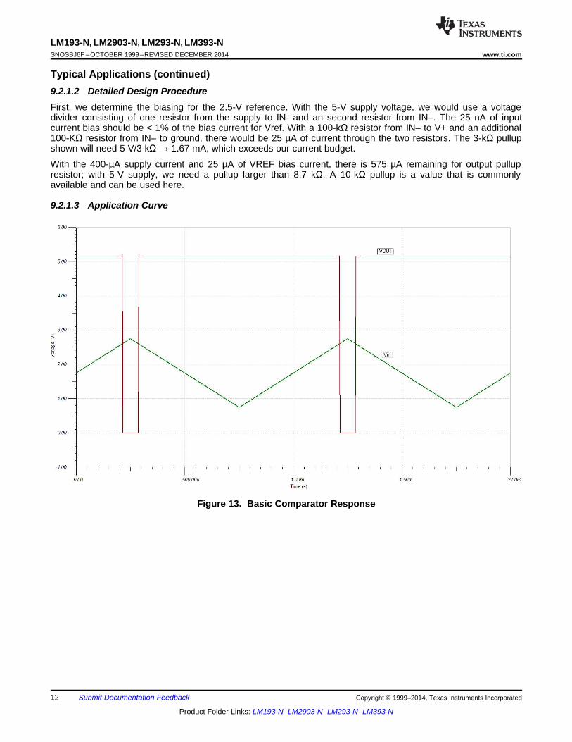
Typical Applications (continued)9.2.1.2 Detailed Design ProcedureFirst, we determine the biasing for the 2.5-V reference. With the 5-V supply voltage, we would use a voltagedivider consisting of one resistor from the supply to IN- and an second resistor from IN–. The 25 nA of inputcurrent bias should be < 1% of the bias current for Vref. With a 100-kΩ resistor from IN– to V+ and an additional100-KΩ resistor from IN– to ground, there would be 25 µA of current through the two resistors. The 3-kΩ pullupshown will need 5 V/3 kΩ → 1.67 mA, which exceeds our current budget.
With the 400-µA supply current and 25 µA of VREF bias current, there is 575 µA remaining for output pullupresistor; with 5-V supply, we need a pullup larger than 8.7 kΩ. A 10-kΩ pullup is a value that is commonlyavailable and can be used here.
9.2.1.3 Application Curve
Figure 13. Basic Comparator Response
12 Submit Documentation Feedback Copyright © 1999–2014, Texas Instruments Incorporated
Product Folder Links: LM193-N LM2903-N LM293-N LM393-N

LM193-N, LM2903-N, LM293-N, LM393-Nwww.ti.com SNOSBJ6F –OCTOBER 1999–REVISED DECEMBER 2014
Typical Applications (continued)9.2.2 System Examples
9.2.2.1 Split-Supply Application
(V+=-15 VDC and V-=-15 VDC)
Figure 14. MOS Clock Driver
9.2.2.2 V+ = 5.0 VDC Application Circuits
Figure 15. Driving CMOS Figure 16. Driving TTL
* For large ratios of R1/R2,D1 can be omitted.
Figure 17. Squarewave Oscillator Figure 18. Pulse Generator
Copyright © 1999–2014, Texas Instruments Incorporated Submit Documentation Feedback 13
Product Folder Links: LM193-N LM2903-N LM293-N LM393-N
LM193-N, LM2903-N, LM293-N, LM393-NSNOSBJ6F –OCTOBER 1999–REVISED DECEMBER 2014 www.ti.com
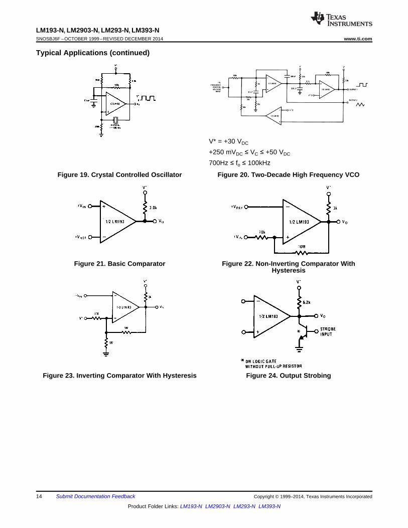
Typical Applications (continued)
V* = +30 VDC
+250 mVDC ≤ VC ≤ +50 VDC
700Hz ≤ fo ≤ 100kHz
Figure 19. Crystal Controlled Oscillator Figure 20. Two-Decade High Frequency VCO
Figure 21. Basic Comparator Figure 22. Non-Inverting Comparator WithHysteresis
Figure 23. Inverting Comparator With Hysteresis Figure 24. Output Strobing
14 Submit Documentation Feedback Copyright © 1999–2014, Texas Instruments Incorporated
Product Folder Links: LM193-N LM2903-N LM293-N LM393-N

LM193-N, LM2903-N, LM293-N, LM393-Nwww.ti.com SNOSBJ6F –OCTOBER 1999–REVISED DECEMBER 2014
Typical Applications (continued)
Figure 25. And Gate Figure 26. Or Gate
Figure 27. Large Fan-In and Gate Figure 28. Limit Comparator
Figure 29. Comparing Input Voltages of Opposite Figure 30. Oring the OutputsPolarity
Copyright © 1999–2014, Texas Instruments Incorporated Submit Documentation Feedback 15
Product Folder Links: LM193-N LM2903-N LM293-N LM393-N

LM193-N, LM2903-N, LM293-N, LM393-NSNOSBJ6F –OCTOBER 1999–REVISED DECEMBER 2014 www.ti.com
Typical Applications (continued)
Figure 31. Zero Crossing Detector (Single Power Figure 32. One-Shot MultivibratorSupply)
Figure 33. Bi-Stable Multivibrator Figure 34. One-Shot Multivibrator With Input LockOut
Figure 35. Zero Crossing Detector Figure 36. Comparator With a Negative Reference
16 Submit Documentation Feedback Copyright © 1999–2014, Texas Instruments Incorporated
Product Folder Links: LM193-N LM2903-N LM293-N LM393-N

LM193-N, LM2903-N, LM293-N, LM393-Nwww.ti.com SNOSBJ6F –OCTOBER 1999–REVISED DECEMBER 2014
Typical Applications (continued)
Figure 37. Time Delay Generator
Copyright © 1999–2014, Texas Instruments Incorporated Submit Documentation Feedback 17
Product Folder Links: LM193-N LM2903-N LM293-N LM393-N

LM193-N, LM2903-N, LM293-N, LM393-NSNOSBJ6F –OCTOBER 1999–REVISED DECEMBER 2014 www.ti.com
10 Power Supply RecommendationsEven in low frequency applications, the LM139-N can have internal transients which are extremely quick. For thisreason, bypassing the power supply with 1.0μF to ground will provide improved performance; the supply bypasscapacitor should be placed as close as possible to the supply pin and have a solid connection to ground. Thebypass capacitor should have a low ESR and also a SRF greater than 50MHz.
11 Layout
11.1 Layout GuidelinesTry to minimize parasitic impedances on the inputs to avoid oscillation. Any positive feedback used as hysteresisshould place the feedback components as close as possible to the input pins. Care should be taken to ensurethat the output pins do not couple to the inputs. This can occur through capacitive coupling if the traces are tooclose and lead to oscillations on the output. The optimum placement for the bypass capacitor is closest to the V+and ground pins. Take care to minimize the loop area formed by the bypass capacitor connection between V+and ground. The ground pin should be connected to the PCB ground plane at the pin of the device. Thefeedback components should be placed as close to the device as possible minimizing strays.
11.2 Layout Example
Figure 38. Layout Example
18 Submit Documentation Feedback Copyright © 1999–2014, Texas Instruments Incorporated
Product Folder Links: LM193-N LM2903-N LM293-N LM393-N
LM193-N, LM2903-N, LM293-N, LM393-Nwww.ti.com SNOSBJ6F –OCTOBER 1999–REVISED DECEMBER 2014
12 Device and Documentation Support
12.1 Related LinksThe table below lists quick access links. Categories include technical documents, support and communityresources, tools and software, and quick access to sample or buy.
Table 1. Related LinksTECHNICAL TOOLS & SUPPORT &PARTS PRODUCT FOLDER SAMPLE & BUY DOCUMENTS SOFTWARE COMMUNITY
LM193-N Click here Click here Click here Click here Click hereLM2903-N Click here Click here Click here Click here Click hereLM293-N Click here Click here Click here Click here Click hereLM393-N Click here Click here Click here Click here Click here
12.2 TrademarksAll trademarks are the property of their respective owners.
12.3 Electrostatic Discharge CautionThese devices have limited built-in ESD protection. The leads should be shorted together or the device placed in conductive foamduring storage or handling to prevent electrostatic damage to the MOS gates.
12.4 GlossarySLYZ022 — TI Glossary.
This glossary lists and explains terms, acronyms, and definitions.
13 Mechanical, Packaging, and Orderable InformationThe following pages include mechanical, packaging, and orderable information. This information is the mostcurrent data available for the designated devices. This data is subject to change without notice and revision ofthis document. For browser-based versions of this data sheet, refer to the left-hand navigation.
Copyright © 1999–2014, Texas Instruments Incorporated Submit Documentation Feedback 19
Product Folder Links: LM193-N LM2903-N LM293-N LM393-N

PACKAGE OPTION ADDENDUM
www.ti.com 21-Nov-2017
Addendum-Page 1
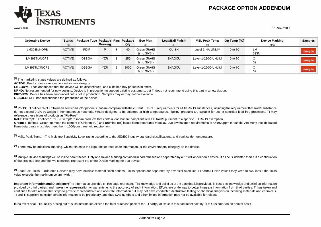
PACKAGING INFORMATION
Orderable Device Status(1)
Package Type PackageDrawing
Pins PackageQty
Eco Plan(2)
Lead/Ball Finish(6)
MSL Peak Temp(3)
Op Temp (°C) Device Marking(4/5)
Samples
LM193AH ACTIVE TO-99 LMC 8 500 TBD Call TI Call TI -55 to 125 ( LM193AH, LM193AH )
LM193AH/NOPB ACTIVE TO-99 LMC 8 500 Green (RoHS& no Sb/Br)
Call TI Level-1-NA-UNLIM -55 to 125 ( LM193AH, LM193AH )
LM193H ACTIVE TO-99 LMC 8 500 TBD Call TI Call TI -55 to 125 ( LM193H, LM193H)
LM193H/NOPB ACTIVE TO-99 LMC 8 500 Green (RoHS& no Sb/Br)
Call TI Level-1-NA-UNLIM -55 to 125 ( LM193H, LM193H)
LM2903ITL/NOPB ACTIVE DSBGA YZR 8 250 Green (RoHS& no Sb/Br)
SNAGCU Level-1-260C-UNLIM -40 to 85 C03
LM2903ITLX/NOPB ACTIVE DSBGA YZR 8 3000 Green (RoHS& no Sb/Br)
SNAGCU Level-1-260C-UNLIM -40 to 85 C03
LM2903M ACTIVE SOIC D 8 95 TBD Call TI Call TI -40 to 85 LM2903M
LM2903M/NOPB ACTIVE SOIC D 8 95 Green (RoHS& no Sb/Br)
CU SN Level-1-260C-UNLIM -40 to 85 LM2903M
LM2903MX LIFEBUY SOIC D 8 2500 TBD Call TI Call TI -40 to 85 LM2903M
LM2903MX/NOPB ACTIVE SOIC D 8 2500 Green (RoHS& no Sb/Br)
CU SN Level-1-260C-UNLIM -40 to 85 LM2903M
LM2903N/NOPB ACTIVE PDIP P 8 40 Green (RoHS& no Sb/Br)
CU SN Level-1-NA-UNLIM -40 to 85 LM2903N
LM293H ACTIVE TO-99 LMC 8 500 TBD Call TI Call TI -25 to 85 ( LM293H, LM293H)
LM293H/NOPB ACTIVE TO-99 LMC 8 500 Green (RoHS& no Sb/Br)
Call TI Level-1-NA-UNLIM -25 to 85 ( LM293H, LM293H)
LM393M NRND SOIC D 8 95 TBD Call TI Call TI 0 to 70 LM393M
LM393M/NOPB ACTIVE SOIC D 8 95 Green (RoHS& no Sb/Br)
CU SN Level-1-260C-UNLIM 0 to 70 LM393M
LM393MX NRND SOIC D 8 2500 TBD Call TI Call TI 0 to 70 LM393M
LM393MX/NOPB ACTIVE SOIC D 8 2500 Green (RoHS& no Sb/Br)
CU SN Level-1-260C-UNLIM 0 to 70 LM393M
PACKAGE OPTION ADDENDUM
www.ti.com 21-Nov-2017
Addendum-Page 2
Orderable Device Status(1)
Package Type PackageDrawing
Pins PackageQty
Eco Plan(2)
Lead/Ball Finish(6)
MSL Peak Temp(3)
Op Temp (°C) Device Marking(4/5)
Samples
LM393N/NOPB ACTIVE PDIP P 8 40 Green (RoHS& no Sb/Br)
CU SN Level-1-NA-UNLIM 0 to 70 LM393N
LM393TL/NOPB ACTIVE DSBGA YZR 8 250 Green (RoHS& no Sb/Br)
SNAGCU Level-1-260C-UNLIM 0 to 70 C02
LM393TLX/NOPB ACTIVE DSBGA YZR 8 3000 Green (RoHS& no Sb/Br)
SNAGCU Level-1-260C-UNLIM 0 to 70 C02
(1) The marketing status values are defined as follows:ACTIVE: Product device recommended for new designs.LIFEBUY: TI has announced that the device will be discontinued, and a lifetime-buy period is in effect.NRND: Not recommended for new designs. Device is in production to support existing customers, but TI does not recommend using this part in a new design.PREVIEW: Device has been announced but is not in production. Samples may or may not be available.OBSOLETE: TI has discontinued the production of the device.
(2) RoHS: TI defines "RoHS" to mean semiconductor products that are compliant with the current EU RoHS requirements for all 10 RoHS substances, including the requirement that RoHS substancedo not exceed 0.1% by weight in homogeneous materials. Where designed to be soldered at high temperatures, "RoHS" products are suitable for use in specified lead-free processes. TI mayreference these types of products as "Pb-Free".RoHS Exempt: TI defines "RoHS Exempt" to mean products that contain lead but are compliant with EU RoHS pursuant to a specific EU RoHS exemption.Green: TI defines "Green" to mean the content of Chlorine (Cl) and Bromine (Br) based flame retardants meet JS709B low halogen requirements of <=1000ppm threshold. Antimony trioxide basedflame retardants must also meet the <=1000ppm threshold requirement.
(3) MSL, Peak Temp. - The Moisture Sensitivity Level rating according to the JEDEC industry standard classifications, and peak solder temperature.
(4) There may be additional marking, which relates to the logo, the lot trace code information, or the environmental category on the device.
(5) Multiple Device Markings will be inside parentheses. Only one Device Marking contained in parentheses and separated by a "~" will appear on a device. If a line is indented then it is a continuationof the previous line and the two combined represent the entire Device Marking for that device.
(6) Lead/Ball Finish - Orderable Devices may have multiple material finish options. Finish options are separated by a vertical ruled line. Lead/Ball Finish values may wrap to two lines if the finishvalue exceeds the maximum column width.
Important Information and Disclaimer:The information provided on this page represents TI's knowledge and belief as of the date that it is provided. TI bases its knowledge and belief on informationprovided by third parties, and makes no representation or warranty as to the accuracy of such information. Efforts are underway to better integrate information from third parties. TI has taken andcontinues to take reasonable steps to provide representative and accurate information but may not have conducted destructive testing or chemical analysis on incoming materials and chemicals.TI and TI suppliers consider certain information to be proprietary, and thus CAS numbers and other limited information may not be available for release.
In no event shall TI's liability arising out of such information exceed the total purchase price of the TI part(s) at issue in this document sold by TI to Customer on an annual basis.
PACKAGE OPTION ADDENDUM
www.ti.com 21-Nov-2017
Addendum-Page 3
OTHER QUALIFIED VERSIONS OF LM2903-N, LM293-N :
• Automotive: LM2903-Q1
• Enhanced Product: LM293-EP
NOTE: Qualified Version Definitions:
• Automotive - Q100 devices qualified for high-reliability automotive applications targeting zero defects
• Enhanced Product - Supports Defense, Aerospace and Medical Applications

TAPE AND REEL INFORMATION
*All dimensions are nominal
Device PackageType
PackageDrawing
Pins SPQ ReelDiameter
(mm)
ReelWidth
W1 (mm)
A0(mm)
B0(mm)
K0(mm)
P1(mm)
W(mm)
Pin1Quadrant
LM2903ITL/NOPB DSBGA YZR 8 250 178.0 8.4 1.7 1.7 0.76 4.0 8.0 Q1
LM2903ITLX/NOPB DSBGA YZR 8 3000 178.0 8.4 1.7 1.7 0.76 4.0 8.0 Q1
LM2903MX SOIC D 8 2500 330.0 12.4 6.5 5.4 2.0 8.0 12.0 Q1
LM2903MX/NOPB SOIC D 8 2500 330.0 12.4 6.5 5.4 2.0 8.0 12.0 Q1
LM393MX SOIC D 8 2500 330.0 12.4 6.5 5.4 2.0 8.0 12.0 Q1
LM393MX/NOPB SOIC D 8 2500 330.0 12.4 6.5 5.4 2.0 8.0 12.0 Q1
LM393TL/NOPB DSBGA YZR 8 250 178.0 8.4 1.7 1.7 0.76 4.0 8.0 Q1
LM393TLX/NOPB DSBGA YZR 8 3000 178.0 8.4 1.7 1.7 0.76 4.0 8.0 Q1
PACKAGE MATERIALS INFORMATION
www.ti.com 9-Oct-2014
Pack Materials-Page 1
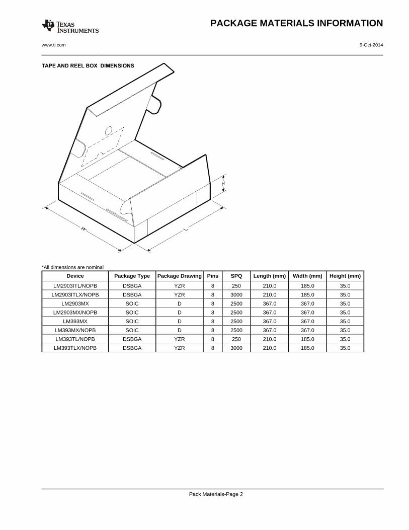
*All dimensions are nominal
Device Package Type Package Drawing Pins SPQ Length (mm) Width (mm) Height (mm)
LM2903ITL/NOPB DSBGA YZR 8 250 210.0 185.0 35.0
LM2903ITLX/NOPB DSBGA YZR 8 3000 210.0 185.0 35.0
LM2903MX SOIC D 8 2500 367.0 367.0 35.0
LM2903MX/NOPB SOIC D 8 2500 367.0 367.0 35.0
LM393MX SOIC D 8 2500 367.0 367.0 35.0
LM393MX/NOPB SOIC D 8 2500 367.0 367.0 35.0
LM393TL/NOPB DSBGA YZR 8 250 210.0 185.0 35.0
LM393TLX/NOPB DSBGA YZR 8 3000 210.0 185.0 35.0
PACKAGE MATERIALS INFORMATION
www.ti.com 9-Oct-2014
Pack Materials-Page 2
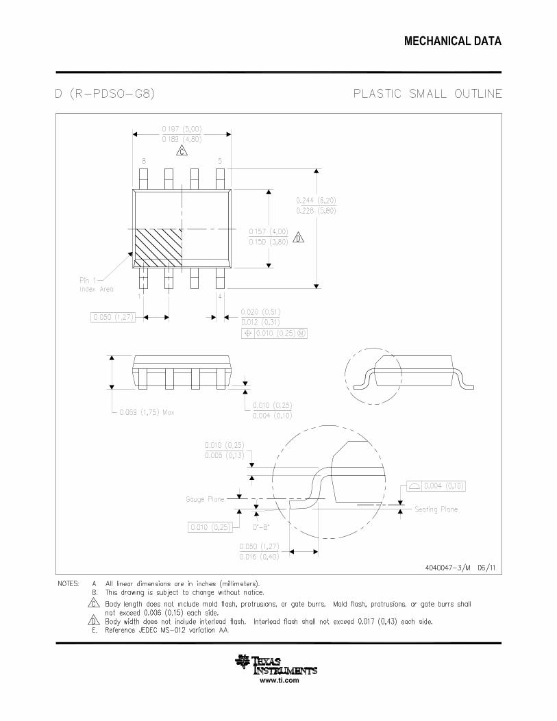


MECHANICAL DATA
YZR0008xxx
www.ti.com
TLA08XXX (Rev C)
0.600±0.075D
E
A. All linear dimensions are in millimeters. Dimensioning and tolerancing per ASME Y14.5M-1994.B. This drawing is subject to change without notice.
NOTES:
4215045/A 12/12
D: Max =
E: Max =
1.54 mm, Min =
1.54 mm, Min =
1.479 mm
1.479 mm
IMPORTANT NOTICE
Texas Instruments Incorporated (TI) reserves the right to make corrections, enhancements, improvements and other changes to itssemiconductor products and services per JESD46, latest issue, and to discontinue any product or service per JESD48, latest issue. Buyersshould obtain the latest relevant information before placing orders and should verify that such information is current and complete.TI’s published terms of sale for semiconductor products (http://www.ti.com/sc/docs/stdterms.htm) apply to the sale of packaged integratedcircuit products that TI has qualified and released to market. Additional terms may apply to the use or sale of other types of TI products andservices.Reproduction of significant portions of TI information in TI data sheets is permissible only if reproduction is without alteration and isaccompanied by all associated warranties, conditions, limitations, and notices. TI is not responsible or liable for such reproduceddocumentation. Information of third parties may be subject to additional restrictions. Resale of TI products or services with statementsdifferent from or beyond the parameters stated by TI for that product or service voids all express and any implied warranties for theassociated TI product or service and is an unfair and deceptive business practice. TI is not responsible or liable for any such statements.Buyers and others who are developing systems that incorporate TI products (collectively, “Designers”) understand and agree that Designersremain responsible for using their independent analysis, evaluation and judgment in designing their applications and that Designers havefull and exclusive responsibility to assure the safety of Designers' applications and compliance of their applications (and of all TI productsused in or for Designers’ applications) with all applicable regulations, laws and other applicable requirements. Designer represents that, withrespect to their applications, Designer has all the necessary expertise to create and implement safeguards that (1) anticipate dangerousconsequences of failures, (2) monitor failures and their consequences, and (3) lessen the likelihood of failures that might cause harm andtake appropriate actions. Designer agrees that prior to using or distributing any applications that include TI products, Designer willthoroughly test such applications and the functionality of such TI products as used in such applications.TI’s provision of technical, application or other design advice, quality characterization, reliability data or other services or information,including, but not limited to, reference designs and materials relating to evaluation modules, (collectively, “TI Resources”) are intended toassist designers who are developing applications that incorporate TI products; by downloading, accessing or using TI Resources in anyway, Designer (individually or, if Designer is acting on behalf of a company, Designer’s company) agrees to use any particular TI Resourcesolely for this purpose and subject to the terms of this Notice.TI’s provision of TI Resources does not expand or otherwise alter TI’s applicable published warranties or warranty disclaimers for TIproducts, and no additional obligations or liabilities arise from TI providing such TI Resources. TI reserves the right to make corrections,enhancements, improvements and other changes to its TI Resources. TI has not conducted any testing other than that specificallydescribed in the published documentation for a particular TI Resource.Designer is authorized to use, copy and modify any individual TI Resource only in connection with the development of applications thatinclude the TI product(s) identified in such TI Resource. NO OTHER LICENSE, EXPRESS OR IMPLIED, BY ESTOPPEL OR OTHERWISETO ANY OTHER TI INTELLECTUAL PROPERTY RIGHT, AND NO LICENSE TO ANY TECHNOLOGY OR INTELLECTUAL PROPERTYRIGHT OF TI OR ANY THIRD PARTY IS GRANTED HEREIN, including but not limited to any patent right, copyright, mask work right, orother intellectual property right relating to any combination, machine, or process in which TI products or services are used. Informationregarding or referencing third-party products or services does not constitute a license to use such products or services, or a warranty orendorsement thereof. Use of TI Resources may require a license from a third party under the patents or other intellectual property of thethird party, or a license from TI under the patents or other intellectual property of TI.TI RESOURCES ARE PROVIDED “AS IS” AND WITH ALL FAULTS. TI DISCLAIMS ALL OTHER WARRANTIES ORREPRESENTATIONS, EXPRESS OR IMPLIED, REGARDING RESOURCES OR USE THEREOF, INCLUDING BUT NOT LIMITED TOACCURACY OR COMPLETENESS, TITLE, ANY EPIDEMIC FAILURE WARRANTY AND ANY IMPLIED WARRANTIES OFMERCHANTABILITY, FITNESS FOR A PARTICULAR PURPOSE, AND NON-INFRINGEMENT OF ANY THIRD PARTY INTELLECTUALPROPERTY RIGHTS. TI SHALL NOT BE LIABLE FOR AND SHALL NOT DEFEND OR INDEMNIFY DESIGNER AGAINST ANY CLAIM,INCLUDING BUT NOT LIMITED TO ANY INFRINGEMENT CLAIM THAT RELATES TO OR IS BASED ON ANY COMBINATION OFPRODUCTS EVEN IF DESCRIBED IN TI RESOURCES OR OTHERWISE. IN NO EVENT SHALL TI BE LIABLE FOR ANY ACTUAL,DIRECT, SPECIAL, COLLATERAL, INDIRECT, PUNITIVE, INCIDENTAL, CONSEQUENTIAL OR EXEMPLARY DAMAGES INCONNECTION WITH OR ARISING OUT OF TI RESOURCES OR USE THEREOF, AND REGARDLESS OF WHETHER TI HAS BEENADVISED OF THE POSSIBILITY OF SUCH DAMAGES.Unless TI has explicitly designated an individual product as meeting the requirements of a particular industry standard (e.g., ISO/TS 16949and ISO 26262), TI is not responsible for any failure to meet such industry standard requirements.Where TI specifically promotes products as facilitating functional safety or as compliant with industry functional safety standards, suchproducts are intended to help enable customers to design and create their own applications that meet applicable functional safety standardsand requirements. Using products in an application does not by itself establish any safety features in the application. Designers mustensure compliance with safety-related requirements and standards applicable to their applications. Designer may not use any TI products inlife-critical medical equipment unless authorized officers of the parties have executed a special contract specifically governing such use.Life-critical medical equipment is medical equipment where failure of such equipment would cause serious bodily injury or death (e.g., lifesupport, pacemakers, defibrillators, heart pumps, neurostimulators, and implantables). Such equipment includes, without limitation, allmedical devices identified by the U.S. Food and Drug Administration as Class III devices and equivalent classifications outside the U.S.TI may expressly designate certain products as completing a particular qualification (e.g., Q100, Military Grade, or Enhanced Product).Designers agree that it has the necessary expertise to select the product with the appropriate qualification designation for their applicationsand that proper product selection is at Designers’ own risk. Designers are solely responsible for compliance with all legal and regulatoryrequirements in connection with such selection.Designer will fully indemnify TI and its representatives against any damages, costs, losses, and/or liabilities arising out of Designer’s non-compliance with the terms and provisions of this Notice.
Mailing Address: Texas Instruments, Post Office Box 655303, Dallas, Texas 75265Copyright © 2017, Texas Instruments Incorporated


![TROPHY SERIES Comparators - Digi-Key Sheets/Rohm PDFs/LM393...Commercial Grade LM339/393 family : 0[ ] to + 70[ ] Extended Industrial Grade LM2903/2901 family : -40[ ] to +125[ ] 2)](https://img.pdfslide.us/doc/110x75/5e2bc4d09960d870b606c514/trophy-series-comparators-digi-key-sheetsrohm-pdfslm393-commercial-grade.jpg)