Embed Size (px)
Citation preview

V+
IN+
Class ABControl
Bias Control
Copyright © 2016, Texas Instruments Incorporated
V-
SD
IN VBIAS
IN-
IpVBIAS
OUT
(LMV711 ONLY)
Product
Folder
Sample &Buy
Technical
Documents
Tools &
Software
Support &Community
An IMPORTANT NOTICE at the end of this data sheet addresses availability, warranty, changes, use in safety-critical applications,intellectual property matters and other important disclaimers. PRODUCTION DATA.
LMV710-N, LMV711-N, LMV715-NSNOS519K –APRIL 2000–REVISED AUGUST 2016
LMV71x-N Low-Power, RRIO Operational AmplifiersWith High Output Current Drive and Shutdown Option
1
1 Features1• Low Offset Voltage: 3 mV (Maximum)• Gain-Bandwidth Product: 5 MHz (Typical)• Slew Rate: 5 V/µs (Typical)• Space-Saving Packages: 5-Pin and 6-Pin SOT-23• Turnon Time From Shutdown: <10 µs• Industrial Temperature Range: −40°C to 85°C• Supply Current in Shutdown Mode: 0.2 µA
(Typical)• Ensured 2.7-V and 5-V Performance• Unity Gain Stable• Rail-to-Rail Input and Output• Capable of Driving 600-Ω Load
2 Applications• Wireless Phones• GSM, TDMA, and CDMA Power Amp Controls• AGC and RF Power Detectors• Temperature Compensation• Wireless LAN• Bluetooth• HomeRF
3 DescriptionThe LMV710-N, LMV711-N, and LMV715-N areBiCMOS operational amplifiers with a CMOS inputstage. These devices have greater than RR inputcommon mode voltage range, rail-to-rail output andhigh output current drive. They offer a bandwidth of5 MHz and a slew rate of 5 V/µs.
On the LMV711 and LMV715, a separate shutdownpin can be used to disable the device and reducesthe supply current to 0.2 µA (typical). They alsofeature a turnon time of less than 10 µs. It is an idealsolution for power-sensitive applications, such ascellular phone, pager, palm computer, and so forth. Inaddition, once the LMV715 is in shutdown the outputis tri-stated.
The LMV710 is offered in the space-saving, 5-pinSOT-23 package. The LMV711 and LMV715 areoffered in the space saving 6-pin SOT-23 package.
The LMV71x-N devices are designed to meet thedemands of low power, low cost, and small sizerequired by cellular phones and similar battery-powered portable electronics.
Device Information(1)
PART NUMBER PACKAGE BODY SIZE (NOM)LMV710-N SOT-23 (5) 2.92 mm × 1.50 mmLMV711-NLMV715-N SOT-23 (6) 2.92 mm × 1.50 mm
(1) For all available packages, see the orderable addendum atthe end of the data sheet.
Simplified Schematic – LMV711

2
LMV710-N, LMV711-N, LMV715-NSNOS519K –APRIL 2000–REVISED AUGUST 2016 www.ti.com
Product Folder Links: LMV710-N LMV715-N
Submit Documentation Feedback Copyright © 2000–2016, Texas Instruments Incorporated
Table of Contents1 Features .................................................................. 12 Applications ........................................................... 13 Description ............................................................. 14 Revision History..................................................... 25 Pin Configuration and Functions ......................... 36 Specifications......................................................... 4
6.1 Absolute Maximum Ratings ...................................... 46.2 ESD Ratings.............................................................. 46.3 Recommended Operating Conditions....................... 46.4 Thermal Information ................................................. 46.5 Electrical Characteristics – 2.7 V .............................. 56.6 Electrical Characteristics – 3.2 V .............................. 66.7 Electrical Characteristics – 5 V ................................. 66.8 Typical Characteristics .............................................. 8
7 Detailed Description ............................................ 147.1 Overview ................................................................ 147.2 Functional Block Diagram ....................................... 147.3 Feature Description ................................................ 14
7.4 Device Functional Modes ....................................... 168 Application and Implementation ........................ 19
8.1 Application Information............................................ 198.2 Typical Applications ................................................ 19
9 Power Supply Recommendations ...................... 2210 Layout................................................................... 22
10.1 Layout Guidelines ................................................ 2210.2 Layout Example ................................................... 22
11 Device and Documentation Support ................. 2311.1 Device Support .................................................... 2311.2 Documentation Support ....................................... 2311.3 Related Links ........................................................ 2311.4 Receiving Notification of Documentation Updates 2311.5 Community Resources.......................................... 2311.6 Trademarks ........................................................... 2311.7 Electrostatic Discharge Caution............................ 2411.8 Glossary ................................................................ 24
12 Mechanical, Packaging, and OrderableInformation ........................................................... 24
4 Revision HistoryNOTE: Page numbers for previous revisions may differ from page numbers in the current version.
Changes from Revision J (March 2013) to Revision K Page
• Added ESD Ratings table, Feature Description section, Device Functional Modes, Application and Implementationsection, Power Supply Recommendations section, Layout section, Device and Documentation Support section, andMechanical, Packaging, and Orderable Information section .................................................................................................. 1
3
LMV710-N, LMV711-N, LMV715-Nwww.ti.com SNOS519K –APRIL 2000–REVISED AUGUST 2016
Product Folder Links: LMV710-N LMV715-N
Submit Documentation FeedbackCopyright © 2000–2016, Texas Instruments Incorporated
(1) I = Input, O = Output, P = Power
5 Pin Configuration and Functions
LMV710 DBV Package5-Pin SOT-23
Top View
LMV711, LMV715 DBV Package6-Pin SOT-23
Top View
Pin FunctionsPIN
TYPE (1) DESCRIPTIONNAME DBV (5) DBV (6)+IN 3 3 I Noninverting input–IN 4 4 I Inverting inputOutput 1 1 O OutputShutdown — 5 I Active low enable inputV+ 5 6 P Positive supply inputV– 2 2 P Supply negative input

4
LMV710-N, LMV711-N, LMV715-NSNOS519K –APRIL 2000–REVISED AUGUST 2016 www.ti.com
Product Folder Links: LMV710-N LMV715-N
Submit Documentation Feedback Copyright © 2000–2016, Texas Instruments Incorporated
(1) Stresses beyond those listed under Absolute Maximum Ratings may cause permanent damage to the device. These are stress ratingsonly, which do not imply functional operation of the device at these or any other conditions beyond those indicated under RecommendedOperating Conditions. Exposure to absolute-maximum-rated conditions for extended periods may affect device reliability.
(2) If Military/Aerospace specified devices are required, please contact the Texas Instruments Sales Office/ Distributors for availability andspecifications.
(3) Shorting circuit output to V+ will adversely affect reliability.(4) Shorting circuit output to V− will adversely affect reliability.(5) The maximum power dissipation is a function of TJ(MAX), RθJA, and TA. The maximum allowable power dissipation at any ambient
temperature is PD = (TJ(MAX) – T A) / RθJA. All numbers apply for packages soldered directly into a PCB.
6 Specifications
6.1 Absolute Maximum Ratingsover operating free-air temperature range (unless otherwise noted) (1) (2)
MIN MAX UNITDifferential input voltage ±Supply voltageVoltage at input or output pin (V–) − 0.4 (V+) + 0.4 VSupply voltage (V+ - V −) 5.5 VOutput short circuit to V+ See (3)
Output short circuit to V− See (4)
Current at input pin ±10 mAMounting temperature, infrared or convection (20 sec) 235 °CJunction temperature, TJ(MAX)
(5) 150 °CStorage temperature, Tstg –65 150 °C
(1) JEDEC document JEP155 states that 500-V HBM allows safe manufacturing with a standard ESD control process.(2) Human-body model, 1.5 kΩ in series with 100 pF.(3) Machine model, 0 Ω in series with 100 pF.
6.2 ESD RatingsVALUE UNIT
V(ESD) Electrostatic dischargeHuman-body model (HBM) (1) (2) ±2000
VMachine model (MM) (3) ±100
6.3 Recommended Operating Conditionsover operating free-air temperature range (unless otherwise noted)
MIN MAX UNITSupply voltage 2.7 5 VTemperature –40 85 °C
(1) For more information about traditional and new thermal metrics, see the Semiconductor and IC Package Thermal Metrics applicationreport.
6.4 Thermal Information
THERMAL METRIC (1)LMV710-N LMV711-N LMV715-N
UNITDBV (SOT-23) DBV (SOT-23) DBV (SOT-23)5 PINS 6 PINS 6 PINS
RθJA Junction-to-ambient thermal resistance 265 265 265 °C/WRθJC(top) Junction-to-case (top) thermal resistance 131.6 139 156.6 °C/WRθJB Junction-to-board thermal resistance 35.1 38.5 32.8 °C/WψJT Junction-to-top characterization parameter 22.2 28.6 34 °C/WψJB Junction-to-board characterization parameter 34.5 37.9 32.2 °C/WRθJC(bot) Junction-to-case (bottom) thermal resistance — — — °C/W

5
LMV710-N, LMV711-N, LMV715-Nwww.ti.com SNOS519K –APRIL 2000–REVISED AUGUST 2016
Product Folder Links: LMV710-N LMV715-N
Submit Documentation FeedbackCopyright © 2000–2016, Texas Instruments Incorporated
(1) All limits are specified by testing or statistical analysis.(2) Typical values represent the most likely parametric norm.(3) Number specified is the slower of the positive and negative slew rates.
6.5 Electrical Characteristics – 2.7 VTJ = 25°C, V+ = 2.7 V, V− = 0 V, VCM = 1.35 V, and RL > 1 MΩ (unless otherwise noted)
PARAMETER TEST CONDITIONS MIN (1) TYP (2) MAX (1) UNIT
VOS Input offset voltage VCM = 0.85 V andVCM = 1.85 V
TJ = 25°C 0.4 3mV
TJ = –40°C to 85°C 3.2IB Input bias current 4 pA
CMRR Common-moderejection ratio 0 V ≤ VCM ≤ 2.7 V
TJ = 25°C 50 75dB
TJ = –40°C to 85°C 45
PSRR Power supply rejection ratio
2.7 V ≤ V+ ≤ 5 V,VCM = 0.85 V
TJ = 25°C 70 110
dBTJ = –40°C to 85°C 68
2.7 V ≤ V+ ≤ 5 V,VCM = 1.85 V
TJ = 25°C 70 95TJ = –40°C to 85°C 68
VCMInput common-modevoltage range For CMRR ≥ 50 dB
V– –0.2 –0.3V
V+ 3 2.9
ISC Output short-circuit currentSourcing, VO = 0 V
TJ = 25°C 15 28
mATJ = –40°C to 85°C 12
Sinking, VO = 2.7 VTJ = 25°C 25 40TJ = –40°C to 85°C 22
VO Output swing
RL = 10 kΩ to 1.35 VVID = 100 mV
TJ = 25°C 2.62 2.68
V
TJ = –40°C to 85°C 2.6
RL = 10 kΩ to 1.35 VVID = –100 mV
TJ = 25°C 0.01 0.12TJ = –40°C to 85°C 0.15
RL = 600 Ω to 1.35 VVID = 100 mV
TJ = 25°C 2.52 2.55TJ = –40°C to 85°C 2.5
RL = 600 Ω to 1.35 VVID = –100 mV
TJ = 25°C 0.05 0.23TJ = –40°C to 85°C 0.3
VO(SD) Output voltage level inshutdown mode LMV711 only 50 200 mV
IO(SD) Output leakage current inshutdown mode LMV715 only 1 pA
CO(SD) Output capacitance inshutdown mode LMV715 only 32 pF
IS Supply currentON mode
TJ = 25°C 1.22 1.7mA
TJ = –40°C to 85°C 1.9Shutdown mode, VSD = 0 V 0.002 10 µA
AV Large signal voltage
Sourcing, RL = 10 kΩ,VO = 1.35 V to 2.3 V
TJ = 25°C 80 115
dB
TJ = –40°C to 85°C 76
Sinking, RL = 10 kΩ,VO = 0.4 V to 1.35 V
TJ = 25°C 80 113TJ = –40°C to 85°C 76
Sourcing, RL = 600 Ω,VO = 1.35 V to 2.2 V
TJ = 25°C 80 110TJ = –40°C to 85°C 76
Sinking, RL = 600 Ω,VO = 0.5 V to 1.35 V
TJ = 25°C 80 100TJ = –40°C to 85°C 76
SR Slew rate (3) 5 V/µsGBWP Gain-bandwidth product 5 MHzφm Phase margin 60 °TON Turnon time from shutdown <10 µs

6
LMV710-N, LMV711-N, LMV715-NSNOS519K –APRIL 2000–REVISED AUGUST 2016 www.ti.com
Product Folder Links: LMV710-N LMV715-N
Submit Documentation Feedback Copyright © 2000–2016, Texas Instruments Incorporated
Electrical Characteristics – 2.7 V (continued)TJ = 25°C, V+ = 2.7 V, V− = 0 V, VCM = 1.35 V, and RL > 1 MΩ (unless otherwise noted)
PARAMETER TEST CONDITIONS MIN (1) TYP (2) MAX (1) UNIT
VSD Shutdown pin voltage rangeON mode 2.4 1.5 2.7
VShutdown mode 0 1 0.8
en Input-referred voltage noise f = 1 kHz 20 nV/√Hz
(1) All limits are specified by testing or statistical analysis.(2) Typical values represent the most likely parametric norm.
6.6 Electrical Characteristics – 3.2 VTJ = 25°C, V+ = 3.2 V, V− = 0 V, and VCM = 1.6 V (unless otherwise noted)
PARAMETER TEST CONDITIONS MIN (1) TYP (2) MAX (1) UNIT
VO Output SwingIO = 6.5 mA
TJ = 25°C 2.95 3
VTJ = –40°C to 85°C 2.92TJ = 25°C 0.01 0.18TJ = –40°C to 85°C 0.25
(1) All limits are specified by testing or statistical analysis.(2) Typical values represent the most likely parametric norm.
6.7 Electrical Characteristics – 5 VTJ = 25°C, V+ = 5 V, V− = 0 V, VCM = 2.5 V, and RL > 1 MΩ (unless otherwise noted)
PARAMETER TEST CONDITIONS MIN (1) TYP (2) MAX (1) UNIT
VOS Input offset voltage VCM = 0.85 V andVCM = 1.85 V
TJ = 25°C 0.4 3mV
TJ = –40°C to 85°C 3.2IB Input bias current 4 pA
CMRR Common-moderejection ratio 0 V ≤ VCM ≤ 5 V
TJ = 25°C 50 70dB
TJ = –40°C to 85°C 48
PSRR Power supply rejection ratio
2.7 V ≤ V+ ≤ 5 V,VCM = 0.85 V
TJ = 25°C 70 110
dBTJ = –40°C to 85°C 68
2.7 V ≤ V+ ≤ 5 V,VCM = 1.85 V
TJ = 25°C 70 95TJ = –40°C to 85°C 68
VCMInput common-modevoltage range For CMRR ≥ 50 dB
V– –0.2 –0.3V
V+ 5.3 5.2
ISC Output short-circuit currentSourcing, VO = 0 V
TJ = 25°C 25 35
mATJ = –40°C to 85°C 21
Sinking, VO = 5 VTJ = 25°C 25 40TJ = –40°C to 85°C 21
VO Output swing
RL = 10 kΩ to 2.5 VVID = 100 mV
TJ = 25°C 4.92 4.98
V
TJ = –40°C to 85°C 4.9
RL = 10 kΩ to 2.5 VVID = –100 mV
TJ = 25°C 0.01 0.12TJ = –40°C to 85°C 0.15
RL = 600 Ω to 2.5 VVID = 100 mV
TJ = 25°C 4.82 4.85TJ = –40°C to 85°C 4.8
RL = 600 Ω to 2.5 VVID = –100 mV
TJ = 25°C 0.05 0.23TJ = –40°C to 85°C 0.3
VO(SD) Output voltage level inshutdown mode LMV711 only 50 200 mV
IO(SD) Output leakage current inshutdown mode LMV715 only 1 pA

7
LMV710-N, LMV711-N, LMV715-Nwww.ti.com SNOS519K –APRIL 2000–REVISED AUGUST 2016
Product Folder Links: LMV710-N LMV715-N
Submit Documentation FeedbackCopyright © 2000–2016, Texas Instruments Incorporated
Electrical Characteristics – 5 V (continued)TJ = 25°C, V+ = 5 V, V− = 0 V, VCM = 2.5 V, and RL > 1 MΩ (unless otherwise noted)
PARAMETER TEST CONDITIONS MIN (1) TYP (2) MAX (1) UNIT
(3) Number specified is the slower of the positive and negative slew rates.
CO(SD) Output capacitance inshutdown mode LMV715 only 32 pF
IS Supply currentON mode
TJ = 25°C 1.17 1.7mA
TJ = –40°C to 85°C 1.9Shutdown mode 0.2 10 µA
AV Large signal voltage gain
Sourcing, RL = 10 kΩ,VO = 2.5 V to 4.6 V
TJ = 25°C 80 123
dB
TJ = –40°C to 85°C 76
Sinking, RL = 10 kΩ,VO = 0.4 V to 2.5 V
TJ = 25°C 80 120TJ = –40°C to 85°C 76
Sourcing, RL = 600 Ω,VO = 2.5 V to 4.5 V
TJ = 25°C 80 110TJ = –40°C to 85°C 76
Sinking, RL = 600 Ω,VO = 0.5 V to 2.5 V
TJ = 25°C 80 118TJ = –40°C to 85°C 76
SR Slew rate (3) 5 V/µsGBWP Gain-bandwidth product 5 MHzφm Phase margin 60 °TON Turnon time from shutdown <10 µs
VSD Shutdown pin voltage rangeON mode 2.4 2 5
VShutdown mode 0 1.5 0.8
en Input-referred voltage noise f = 1 kHz 20 nV/√Hz

8
LMV710-N, LMV711-N, LMV715-NSNOS519K –APRIL 2000–REVISED AUGUST 2016 www.ti.com
Product Folder Links: LMV710-N LMV715-N
Submit Documentation Feedback Copyright © 2000–2016, Texas Instruments Incorporated
6.8 Typical CharacteristicsVS = 5 V, single supply, TA = 25°C (unless otherwise noted)
Figure 1. Supply Currentvs Supply Voltage (ON Mode)
Figure 2. LMV711, LMV715 Supply Currentvs Supply Voltage (Shutdown Mode)
Figure 3. Output Positive Swing vs Supply Voltage Figure 4. Output Negative Swing vs Supply Voltage
Figure 5. Output Positive Swing vs Supply Voltage Figure 6. Output Negative Swing vs Supply Voltage

9
LMV710-N, LMV711-N, LMV715-Nwww.ti.com SNOS519K –APRIL 2000–REVISED AUGUST 2016
Product Folder Links: LMV710-N LMV715-N
Submit Documentation FeedbackCopyright © 2000–2016, Texas Instruments Incorporated
Typical Characteristics (continued)VS = 5 V, single supply, TA = 25°C (unless otherwise noted)
Figure 7. Output Positive Swing vs Supply Voltage Figure 8. Output Negative Swing vs Supply Voltage
Figure 9. Input Voltage Noise vs Frequency Figure 10. PSRR vs Frequency
Figure 11. CMRR vs Frequency Figure 12. LMV711 and LMV715 Turnon Characteristics

10
LMV710-N, LMV711-N, LMV715-NSNOS519K –APRIL 2000–REVISED AUGUST 2016 www.ti.com
Product Folder Links: LMV710-N LMV715-N
Submit Documentation Feedback Copyright © 2000–2016, Texas Instruments Incorporated
Typical Characteristics (continued)VS = 5 V, single supply, TA = 25°C (unless otherwise noted)
Figure 13. Sourcing Current vs Output Voltage Figure 14. Sinking Current vs Output Voltage
Figure 15. Thd+N vs Frequency (VS = 5 V) Figure 16. Thd+N vs Frequency (VS = 2.7 V)
Figure 17. Thd+N vs VOUT Figure 18. Thd+N vs VOUT
11
LMV710-N, LMV711-N, LMV715-Nwww.ti.com SNOS519K –APRIL 2000–REVISED AUGUST 2016
Product Folder Links: LMV710-N LMV715-N
Submit Documentation FeedbackCopyright © 2000–2016, Texas Instruments Incorporated
Typical Characteristics (continued)VS = 5 V, single supply, TA = 25°C (unless otherwise noted)
Figure 19. CCM vs VCM Figure 20. CCM vs VCM
Figure 21. CDIFF vs VCM (VS = 2.7 V) Figure 22. CDIFF vs VCM (VS = 5 V)
Figure 23. Open-Loop Frequency Response Figure 24. Open-Loop Frequency Response

12
LMV710-N, LMV711-N, LMV715-NSNOS519K –APRIL 2000–REVISED AUGUST 2016 www.ti.com
Product Folder Links: LMV710-N LMV715-N
Submit Documentation Feedback Copyright © 2000–2016, Texas Instruments Incorporated
Typical Characteristics (continued)VS = 5 V, single supply, TA = 25°C (unless otherwise noted)
Figure 25. Open-Loop Frequency Response Figure 26. Open-Loop Frequency Response
Figure 27. Open-Loop Frequency Response Figure 28. Open-Loop Frequency Response
Figure 29. Noninverting LargeSignal Pulse Response
Figure 30. Noninverting SmallSignal Pulse Response

13
LMV710-N, LMV711-N, LMV715-Nwww.ti.com SNOS519K –APRIL 2000–REVISED AUGUST 2016
Product Folder Links: LMV710-N LMV715-N
Submit Documentation FeedbackCopyright © 2000–2016, Texas Instruments Incorporated
Typical Characteristics (continued)VS = 5 V, single supply, TA = 25°C (unless otherwise noted)
Figure 31. Inverting Large-Signal Pulse Response Figure 32. Inverting Small-Signal Pulse Response
Figure 33. VOS vs VCM Figure 34. VOS vs VCM

V+
IN+
Class ABControl
Bias Control
Copyright © 2016, Texas Instruments Incorporated
V-
SD
IN VBIAS
IN-
IpVBIAS
OUT
(LMV711 ONLY)
14
LMV710-N, LMV711-N, LMV715-NSNOS519K –APRIL 2000–REVISED AUGUST 2016 www.ti.com
Product Folder Links: LMV710-N LMV715-N
Submit Documentation Feedback Copyright © 2000–2016, Texas Instruments Incorporated
7 Detailed Description
7.1 OverviewThe LMV710-N, LMV711-N, and LMV715-N operational amplifiers provide a CMOS input stage, high currentdrive rail-to-rail output, and a greater than RR input common mode voltage range. They also provide a slew rateof 5 V/µs at a bandwidth of 5 MHz.
7.2 Functional Block Diagram
7.3 Feature Description
7.3.1 Supply BypassingThe application circuits in this datasheet do not show the power supply connections and the associated bypasscapacitors for simplification. When the circuits are built, it is always required to have bypass capacitors. Ceramicdisc capacitors (0.1 µF) or solid tantalum (1 µF) with short leads, and located close to the IC are usuallynecessary to prevent interstage coupling through the power supply internal impedance. Inadequate bypassingwill manifest itself by a low frequency oscillation or by high frequency instabilities. Sometimes, a 10-µF (or larger)capacitor is used to absorb low frequency variations and a smaller 0.1-µF disc is paralleled across it to preventany high frequency feedback through the power supply lines.
7.3.2 Shutdown ModeThe LMV711 and LMV715 have a shutdown pin. To conserve battery life in portable applications, they can bedisabled when the shutdown pin voltage is pulled low. For LMV711 during shutdown mode, the output stays atabout 50 mV from the lower rail, and the current drawn from the power supply is 0.2 µA (typical). This makes theLMV711 an ideal solution for power sensitive applications. For the LMV715 during shutdown mode, the output istri-stated.
The shutdown pin must never be left unconnected. In applications where shutdown operation is not required andthe LMV711 or LMV715 is used, the shutdown pin must be connected to V+. Leaving the shutdown pin floatingresults in an undefined operation mode and the device may oscillate between shutdown and active modes.

15
LMV710-N, LMV711-N, LMV715-Nwww.ti.com SNOS519K –APRIL 2000–REVISED AUGUST 2016
Product Folder Links: LMV710-N LMV715-N
Submit Documentation FeedbackCopyright © 2000–2016, Texas Instruments Incorporated
Feature Description (continued)7.3.3 Rail-to-Rail InputThe rail-to-rail input is achieved by using paralleled PMOS and NMOS differential input stages (see FunctionalBlock Diagram). When the common mode input voltage changes from ground to the positive rail, the input stagegoes through three modes. First, the NMOS pair is cutoff and the PMOS pair is active. At around 1.4 V, bothPMOS and NMOS pairs operate, and finally the PMOS pair is cutoff and NMOS pair is active. Because bothinput stages have their own offset voltage (VOS), the offset of the amplifier becomes a function of the common-mode input voltage (see Figure 33 and Figure 34 in Typical Characteristics).
As shown in the curve, the VOS has a crossover point at 1.4 V above V–. Proper design must be done in bothDC- and AC-coupled applications to avoid problems. For large input signals that include the VOS crossover pointin their dynamic range, it causes distortion in the output signal. One way to avoid such distortion is to keep thesignal away from the crossover point. For example, in a unity-gain buffer configuration and with VS = 5 V, a 3-Vpeak-to-peak signal center at 2.5 V contains input-crossover distortion. To avoid this, the input signal must becentered at 3.5 V instead. Another way to avoid large signal distortion is to use a gain of −1 circuit which avoidsany voltage excursions at the input terminals of the amplifier (see Figure 35). In this circuit, the common-modeDC voltage (VCM) can be set at a level away from the VOS crossover point.
Figure 35. Inverting Configuration
When the input is a small signal and this small signal falls inside the VOS transition range, the gain, CMRR andsome other parameters is degraded. To resolve this problem, the small signal must be placed such that it avoidsthe VOS crossover point.
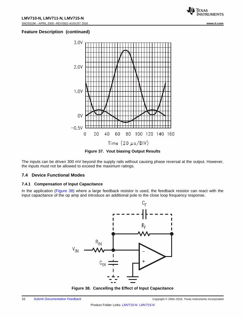
To achieve maximum output swing, the output must be biased at mid-supply. This is normally done by biasingthe input at mid-supply. But with supply voltage range from 2 V to 3.4 V, the input of the op amp must not bebiased at mid-supply because of the transition of the VOS. Figure 36 shows an example of how to get away fromthe VOS crossover point and maintain a maximum swing with a 2.7-V supply. Figure 37 shows the waveforms ofVIN and VOUT.
Figure 36. Vout biasing Example
16
LMV710-N, LMV711-N, LMV715-NSNOS519K –APRIL 2000–REVISED AUGUST 2016 www.ti.com
Product Folder Links: LMV710-N LMV715-N
Submit Documentation Feedback Copyright © 2000–2016, Texas Instruments Incorporated
Feature Description (continued)
Figure 37. Vout biasing Output Results
The inputs can be driven 300 mV beyond the supply rails without causing phase reversal at the output. However,the inputs must not be allowed to exceed the maximum ratings.
7.4 Device Functional Modes
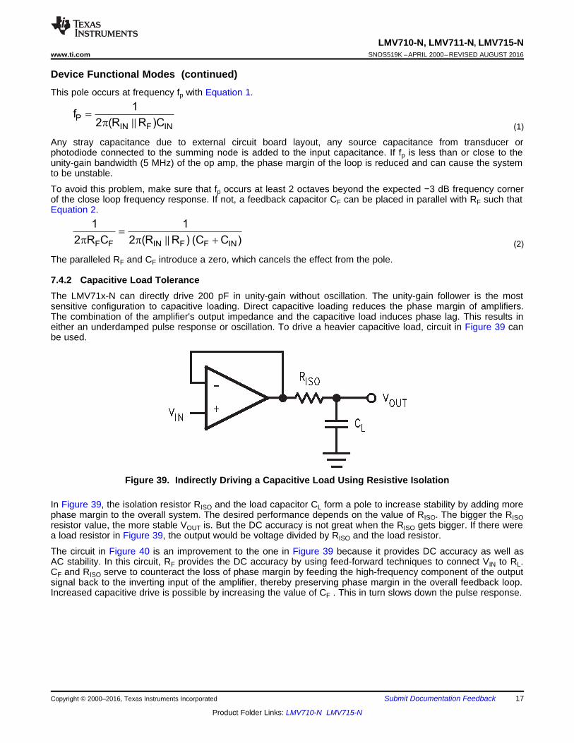
7.4.1 Compensation of Input CapacitanceIn the application (Figure 38) where a large feedback resistor is used, the feedback resistor can react with theinput capacitance of the op amp and introduce an additional pole to the close loop frequency response.
Figure 38. Cancelling the Effect of Input Capacitance
=
p p +PF F IN F F IN
1 1
2 R C 2 (R R ) (C C )
=
p PP
IN F IN
1f
2 (R R )C
17
LMV710-N, LMV711-N, LMV715-Nwww.ti.com SNOS519K –APRIL 2000–REVISED AUGUST 2016
Product Folder Links: LMV710-N LMV715-N
Submit Documentation FeedbackCopyright © 2000–2016, Texas Instruments Incorporated
Device Functional Modes (continued)This pole occurs at frequency fp with Equation 1.
(1)
Any stray capacitance due to external circuit board layout, any source capacitance from transducer orphotodiode connected to the summing node is added to the input capacitance. If fp is less than or close to theunity-gain bandwidth (5 MHz) of the op amp, the phase margin of the loop is reduced and can cause the systemto be unstable.
To avoid this problem, make sure that fp occurs at least 2 octaves beyond the expected −3 dB frequency cornerof the close loop frequency response. If not, a feedback capacitor CF can be placed in parallel with RF such thatEquation 2.
(2)
The paralleled RF and CF introduce a zero, which cancels the effect from the pole.
7.4.2 Capacitive Load ToleranceThe LMV71x-N can directly drive 200 pF in unity-gain without oscillation. The unity-gain follower is the mostsensitive configuration to capacitive loading. Direct capacitive loading reduces the phase margin of amplifiers.The combination of the amplifier's output impedance and the capacitive load induces phase lag. This results ineither an underdamped pulse response or oscillation. To drive a heavier capacitive load, circuit in Figure 39 canbe used.
Figure 39. Indirectly Driving a Capacitive Load Using Resistive Isolation
In Figure 39, the isolation resistor RISO and the load capacitor CL form a pole to increase stability by adding morephase margin to the overall system. The desired performance depends on the value of RISO. The bigger the RISOresistor value, the more stable VOUT is. But the DC accuracy is not great when the RISO gets bigger. If there werea load resistor in Figure 39, the output would be voltage divided by RISO and the load resistor.
The circuit in Figure 40 is an improvement to the one in Figure 39 because it provides DC accuracy as well asAC stability. In this circuit, RF provides the DC accuracy by using feed-forward techniques to connect VIN to RL.CF and RISO serve to counteract the loss of phase margin by feeding the high-frequency component of the outputsignal back to the inverting input of the amplifier, thereby preserving phase margin in the overall feedback loop.Increased capacitive drive is possible by increasing the value of CF . This in turn slows down the pulse response.

18
LMV710-N, LMV711-N, LMV715-NSNOS519K –APRIL 2000–REVISED AUGUST 2016 www.ti.com
Product Folder Links: LMV710-N LMV715-N
Submit Documentation Feedback Copyright © 2000–2016, Texas Instruments Incorporated
Device Functional Modes (continued)
Figure 40. Indirectly Driving a Capacitive a Load With DC Accuracy

Copyright © 2016, Texas Instruments Incorporated
±
+
ICHARGE
±
+
RSENSE 0.2
2 k
2 k
R2
R1
Load10 kR3
VOUT
Q12N3906
V+
SENSE 3OUT Charge Charge
1
R RV I 1 I
R
x x : x
19
LMV710-N, LMV711-N, LMV715-Nwww.ti.com SNOS519K –APRIL 2000–REVISED AUGUST 2016
Product Folder Links: LMV710-N LMV715-N
Submit Documentation FeedbackCopyright © 2000–2016, Texas Instruments Incorporated
8 Application and Implementation
NOTEInformation in the following applications sections is not part of the TI componentspecification, and TI does not warrant its accuracy or completeness. TI’s customers areresponsible for determining suitability of components for their purposes. Customers shouldvalidate and test their design implementation to confirm system functionality.
8.1 Application InformationThe LMV71x family of amplifiers features low voltage, low power, and rail-to-rail output operational amplifiersdesigned for low-voltage portable applications.
8.2 Typical Applications
8.2.1 High-Side Current-Sensing
Figure 41. High-Side, Current-Sensing Schematic
8.2.1.1 Design RequirementsThe high-side, current-sensing circuit (Figure 41) is commonly used in a battery charger to monitor chargingcurrent to prevent over charging. A sense resistor RSENSE is connected to the battery directly. This systemrequires an op amp with rail-to-rail input. The LMV71x are ideal for this application because its common-modeinput range goes up to the rail.
8.2.1.2 Detailed Design ProcedureAs seen in (Figure 41), the ICHARGE current flowing through sense resistor RSENSE develops a voltage drop equalto VSENSE. The voltage at the negative sense point is now less than the positive sense point by an amountproportional to the VSENSE voltage.
The low-bias currents of the LMV71x cause little voltage drop through R2, so the negative input of the LMV71xamplifier is at essentially the same potential as the negative sense input.
The LMV71x detects this voltage error between its inputs and servo the transistor base to conduct more currentthrough Q1, increasing the voltage drop across R1 until the LMV71x inverting input matches the noninvertinginput. At this point, the voltage drop across R1 now matches VSENSE.
IG, a current proportional to ICHARGE, flows according to Equation 3.

Copyright © 2016, Texas Instruments Incorporated
VIN
R1
10 k
Reset 2N2945
R5 C110 k
R3D1
R2
10 k
V+
1N914A
LMV71x(A2)
LMV71x(A1)
R4
10 k
V+
VO
+
-
+
-
1
2
3
4
5
1 2 3 4 5
VO
UT
(V
)
ILOAD (A)
VOUT (V)
C003
20
LMV710-N, LMV711-N, LMV715-NSNOS519K –APRIL 2000–REVISED AUGUST 2016 www.ti.com
Product Folder Links: LMV710-N LMV715-N
Submit Documentation Feedback Copyright © 2000–2016, Texas Instruments Incorporated
Typical Applications (continued)IG = VRSENSE / R1 = ( RSENSE × ICHARGE ) / R1 (3)
IG also flows through the gain resistor R3 developing a voltage drop equal to Equation 4.V3 = IG × R3 = ( VRSENSE / R1 ) × R3 = ( ( RSENSE × ICHARGE ) / R2 ) × R3 (4)VOUT = (RSENSE × ICHARGE ) × G
where• G = R3 / R1 (5)
The other channel of the LMV71x may be used to buffer the voltage across R3 to drive the following stages.
8.2.1.3 Application Curve
Figure 42. High-Side Current-Sensing Results
8.2.2 Peak Detector
Figure 43. Peak Detector
8.2.2.1 Design RequirementsA peak detector outputs a DC voltage equal to the peak value of the applied AC signal. Peak detectors are usedin many applications, such as test equipment, measurement instrumentation, ultrasonic alarm systems, and soforth. Figure 43 shows the schematic diagram of a peak detector using LMV71x-N. This peak detector basicallyconsists of a clipper, a parallel RC network, and a voltage follower.

RF Signal IN OUT
U1 GSM PA
VPC
Directional Coupler
C2
U2
Input
Coupled Load
Output
C4 BIAS
VCC
GSMANTENNA
R5
RLOAD
R2
R3
C5+
±
OUT
C3
R1
VCC
U3
V-
R4
SD
Shut Down RampUp/Down
V+
Schottky Diode Detector
Copyright © 2016, Texas Instruments Incorporated
21
LMV710-N, LMV711-N, LMV715-Nwww.ti.com SNOS519K –APRIL 2000–REVISED AUGUST 2016
Product Folder Links: LMV710-N LMV715-N
Submit Documentation FeedbackCopyright © 2000–2016, Texas Instruments Incorporated
Typical Applications (continued)8.2.2.2 Detailed Design ProcedureAn AC voltage source applied to VIN charges capacitor C1 to the peak of the input. Diode D1 conducts positivehalf cycles, charging C1 to the waveform peak. Including D1 inside the feedback loop of the amplifier removesthe voltage drop of D1 and allows an accurate peak detection of VIN on C1. When the input waveform falls belowthe DC peak stored on C1, D1 is reverse biased. The low input bias current of A1 and the reverse biasing of D1limits current leakage from C1. As a result, C1 retains the peak value even as the waveform drops to zero. A2further isolates the peak value on C1 while completing the peak detector circuit by operating as a voltagefollower and reporting the peak voltage of C1 at its output.
R5 and C1 are properly selected so that the capacitor is charged rapidly to VIN. During the holding period, thecapacitor slowly discharge through C1, through leakage of the capacitor and the reverse-biased diode, or op ampbias currents. In any cases the discharging time constant is much larger than the charge time constant. And thecapacitor can hold its voltage long enough to minimize the output ripple.
Resistors R2 and R3 limit the current into the inverting input of A1 and the noninverting input of A2 when poweris disconnected from the circuit. The discharging current from C1 during power off may damage the input circuitryof the op amps.
The peak detector is reset by applying a positive pulse to the reset transistor. The charge on the capacitor isdumped into ground, and the detector is ready for another cycle.
The maximum input voltage to this detector must be less than (V+ – VD), where VD is the forward voltage drop ofthe diode. Otherwise, the input voltage must be scaled down before applying to the circuit.
8.2.3 GSM Power Amplifier Control Loop
Figure 44. GSM P.A. Control Loop
8.2.3.1 Design RequirementsThe control loop in Figure 44 controls the output power level of a GSM mobile phones. The control loop is usedto avoid intermodulation of Base Station receivers, to prevent intermodulation with other mobile phones, and tominimize power consumption depending on the distance between mobile and base station

Rin
OUTPUT
Rf
Cf
Cbyp
SHDN
GND
V+
INPUT
GND
22
LMV710-N, LMV711-N, LMV715-NSNOS519K –APRIL 2000–REVISED AUGUST 2016 www.ti.com
Product Folder Links: LMV710-N LMV715-N
Submit Documentation Feedback Copyright © 2000–2016, Texas Instruments Incorporated
Typical Applications (continued)8.2.3.2 Detailed Design ProcedureThere are four critical sections in the GSM Power Amplifier Control Loop. The class-C RF power amplifierprovides amplification of the RF signal. A directional coupler couples small amount of RF energy from the outputof the RF P. A. to an envelope detector diode. The detector diode senses the signal level and rectifies it to a DClevel to indicate the signal strength at the antenna. An op amp is used as an error amplifier to process the diodevoltage and ramping voltage. This loop control the power amplifier gain through the op amp and forces thedetector diode voltage and ramping voltage to be equal. Power control is accomplished by changing the rampingvoltage.
The LMV71x-N are well suited as an error amplifier in this application. The LMV711 or LMV715 have an extrashutdown pin to switch the op amp to shutdown mode. In shutdown mode, the LMV711 or LMV715 consumevery low current. The LMV711 provides a ground voltage to the power amplifier control pin VPC. Therefore, thepower amplifier can be turned off to save battery life. The LMV715 output is tri-stated when in shutdown.
9 Power Supply RecommendationsFor proper operation, the power supplies must be properly decoupled. For decoupling the supply lines, TIrecommends that 10-nF capacitors be placed as close as possible to the power supply pins of the operationalamplifier. For single supply, place a capacitor between V+ and V– supply leads. For dual supplies, place onecapacitor between V+ and ground, and one capacitor between V– and ground.
10 Layout
10.1 Layout GuidelinesTo properly bypass the power supply, several locations on a printed-circuit board must be considered. A 6.8-µFor greater tantalum capacitor must be placed at the point where the power supply for the amplifier is introducedonto the board. Another 0.1-µF ceramic capacitor must be placed as close as possible to the power supply pin ofthe amplifier. If the amplifier is operated in a single power supply, only the V+ pin requires a bypass with a 0.1-µFcapacitor. If the amplifier is operated in a dual power supply, both V+ and V– pins must be bypassed. It is goodpractice to use a ground plane on a printed-circuit board to provide all components with a low inductive groundconnection.
10.2 Layout Example
Figure 45. LMV711 Layout Example

23
LMV710-N, LMV711-N, LMV715-Nwww.ti.com SNOS519K –APRIL 2000–REVISED AUGUST 2016
Product Folder Links: LMV710-N LMV715-N
Submit Documentation FeedbackCopyright © 2000–2016, Texas Instruments Incorporated
11 Device and Documentation Support
11.1 Device Support
11.1.1 Development SupportFor development support see the following:• LMV710 PSPICE Model (applicable for LMV711 and LMV715)• SPICE-based analog simulation program, TINA-TI• DIP adapter evaluation module, DIP Adapter EVM• TI universal operational amplifier evaluation module, Op Amp EVM• TI software, FilterPro
11.2 Documentation Support
11.2.1 Related DocumentationFor related documentation see the following:• Absolute Maximum Ratings for Soldering (SNOA549)• AN-29 IC Op Amp Beats FETs on Input Current (SNOA624)• AN-31 Op Amp Circuit Collection (SNLA140)• AN-71 Micropower Circuits Using the LM4250 Programmable Op Amp (SNOA652)• AN-127 LM143 Monolithic High Voltage Operational Amplifier Applications (SNVA516)
11.3 Related LinksThe table below lists quick access links. Categories include technical documents, support and communityresources, tools and software, and quick access to sample or buy.
Table 1. Related Links
PARTS PRODUCT FOLDER SAMPLE & BUY TECHNICALDOCUMENTS
TOOLS &SOFTWARE
SUPPORT &COMMUNITY
LMV710-N Click here Click here Click here Click here Click hereLMV711-N Click here Click here Click here Click here Click hereLMV715-N Click here Click here Click here Click here Click here
11.4 Receiving Notification of Documentation UpdatesTo receive notification of documentation updates, navigate to the device product folder on ti.com. In the upperright corner, click on Alert me to register and receive a weekly digest of any product information that haschanged. For change details, review the revision history included in any revised document.
11.5 Community ResourcesThe following links connect to TI community resources. Linked contents are provided "AS IS" by the respectivecontributors. They do not constitute TI specifications and do not necessarily reflect TI's views; see TI's Terms ofUse.
TI E2E™ Online Community TI's Engineer-to-Engineer (E2E) Community. Created to foster collaborationamong engineers. At e2e.ti.com, you can ask questions, share knowledge, explore ideas and helpsolve problems with fellow engineers.
Design Support TI's Design Support Quickly find helpful E2E forums along with design support tools andcontact information for technical support.
11.6 TrademarksE2E is a trademark of Texas Instruments.All other trademarks are the property of their respective owners.
24
LMV710-N, LMV711-N, LMV715-NSNOS519K –APRIL 2000–REVISED AUGUST 2016 www.ti.com
Product Folder Links: LMV710-N LMV715-N
Submit Documentation Feedback Copyright © 2000–2016, Texas Instruments Incorporated
11.7 Electrostatic Discharge CautionThese devices have limited built-in ESD protection. The leads should be shorted together or the device placed in conductive foamduring storage or handling to prevent electrostatic damage to the MOS gates.
11.8 GlossarySLYZ022 — TI Glossary.
This glossary lists and explains terms, acronyms, and definitions.
12 Mechanical, Packaging, and Orderable InformationThe following pages include mechanical, packaging, and orderable information. This information is the mostcurrent data available for the designated devices. This data is subject to change without notice and revision ofthis document. For browser-based versions of this data sheet, refer to the left-hand navigation.

PACKAGE OPTION ADDENDUM
www.ti.com 26-Sep-2017
Addendum-Page 1
PACKAGING INFORMATION
Orderable Device Status(1)
Package Type PackageDrawing
Pins PackageQty
Eco Plan(2)
Lead/Ball Finish(6)
MSL Peak Temp(3)
Op Temp (°C) Device Marking(4/5)
Samples
LMV710M5 NRND SOT-23 DBV 5 1000 TBD Call TI Call TI -40 to 85 A48A
LMV710M5/NOPB ACTIVE SOT-23 DBV 5 1000 Green (RoHS& no Sb/Br)
CU SN Level-1-260C-UNLIM -40 to 85 A48A
LMV710M5X/NOPB ACTIVE SOT-23 DBV 5 3000 Green (RoHS& no Sb/Br)
CU SN Level-1-260C-UNLIM -40 to 85 A48A
(1) The marketing status values are defined as follows:ACTIVE: Product device recommended for new designs.LIFEBUY: TI has announced that the device will be discontinued, and a lifetime-buy period is in effect.NRND: Not recommended for new designs. Device is in production to support existing customers, but TI does not recommend using this part in a new design.PREVIEW: Device has been announced but is not in production. Samples may or may not be available.OBSOLETE: TI has discontinued the production of the device.
(2) RoHS: TI defines "RoHS" to mean semiconductor products that are compliant with the current EU RoHS requirements for all 10 RoHS substances, including the requirement that RoHS substancedo not exceed 0.1% by weight in homogeneous materials. Where designed to be soldered at high temperatures, "RoHS" products are suitable for use in specified lead-free processes. TI mayreference these types of products as "Pb-Free".RoHS Exempt: TI defines "RoHS Exempt" to mean products that contain lead but are compliant with EU RoHS pursuant to a specific EU RoHS exemption.Green: TI defines "Green" to mean the content of Chlorine (Cl) and Bromine (Br) based flame retardants meet JS709B low halogen requirements of <=1000ppm threshold. Antimony trioxide basedflame retardants must also meet the <=1000ppm threshold requirement.
(3) MSL, Peak Temp. - The Moisture Sensitivity Level rating according to the JEDEC industry standard classifications, and peak solder temperature.
(4) There may be additional marking, which relates to the logo, the lot trace code information, or the environmental category on the device.
(5) Multiple Device Markings will be inside parentheses. Only one Device Marking contained in parentheses and separated by a "~" will appear on a device. If a line is indented then it is a continuationof the previous line and the two combined represent the entire Device Marking for that device.
(6) Lead/Ball Finish - Orderable Devices may have multiple material finish options. Finish options are separated by a vertical ruled line. Lead/Ball Finish values may wrap to two lines if the finishvalue exceeds the maximum column width.
Important Information and Disclaimer:The information provided on this page represents TI's knowledge and belief as of the date that it is provided. TI bases its knowledge and belief on informationprovided by third parties, and makes no representation or warranty as to the accuracy of such information. Efforts are underway to better integrate information from third parties. TI has taken andcontinues to take reasonable steps to provide representative and accurate information but may not have conducted destructive testing or chemical analysis on incoming materials and chemicals.TI and TI suppliers consider certain information to be proprietary, and thus CAS numbers and other limited information may not be available for release.
In no event shall TI's liability arising out of such information exceed the total purchase price of the TI part(s) at issue in this document sold by TI to Customer on an annual basis.

PACKAGE OPTION ADDENDUM
www.ti.com 26-Sep-2017
Addendum-Page 2

TAPE AND REEL INFORMATION
*All dimensions are nominal
Device PackageType
PackageDrawing
Pins SPQ ReelDiameter
(mm)
ReelWidth
W1 (mm)
A0(mm)
B0(mm)
K0(mm)
P1(mm)
W(mm)
Pin1Quadrant
LMV710M5 SOT-23 DBV 5 1000 178.0 8.4 3.2 3.2 1.4 4.0 8.0 Q3
LMV710M5/NOPB SOT-23 DBV 5 1000 178.0 8.4 3.2 3.2 1.4 4.0 8.0 Q3
LMV710M5X/NOPB SOT-23 DBV 5 3000 178.0 8.4 3.2 3.2 1.4 4.0 8.0 Q3
PACKAGE MATERIALS INFORMATION
www.ti.com 24-Aug-2017
Pack Materials-Page 1

*All dimensions are nominal
Device Package Type Package Drawing Pins SPQ Length (mm) Width (mm) Height (mm)
LMV710M5 SOT-23 DBV 5 1000 210.0 185.0 35.0
LMV710M5/NOPB SOT-23 DBV 5 1000 210.0 185.0 35.0
LMV710M5X/NOPB SOT-23 DBV 5 3000 210.0 185.0 35.0
PACKAGE MATERIALS INFORMATION
www.ti.com 24-Aug-2017
Pack Materials-Page 2


www.ti.com
PACKAGE OUTLINE
C
TYP0.220.08
0.25
3.02.6
2X 0.95
1.9
1.45 MAX
TYP0.150.00
5X 0.50.3
TYP0.60.3
TYP80
1.9
A
3.052.75
B1.751.45
(1.1)
SOT-23 - 1.45 mm max heightDBV0005ASMALL OUTLINE TRANSISTOR
4214839/C 04/2017
NOTES: 1. All linear dimensions are in millimeters. Any dimensions in parenthesis are for reference only. Dimensioning and tolerancing per ASME Y14.5M.2. This drawing is subject to change without notice.3. Refernce JEDEC MO-178.
0.2 C A B
1
34
5
2
INDEX AREAPIN 1
GAGE PLANE
SEATING PLANE
0.1 C
SCALE 4.000

www.ti.com
EXAMPLE BOARD LAYOUT
0.07 MAXARROUND
0.07 MINARROUND
5X (1.1)
5X (0.6)
(2.6)
(1.9)
2X (0.95)
(R0.05) TYP
4214839/C 04/2017
SOT-23 - 1.45 mm max heightDBV0005ASMALL OUTLINE TRANSISTOR
NOTES: (continued) 4. Publication IPC-7351 may have alternate designs. 5. Solder mask tolerances between and around signal pads can vary based on board fabrication site.
SYMM
LAND PATTERN EXAMPLEEXPOSED METAL SHOWN
SCALE:15X
PKG
1
3 4
5
2
SOLDER MASKOPENINGMETAL UNDER
SOLDER MASK
SOLDER MASKDEFINED
EXPOSED METAL
METALSOLDER MASKOPENING
NON SOLDER MASKDEFINED
(PREFERRED)
SOLDER MASK DETAILS
EXPOSED METAL

www.ti.com
EXAMPLE STENCIL DESIGN
(2.6)
(1.9)
2X(0.95)
5X (1.1)
5X (0.6)
(R0.05) TYP
SOT-23 - 1.45 mm max heightDBV0005ASMALL OUTLINE TRANSISTOR
4214839/C 04/2017
NOTES: (continued) 6. Laser cutting apertures with trapezoidal walls and rounded corners may offer better paste release. IPC-7525 may have alternate design recommendations. 7. Board assembly site may have different recommendations for stencil design.
SOLDER PASTE EXAMPLEBASED ON 0.125 mm THICK STENCIL
SCALE:15X
SYMM
PKG
1
3 4
5
2

IMPORTANT NOTICE
Texas Instruments Incorporated (TI) reserves the right to make corrections, enhancements, improvements and other changes to itssemiconductor products and services per JESD46, latest issue, and to discontinue any product or service per JESD48, latest issue. Buyersshould obtain the latest relevant information before placing orders and should verify that such information is current and complete.TI’s published terms of sale for semiconductor products (http://www.ti.com/sc/docs/stdterms.htm) apply to the sale of packaged integratedcircuit products that TI has qualified and released to market. Additional terms may apply to the use or sale of other types of TI products andservices.Reproduction of significant portions of TI information in TI data sheets is permissible only if reproduction is without alteration and isaccompanied by all associated warranties, conditions, limitations, and notices. TI is not responsible or liable for such reproduceddocumentation. Information of third parties may be subject to additional restrictions. Resale of TI products or services with statementsdifferent from or beyond the parameters stated by TI for that product or service voids all express and any implied warranties for theassociated TI product or service and is an unfair and deceptive business practice. TI is not responsible or liable for any such statements.Buyers and others who are developing systems that incorporate TI products (collectively, “Designers”) understand and agree that Designersremain responsible for using their independent analysis, evaluation and judgment in designing their applications and that Designers havefull and exclusive responsibility to assure the safety of Designers' applications and compliance of their applications (and of all TI productsused in or for Designers’ applications) with all applicable regulations, laws and other applicable requirements. Designer represents that, withrespect to their applications, Designer has all the necessary expertise to create and implement safeguards that (1) anticipate dangerousconsequences of failures, (2) monitor failures and their consequences, and (3) lessen the likelihood of failures that might cause harm andtake appropriate actions. Designer agrees that prior to using or distributing any applications that include TI products, Designer willthoroughly test such applications and the functionality of such TI products as used in such applications.TI’s provision of technical, application or other design advice, quality characterization, reliability data or other services or information,including, but not limited to, reference designs and materials relating to evaluation modules, (collectively, “TI Resources”) are intended toassist designers who are developing applications that incorporate TI products; by downloading, accessing or using TI Resources in anyway, Designer (individually or, if Designer is acting on behalf of a company, Designer’s company) agrees to use any particular TI Resourcesolely for this purpose and subject to the terms of this Notice.TI’s provision of TI Resources does not expand or otherwise alter TI’s applicable published warranties or warranty disclaimers for TIproducts, and no additional obligations or liabilities arise from TI providing such TI Resources. TI reserves the right to make corrections,enhancements, improvements and other changes to its TI Resources. TI has not conducted any testing other than that specificallydescribed in the published documentation for a particular TI Resource.Designer is authorized to use, copy and modify any individual TI Resource only in connection with the development of applications thatinclude the TI product(s) identified in such TI Resource. NO OTHER LICENSE, EXPRESS OR IMPLIED, BY ESTOPPEL OR OTHERWISETO ANY OTHER TI INTELLECTUAL PROPERTY RIGHT, AND NO LICENSE TO ANY TECHNOLOGY OR INTELLECTUAL PROPERTYRIGHT OF TI OR ANY THIRD PARTY IS GRANTED HEREIN, including but not limited to any patent right, copyright, mask work right, orother intellectual property right relating to any combination, machine, or process in which TI products or services are used. Informationregarding or referencing third-party products or services does not constitute a license to use such products or services, or a warranty orendorsement thereof. Use of TI Resources may require a license from a third party under the patents or other intellectual property of thethird party, or a license from TI under the patents or other intellectual property of TI.TI RESOURCES ARE PROVIDED “AS IS” AND WITH ALL FAULTS. TI DISCLAIMS ALL OTHER WARRANTIES ORREPRESENTATIONS, EXPRESS OR IMPLIED, REGARDING RESOURCES OR USE THEREOF, INCLUDING BUT NOT LIMITED TOACCURACY OR COMPLETENESS, TITLE, ANY EPIDEMIC FAILURE WARRANTY AND ANY IMPLIED WARRANTIES OFMERCHANTABILITY, FITNESS FOR A PARTICULAR PURPOSE, AND NON-INFRINGEMENT OF ANY THIRD PARTY INTELLECTUALPROPERTY RIGHTS. TI SHALL NOT BE LIABLE FOR AND SHALL NOT DEFEND OR INDEMNIFY DESIGNER AGAINST ANY CLAIM,INCLUDING BUT NOT LIMITED TO ANY INFRINGEMENT CLAIM THAT RELATES TO OR IS BASED ON ANY COMBINATION OFPRODUCTS EVEN IF DESCRIBED IN TI RESOURCES OR OTHERWISE. IN NO EVENT SHALL TI BE LIABLE FOR ANY ACTUAL,DIRECT, SPECIAL, COLLATERAL, INDIRECT, PUNITIVE, INCIDENTAL, CONSEQUENTIAL OR EXEMPLARY DAMAGES INCONNECTION WITH OR ARISING OUT OF TI RESOURCES OR USE THEREOF, AND REGARDLESS OF WHETHER TI HAS BEENADVISED OF THE POSSIBILITY OF SUCH DAMAGES.Unless TI has explicitly designated an individual product as meeting the requirements of a particular industry standard (e.g., ISO/TS 16949and ISO 26262), TI is not responsible for any failure to meet such industry standard requirements.Where TI specifically promotes products as facilitating functional safety or as compliant with industry functional safety standards, suchproducts are intended to help enable customers to design and create their own applications that meet applicable functional safety standardsand requirements. Using products in an application does not by itself establish any safety features in the application. Designers mustensure compliance with safety-related requirements and standards applicable to their applications. Designer may not use any TI products inlife-critical medical equipment unless authorized officers of the parties have executed a special contract specifically governing such use.Life-critical medical equipment is medical equipment where failure of such equipment would cause serious bodily injury or death (e.g., lifesupport, pacemakers, defibrillators, heart pumps, neurostimulators, and implantables). Such equipment includes, without limitation, allmedical devices identified by the U.S. Food and Drug Administration as Class III devices and equivalent classifications outside the U.S.TI may expressly designate certain products as completing a particular qualification (e.g., Q100, Military Grade, or Enhanced Product).Designers agree that it has the necessary expertise to select the product with the appropriate qualification designation for their applicationsand that proper product selection is at Designers’ own risk. Designers are solely responsible for compliance with all legal and regulatoryrequirements in connection with such selection.Designer will fully indemnify TI and its representatives against any damages, costs, losses, and/or liabilities arising out of Designer’s non-compliance with the terms and provisions of this Notice.
Mailing Address: Texas Instruments, Post Office Box 655303, Dallas, Texas 75265Copyright © 2018, Texas Instruments Incorporated