Embed Size (px)
Citation preview
ADD OUTN
VDDOE
GND OUTP
SCL
SDA
1 6
2 5
43
7
8
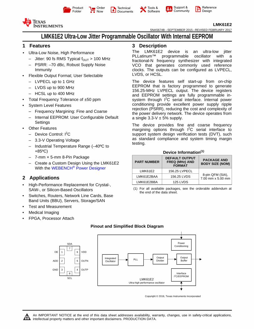
LMK61E2Ultra-high performance oscillator
PLLOutput Divider
Output Buffer
Power Conditioning
InterfaceI2C/EEPROM
Integrated Oscillator
Copyright © 2016, Texas Instruments Incorporated
Product
Folder
Order
Now
Technical
Documents
Tools &
Software
Support &Community
ReferenceDesign
An IMPORTANT NOTICE at the end of this data sheet addresses availability, warranty, changes, use in safety-critical applications,intellectual property matters and other important disclaimers. PRODUCTION DATA.
LMK61E2SNAS674B –SEPTEMBER 2015–REVISED FEBRUARY 2017
LMK61E2 Ultra-Low Jitter Programmable Oscillator With Internal EEPROM
1
1 Features1• Ultra-Low Noise, High Performance
– Jitter: 90 fs RMS Typical fOUT > 100 MHz– PSRR: –70 dBc, Robust Supply Noise
Immunity• Flexible Output Format; User Selectable
– LVPECL up to 1 GHz– LVDS up to 900 MHz– HCSL up to 400 MHz
• Total Frequency Tolerance of ±50 ppm• System Level Features
– Frequency Margining: Fine and Coarse– Internal EEPROM: User Configurable Default
Settings• Other Features
– Device Control: I2C– 3.3-V Operating Voltage– Industrial Temperature Range (–40ºC to
+85ºC)– 7-mm × 5-mm 8-Pin Package– Create a Custom Design Using the LMK61E2
With the WEBENCH® Power Designer
2 Applications• High-Performance Replacement for Crystal-,
SAW-, or Silicon-Based Oscillators• Switches, Routers, Network Line Cards, Base
Band Units (BBU), Servers, Storage/SAN• Test and Measurement• Medical Imaging• FPGA, Processor Attach
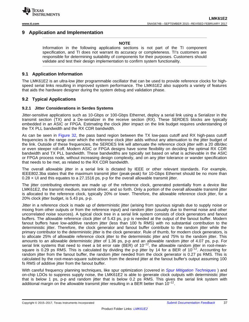
3 DescriptionThe LMK61E2 device is an ultra-low jitterPLLatinum™ programmable oscillator with afractional-N frequency synthesizer with integratedVCO that generates commonly used referenceclocks. The outputs can be configured as LVPECL,LVDS, or HCSL.
The device features self start-up from on-chipEEPROM that is factory programmed to generate156.25-MHz LVPECL output. The device registersand EEPROM settings are fully programmable in-system through I2C serial interface. Internal powerconditioning provide excellent power supply ripplerejection (PSRR), reducing the cost and complexity ofthe power delivery network. The device operates froma single 3.3-V ± 5% supply.
The device provides fine and coarse frequencymargining options through I2C serial interface tosupport system design verification tests (DVT), suchas standard compliance and system timing margintesting.
Device Information(1)
PART NUMBERDEFAULT OUTPUTFREQ (MHz) AND
FORMATPACKAGE AND
BODY SIZE (NOM)
LMK61E2 156.25 LVPECL8-pin QFM (SIA),
7.00 mm x 5.00 mmLMK61E2BAA 156.25 LVDSLMK61E2BBA 125 LVDS
(1) For all available packages, see the orderable addendum atthe end of the data sheet.
Pinout and Simplified Block Diagram
2
LMK61E2SNAS674B –SEPTEMBER 2015–REVISED FEBRUARY 2017 www.ti.com
Product Folder Links: LMK61E2
Submit Documentation Feedback Copyright © 2015–2017, Texas Instruments Incorporated
Table of Contents1 Features .................................................................. 12 Applications ........................................................... 13 Description ............................................................. 14 Revision History..................................................... 25 Pin Configuration and Functions ......................... 36 Specifications......................................................... 3
6.1 Absolute Maximum Ratings ...................................... 36.2 ESD Ratings ............................................................ 36.3 Recommended Operating Conditions....................... 46.4 Thermal Information .................................................. 46.5 Electrical Characteristics - Power Supply ................. 46.6 LVPECL Output Characteristics................................ 56.7 LVDS Output Characteristics .................................... 56.8 HCSL Output Characteristics.................................... 56.9 OE Input Characteristics ........................................... 66.10 ADD Input Characteristics....................................... 66.11 Frequency Tolerance Characteristics ..................... 66.12 Power-On/Reset Characteristics (VDD).................. 66.13 I2C-Compatible Interface Characteristics (SDA,
SCL) ........................................................................... 66.14 PSRR Characteristics ............................................. 76.15 Other Characteristics .............................................. 76.16 PLL Clock Output Jitter Characteristics .................. 76.17 Typical 156.25-MHz Output Phase Noise
Characteristics ........................................................... 86.18 Typical 161.1328125 MHz Output Phase Noise
Characteristics ........................................................... 86.19 Additional Reliability and Qualification .................... 8
6.20 Typical Characteristics ............................................ 97 Parameter Measurement Information ................ 12
7.1 Device Output Configurations ................................. 128 Detailed Description ............................................ 14
8.1 Overview ................................................................. 148.2 Functional Block Diagram ....................................... 148.3 Feature Description................................................. 148.4 Device Functional Modes........................................ 188.5 Programming........................................................... 198.6 EEPROM Map......................................................... 238.7 Register Map........................................................... 25
9 Application and Implementation ........................ 379.1 Application Information............................................ 379.2 Typical Applications ................................................ 37
10 Power Supply Recommendations ..................... 4311 Layout................................................................... 44
11.1 Layout Guidelines ................................................. 4411.2 Layout Example .................................................... 45
12 Device and Documentation Support ................. 4612.1 Device Support...................................................... 4612.2 Documentation Support ........................................ 4612.3 Receiving Notification of Documentation Updates 4612.4 Community Resources.......................................... 4612.5 Trademarks ........................................................... 4612.6 Electrostatic Discharge Caution............................ 4712.7 Glossary ................................................................ 47
13 Mechanical, Packaging, and OrderableInformation ........................................................... 47
4 Revision History
Changes from Revision A (September 2015) to Revision B Page
• Added WEBENCH links and information for custom designs ............................................................................................... 1• New release of LMK61E2BAA, LMK61E2BBA....................................................................................................................... 1• Updated data sheet text to latest documentation and translations standards ...................................................................... 1• Moved Figure 34 to Layout Example.................................................................................................................................... 45
Changes from Original (September 2015) to Revision A Page
• Moved conditions from figure title to table under each graphic.............................................................................................. 9• Updated Figure 26 ............................................................................................................................................................... 18• Added Related Documentation section. ............................................................................................................................... 46
ADD OUTN
VDDOE
GND OUTP
SCL
SDA
1 6
2 5
43
7
8
3
LMK61E2www.ti.com SNAS674B –SEPTEMBER 2015–REVISED FEBRUARY 2017
Product Folder Links: LMK61E2
Submit Documentation FeedbackCopyright © 2015–2017, Texas Instruments Incorporated
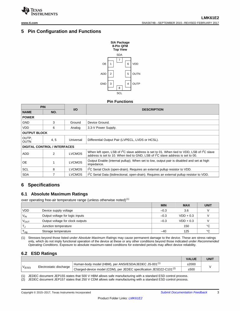
5 Pin Configuration and Functions
SIA Package8-Pin QFMTop View
Pin FunctionsPIN
I/O DESCRIPTIONNAME NO.POWERGND 3 Ground Device Ground.VDD 6 Analog 3.3-V Power Supply.OUTPUT BLOCKOUTP,OUTN 4, 5 Universal Differential Output Pair (LVPECL, LVDS or HCSL).
DIGITAL CONTROL / INTERFACES
ADD 2 LVCMOS When left open, LSB of I2C slave address is set to 01. When tied to VDD, LSB of I2C slaveaddress is set to 10. When tied to GND, LSB of I2C slave address is set to 00.
OE 1 LVCMOS Output Enable (internal pullup). When set to low, output pair is disabled and set at highimpedance.
SCL 8 LVCMOS I2C Serial Clock (open-drain). Requires an external pullup resistor to VDD.SDA 7 LVCMOS I2C Serial Data (bidirectional, open-drain). Requires an external pullup resistor to VDD.
(1) Stresses beyond those listed under Absolute Maximum Ratings may cause permanent damage to the device. These are stress ratingsonly, which do not imply functional operation of the device at these or any other conditions beyond those indicated under RecommendedOperating Conditions. Exposure to absolute maximum-rated conditions for extended periods may affect device reliability.
6 Specifications
6.1 Absolute Maximum Ratingsover operating free-air temperature range (unless otherwise noted) (1)
MIN MAX UNITVDD Device supply voltage –0.3 3.6 VVIN Output voltage for logic inputs –0.3 VDD + 0.3 VVOUT Output voltage for clock outputs –0.3 VDD + 0.3 VTJ Junction temperature 150 °CTstg Storage temperature –40 125 °C
(1) JEDEC document JEP155 states that 500 V HBM allows safe manufacturing with a standard ESD control process.(2) JEDEC document JEP157 states that 250 V CDM allows safe manufacturing with a standard ESD control process.
6.2 ESD RatingsVALUE UNIT
V(ESD) Electrostatic dischargeHuman-body model (HBM), per ANSI/ESDA/JEDEC JS-001 (1) ±2000
VCharged-device model (CDM), per JEDEC specification JESD22-C101 (2) ±500
4
LMK61E2SNAS674B –SEPTEMBER 2015–REVISED FEBRUARY 2017 www.ti.com
Product Folder Links: LMK61E2
Submit Documentation Feedback Copyright © 2015–2017, Texas Instruments Incorporated
6.3 Recommended Operating Conditionsover operating free-air temperature range (unless otherwise noted)
MIN NOM MAX UNITVDD Device supply voltage 3.135 3.3 3.465 VTA Ambient temperature –40 25 85 °CTJ Junction temperature 125 °CtRAMP VDD power-up ramp time 0.1 100 ms
(1) For more information about traditional and new thermal metrics, see the Semiconductor and IC Package Thermal Metrics applicationreport.
(2) The package thermal resistance is calculated on a 4-layer JEDEC board.(3) Connected to GND with 3 thermal vias (0.3-mm diameter).(4) ψJB (junction-to-board) is used when the main heat flow is from the junction to the GND pad. See the Layout section for more
information on ensuring good system reliability and quality.
6.4 Thermal Information
THERMAL METRIC (1)
LMK61E2 (2) (3) (4)
UNITQFM (SIA)
8 PINS
AIRFLOW (LFM) 0 AIRFLOW (LFM) 200 AIRFLOW (LFM)400
RθJA Junction-to-ambient thermal resistance 54 44 41.2 °C/WRθJC(top) Junction-to-case (top) thermal resistance 34 n/a n/a °C/WRθJB Junction-to-board thermal resistance 36.7 n/a n/a °C/WψJT Junction-to-top characterization parameter 11.2 16.9 21.9 °C/WψJB Junction-to-board characterization parameter 36.7 37.8 38.9 °C/WRθJC(bot) Junction-to-case (bottom) thermal resistance n/a n/a n/a °C/W
(1) See Parameter Measurement Information for relevant test conditions.(2) On-chip power dissipation should exclude 40 mW, dissipated in the 150-Ω termination resistors, from total power dissipation.
6.5 Electrical Characteristics - Power Supply (1)
VDD = 3.3 V ± 5%, TA = –40°C to 85°CPARAMETER TEST CONDITIONS MIN TYP MAX UNIT
IDD Device current consumption LVPECL (2) 162 208mALVDS 152 196
HCSL 155 196IDD-PD Device current consumption
when output is disabled OE = GND 136 mA
5
LMK61E2www.ti.com SNAS674B –SEPTEMBER 2015–REVISED FEBRUARY 2017
Product Folder Links: LMK61E2
Submit Documentation FeedbackCopyright © 2015–2017, Texas Instruments Incorporated
(1) See Parameter Measurement Information for relevant test conditions.(2) An output frequency over fOUT max spec is possible, but output swing may be less than VOD min spec.(3) Ensured by characterization.
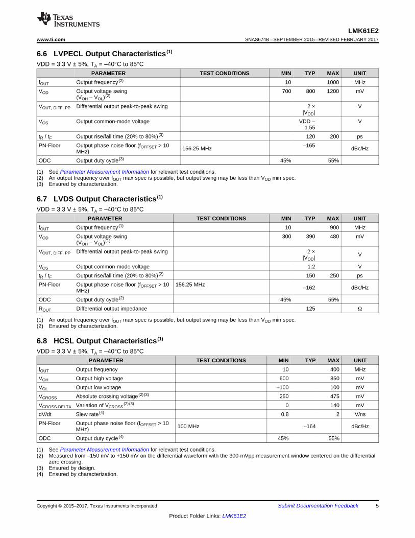
6.6 LVPECL Output Characteristics (1)
VDD = 3.3 V ± 5%, TA = –40°C to 85°CPARAMETER TEST CONDITIONS MIN TYP MAX UNIT
fOUT Output frequency (2) 10 1000 MHzVOD Output voltage swing
(VOH – VOL) (2)700 800 1200 mV
VOUT, DIFF, PP Differential output peak-to-peak swing 2 ×|VOD|
V
VOS Output common-mode voltage VDD –1.55
V
tR / tF Output rise/fall time (20% to 80%) (3) 120 200 psPN-Floor Output phase noise floor (fOFFSET > 10
MHz) 156.25 MHz –165 dBc/Hz
ODC Output duty cycle (3) 45% 55%
(1) An output frequency over fOUT max spec is possible, but output swing may be less than VOD min spec.(2) Ensured by characterization.
6.7 LVDS Output Characteristics (1)
VDD = 3.3 V ± 5%, TA = –40°C to 85°CPARAMETER TEST CONDITIONS MIN TYP MAX UNIT
fOUT Output frequency (1) 10 900 MHzVOD Output voltage swing
(VOH – VOL) (1)300 390 480 mV
VOUT, DIFF, PP Differential output peak-to-peak swing 2 ×|VOD| V
VOS Output common-mode voltage 1.2 VtR / tF Output rise/fall time (20% to 80%) (2) 150 250 psPN-Floor Output phase noise floor (fOFFSET > 10
MHz)156.25 MHz –162 dBc/Hz
ODC Output duty cycle (2) 45% 55%ROUT Differential output impedance 125 Ω
(1) See Parameter Measurement Information for relevant test conditions.(2) Measured from –150 mV to +150 mV on the differential waveform with the 300-mVpp measurement window centered on the differential
zero crossing.(3) Ensured by design.(4) Ensured by characterization.
6.8 HCSL Output Characteristics (1)
VDD = 3.3 V ± 5%, TA = –40°C to 85°CPARAMETER TEST CONDITIONS MIN TYP MAX UNIT
fOUT Output frequency 10 400 MHzVOH Output high voltage 600 850 mVVOL Output low voltage –100 100 mVVCROSS Absolute crossing voltage (2) (3) 250 475 mVVCROSS-DELTA Variation of VCROSS
(2) (3) 0 140 mVdV/dt Slew rate (4) 0.8 2 V/nsPN-Floor Output phase noise floor (fOFFSET > 10
MHz) 100 MHz –164 dBc/Hz
ODC Output duty cycle (4) 45% 55%
6
LMK61E2SNAS674B –SEPTEMBER 2015–REVISED FEBRUARY 2017 www.ti.com
Product Folder Links: LMK61E2
Submit Documentation Feedback Copyright © 2015–2017, Texas Instruments Incorporated
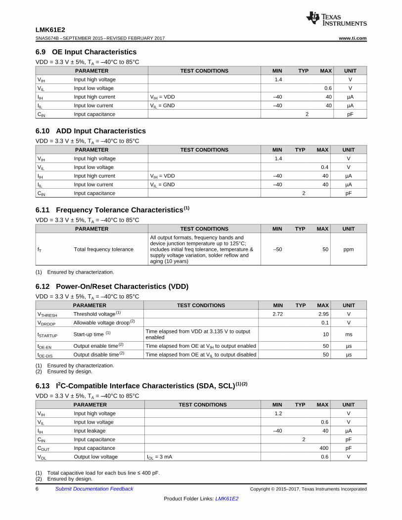
6.9 OE Input CharacteristicsVDD = 3.3 V ± 5%, TA = –40°C to 85°C
PARAMETER TEST CONDITIONS MIN TYP MAX UNITVIH Input high voltage 1.4 VVIL Input low voltage 0.6 VIIH Input high current VIH = VDD –40 40 µAIIL Input low current VIL = GND –40 40 µACIN Input capacitance 2 pF
6.10 ADD Input CharacteristicsVDD = 3.3 V ± 5%, TA = –40°C to 85°C
PARAMETER TEST CONDITIONS MIN TYP MAX UNITVIH Input high voltage 1.4 VVIL Input low voltage 0.4 VIIH Input high current VIH = VDD –40 40 µAIIL Input low current VIL = GND –40 40 µACIN Input capacitance 2 pF
(1) Ensured by characterization.
6.11 Frequency Tolerance Characteristics (1)
VDD = 3.3 V ± 5%, TA = –40°C to 85°CPARAMETER TEST CONDITIONS MIN TYP MAX UNIT
fT Total frequency tolerance
All output formats, frequency bands anddevice junction temperature up to 125°C;includes initial freq tolerance, temperature &supply voltage variation, solder reflow andaging (10 years)
–50 50 ppm
(1) Ensured by characterization.(2) Ensured by design.
6.12 Power-On/Reset Characteristics (VDD)VDD = 3.3 V ± 5%, TA = –40°C to 85°C
PARAMETER TEST CONDITIONS MIN TYP MAX UNITVTHRESH Threshold voltage (1) 2.72 2.95 VVDROOP Allowable voltage droop (2) 0.1 V
tSTARTUP Start-up time (1) Time elapsed from VDD at 3.135 V to outputenabled 10 ms
tOE-EN Output enable time (2) Time elapsed from OE at VIH to output enabled 50 µstOE-DIS Output disable time (2) Time elapsed from OE at VIL to output disabled 50 µs
(1) Total capacitive load for each bus line ≤ 400 pF.(2) Ensured by design.
6.13 I2C-Compatible Interface Characteristics (SDA, SCL) (1) (2)
VDD = 3.3 V ± 5%, TA = –40°C to 85°CPARAMETER TEST CONDITIONS MIN TYP MAX UNIT
VIH Input high voltage 1.2 VVIL Input low voltage 0.6 VIIH Input leakage –40 40 µACIN Input capacitance 2 pFCOUT Input capacitance 400 pFVOL Output low voltage IOL = 3 mA 0.6 V
7
LMK61E2www.ti.com SNAS674B –SEPTEMBER 2015–REVISED FEBRUARY 2017
Product Folder Links: LMK61E2
Submit Documentation FeedbackCopyright © 2015–2017, Texas Instruments Incorporated
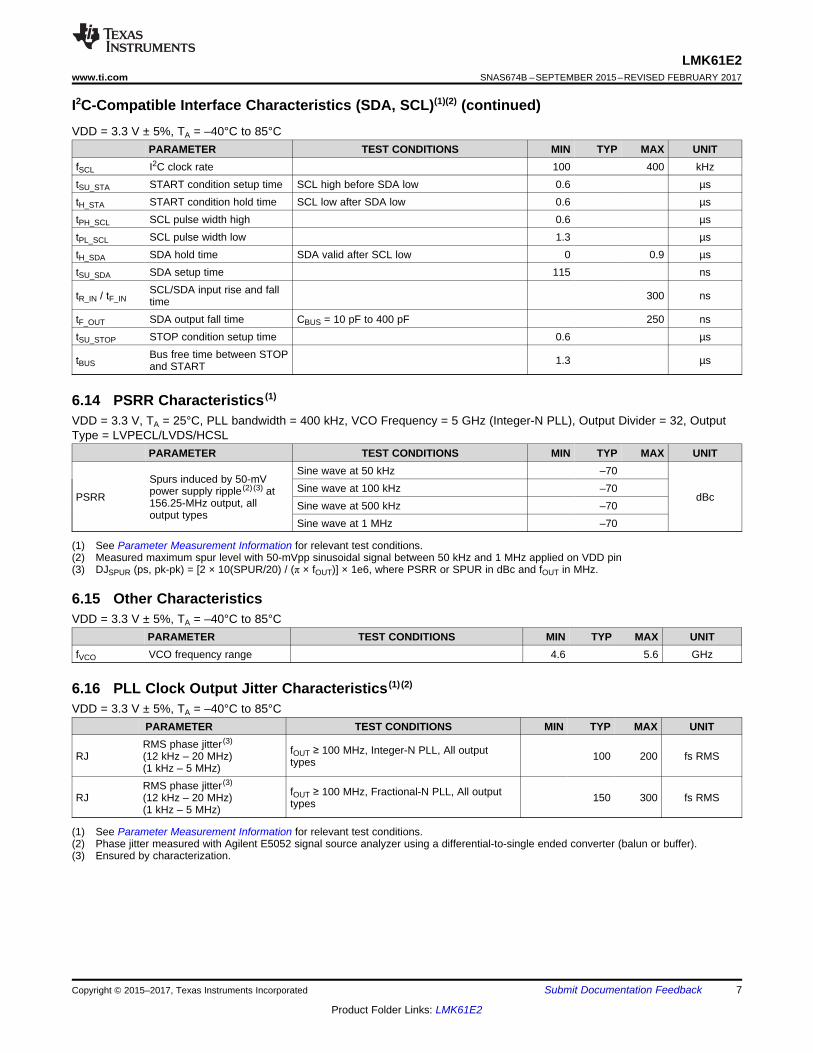
I2C-Compatible Interface Characteristics (SDA, SCL)(1)(2) (continued)VDD = 3.3 V ± 5%, TA = –40°C to 85°C
PARAMETER TEST CONDITIONS MIN TYP MAX UNITfSCL I2C clock rate 100 400 kHztSU_STA START condition setup time SCL high before SDA low 0.6 µstH_STA START condition hold time SCL low after SDA low 0.6 µstPH_SCL SCL pulse width high 0.6 µstPL_SCL SCL pulse width low 1.3 µstH_SDA SDA hold time SDA valid after SCL low 0 0.9 µstSU_SDA SDA setup time 115 ns
tR_IN / tF_INSCL/SDA input rise and falltime 300 ns
tF_OUT SDA output fall time CBUS = 10 pF to 400 pF 250 nstSU_STOP STOP condition setup time 0.6 µs
tBUSBus free time between STOPand START 1.3 µs
(1) See Parameter Measurement Information for relevant test conditions.(2) Measured maximum spur level with 50-mVpp sinusoidal signal between 50 kHz and 1 MHz applied on VDD pin(3) DJSPUR (ps, pk-pk) = [2 × 10(SPUR/20) / (π × fOUT)] × 1e6, where PSRR or SPUR in dBc and fOUT in MHz.
6.14 PSRR Characteristics (1)
VDD = 3.3 V, TA = 25°C, PLL bandwidth = 400 kHz, VCO Frequency = 5 GHz (Integer-N PLL), Output Divider = 32, OutputType = LVPECL/LVDS/HCSL
PARAMETER TEST CONDITIONS MIN TYP MAX UNIT
PSRR
Spurs induced by 50-mVpower supply ripple (2) (3) at156.25-MHz output, alloutput types
Sine wave at 50 kHz –70
dBcSine wave at 100 kHz –70Sine wave at 500 kHz –70Sine wave at 1 MHz –70
6.15 Other CharacteristicsVDD = 3.3 V ± 5%, TA = –40°C to 85°C
PARAMETER TEST CONDITIONS MIN TYP MAX UNITfVCO VCO frequency range 4.6 5.6 GHz
(1) See Parameter Measurement Information for relevant test conditions.(2) Phase jitter measured with Agilent E5052 signal source analyzer using a differential-to-single ended converter (balun or buffer).(3) Ensured by characterization.
6.16 PLL Clock Output Jitter Characteristics (1) (2)
VDD = 3.3 V ± 5%, TA = –40°C to 85°CPARAMETER TEST CONDITIONS MIN TYP MAX UNIT
RJRMS phase jitter (3)
(12 kHz – 20 MHz)(1 kHz – 5 MHz)
fOUT ≥ 100 MHz, Integer-N PLL, All outputtypes 100 200 fs RMS
RJRMS phase jitter (3)
(12 kHz – 20 MHz)(1 kHz – 5 MHz)
fOUT ≥ 100 MHz, Fractional-N PLL, All outputtypes 150 300 fs RMS
8
LMK61E2SNAS674B –SEPTEMBER 2015–REVISED FEBRUARY 2017 www.ti.com
Product Folder Links: LMK61E2
Submit Documentation Feedback Copyright © 2015–2017, Texas Instruments Incorporated
(1) See Parameter Measurement Information for relevant test conditions.(2) Phase jitter measured with Agilent E5052 signal source analyzer using a differential-to-single ended converter (balun or buffer).
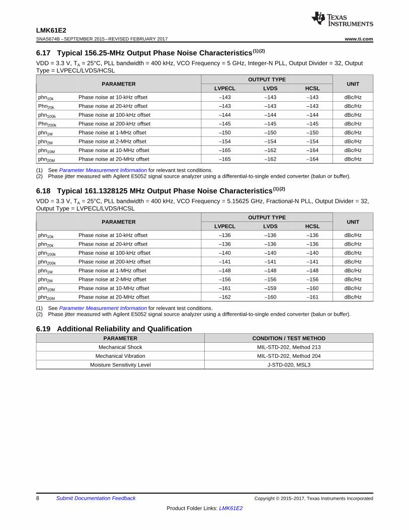
6.17 Typical 156.25-MHz Output Phase Noise Characteristics (1) (2)
VDD = 3.3 V, TA = 25°C, PLL bandwidth = 400 kHz, VCO Frequency = 5 GHz, Integer-N PLL, Output Divider = 32, OutputType = LVPECL/LVDS/HCSL
PARAMETEROUTPUT TYPE
UNITLVPECL LVDS HCSL
phn10k Phase noise at 10-kHz offset –143 –143 –143 dBc/HzPhn20k Phase noise at 20-kHz offset –143 –143 –143 dBc/Hzphn100k Phase noise at 100-kHz offset –144 –144 –144 dBc/HzPhn200k Phase noise at 200-kHz offset –145 –145 –145 dBc/Hzphn1M Phase noise at 1-MHz offset –150 –150 –150 dBc/Hzphn2M Phase noise at 2-MHz offset –154 –154 –154 dBc/Hzphn10M Phase noise at 10-MHz offset –165 –162 –164 dBc/Hzphn20M Phase noise at 20-MHz offset –165 –162 –164 dBc/Hz
(1) See Parameter Measurement Information for relevant test conditions.(2) Phase jitter measured with Agilent E5052 signal source analyzer using a differential-to-single ended converter (balun or buffer).
6.18 Typical 161.1328125 MHz Output Phase Noise Characteristics (1) (2)
VDD = 3.3 V, TA = 25°C, PLL bandwidth = 400 kHz, VCO Frequency = 5.15625 GHz, Fractional-N PLL, Output Divider = 32,Output Type = LVPECL/LVDS/HCSL
PARAMETEROUTPUT TYPE
UNITLVPECL LVDS HCSL
phn10k Phase noise at 10-kHz offset –136 –136 –136 dBc/Hzphn20k Phase noise at 20-kHz offset –136 –136 –136 dBc/Hzphn100k Phase noise at 100-kHz offset –140 –140 –140 dBc/Hzphn200k Phase noise at 200-kHz offset –141 –141 –141 dBc/Hzphn1M Phase noise at 1-MHz offset –148 –148 –148 dBc/Hzphn2M Phase noise at 2-MHz offset –156 –156 –156 dBc/Hzphn10M Phase noise at 10-MHz offset –161 –159 –160 dBc/Hzphn20M Phase noise at 20-MHz offset –162 –160 –161 dBc/Hz
6.19 Additional Reliability and QualificationPARAMETER CONDITION / TEST METHOD
Mechanical Shock MIL-STD-202, Method 213Mechanical Vibration MIL-STD-202, Method 204
Moisture Sensitivity Level J-STD-020, MSL3
9
LMK61E2www.ti.com SNAS674B –SEPTEMBER 2015–REVISED FEBRUARY 2017
Product Folder Links: LMK61E2
Submit Documentation FeedbackCopyright © 2015–2017, Texas Instruments Incorporated
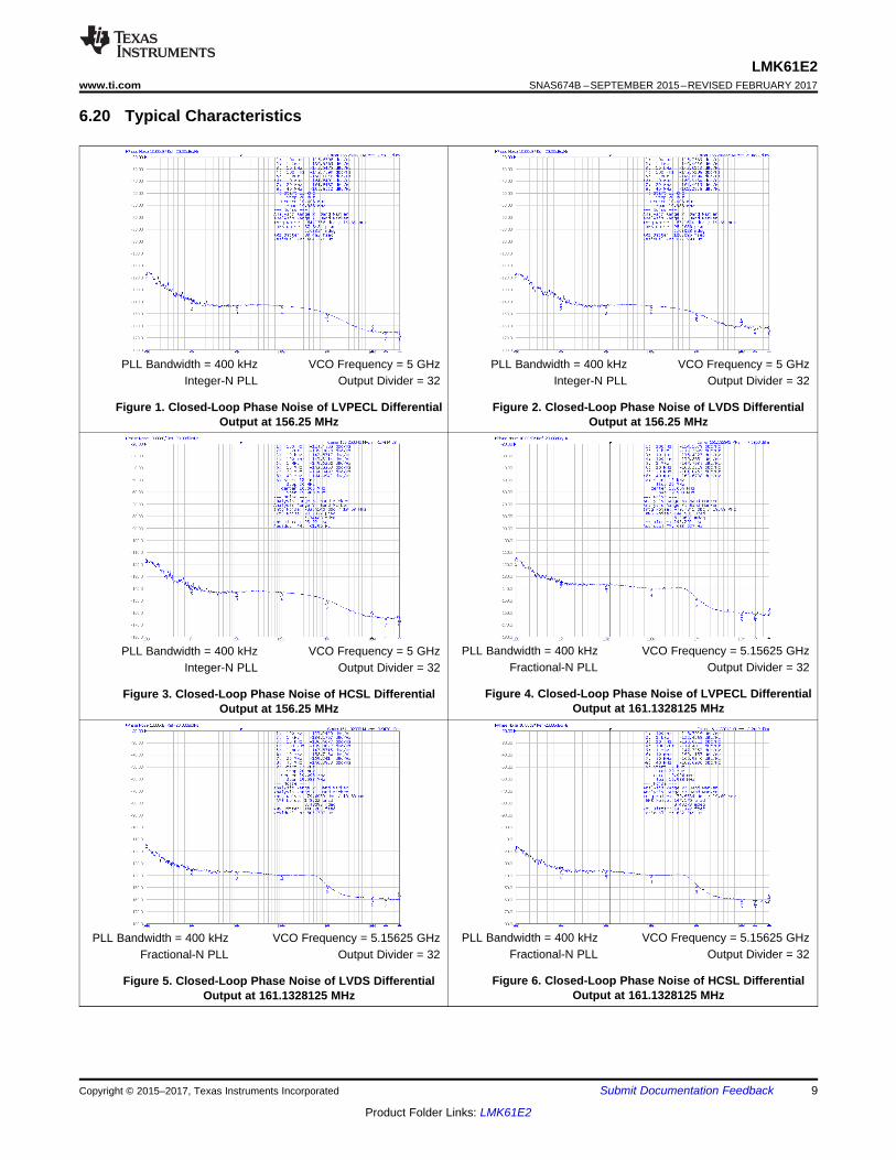
6.20 Typical Characteristics
PLL Bandwidth = 400 kHz VCO Frequency = 5 GHzInteger-N PLL Output Divider = 32
Figure 1. Closed-Loop Phase Noise of LVPECL DifferentialOutput at 156.25 MHz
PLL Bandwidth = 400 kHz VCO Frequency = 5 GHzInteger-N PLL Output Divider = 32
Figure 2. Closed-Loop Phase Noise of LVDS DifferentialOutput at 156.25 MHz
PLL Bandwidth = 400 kHz VCO Frequency = 5 GHzInteger-N PLL Output Divider = 32
Figure 3. Closed-Loop Phase Noise of HCSL DifferentialOutput at 156.25 MHz
PLL Bandwidth = 400 kHz VCO Frequency = 5.15625 GHzFractional-N PLL Output Divider = 32
Figure 4. Closed-Loop Phase Noise of LVPECL DifferentialOutput at 161.1328125 MHz
PLL Bandwidth = 400 kHz VCO Frequency = 5.15625 GHzFractional-N PLL Output Divider = 32
Figure 5. Closed-Loop Phase Noise of LVDS DifferentialOutput at 161.1328125 MHz
PLL Bandwidth = 400 kHz VCO Frequency = 5.15625 GHzFractional-N PLL Output Divider = 32
Figure 6. Closed-Loop Phase Noise of HCSL DifferentialOutput at 161.1328125 MHz
Frequency (MHz)
Am
plitu
de (
dBm
)
80 100 120 140 160 180 200 220 240-100
-90
-80
-70
-60
-50
-40
-30
-20
-10
0
10
D011Frequency (MHz)
Am
plitu
de (
dBm
)
80 100 120 140 160 180 200 220 240-100
-90
-80
-70
-60
-50
-40
-30
-20
-10
0
10
D012
Frequency (MHz)
Am
plitu
de (
dBm
)
78.125 109.375 140.625 171.875 203.125 234.375-90
-80
-70
-60
-50
-40
-30
-20
-10
0
10
D009Frequency (MHz)
Am
plitu
de (
dBm
)
80 100 120 140 160 180 200 220 240-100
-90
-80
-70
-60
-50
-40
-30
-20
-10
0
10
D010
Frequency (MHz)
Am
plitu
de (
dBm
)
78.125 109.375 140.625 171.875 203.125 234.375-90
-80
-70
-60
-50
-40
-30
-20
-10
0
10
D007Frequency (MHz)
Am
plitu
de (
dBm
)
78.125 109.375 140.625 171.875 203.125 234.375-90
-80
-70
-60
-50
-40
-30
-20
-10
0
10
D008
10
LMK61E2SNAS674B –SEPTEMBER 2015–REVISED FEBRUARY 2017 www.ti.com
Product Folder Links: LMK61E2
Submit Documentation Feedback Copyright © 2015–2017, Texas Instruments Incorporated
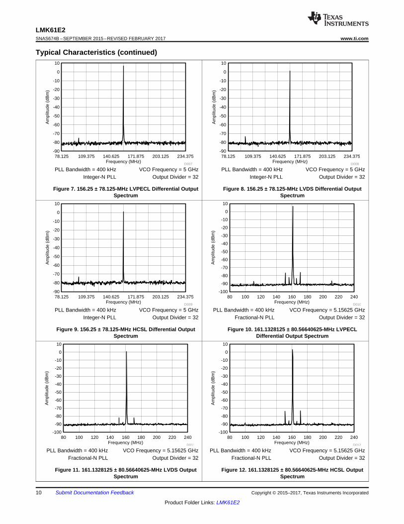
Typical Characteristics (continued)
PLL Bandwidth = 400 kHz VCO Frequency = 5 GHzInteger-N PLL Output Divider = 32
Figure 7. 156.25 ± 78.125-MHz LVPECL Differential OutputSpectrum
PLL Bandwidth = 400 kHz VCO Frequency = 5 GHzInteger-N PLL Output Divider = 32
Figure 8. 156.25 ± 78.125-MHz LVDS Differential OutputSpectrum
PLL Bandwidth = 400 kHz VCO Frequency = 5 GHzInteger-N PLL Output Divider = 32
Figure 9. 156.25 ± 78.125-MHz HCSL Differential OutputSpectrum
PLL Bandwidth = 400 kHz VCO Frequency = 5.15625 GHzFractional-N PLL Output Divider = 32
Figure 10. 161.1328125 ± 80.56640625-MHz LVPECLDifferential Output Spectrum
PLL Bandwidth = 400 kHz VCO Frequency = 5.15625 GHzFractional-N PLL Output Divider = 32
Figure 11. 161.1328125 ± 80.56640625-MHz LVDS OutputSpectrum
PLL Bandwidth = 400 kHz VCO Frequency = 5.15625 GHzFractional-N PLL Output Divider = 32
Figure 12. 161.1328125 ± 80.56640625-MHz HCSL OutputSpectrum
Output Frequency (MHz)
Out
put D
iffer
entia
l Sw
ing
(Vp-
p)
0 100 200 300 400 5001.4
1.42
1.44
1.46
1.48
1.5
D015
Output Frequency (MHz)
Out
put D
iffer
entia
l Sw
ing
(Vp-
p)
0 200 400 600 800 10001.1
1.2
1.3
1.4
1.5
1.6
1.7
1.8
D013Output Frequency (MHz)
Out
put D
iffer
entia
l Sw
ing
(Vp-
p)
0 200 400 600 800 10000.5
0.6
0.7
0.8
0.9
D014
11
LMK61E2www.ti.com SNAS674B –SEPTEMBER 2015–REVISED FEBRUARY 2017
Product Folder Links: LMK61E2
Submit Documentation FeedbackCopyright © 2015–2017, Texas Instruments Incorporated
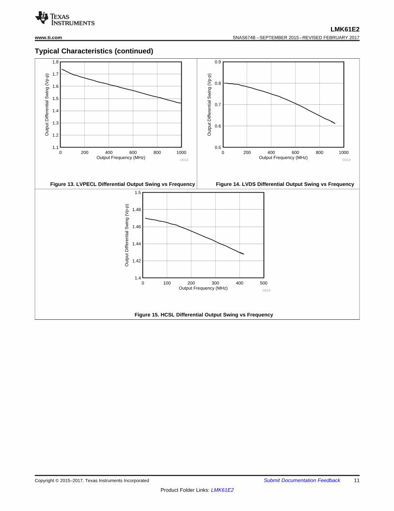
Typical Characteristics (continued)
Figure 13. LVPECL Differential Output Swing vs Frequency Figure 14. LVDS Differential Output Swing vs Frequency
Figure 15. HCSL Differential Output Swing vs Frequency
Phase Noise/SpectrumAnalyzer
LVDSBalun/Buffer
LMK61E2
LMK61E2 LVPECL
150 150
Balun/Buffer
Phase Noise/SpectrumAnalyzer
LMK61E2 HCSL
50 50
Oscilloscope
High impedance differential probe
LMK61E2 LVDS Oscilloscope
High impedance differential probe
LMK61E2 LVPECL
150 150
Oscilloscope
High impedance differential probe
12
LMK61E2SNAS674B –SEPTEMBER 2015–REVISED FEBRUARY 2017 www.ti.com
Product Folder Links: LMK61E2
Submit Documentation Feedback Copyright © 2015–2017, Texas Instruments Incorporated
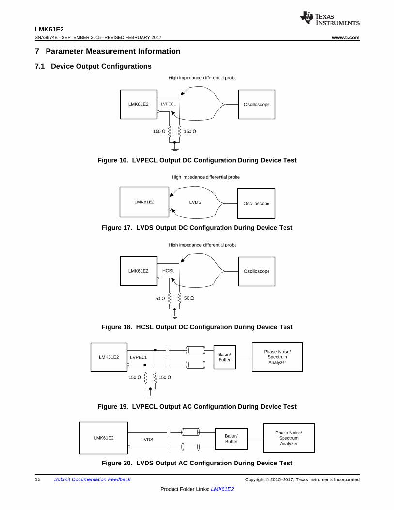
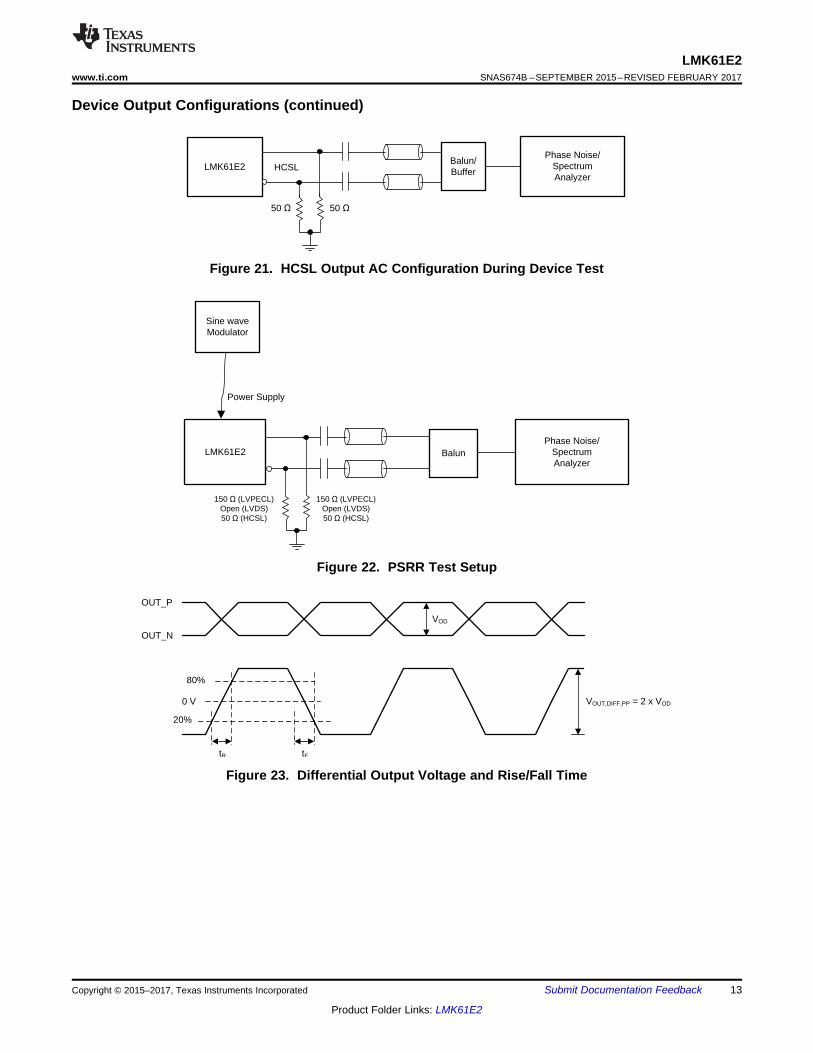
7 Parameter Measurement Information
7.1 Device Output Configurations
Figure 16. LVPECL Output DC Configuration During Device Test
Figure 17. LVDS Output DC Configuration During Device Test
Figure 18. HCSL Output DC Configuration During Device Test
Figure 19. LVPECL Output AC Configuration During Device Test
Figure 20. LVDS Output AC Configuration During Device Test
VOD
OUT_P
OUT_N
VOUT,DIFF,PP = 2 x VOD0 V
20%
80%
tR tF
Sine wave Modulator
Power Supply
BalunPhase Noise/
SpectrumAnalyzer
LMK61E2
150 �(LVPECL)Open (LVDS)50 �(HCSL)
150 �(LVPECL)Open (LVDS)50 �(HCSL)
LMK61E2 HCSL
50 50
Balun/Buffer
Phase Noise/SpectrumAnalyzer
13
LMK61E2www.ti.com SNAS674B –SEPTEMBER 2015–REVISED FEBRUARY 2017
Product Folder Links: LMK61E2
Submit Documentation FeedbackCopyright © 2015–2017, Texas Instruments Incorporated
Device Output Configurations (continued)
Figure 21. HCSL Output AC Configuration During Device Test
Figure 22. PSRR Test Setup
Figure 23. Differential Output Voltage and Rise/Fall Time
Output
Control
Power Conditioning
VDD
od
EEPROMRegistersodSCL
LVPECL or LVDS or HCSL
SDA
od = open-drain
PLL
VCO: 4.6 GHz ~ 5.6 GHz
¥
10 nF
Device Control3ADD
Integrated Oscillator
XO
N Div
�û�fractional
3 = tri-state
Integer Div/5 - /511
GND
OE
Copyright © 2016, Texas Instruments Incorporated
14
LMK61E2SNAS674B –SEPTEMBER 2015–REVISED FEBRUARY 2017 www.ti.com
Product Folder Links: LMK61E2
Submit Documentation Feedback Copyright © 2015–2017, Texas Instruments Incorporated
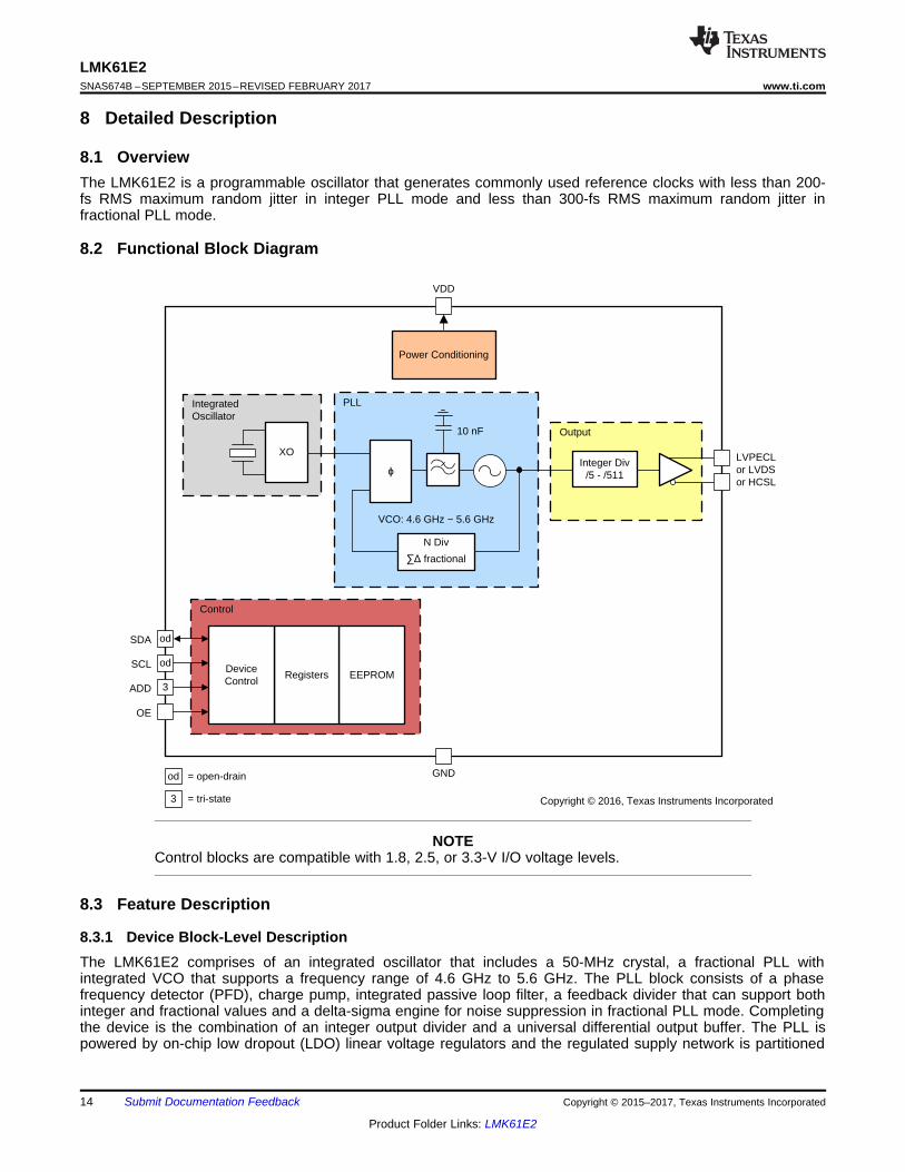
8 Detailed Description
8.1 OverviewThe LMK61E2 is a programmable oscillator that generates commonly used reference clocks with less than 200-fs RMS maximum random jitter in integer PLL mode and less than 300-fs RMS maximum random jitter infractional PLL mode.
8.2 Functional Block Diagram
NOTEControl blocks are compatible with 1.8, 2.5, or 3.3-V I/O voltage levels.
8.3 Feature Description
8.3.1 Device Block-Level DescriptionThe LMK61E2 comprises of an integrated oscillator that includes a 50-MHz crystal, a fractional PLL withintegrated VCO that supports a frequency range of 4.6 GHz to 5.6 GHz. The PLL block consists of a phasefrequency detector (PFD), charge pump, integrated passive loop filter, a feedback divider that can support bothinteger and fractional values and a delta-sigma engine for noise suppression in fractional PLL mode. Completingthe device is the combination of an integer output divider and a universal differential output buffer. The PLL ispowered by on-chip low dropout (LDO) linear voltage regulators and the regulated supply network is partitioned
5 4 3 2
Reg5Register Number (s)
Bit Number (s)
R5.2
15
LMK61E2www.ti.com SNAS674B –SEPTEMBER 2015–REVISED FEBRUARY 2017
Product Folder Links: LMK61E2
Submit Documentation FeedbackCopyright © 2015–2017, Texas Instruments Incorporated
Feature Description (continued)such that the sensitive analog supplies are running from separate LDOs than the digital supplies which use theirown LDO. The LDOs provide isolation to the PLL from any noise in the external power supply rail with a PSRR ofbetter than –70 dBc at 50-kHz to 1-MHz ripple frequencies at 3.3-V device supply. The device supports fine andcoarse frequency margining by changing the settings of the integrated oscillator and the output dividerrespectively.
8.3.2 Device Configuration ControlThe LMK61E2 supports I2C programming interface where an I2C host can update any device configuration afterthe device enables the host interface and the host writes a sequence that updates the device registers. Once thedevice configuration is set, the host can also write to the on-chip EEPROM for a new set of power-up defaultsbased on the configuration pin settings in the soft pin configuration mode.
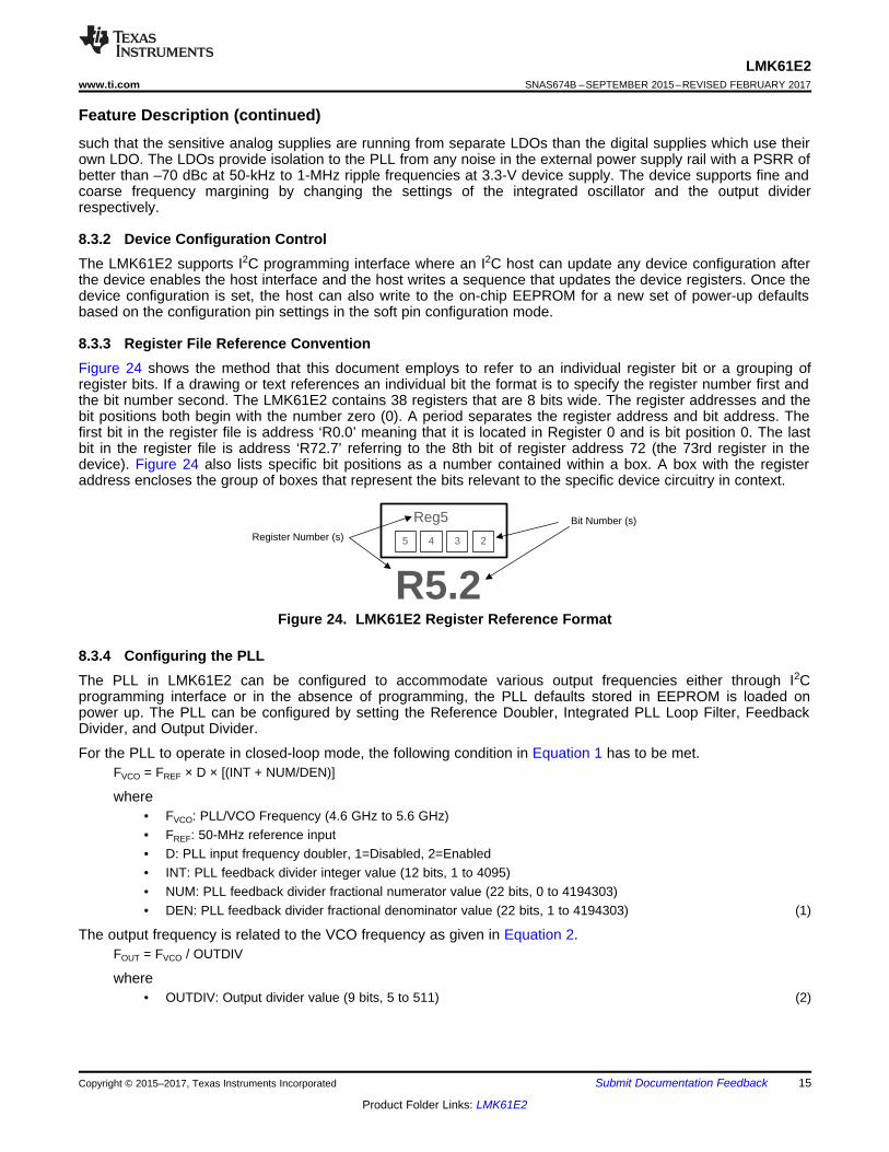
8.3.3 Register File Reference ConventionFigure 24 shows the method that this document employs to refer to an individual register bit or a grouping ofregister bits. If a drawing or text references an individual bit the format is to specify the register number first andthe bit number second. The LMK61E2 contains 38 registers that are 8 bits wide. The register addresses and thebit positions both begin with the number zero (0). A period separates the register address and bit address. Thefirst bit in the register file is address ‘R0.0’ meaning that it is located in Register 0 and is bit position 0. The lastbit in the register file is address ‘R72.7’ referring to the 8th bit of register address 72 (the 73rd register in thedevice). Figure 24 also lists specific bit positions as a number contained within a box. A box with the registeraddress encloses the group of boxes that represent the bits relevant to the specific device circuitry in context.
Figure 24. LMK61E2 Register Reference Format
8.3.4 Configuring the PLLThe PLL in LMK61E2 can be configured to accommodate various output frequencies either through I2Cprogramming interface or in the absence of programming, the PLL defaults stored in EEPROM is loaded onpower up. The PLL can be configured by setting the Reference Doubler, Integrated PLL Loop Filter, FeedbackDivider, and Output Divider.
For the PLL to operate in closed-loop mode, the following condition in Equation 1 has to be met.FVCO = FREF × D × [(INT + NUM/DEN)]
where• FVCO: PLL/VCO Frequency (4.6 GHz to 5.6 GHz)• FREF: 50-MHz reference input• D: PLL input frequency doubler, 1=Disabled, 2=Enabled• INT: PLL feedback divider integer value (12 bits, 1 to 4095)• NUM: PLL feedback divider fractional numerator value (22 bits, 0 to 4194303)• DEN: PLL feedback divider fractional denominator value (22 bits, 1 to 4194303) (1)
The output frequency is related to the VCO frequency as given in Equation 2.FOUT = FVCO / OUTDIV
where• OUTDIV: Output divider value (9 bits, 5 to 511) (2)
16
LMK61E2SNAS674B –SEPTEMBER 2015–REVISED FEBRUARY 2017 www.ti.com
Product Folder Links: LMK61E2
Submit Documentation Feedback Copyright © 2015–2017, Texas Instruments Incorporated
Feature Description (continued)8.3.5 Integrated OscillatorThe integrated oscillator in LMK61E2 features programmable load capacitances that can be set to either operateat exactly its nominal oscillation frequency or operate at a fixed frequency offset from its nominal oscillationfrequency. This is done by programming R16 and R17. More details on frequency margining are provided in FineFrequency Margining.
8.3.6 Reference DoublerThe reference path has a frequency doubler that can be enabled by programming R34.5 = 1. Enabling thedoubler allows a higher comparison frequency for the PLL and would result in a 3-dB reduction in the in-bandphase noise at the output of the LMK61E2. Enabling the doubler also results in higher reference and phasedetector spurs which will be minimized by enabling the higher order components (R3, C3) of the loop filter andprogrammed to appropriate values. Disabling the doubler would result in higher in-band phase noise on thedevice output than when the doubler is enabled but the reference and phase detector spurs would be lower onthe device output than when the doubler is enabled.
8.3.7 Phase Frequency DetectorThe Phase Frequency Detector (PFD) of the PLL takes inputs from the reference path and the feedback divideroutput and produces an output that is dependent on the phase and frequency difference between the two inputs.The input frequency of the PFD is 50 MHz when reference doubler is disabled, or 100 MHz when referencedoubler is enabled.
8.3.8 Feedback Divider (N)The N divider of the PLL includes fractional compensation and can achieve any fractional denominator (DEN)from 1 to 4,194,303. The integer portion, INT, is the whole part of the N divider value and the fractional portion,NUM / DEN, is the remaining fraction. INT, NUM, and DEN are programmed in R25, R26, R27, R28, R29, R30,R31, and R32. The total programmed N divider value, N, is determined by: N = INT + NUM / DEN. The output ofthe N divider sets the PFD frequency to the PLL and should equal 50 MHz, when reference doubler is disabled,or 100 MHz, when reference doubler is enabled.
8.3.9 Fractional CircuitryThe delta signal modulator is a key component of the fractional circuitry and is involved in noise shaping forbetter phase noise and spurs in the band of interest. The order of the delta sigma modulator is selectablebetween integer mode and third order, for fractional PLL mode, and can be programmed in R33[1-0]. Ditheringcan be programmed in R33[3-2] and should be disabled for integer PLL mode and set to weak for fractional PLLmode.
8.3.10 Charge PumpThe PLL has charge pump slices of 1.6 mA, to be used when PLL is set to fractional mode, or 6.4 mA, to beused when PLL is set to integer mode. These slices can be selected by programming R34[3-0]. When PLL is setto fractional mode, a phase shift needs to be introduced to maintain a linear response and ensure consistentperformance across operating conditions and a value of 0x2 should be programmed in R35[6-4]. When PLL isset to integer mode, a value of 0x0 should be programmed in R35[6-4].
8.3.11 Loop FilterThe LMK61E2 features a fully integrated loop filter for the PLL and supports programmable loop bandwidth from100 kHz to 1 MHz. The loop filter components, R2, C1, R3, and C3 can be configured by programming R36,R37, R38, and R39 respectively. The LMK61E2 features a fixed value of C2 of 10 nF. When PLL is configured inthe fractional mode, R35.2 should be set to 1. When reference doubler is disabled for integer mode PLL, R35.2should be set to 0 and R38[6-0] should be set to 0x00. When reference doubler is enabled for integer mode PLL,R35.2 should be set to 1 and R38 and R39 are written with the appropriate values. Figure 25 shows the loopfilter structure of the PLL. It is important to set the PLL to best possible bandwidth to minimize output jitter. TIprovides the WEBENCH® Clock Architect Tool that makes it easy to select the right loop filter components.
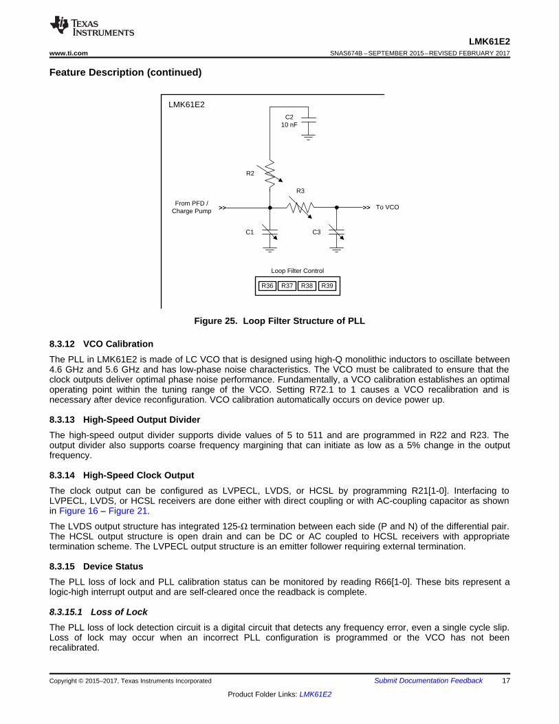
R2
C1
R3
C3
From PFD / Charge Pump >> >>
LMK61E2
R36 R37 R38 R39
Loop Filter Control
C210 nF
To VCO
17
LMK61E2www.ti.com SNAS674B –SEPTEMBER 2015–REVISED FEBRUARY 2017
Product Folder Links: LMK61E2
Submit Documentation FeedbackCopyright © 2015–2017, Texas Instruments Incorporated
Feature Description (continued)
Figure 25. Loop Filter Structure of PLL
8.3.12 VCO CalibrationThe PLL in LMK61E2 is made of LC VCO that is designed using high-Q monolithic inductors to oscillate between4.6 GHz and 5.6 GHz and has low-phase noise characteristics. The VCO must be calibrated to ensure that theclock outputs deliver optimal phase noise performance. Fundamentally, a VCO calibration establishes an optimaloperating point within the tuning range of the VCO. Setting R72.1 to 1 causes a VCO recalibration and isnecessary after device reconfiguration. VCO calibration automatically occurs on device power up.
8.3.13 High-Speed Output DividerThe high-speed output divider supports divide values of 5 to 511 and are programmed in R22 and R23. Theoutput divider also supports coarse frequency margining that can initiate as low as a 5% change in the outputfrequency.
8.3.14 High-Speed Clock OutputThe clock output can be configured as LVPECL, LVDS, or HCSL by programming R21[1-0]. Interfacing toLVPECL, LVDS, or HCSL receivers are done either with direct coupling or with AC-coupling capacitor as shownin Figure 16 – Figure 21.
The LVDS output structure has integrated 125-Ω termination between each side (P and N) of the differential pair.The HCSL output structure is open drain and can be DC or AC coupled to HCSL receivers with appropriatetermination scheme. The LVPECL output structure is an emitter follower requiring external termination.
8.3.15 Device StatusThe PLL loss of lock and PLL calibration status can be monitored by reading R66[1-0]. These bits represent alogic-high interrupt output and are self-cleared once the readback is complete.
8.3.15.1 Loss of LockThe PLL loss of lock detection circuit is a digital circuit that detects any frequency error, even a single cycle slip.Loss of lock may occur when an incorrect PLL configuration is programmed or the VCO has not beenrecalibrated.
Device Registers
DeviceHardware
EEPROM SRAM
SCL
SDA
I2CPort
Control/Status Pins
DeviceControl
AndStatus
OE
ADD
Reg 0
Reg1
Reg2
Reg3
Reg32
Reg33
Reg34
Reg35
7 6 5 4 3 2 1 0
7 6 5 4 3 2 1 0
7 6 5 4 3 2 1 0
7 6 5 4 3 2 1 0
7 6 5 4 3 2 1 0
7 6 5 4 3 2 1 0
7 6 5 4 3 2 1 0
7 6 5 4 3 2 1 0
Reg 0
Reg1
Reg2
Reg3
Reg32
Reg33
Reg34
Reg35
7 6 5 4 3 2 1 0
7 6 5 4 3 2 1 0
7 6 5 4 3 2 1 0
7 6 5 4 3 2 1 0
7 6 5 4 3 2 1 0
7 6 5 4 3 2 1 0
7 6 5 4 3 2 1 0
7 6 5 4 3 2 1 0
Reg 0
Reg1
Reg2
Reg3
Reg53
Reg56
Reg66
Reg72
7 6 5 4 3 2 1 0
7 6 5 4 3 2 1 0
7 6 5 4 3 2 1 0
7 6 5 4 3 2 1 0
7 6 5 4 3 2 1 0
7 6 5 4 3 2 1 0
7 6 5 4 3 2 1 0
7 6 5 4 3 2 1 0
18
LMK61E2SNAS674B –SEPTEMBER 2015–REVISED FEBRUARY 2017 www.ti.com
Product Folder Links: LMK61E2
Submit Documentation Feedback Copyright © 2015–2017, Texas Instruments Incorporated
8.4 Device Functional Modes
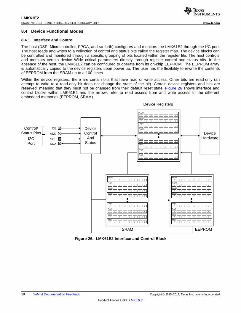
8.4.1 Interface and ControlThe host (DSP, Microcontroller, FPGA, and so forth) configures and monitors the LMK61E2 through the I2C port.The host reads and writes to a collection of control and status bits called the register map. The device blocks canbe controlled and monitored through a specific grouping of bits located within the register file. The host controlsand monitors certain device Wide critical parameters directly through register control and status bits. In theabsence of the host, the LMK61E2 can be configured to operate from its on-chip EEPROM. The EEPROM arrayis automatically copied to the device registers upon power up. The user has the flexibility to rewrite the contentsof EEPROM from the SRAM up to a 100 times.
Within the device registers, there are certain bits that have read or write access. Other bits are read-only (anattempt to write to a read-only bit does not change the state of the bit). Certain device registers and bits arereserved, meaning that they must not be changed from their default reset state. Figure 26 shows interface andcontrol blocks within LMK61E2 and the arrows refer to read access from and write access to the differentembedded memories (EEPROM, SRAM).
Figure 26. LMK61E2 Interface and Control Block
8 8
REGISTER ADDRESS DATA BYTE
I2C PROTOCOL
1
W/R
7
A6 A5 A4 A3 A2 A1 A0
I2C ADDRESS
STOP
~ ~
START STOP
~ ~
~ ~ ~ ~~ ~
tBUS
tSU(START)
SDA
SCL
th(START)tr(SM)
tSU(SDATA)
tW(SCLL) tW(SCLH)
th(SDATA)
tr(SM) tf(SM)
tf(SM) tSU(STOP)
VIH(SM)
VIL(SM)
VIH(SM)
VIL(SM)
ACK
19
LMK61E2www.ti.com SNAS674B –SEPTEMBER 2015–REVISED FEBRUARY 2017
Product Folder Links: LMK61E2
Submit Documentation FeedbackCopyright © 2015–2017, Texas Instruments Incorporated
(1) Total capacitive load for each bus line ≤ 400 pF.(2) Ensured by design.
8.5 Programming
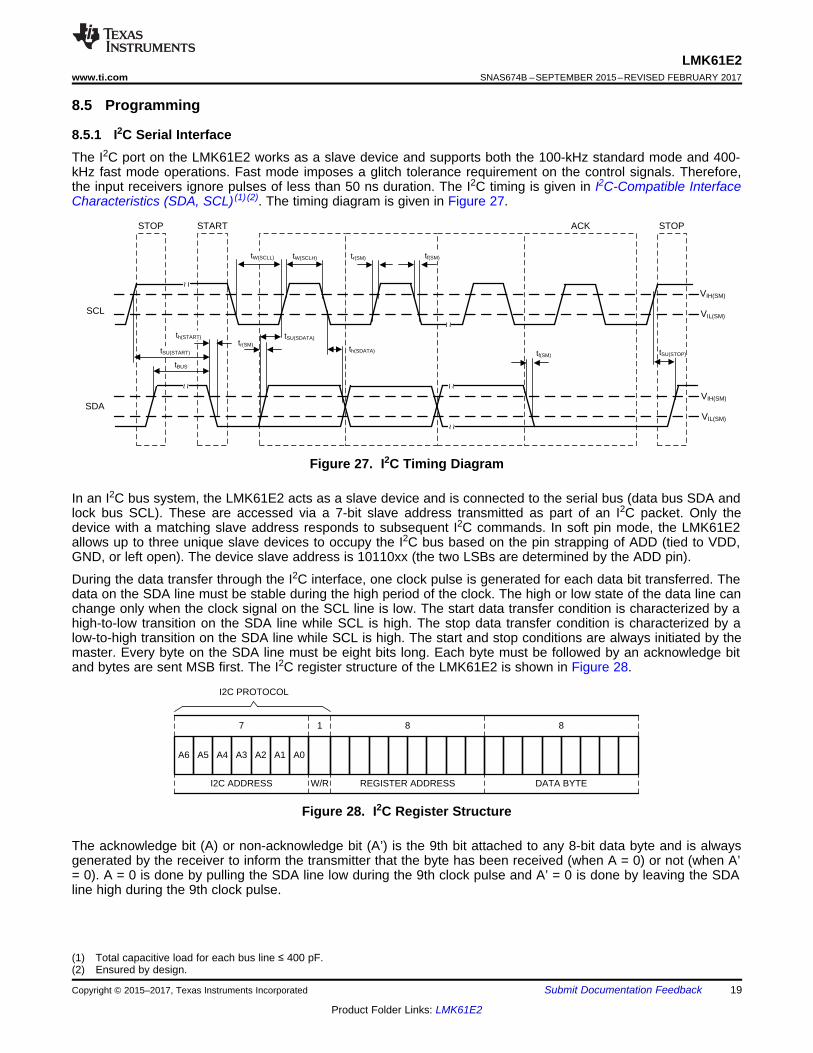
8.5.1 I2C Serial InterfaceThe I2C port on the LMK61E2 works as a slave device and supports both the 100-kHz standard mode and 400-kHz fast mode operations. Fast mode imposes a glitch tolerance requirement on the control signals. Therefore,the input receivers ignore pulses of less than 50 ns duration. The I2C timing is given in I2C-Compatible InterfaceCharacteristics (SDA, SCL) (1) (2). The timing diagram is given in Figure 27.
Figure 27. I2C Timing Diagram
In an I2C bus system, the LMK61E2 acts as a slave device and is connected to the serial bus (data bus SDA andlock bus SCL). These are accessed via a 7-bit slave address transmitted as part of an I2C packet. Only thedevice with a matching slave address responds to subsequent I2C commands. In soft pin mode, the LMK61E2allows up to three unique slave devices to occupy the I2C bus based on the pin strapping of ADD (tied to VDD,GND, or left open). The device slave address is 10110xx (the two LSBs are determined by the ADD pin).
During the data transfer through the I2C interface, one clock pulse is generated for each data bit transferred. Thedata on the SDA line must be stable during the high period of the clock. The high or low state of the data line canchange only when the clock signal on the SCL line is low. The start data transfer condition is characterized by ahigh-to-low transition on the SDA line while SCL is high. The stop data transfer condition is characterized by alow-to-high transition on the SDA line while SCL is high. The start and stop conditions are always initiated by themaster. Every byte on the SDA line must be eight bits long. Each byte must be followed by an acknowledge bitand bytes are sent MSB first. The I2C register structure of the LMK61E2 is shown in Figure 28.
Figure 28. I2C Register Structure
The acknowledge bit (A) or non-acknowledge bit (A’) is the 9th bit attached to any 8-bit data byte and is alwaysgenerated by the receiver to inform the transmitter that the byte has been received (when A = 0) or not (when A’= 0). A = 0 is done by pulling the SDA line low during the 9th clock pulse and A’ = 0 is done by leaving the SDAline high during the 9th clock pulse.
Slave AddressS Wr A CommandCode A
AData Byte 0 ... A PData Byte N-1
1 7
8
1 1 8 1
1 8 1 1
Slave AddressS R/W A Data Byte A P1 7 1 1 8 1 1
MSB LSB MSB LSB
S
Sr
A
R/W
P
Start Condition
Repeated Start Condition
1 = Read (Rd) from slave; 0 = Write (Wr) to slave
Acknowledge (ACK = 0 and NACK = 1)
Stop Condition
Master to Slave Transmission
Slave to Master Transmission
20
LMK61E2SNAS674B –SEPTEMBER 2015–REVISED FEBRUARY 2017 www.ti.com
Product Folder Links: LMK61E2
Submit Documentation Feedback Copyright © 2015–2017, Texas Instruments Incorporated
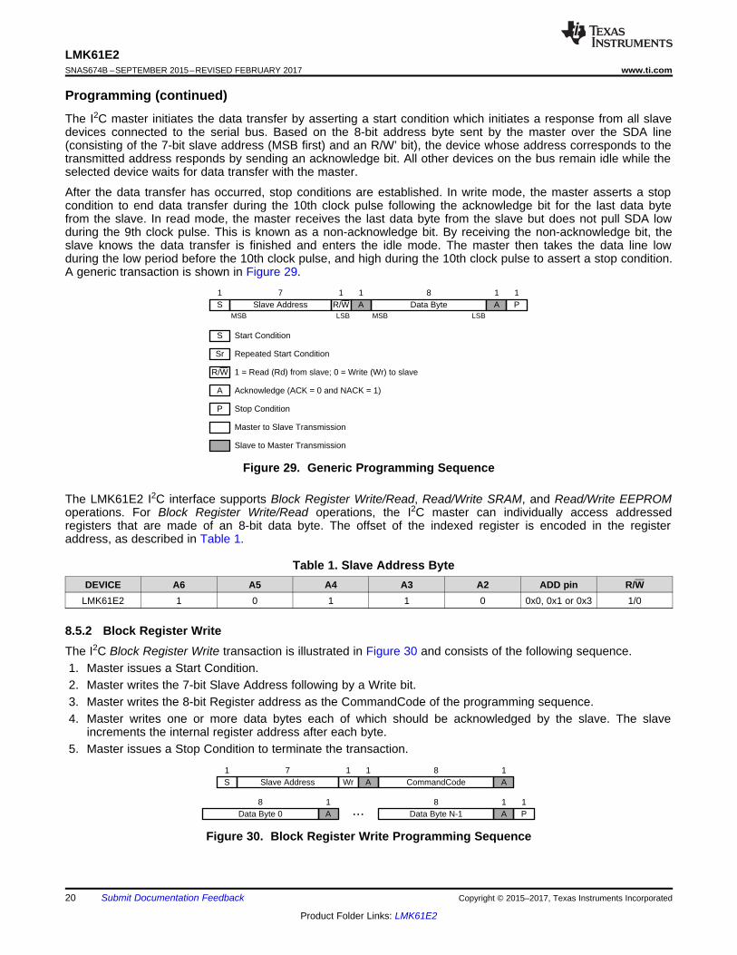
Programming (continued)The I2C master initiates the data transfer by asserting a start condition which initiates a response from all slavedevices connected to the serial bus. Based on the 8-bit address byte sent by the master over the SDA line(consisting of the 7-bit slave address (MSB first) and an R/W’ bit), the device whose address corresponds to thetransmitted address responds by sending an acknowledge bit. All other devices on the bus remain idle while theselected device waits for data transfer with the master.
After the data transfer has occurred, stop conditions are established. In write mode, the master asserts a stopcondition to end data transfer during the 10th clock pulse following the acknowledge bit for the last data bytefrom the slave. In read mode, the master receives the last data byte from the slave but does not pull SDA lowduring the 9th clock pulse. This is known as a non-acknowledge bit. By receiving the non-acknowledge bit, theslave knows the data transfer is finished and enters the idle mode. The master then takes the data line lowduring the low period before the 10th clock pulse, and high during the 10th clock pulse to assert a stop condition.A generic transaction is shown in Figure 29.
Figure 29. Generic Programming Sequence
The LMK61E2 I2C interface supports Block Register Write/Read, Read/Write SRAM, and Read/Write EEPROMoperations. For Block Register Write/Read operations, the I2C master can individually access addressedregisters that are made of an 8-bit data byte. The offset of the indexed register is encoded in the registeraddress, as described in Table 1.
Table 1. Slave Address ByteDEVICE A6 A5 A4 A3 A2 ADD pin R/W
LMK61E2 1 0 1 1 0 0x0, 0x1 or 0x3 1/0
8.5.2 Block Register WriteThe I2C Block Register Write transaction is illustrated in Figure 30 and consists of the following sequence.1. Master issues a Start Condition.2. Master writes the 7-bit Slave Address following by a Write bit.3. Master writes the 8-bit Register address as the CommandCode of the programming sequence.4. Master writes one or more data bytes each of which should be acknowledged by the slave. The slave
increments the internal register address after each byte.5. Master issues a Stop Condition to terminate the transaction.
Figure 30. Block Register Write Programming Sequence
Slave AddressS Wr A CommandCode A Sr Slave Address Rd A
... PAData Byte 0 AData Byte N-1
1 7 1 1 8 1 1 7 1 1
1 188 1
21
LMK61E2www.ti.com SNAS674B –SEPTEMBER 2015–REVISED FEBRUARY 2017
Product Folder Links: LMK61E2
Submit Documentation FeedbackCopyright © 2015–2017, Texas Instruments Incorporated
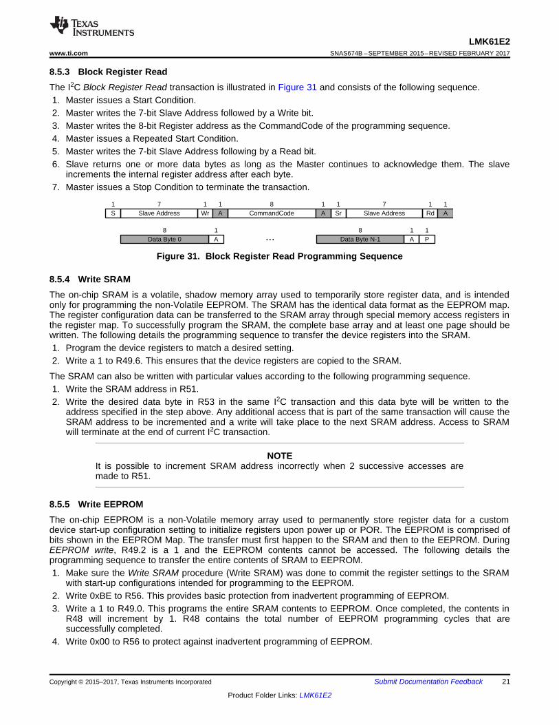
8.5.3 Block Register ReadThe I2C Block Register Read transaction is illustrated in Figure 31 and consists of the following sequence.1. Master issues a Start Condition.2. Master writes the 7-bit Slave Address followed by a Write bit.3. Master writes the 8-bit Register address as the CommandCode of the programming sequence.4. Master issues a Repeated Start Condition.5. Master writes the 7-bit Slave Address following by a Read bit.6. Slave returns one or more data bytes as long as the Master continues to acknowledge them. The slave
increments the internal register address after each byte.7. Master issues a Stop Condition to terminate the transaction.
Figure 31. Block Register Read Programming Sequence
8.5.4 Write SRAMThe on-chip SRAM is a volatile, shadow memory array used to temporarily store register data, and is intendedonly for programming the non-Volatile EEPROM. The SRAM has the identical data format as the EEPROM map.The register configuration data can be transferred to the SRAM array through special memory access registers inthe register map. To successfully program the SRAM, the complete base array and at least one page should bewritten. The following details the programming sequence to transfer the device registers into the SRAM.1. Program the device registers to match a desired setting.2. Write a 1 to R49.6. This ensures that the device registers are copied to the SRAM.
The SRAM can also be written with particular values according to the following programming sequence.1. Write the SRAM address in R51.2. Write the desired data byte in R53 in the same I2C transaction and this data byte will be written to the
address specified in the step above. Any additional access that is part of the same transaction will cause theSRAM address to be incremented and a write will take place to the next SRAM address. Access to SRAMwill terminate at the end of current I2C transaction.
NOTEIt is possible to increment SRAM address incorrectly when 2 successive accesses aremade to R51.
8.5.5 Write EEPROMThe on-chip EEPROM is a non-Volatile memory array used to permanently store register data for a customdevice start-up configuration setting to initialize registers upon power up or POR. The EEPROM is comprised ofbits shown in the EEPROM Map. The transfer must first happen to the SRAM and then to the EEPROM. DuringEEPROM write, R49.2 is a 1 and the EEPROM contents cannot be accessed. The following details theprogramming sequence to transfer the entire contents of SRAM to EEPROM.1. Make sure the Write SRAM procedure (Write SRAM) was done to commit the register settings to the SRAM
with start-up configurations intended for programming to the EEPROM.2. Write 0xBE to R56. This provides basic protection from inadvertent programming of EEPROM.3. Write a 1 to R49.0. This programs the entire SRAM contents to EEPROM. Once completed, the contents in
R48 will increment by 1. R48 contains the total number of EEPROM programming cycles that aresuccessfully completed.
4. Write 0x00 to R56 to protect against inadvertent programming of EEPROM.
22
LMK61E2SNAS674B –SEPTEMBER 2015–REVISED FEBRUARY 2017 www.ti.com
Product Folder Links: LMK61E2
Submit Documentation Feedback Copyright © 2015–2017, Texas Instruments Incorporated
8.5.6 Read SRAMThe contents of the SRAM can be read out, one word at a time, starting with that of the requested address.Following details the programming sequence for an SRAM read by address.1. Write the SRAM address in R51.2. The SRAM data located at the address specified in the step above can be obtained by reading R53 in the
same I2C transaction. Any additional access that is part of the same transaction will cause the SRAMaddress to be incremented and a read will take place of the next SRAM address. Access to SRAM willterminate at the end of current I2C transaction.
NOTEIt is possible to increment SRAM address incorrectly when 2 successive accesses aremade to R51.
8.5.7 Read EEPROMThe contents of the EEPROM can be read out, one word at a time, starting with that of the requested address.Following details the programming sequence for an EEPROM read by address.1. Write the EEPROM address in R51.2. The EEPROM data located at the address specified in the step above can be obtained by reading R52 in the
same I2C transaction. Any additional access that is part of the same transaction will cause the EEPROMaddress to be incremented and a read will take place of the next EEPROM address. Access to EEPROM willterminate at the end of current I2C transaction.
NOTEIt is possible to increment EEPROM address incorrectly when 2 successive accesses aremade to R51.
LMK61E2www.ti.com SNAS674B –SEPTEMBER 2015–REVISED FEBRUARY 2017
23
Product Folder Links: LMK61E2
Submit Documentation FeedbackCopyright © 2015–2017, Texas Instruments Incorporated
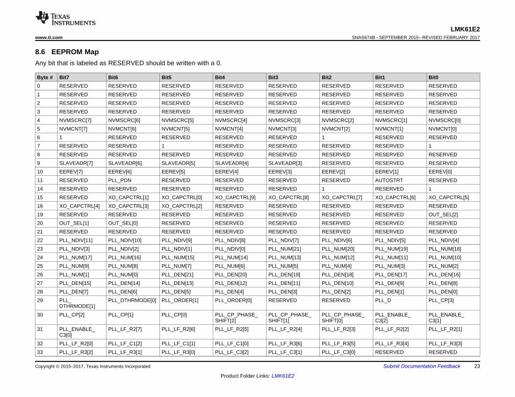
8.6 EEPROM MapAny bit that is labeled as RESERVED should be written with a 0.
Byte # Bit7 Bit6 Bit5 Bit4 Bit3 Bit2 Bit1 Bit00 RESERVED RESERVED RESERVED RESERVED RESERVED RESERVED RESERVED RESERVED1 RESERVED RESERVED RESERVED RESERVED RESERVED RESERVED RESERVED RESERVED2 RESERVED RESERVED RESERVED RESERVED RESERVED RESERVED RESERVED RESERVED3 RESERVED RESERVED RESERVED RESERVED RESERVED RESERVED RESERVED RESERVED4 NVMSCRC[7] NVMSCRC[6] NVMSCRC[5] NVMSCRC[4] NVMSCRC[3] NVMSCRC[2] NVMSCRC[1] NVMSCRC[0]5 NVMCNT[7] NVMCNT[6] NVMCNT[5] NVMCNT[4] NVMCNT[3] NVMCNT[2] NVMCNT[1] NVMCNT[0]6 1 RESERVED RESERVED RESERVED RESERVED 1 RESERVED RESERVED7 RESERVED RESERVED 1 RESERVED RESERVED RESERVED RESERVED 18 RESERVED RESERVED RESERVED RESERVED RESERVED RESERVED RESERVED RESERVED9 SLAVEADR[7] SLAVEADR[6] SLAVEADR[5] SLAVEADR[4] SLAVEADR[3] RESERVED RESERVED RESERVED10 EEREV[7] EEREV[6] EEREV[5] EEREV[4] EEREV[3] EEREV[2] EEREV[1] EEREV[0]11 RESERVED PLL_PDN RESERVED RESERVED RESERVED RESERVED AUTOSTRT RESERVED14 RESERVED RESERVED RESERVED RESERVED RESERVED 1 RESERVED 115 RESERVED XO_CAPCTRL[1] XO_CAPCTRL[0] XO_CAPCTRL[9] XO_CAPCTRL[8] XO_CAPCTRL[7] XO_CAPCTRL[6] XO_CAPCTRL[5]16 XO_CAPCTRL[4] XO_CAPCTRL[3] XO_CAPCTRL[2] RESERVED RESERVED RESERVED RESERVED RESERVED19 RESERVED RESERVED RESERVED RESERVED RESERVED RESERVED RESERVED OUT_SEL[2]20 OUT_SEL[1] OUT_SEL[0] RESERVED RESERVED RESERVED RESERVED RESERVED RESERVED21 RESERVED RESERVED RESERVED RESERVED RESERVED RESERVED RESERVED RESERVED22 PLL_NDIV[11] PLL_NDIV[10] PLL_NDIV[9] PLL_NDIV[8] PLL_NDIV[7] PLL_NDIV[6] PLL_NDIV[5] PLL_NDIV[4]23 PLL_NDIV[3] PLL_NDIV[2] PLL_NDIV[1] PLL_NDIV[0] PLL_NUM[21] PLL_NUM[20] PLL_NUM[19] PLL_NUM[18]24 PLL_NUM[17] PLL_NUM[16] PLL_NUM[15] PLL_NUM[14] PLL_NUM[13] PLL_NUM[12] PLL_NUM[11] PLL_NUM[10]25 PLL_NUM[9] PLL_NUM[8] PLL_NUM[7] PLL_NUM[6] PLL_NUM[5] PLL_NUM[4] PLL_NUM[3] PLL_NUM[2]26 PLL_NUM[1] PLL_NUM[0] PLL_DEN[21] PLL_DEN[20] PLL_DEN[19] PLL_DEN[18] PLL_DEN[17] PLL_DEN[16]27 PLL_DEN[15] PLL_DEN[14] PLL_DEN[13] PLL_DEN[12] PLL_DEN[11] PLL_DEN[10] PLL_DEN[9] PLL_DEN[8]28 PLL_DEN[7] PLL_DEN[6] PLL_DEN[5] PLL_DEN[4] PLL_DEN[3] PLL_DEN[2] PLL_DEN[1] PLL_DEN[0]29 PLL_
DTHRMODE[1]PLL_DTHRMODE[0] PLL_ORDER[1] PLL_ORDER[0] RESERVED RESERVED PLL_D PLL_CP[3]
30 PLL_CP[2] PLL_CP[1] PLL_CP[0] PLL_CP_PHASE_SHIFT[2]
PLL_CP_PHASE_SHIFT[1]
PLL_CP_PHASE_SHIFT[0]
PLL_ENABLE_C3[2]
PLL_ENABLE_C3[1]
31 PLL_ENABLE_C3[0]
PLL_LF_R2[7] PLL_LF_R2[6] PLL_LF_R2[5] PLL_LF_R2[4] PLL_LF_R2[3] PLL_LF_R2[2] PLL_LF_R2[1]
32 PLL_LF_R2[0] PLL_LF_C1[2] PLL_LF_C1[1] PLL_LF_C1[0] PLL_LF_R3[6] PLL_LF_R3[5] PLL_LF_R3[4] PLL_LF_R3[3]33 PLL_LF_R3[2] PLL_LF_R3[1] PLL_LF_R3[0] PLL_LF_C3[2] PLL_LF_C3[1] PLL_LF_C3[0] RESERVED RESERVED
LMK61E2SNAS674B –SEPTEMBER 2015–REVISED FEBRUARY 2017 www.ti.com
24
Product Folder Links: LMK61E2
Submit Documentation Feedback Copyright © 2015–2017, Texas Instruments Incorporated
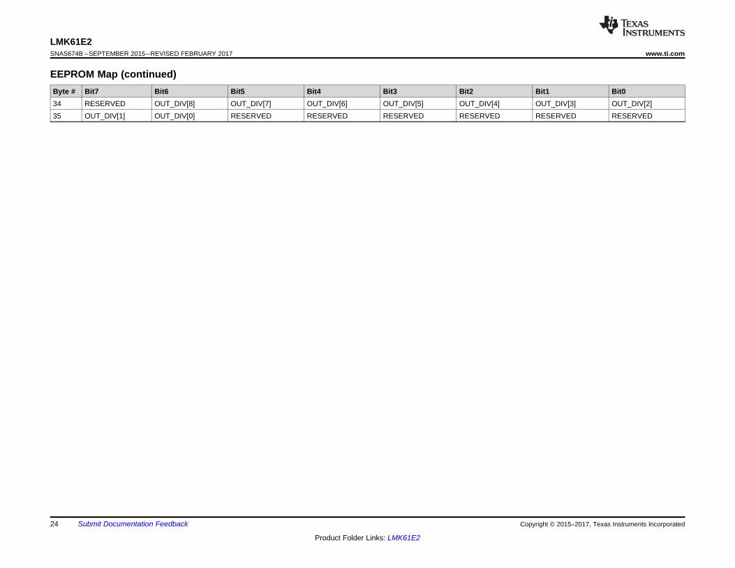
EEPROM Map (continued)Byte # Bit7 Bit6 Bit5 Bit4 Bit3 Bit2 Bit1 Bit034 RESERVED OUT_DIV[8] OUT_DIV[7] OUT_DIV[6] OUT_DIV[5] OUT_DIV[4] OUT_DIV[3] OUT_DIV[2]35 OUT_DIV[1] OUT_DIV[0] RESERVED RESERVED RESERVED RESERVED RESERVED RESERVED
LMK61E2www.ti.com SNAS674B –SEPTEMBER 2015–REVISED FEBRUARY 2017
25
Product Folder Links: LMK61E2
Submit Documentation FeedbackCopyright © 2015–2017, Texas Instruments Incorporated
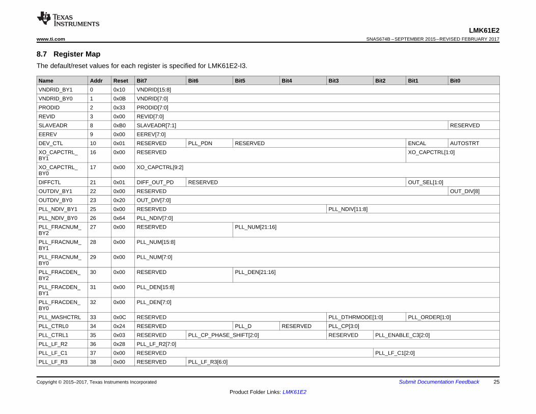
8.7 Register MapThe default/reset values for each register is specified for LMK61E2-I3.
Name Addr Reset Bit7 Bit6 Bit5 Bit4 Bit3 Bit2 Bit1 Bit0VNDRID_BY1 0 0x10 VNDRID[15:8]VNDRID_BY0 1 0x0B VNDRID[7:0]PRODID 2 0x33 PRODID[7:0]REVID 3 0x00 REVID[7:0]SLAVEADR 8 0xB0 SLAVEADR[7:1] RESERVEDEEREV 9 0x00 EEREV[7:0]DEV_CTL 10 0x01 RESERVED PLL_PDN RESERVED ENCAL AUTOSTRTXO_CAPCTRL_BY1
16 0x00 RESERVED XO_CAPCTRL[1:0]
XO_CAPCTRL_BY0
17 0x00 XO_CAPCTRL[9:2]
DIFFCTL 21 0x01 DIFF_OUT_PD RESERVED OUT_SEL[1:0]OUTDIV_BY1 22 0x00 RESERVED OUT_DIV[8]OUTDIV_BY0 23 0x20 OUT_DIV[7:0]PLL_NDIV_BY1 25 0x00 RESERVED PLL_NDIV[11:8]PLL_NDIV_BY0 26 0x64 PLL_NDIV[7:0]PLL_FRACNUM_BY2
27 0x00 RESERVED PLL_NUM[21:16]
PLL_FRACNUM_BY1
28 0x00 PLL_NUM[15:8]
PLL_FRACNUM_BY0
29 0x00 PLL_NUM[7:0]
PLL_FRACDEN_BY2
30 0x00 RESERVED PLL_DEN[21:16]
PLL_FRACDEN_BY1
31 0x00 PLL_DEN[15:8]
PLL_FRACDEN_BY0
32 0x00 PLL_DEN[7:0]
PLL_MASHCTRL 33 0x0C RESERVED PLL_DTHRMODE[1:0] PLL_ORDER[1:0]PLL_CTRL0 34 0x24 RESERVED PLL_D RESERVED PLL_CP[3:0]PLL_CTRL1 35 0x03 RESERVED PLL_CP_PHASE_SHIFT[2:0] RESERVED PLL_ENABLE_C3[2:0]PLL_LF_R2 36 0x28 PLL_LF_R2[7:0]PLL_LF_C1 37 0x00 RESERVED PLL_LF_C1[2:0]PLL_LF_R3 38 0x00 RESERVED PLL_LF_R3[6:0]
LMK61E2SNAS674B –SEPTEMBER 2015–REVISED FEBRUARY 2017 www.ti.com
26
Product Folder Links: LMK61E2
Submit Documentation Feedback Copyright © 2015–2017, Texas Instruments Incorporated
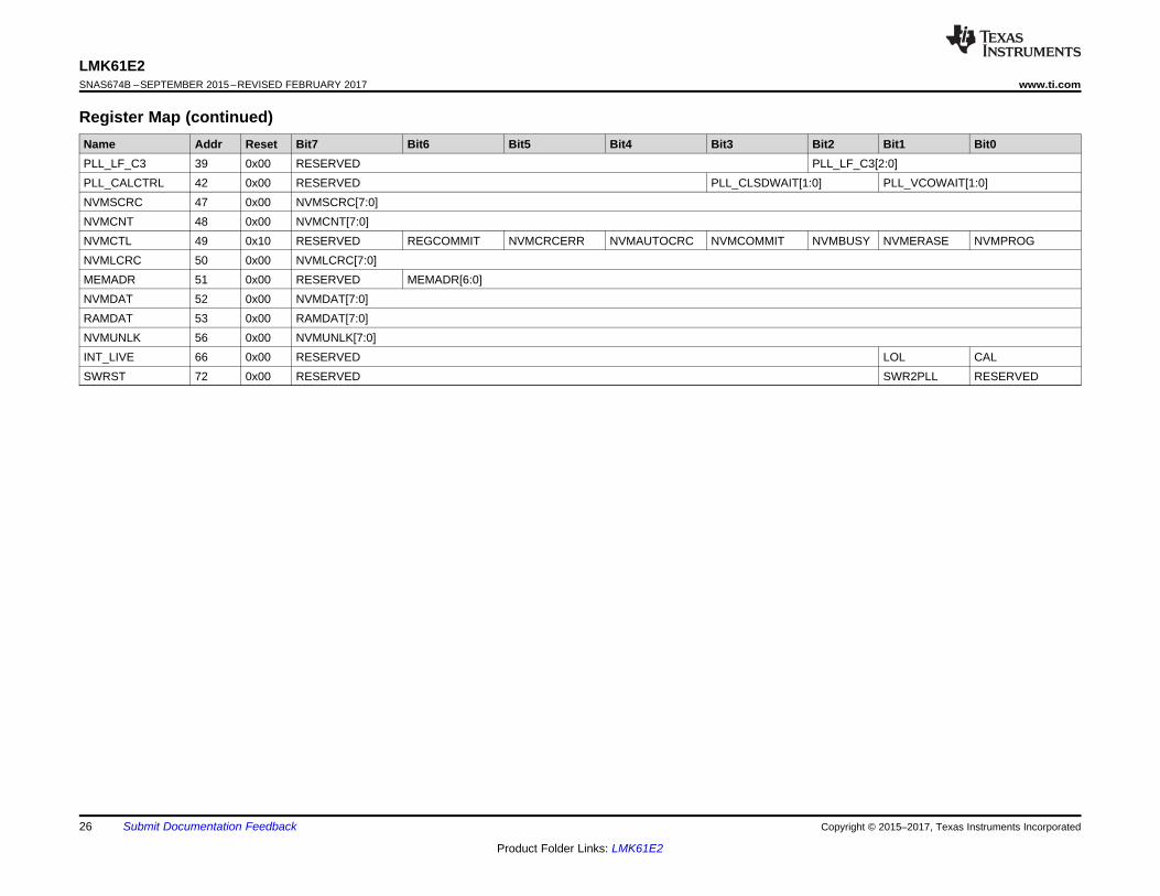
Register Map (continued)Name Addr Reset Bit7 Bit6 Bit5 Bit4 Bit3 Bit2 Bit1 Bit0PLL_LF_C3 39 0x00 RESERVED PLL_LF_C3[2:0]PLL_CALCTRL 42 0x00 RESERVED PLL_CLSDWAIT[1:0] PLL_VCOWAIT[1:0]NVMSCRC 47 0x00 NVMSCRC[7:0]NVMCNT 48 0x00 NVMCNT[7:0]NVMCTL 49 0x10 RESERVED REGCOMMIT NVMCRCERR NVMAUTOCRC NVMCOMMIT NVMBUSY NVMERASE NVMPROGNVMLCRC 50 0x00 NVMLCRC[7:0]MEMADR 51 0x00 RESERVED MEMADR[6:0]NVMDAT 52 0x00 NVMDAT[7:0]RAMDAT 53 0x00 RAMDAT[7:0]NVMUNLK 56 0x00 NVMUNLK[7:0]INT_LIVE 66 0x00 RESERVED LOL CALSWRST 72 0x00 RESERVED SWR2PLL RESERVED
27
LMK61E2www.ti.com SNAS674B –SEPTEMBER 2015–REVISED FEBRUARY 2017
Product Folder Links: LMK61E2
Submit Documentation FeedbackCopyright © 2015–2017, Texas Instruments Incorporated
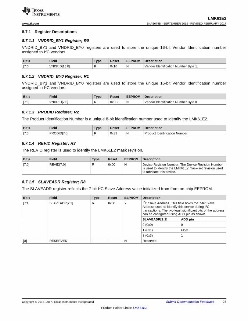
8.7.1 Register Descriptions
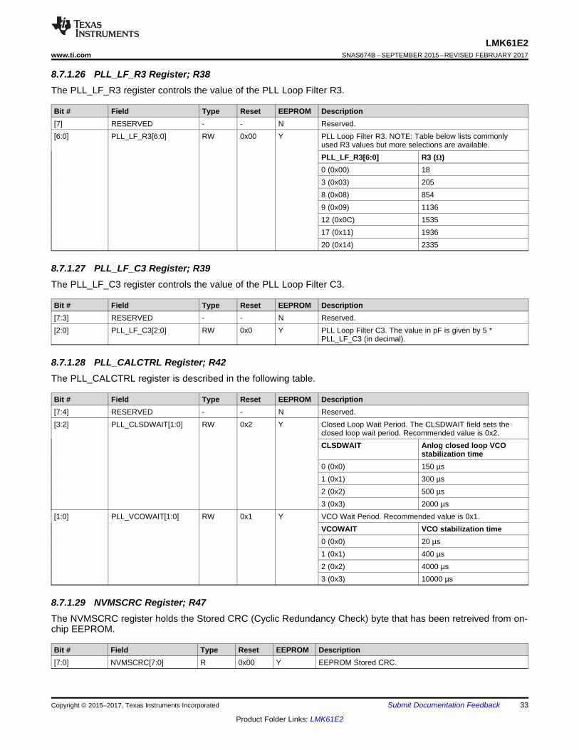
8.7.1.1 VNDRID_BY1 Register; R0VNDRID_BY1 and VNDRID_BY0 registers are used to store the unique 16-bit Vendor Identification numberassigned to I2C vendors.
Bit # Field Type Reset EEPROM Description[7:0] VNDRID[15:8] R 0x10 N Vendor Identification Number Byte 1.
8.7.1.2 VNDRID_BY0 Register; R1VNDRID_BY1 and VNDRID_BY0 registers are used to store the unique 16-bit Vendor Identification numberassigned to I2C vendors.
Bit # Field Type Reset EEPROM Description[7:0] VNDRID[7:0] R 0x0B N Vendor Identification Number Byte 0.
8.7.1.3 PRODID Register; R2The Product Identification Number is a unique 8-bit identification number used to identify the LMK61E2.
Bit # Field Type Reset EEPROM Description[7:0] PRODID[7:0] R 0x33 N Product Identification Number.
8.7.1.4 REVID Register; R3The REVID register is used to identify the LMK61E2 mask revision.
Bit # Field Type Reset EEPROM Description[7:0] REVID[7:0] R 0x00 N Device Revision Number. The Device Revision Number
is used to identify the LMK61E2 mask-set revision usedto fabricate this device.
8.7.1.5 SLAVEADR Register; R8The SLAVEADR register reflects the 7-bit I2C Slave Address value initialized from from on-chip EEPROM.
Bit # Field Type Reset EEPROM Description[7:1] SLAVEADR[7:1] R 0x58 Y I2C Slave Address. This field holds the 7-bit Slave
Address used to identify this device during I2Ctransactions. The two least significant bits of the addresscan be configured using ADD pin as shown.SLAVEADR[2:1] ADD pin0 (0x0) 01 (0x1) Float3 (0x3) 1
[0] RESERVED - - N Reserved.
28
LMK61E2SNAS674B –SEPTEMBER 2015–REVISED FEBRUARY 2017 www.ti.com
Product Folder Links: LMK61E2
Submit Documentation Feedback Copyright © 2015–2017, Texas Instruments Incorporated
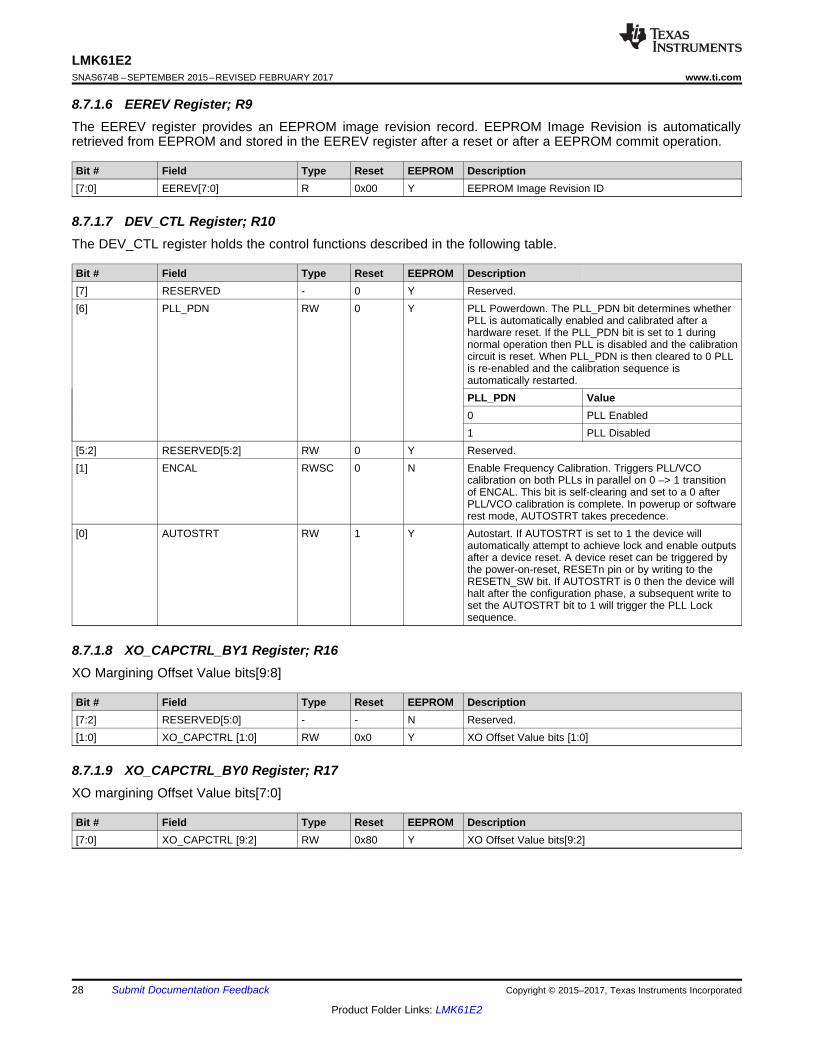
8.7.1.6 EEREV Register; R9The EEREV register provides an EEPROM image revision record. EEPROM Image Revision is automaticallyretrieved from EEPROM and stored in the EEREV register after a reset or after a EEPROM commit operation.
Bit # Field Type Reset EEPROM Description[7:0] EEREV[7:0] R 0x00 Y EEPROM Image Revision ID
8.7.1.7 DEV_CTL Register; R10The DEV_CTL register holds the control functions described in the following table.
Bit # Field Type Reset EEPROM Description[7] RESERVED - 0 Y Reserved.[6] PLL_PDN RW 0 Y PLL Powerdown. The PLL_PDN bit determines whether
PLL is automatically enabled and calibrated after ahardware reset. If the PLL_PDN bit is set to 1 duringnormal operation then PLL is disabled and the calibrationcircuit is reset. When PLL_PDN is then cleared to 0 PLLis re-enabled and the calibration sequence isautomatically restarted.PLL_PDN Value0 PLL Enabled1 PLL Disabled
[5:2] RESERVED[5:2] RW 0 Y Reserved.[1] ENCAL RWSC 0 N Enable Frequency Calibration. Triggers PLL/VCO
calibration on both PLLs in parallel on 0 –> 1 transitionof ENCAL. This bit is self-clearing and set to a 0 afterPLL/VCO calibration is complete. In powerup or softwarerest mode, AUTOSTRT takes precedence.
[0] AUTOSTRT RW 1 Y Autostart. If AUTOSTRT is set to 1 the device willautomatically attempt to achieve lock and enable outputsafter a device reset. A device reset can be triggered bythe power-on-reset, RESETn pin or by writing to theRESETN_SW bit. If AUTOSTRT is 0 then the device willhalt after the configuration phase, a subsequent write toset the AUTOSTRT bit to 1 will trigger the PLL Locksequence.
8.7.1.8 XO_CAPCTRL_BY1 Register; R16XO Margining Offset Value bits[9:8]
Bit # Field Type Reset EEPROM Description[7:2] RESERVED[5:0] - - N Reserved.[1:0] XO_CAPCTRL [1:0] RW 0x0 Y XO Offset Value bits [1:0]
8.7.1.9 XO_CAPCTRL_BY0 Register; R17XO margining Offset Value bits[7:0]
Bit # Field Type Reset EEPROM Description[7:0] XO_CAPCTRL [9:2] RW 0x80 Y XO Offset Value bits[9:2]
29
LMK61E2www.ti.com SNAS674B –SEPTEMBER 2015–REVISED FEBRUARY 2017
Product Folder Links: LMK61E2
Submit Documentation FeedbackCopyright © 2015–2017, Texas Instruments Incorporated
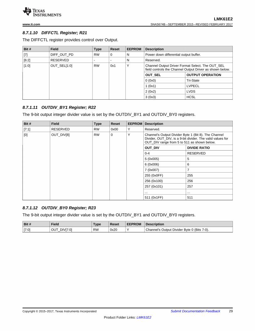
8.7.1.10 DIFFCTL Register; R21The DIFFCTL register provides control over Output.
Bit # Field Type Reset EEPROM Description[7] DIFF_OUT_PD RW 0 N Power down differential output buffer.[6:2] RESERVED - - N Reserved.[1:0] OUT_SEL[1:0] RW 0x1 Y Channel Output Driver Format Select. The OUT_SEL
field controls the Channel Output Driver as shown below.OUT_SEL OUTPUT OPERATION0 (0x0) Tri-State1 (0x1) LVPECL2 (0x2) LVDS3 (0x3) HCSL
8.7.1.11 OUTDIV_BY1 Register; R22The 9-bit output integer divider value is set by the OUTDIV_BY1 and OUTDIV_BY0 registers.
Bit # Field Type Reset EEPROM Description[7:1] RESERVED RW 0x00 Y Reserved.[0] OUT_DIV[8] RW 0 Y Channel's Output Divider Byte 1 (Bit 8). The Channel
Divider, OUT_DIV, is a 9-bit divider. The valid values forOUT_DIV range from 5 to 511 as shown below.OUT_DIV DIVIDE RATIO0-4 RESERVED5 (0x005) 56 (0x006) 67 (0x007) 7255 (0x0FF) 255256 (0x100) 256257 (0x101) 257... ...511 (0x1FF) 511
8.7.1.12 OUTDIV_BY0 Register; R23The 9-bit output integer divider value is set by the OUTDIV_BY1 and OUTDIV_BY0 registers.
Bit # Field Type Reset EEPROM Description[7:0] OUT_DIV[7:0] RW 0x20 Y Channel's Output Divider Byte 0 (Bits 7-0).
30
LMK61E2SNAS674B –SEPTEMBER 2015–REVISED FEBRUARY 2017 www.ti.com
Product Folder Links: LMK61E2
Submit Documentation Feedback Copyright © 2015–2017, Texas Instruments Incorporated
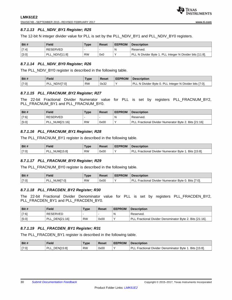
8.7.1.13 PLL_NDIV_BY1 Register; R25The 12-bit N integer divider value for PLL is set by the PLL_NDIV_BY1 and PLL_NDIV_BY0 registers.
Bit # Field Type Reset EEPROM Description[7:4] RESERVED - - N Reserved.[3:0] PLL_NDIV[11:8] RW 0x0 Y PLL N Divider Byte 1. PLL Integer N Divider bits [11:8].
8.7.1.14 PLL_NDIV_BY0 Register; R26The PLL_NDIV_BY0 register is described in the following table.
Bit # Field Type Reset EEPROM Description[7:0] PLL_NDIV[7:0] RW 0x32 Y PLL N Divider Byte 0. PLL Integer N Divider bits [7:0].
8.7.1.15 PLL_FRACNUM_BY2 Register; R27The 22-bit Fractional Divider Numerator value for PLL is set by registers PLL_FRACNUM_BY2,PLL_FRACNUM_BY1 and PLL_FRACNUM_BY0.
Bit # Field Type Reset EEPROM Description[7:6] RESERVED - - N Reserved.[5:0] PLL_NUM[21:16] RW 0x00 Y PLL Fractional Divider Numerator Byte 2. Bits [21:16]
8.7.1.16 PLL_FRACNUM_BY1 Register; R28The PLL_FRACNUM_BY1 register is described in the following table.
Bit # Field Type Reset EEPROM Description[7:0] PLL_NUM[15:8] RW 0x00 Y PLL Fractional Divider Numerator Byte 1. Bits [15:8].
8.7.1.17 PLL_FRACNUM_BY0 Register; R29The PLL_FRACNUM_BY0 register is described in the following table.
Bit # Field Type Reset EEPROM Description[7:0] PLL_NUM[7:0] RW 0x00 Y PLL Fractional Divider Numerator Byte 0. Bits [7:0].
8.7.1.18 PLL_FRACDEN_BY2 Register; R30The 22-bit Fractional Divider Denominator value for PLL is set by registers PLL_FRACDEN_BY2,PLL_FRACDEN_BY1 and PLL_FRACDEN_BY0.
Bit # Field Type Reset EEPROM Description[7:6] RESERVED - - N Reserved.[5:0] PLL_DEN[21:16] RW 0x00 Y PLL Fractional Divider Denominator Byte 2. Bits [21:16].
8.7.1.19 PLL_FRACDEN_BY1 Register; R31The PLL_FRACDEN_BY1 register is described in the following table.
Bit # Field Type Reset EEPROM Description[7:0] PLL_DEN[15:8] RW 0x00 Y PLL Fractional Divider Denominator Byte 1. Bits [15:8].
31
LMK61E2www.ti.com SNAS674B –SEPTEMBER 2015–REVISED FEBRUARY 2017
Product Folder Links: LMK61E2
Submit Documentation FeedbackCopyright © 2015–2017, Texas Instruments Incorporated
8.7.1.20 PLL_FRACDEN_BY0 Register; R32The PLL_FRACDEN_BY0 register is described in the following table.
Bit # Field Type Reset EEPROM Description[7:0] PLL_DEN[7:0] RW 0x00 Y PLL Fractional Divider Denominator Byte 0. Bits [7:0].
8.7.1.21 PLL_MASHCTRL Register; R33The PLL_MASHCTRL register provides control of the fractional divider for PLL.
Bit # Field Type Reset EEPROM Description[7:4] RESERVED - - N Reserved.[3:2] PLL_DTHRMODE[1:0] RW 0x3 Y Mash Engine dither mode control.
DITHERMODE Dither Configuration0 (0x0) Weak1 (0x1) Reserved2 (0x2) Reserved3 (0x3) Dither Disabled
[1:0] PLL_ORDER[1:0] RW 0x0 Y Mash Engine Order.ORDER Order Configuration0 (0x0) Integer Mode Divider1 (0x1) Reserved2 (0x2) Reserved3 (0x3) 3rd order
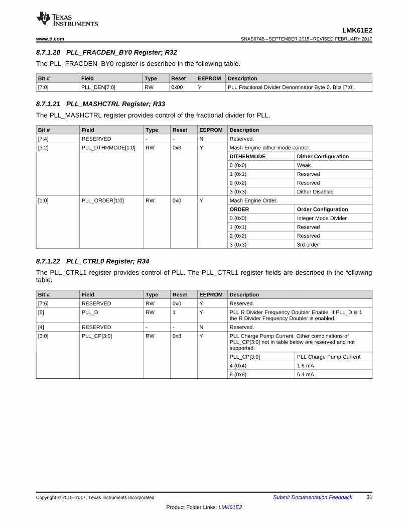
8.7.1.22 PLL_CTRL0 Register; R34The PLL_CTRL1 register provides control of PLL. The PLL_CTRL1 register fields are described in the followingtable.
Bit # Field Type Reset EEPROM Description[7:6] RESERVED RW 0x0 Y Reserved.[5] PLL_D RW 1 Y PLL R Divider Frequency Doubler Enable. If PLL_D is 1
the R Divider Frequency Doubler is enabled.[4] RESERVED - - N Reserved.[3:0] PLL_CP[3:0] RW 0x8 Y PLL Charge Pump Current. Other combinations of
PLL_CP[3:0] not in table below are reserved and notsupported.PLL_CP[3:0] PLL Charge Pump Current4 (0x4) 1.6 mA8 (0x8) 6.4 mA
32
LMK61E2SNAS674B –SEPTEMBER 2015–REVISED FEBRUARY 2017 www.ti.com
Product Folder Links: LMK61E2
Submit Documentation Feedback Copyright © 2015–2017, Texas Instruments Incorporated
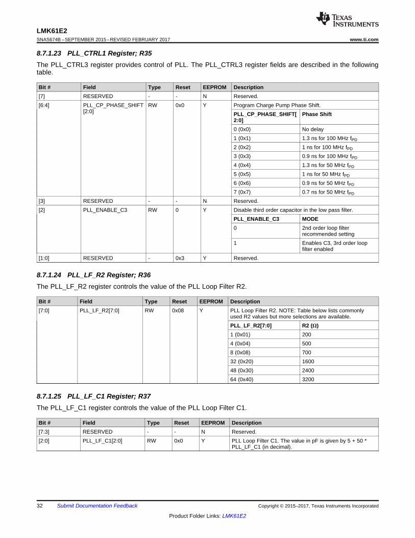
8.7.1.23 PLL_CTRL1 Register; R35The PLL_CTRL3 register provides control of PLL. The PLL_CTRL3 register fields are described in the followingtable.
Bit # Field Type Reset EEPROM Description[7] RESERVED - - N Reserved.[6:4] PLL_CP_PHASE_SHIFT
[2:0]RW 0x0 Y Program Charge Pump Phase Shift.
PLL_CP_PHASE_SHIFT[2:0]
Phase Shift
0 (0x0) No delay1 (0x1) 1.3 ns for 100 MHz fPD
2 (0x2) 1 ns for 100 MHz fPD
3 (0x3) 0.9 ns for 100 MHz fPD
4 (0x4) 1.3 ns for 50 MHz fPD
5 (0x5) 1 ns for 50 MHz fPD
6 (0x6) 0.9 ns for 50 MHz fPD
7 (0x7) 0.7 ns for 50 MHz fPD
[3] RESERVED - - N Reserved.[2] PLL_ENABLE_C3 RW 0 Y Disable third order capacitor in the low pass filter.
PLL_ENABLE_C3 MODE0 2nd order loop filter
recommended setting1 Enables C3, 3rd order loop
filter enabled[1:0] RESERVED - 0x3 Y Reserved.
8.7.1.24 PLL_LF_R2 Register; R36The PLL_LF_R2 register controls the value of the PLL Loop Filter R2.
Bit # Field Type Reset EEPROM Description[7:0] PLL_LF_R2[7:0] RW 0x08 Y PLL Loop Filter R2. NOTE: Table below lists commonly
used R2 values but more selections are available.PLL_LF_R2[7:0] R2 (Ω)1 (0x01) 2004 (0x04) 5008 (0x08) 70032 (0x20) 160048 (0x30) 240064 (0x40) 3200
8.7.1.25 PLL_LF_C1 Register; R37The PLL_LF_C1 register controls the value of the PLL Loop Filter C1.
Bit # Field Type Reset EEPROM Description[7:3] RESERVED - - N Reserved.[2:0] PLL_LF_C1[2:0] RW 0x0 Y PLL Loop Filter C1. The value in pF is given by 5 + 50 *
PLL_LF_C1 (in decimal).
33
LMK61E2www.ti.com SNAS674B –SEPTEMBER 2015–REVISED FEBRUARY 2017
Product Folder Links: LMK61E2
Submit Documentation FeedbackCopyright © 2015–2017, Texas Instruments Incorporated
8.7.1.26 PLL_LF_R3 Register; R38The PLL_LF_R3 register controls the value of the PLL Loop Filter R3.
Bit # Field Type Reset EEPROM Description[7] RESERVED - - N Reserved.[6:0] PLL_LF_R3[6:0] RW 0x00 Y PLL Loop Filter R3. NOTE: Table below lists commonly
used R3 values but more selections are available.PLL_LF_R3[6:0] R3 (Ω)0 (0x00) 183 (0x03) 2058 (0x08) 8549 (0x09) 113612 (0x0C) 153517 (0x11) 193620 (0x14) 2335
8.7.1.27 PLL_LF_C3 Register; R39The PLL_LF_C3 register controls the value of the PLL Loop Filter C3.
Bit # Field Type Reset EEPROM Description[7:3] RESERVED - - N Reserved.[2:0] PLL_LF_C3[2:0] RW 0x0 Y PLL Loop Filter C3. The value in pF is given by 5 *
PLL_LF_C3 (in decimal).
8.7.1.28 PLL_CALCTRL Register; R42The PLL_CALCTRL register is described in the following table.
Bit # Field Type Reset EEPROM Description[7:4] RESERVED - - N Reserved.[3:2] PLL_CLSDWAIT[1:0] RW 0x2 Y Closed Loop Wait Period. The CLSDWAIT field sets the
closed loop wait period. Recommended value is 0x2.CLSDWAIT Anlog closed loop VCO
stabilization time0 (0x0) 150 µs1 (0x1) 300 µs2 (0x2) 500 µs3 (0x3) 2000 µs
[1:0] PLL_VCOWAIT[1:0] RW 0x1 Y VCO Wait Period. Recommended value is 0x1.VCOWAIT VCO stabilization time0 (0x0) 20 µs1 (0x1) 400 µs2 (0x2) 4000 µs3 (0x3) 10000 µs
8.7.1.29 NVMSCRC Register; R47The NVMSCRC register holds the Stored CRC (Cyclic Redundancy Check) byte that has been retreived from on-chip EEPROM.
Bit # Field Type Reset EEPROM Description[7:0] NVMSCRC[7:0] R 0x00 Y EEPROM Stored CRC.
34
LMK61E2SNAS674B –SEPTEMBER 2015–REVISED FEBRUARY 2017 www.ti.com
Product Folder Links: LMK61E2
Submit Documentation Feedback Copyright © 2015–2017, Texas Instruments Incorporated
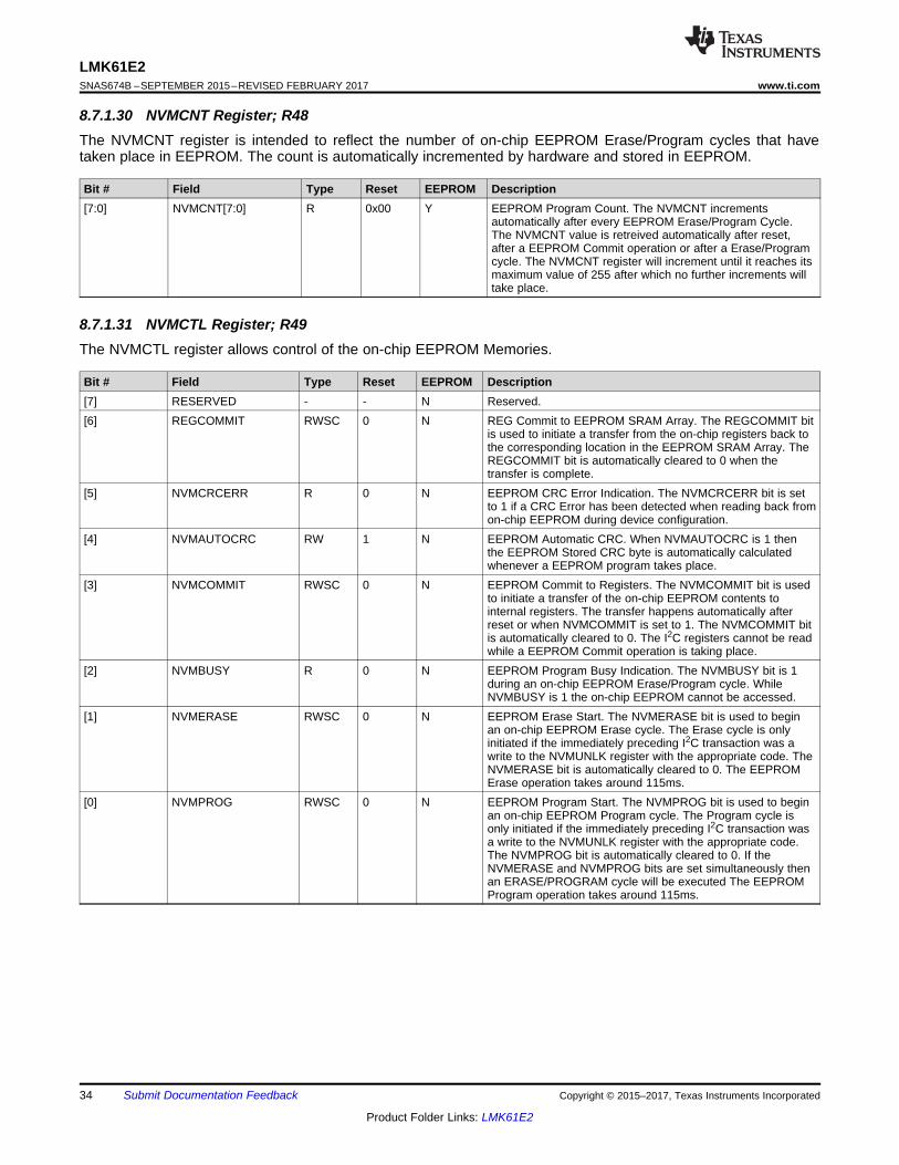
8.7.1.30 NVMCNT Register; R48The NVMCNT register is intended to reflect the number of on-chip EEPROM Erase/Program cycles that havetaken place in EEPROM. The count is automatically incremented by hardware and stored in EEPROM.
Bit # Field Type Reset EEPROM Description[7:0] NVMCNT[7:0] R 0x00 Y EEPROM Program Count. The NVMCNT increments
automatically after every EEPROM Erase/Program Cycle.The NVMCNT value is retreived automatically after reset,after a EEPROM Commit operation or after a Erase/Programcycle. The NVMCNT register will increment until it reaches itsmaximum value of 255 after which no further increments willtake place.
8.7.1.31 NVMCTL Register; R49The NVMCTL register allows control of the on-chip EEPROM Memories.
Bit # Field Type Reset EEPROM Description[7] RESERVED - - N Reserved.[6] REGCOMMIT RWSC 0 N REG Commit to EEPROM SRAM Array. The REGCOMMIT bit
is used to initiate a transfer from the on-chip registers back tothe corresponding location in the EEPROM SRAM Array. TheREGCOMMIT bit is automatically cleared to 0 when thetransfer is complete.
[5] NVMCRCERR R 0 N EEPROM CRC Error Indication. The NVMCRCERR bit is setto 1 if a CRC Error has been detected when reading back fromon-chip EEPROM during device configuration.
[4] NVMAUTOCRC RW 1 N EEPROM Automatic CRC. When NVMAUTOCRC is 1 thenthe EEPROM Stored CRC byte is automatically calculatedwhenever a EEPROM program takes place.
[3] NVMCOMMIT RWSC 0 N EEPROM Commit to Registers. The NVMCOMMIT bit is usedto initiate a transfer of the on-chip EEPROM contents tointernal registers. The transfer happens automatically afterreset or when NVMCOMMIT is set to 1. The NVMCOMMIT bitis automatically cleared to 0. The I2C registers cannot be readwhile a EEPROM Commit operation is taking place.
[2] NVMBUSY R 0 N EEPROM Program Busy Indication. The NVMBUSY bit is 1during an on-chip EEPROM Erase/Program cycle. WhileNVMBUSY is 1 the on-chip EEPROM cannot be accessed.
[1] NVMERASE RWSC 0 N EEPROM Erase Start. The NVMERASE bit is used to beginan on-chip EEPROM Erase cycle. The Erase cycle is onlyinitiated if the immediately preceding I2C transaction was awrite to the NVMUNLK register with the appropriate code. TheNVMERASE bit is automatically cleared to 0. The EEPROMErase operation takes around 115ms.
[0] NVMPROG RWSC 0 N EEPROM Program Start. The NVMPROG bit is used to beginan on-chip EEPROM Program cycle. The Program cycle isonly initiated if the immediately preceding I2C transaction wasa write to the NVMUNLK register with the appropriate code.The NVMPROG bit is automatically cleared to 0. If theNVMERASE and NVMPROG bits are set simultaneously thenan ERASE/PROGRAM cycle will be executed The EEPROMProgram operation takes around 115ms.
35
LMK61E2www.ti.com SNAS674B –SEPTEMBER 2015–REVISED FEBRUARY 2017
Product Folder Links: LMK61E2
Submit Documentation FeedbackCopyright © 2015–2017, Texas Instruments Incorporated
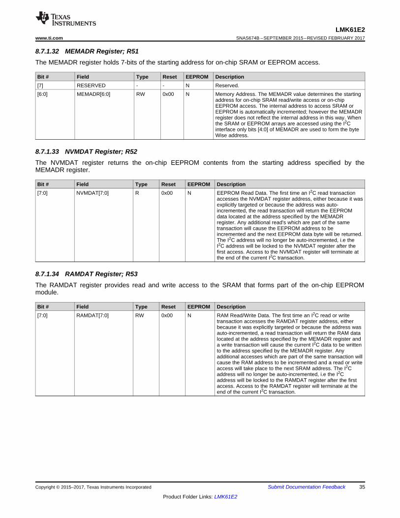
8.7.1.32 MEMADR Register; R51The MEMADR register holds 7-bits of the starting address for on-chip SRAM or EEPROM access.
Bit # Field Type Reset EEPROM Description[7] RESERVED - - N Reserved.[6:0] MEMADR[6:0] RW 0x00 N Memory Address. The MEMADR value determines the starting
address for on-chip SRAM read/write access or on-chipEEPROM access. The internal address to access SRAM orEEPROM is automatically incremented; however the MEMADRregister does not reflect the internal address in this way. Whenthe SRAM or EEPROM arrays are accessed using the I2Cinterface only bits [4:0] of MEMADR are used to form the byteWise address.
8.7.1.33 NVMDAT Register; R52The NVMDAT register returns the on-chip EEPROM contents from the starting address specified by theMEMADR register.
Bit # Field Type Reset EEPROM Description[7:0] NVMDAT[7:0] R 0x00 N EEPROM Read Data. The first time an I2C read transaction
accesses the NVMDAT register address, either because it wasexplicitly targeted or because the address was auto-incremented, the read transaction will return the EEPROMdata located at the address specified by the MEMADRregister. Any additional read's which are part of the sametransaction will cause the EEPROM address to beincremented and the next EEPROM data byte will be returned.The I2C address will no longer be auto-incremented, i.e theI2C address will be locked to the NVMDAT register after thefirst access. Access to the NVMDAT register will terminate atthe end of the current I2C transaction.
8.7.1.34 RAMDAT Register; R53The RAMDAT register provides read and write access to the SRAM that forms part of the on-chip EEPROMmodule.
Bit # Field Type Reset EEPROM Description[7:0] RAMDAT[7:0] RW 0x00 N RAM Read/Write Data. The first time an I2C read or write
transaction accesses the RAMDAT register address, eitherbecause it was explicitly targeted or because the address wasauto-incremented, a read transaction will return the RAM datalocated at the address specified by the MEMADR register anda write transaction will cause the current I2C data to be writtento the address specified by the MEMADR register. Anyadditional accesses which are part of the same transaction willcause the RAM address to be incremented and a read or writeaccess will take place to the next SRAM address. The I2Caddress will no longer be auto-incremented, i.e the I2Caddress will be locked to the RAMDAT register after the firstaccess. Access to the RAMDAT register will terminate at theend of the current I2C transaction.
36
LMK61E2SNAS674B –SEPTEMBER 2015–REVISED FEBRUARY 2017 www.ti.com
Product Folder Links: LMK61E2
Submit Documentation Feedback Copyright © 2015–2017, Texas Instruments Incorporated
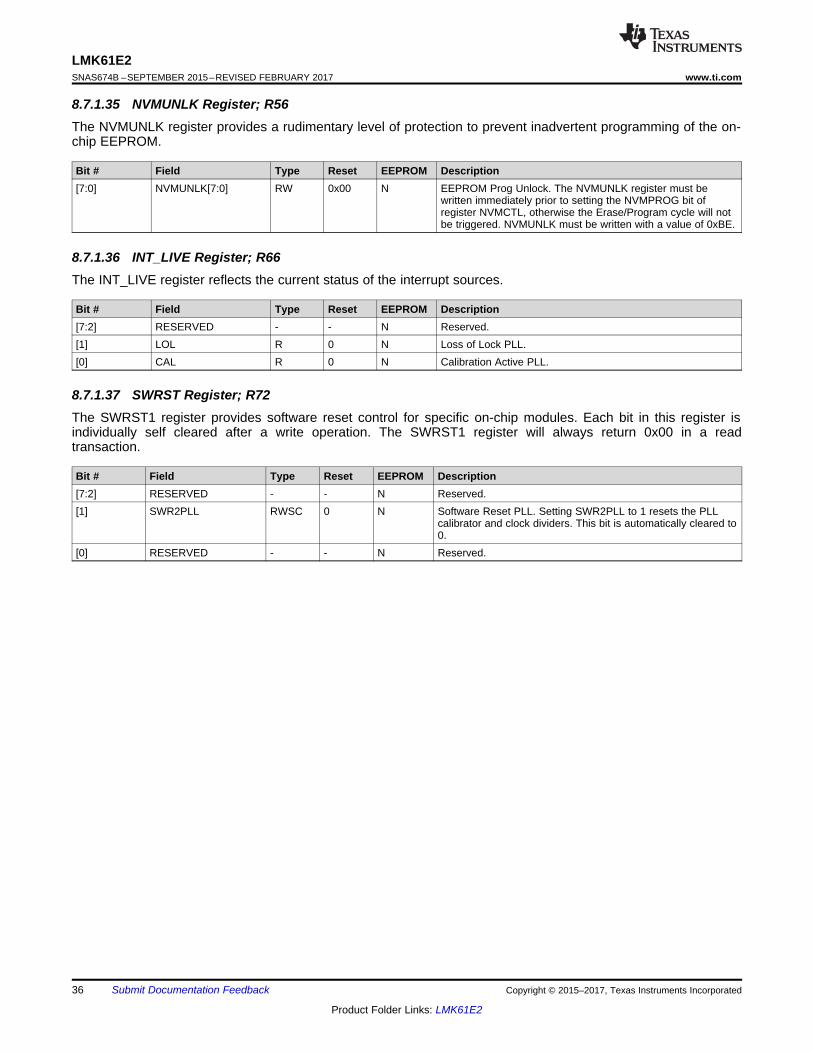
8.7.1.35 NVMUNLK Register; R56The NVMUNLK register provides a rudimentary level of protection to prevent inadvertent programming of the on-chip EEPROM.
Bit # Field Type Reset EEPROM Description[7:0] NVMUNLK[7:0] RW 0x00 N EEPROM Prog Unlock. The NVMUNLK register must be
written immediately prior to setting the NVMPROG bit ofregister NVMCTL, otherwise the Erase/Program cycle will notbe triggered. NVMUNLK must be written with a value of 0xBE.
8.7.1.36 INT_LIVE Register; R66The INT_LIVE register reflects the current status of the interrupt sources.
Bit # Field Type Reset EEPROM Description[7:2] RESERVED - - N Reserved.[1] LOL R 0 N Loss of Lock PLL.[0] CAL R 0 N Calibration Active PLL.
8.7.1.37 SWRST Register; R72The SWRST1 register provides software reset control for specific on-chip modules. Each bit in this register isindividually self cleared after a write operation. The SWRST1 register will always return 0x00 in a readtransaction.
Bit # Field Type Reset EEPROM Description[7:2] RESERVED - - N Reserved.[1] SWR2PLL RWSC 0 N Software Reset PLL. Setting SWR2PLL to 1 resets the PLL
calibrator and clock dividers. This bit is automatically cleared to0.
[0] RESERVED - - N Reserved.
37
LMK61E2www.ti.com SNAS674B –SEPTEMBER 2015–REVISED FEBRUARY 2017
Product Folder Links: LMK61E2
Submit Documentation FeedbackCopyright © 2015–2017, Texas Instruments Incorporated
9 Application and Implementation
NOTEInformation in the following applications sections is not part of the TI componentspecification, and TI does not warrant its accuracy or completeness. TI’s customers areresponsible for determining suitability of components for their purposes. Customers shouldvalidate and test their design implementation to confirm system functionality.
9.1 Application InformationThe LMK61E2 is an ultra-low jitter programmable oscillator that can be used to provide reference clocks for high-speed serial links resulting in improved system performance. The LMK61E2 also supports a variety of featuresthat aids the hardware designer during the system debug and validation phase.
9.2 Typical Applications
9.2.1 Jitter Considerations in Serdes SystemsJitter-sensitive applications such as 10-Gbps or 100-Gbps Ethernet, deploy a serial link using a Serializer in thetransmit section (TX) and a De-serializer in the receive section (RX). These SERDES blocks are typicallyembedded in an ASIC or FPGA. Estimating the clock jitter impact on the link budget requires understanding ofthe TX PLL bandwidth and the RX CDR bandwidth.
As can be seen in Figure 32, the pass band region between the TX low-pass cutoff and RX high-pass cutofffrequencies is the range over which the reference clock jitter adds without any attenuation to the jitter budget ofthe link. Outside of these frequencies, the SERDES link will attenuate the reference clock jitter with a 20 dB/decor even steeper roll-off. Modern ASIC or FPGA designs have some flexibility on deciding the optimal RX CDRbandwidth and TX PLL bandwidth. These bandwidths are typically set based on what is achievable in the ASICor FPGA process node, without increasing design complexity, and on any jitter tolerance or wander specificationthat needs to be met, as related to the RX CDR bandwidth.
The overall allowable jitter in a serial link is dictated by IEEE or other relevant standards. For example,IEEE802.3ba states that the maximum transmit jitter (peak-peak) for 10-Gbps Ethernet should be no more than0.28 × UI and this equates to a 27.1516 ps, p-p for the overall allowable transmit jitter.
The jitter contributing elements are made up of the reference clock, generated potentially from a device likeLMK61E2, the transmit medium, transmit driver, and so forth. Only a portion of the overall allowable transmit jitteris allocated to the reference clock, typically 20% or lower. Therefore, the allowable reference clock jitter, for a20% clock jitter budget, is 5.43 ps, p-p.
Jitter in a reference clock is made up of deterministic jitter (arising from spurious signals due to supply noise ormixing from other outputs or from the reference input) and random jitter (usually due to thermal noise and otheruncorrelated noise sources). A typical clock tree in a serial link system consists of clock generators and fanoutbuffers. The allowable reference clock jitter of 5.43 ps, p-p is needed at the output of the fanout buffer. Modernfanout buffers have low-additive random jitter (less than 100 fs RMS) with no substantial contribution to thedeterministic jitter. Therefore, the clock generator and fanout buffer contribute to the random jitter while theprimary contributor to the deterministic jitter is the clock generator. Rule of thumb, for modern clock generators, isto allocate 25% of allowable reference clock jitter to the deterministic jitter and 75% to the random jitter. Thisamounts to an allowable deterministic jitter of 1.36 ps, p-p and an allowable random jitter of 4.07 ps, p-p. Forserial link systems that need to meet a bit error rate (BER) of 10–12, the allowable random jitter in root-mean-square is 0.29 ps RMS. This is calculated by dividing the p-p jitter by 14 for a BER of 10–12. Accounting forrandom jitter from the fanout buffer, the random jitter needed from the clock generator is 0.27 ps RMS. This iscalculated by the root-mean-square subtraction from the desired jitter at the fanout buffer's output assuming 100fs RMS of additive jitter from the fanout buffer.
With careful frequency planning techniques, like spur optimization (covered in Spur Mitigation Techniques ) andon-chip LDOs to suppress supply noise, the LMK61E2 is able to generate clock outputs with deterministic jitterthat is below 1 ps, p-p and random jitter that is below 0.2 ps RMS. This gives the serial link system withadditional margin on the allowable transmit jitter resulting in a BER better than 10–12.
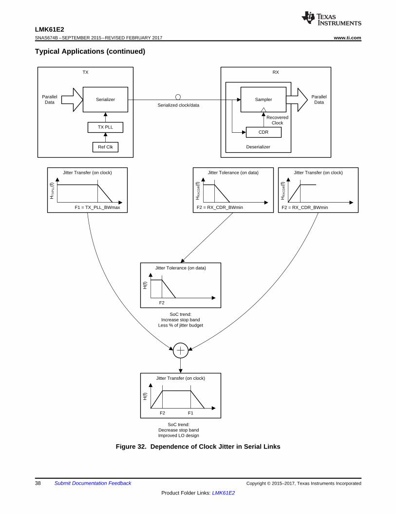
RX
Deserializer
TX
Serializer
TX PLL
Ref Clk
Parallel Data
Jitter Transfer (on clock)
F1 = TX_PLL_BWmax
HT
XP
LL(f
)
Sampler
CDR
Parallel Data
Recovered Clock
Serialized clock/data
Jitter Tolerance (on data)
F2 = RX_CDR_BWmin
HR
XC
DR(f
)
Jitter Transfer (on clock)
F2 = RX_CDR_BWmin
HR
XC
DR(f
)
Jitter Tolerance (on data)
H(f
)
F2
SoC trend: Increase stop band
Less % of jitter budget
Jitter Transfer (on clock)
F1
H(f
)
F2
SoC trend: Decrease stop bandImproved LO design
38
LMK61E2SNAS674B –SEPTEMBER 2015–REVISED FEBRUARY 2017 www.ti.com
Product Folder Links: LMK61E2
Submit Documentation Feedback Copyright © 2015–2017, Texas Instruments Incorporated
Typical Applications (continued)
Figure 32. Dependence of Clock Jitter in Serial Links
RX
Deserializer
TX
Serializer
TX PLL
Ref Clk
Parallel Data
Sampler
CDR
Parallel Data
Recovered Clock
Serialized clock/data
+/- 100 ppm
Post Processingw/ clock
compensation
Ref Clk
WritePointer
ReadPointer
Elastic Buffer(clock compensation)
FIFOcircular
Latency
+/- 100 ppm
39
LMK61E2www.ti.com SNAS674B –SEPTEMBER 2015–REVISED FEBRUARY 2017
Product Folder Links: LMK61E2
Submit Documentation FeedbackCopyright © 2015–2017, Texas Instruments Incorporated
Typical Applications (continued)9.2.2 Frequency Margining
9.2.2.1 Fine Frequency MarginingIEEE802.3 dictates that Ethernet frames stay compliant to the standard specifications when clocked with areference clock that is within ±100 ppm of its nominal frequency. In the worst case, an RX node with its localreference clock at –100 ppm from its nominal frequency should be able to work seamlessly with a TX node thathas its own local reference clock at +100 ppm from its nominal frequency. Without any clock compensation onthe RX node, the read pointer will severely lag behind the write pointer and cause FIFO overflow errors. On thecontrary, when the RX node’s local clock operates at +100 ppm from its nominal frequency and the TX node’slocal clock operates at –100 ppm from its nominal frequency, FIFO underflow errors occur without any clockcompensation.
To prevent such overflow and underflow errors from occurring, modern ASICs and FGPAs include a clockcompensation scheme that introduces elastic buffers. Such a system, shown in Figure 33, is validated thoroughlyduring the validation phase by interfacing slower nodes with faster ones and ensuring compliance to IEEE802.3.The LMK61E2 provides the ability to fine tune the frequency of its outputs based on changing its loadcapacitance for the integrated oscillator. This fine tuning can be done through I2C as described in IntegratedOscillator. The change in load capacitance is implemented in a manner such that the output of LMK61E2undergoes a smooth monotonic change in frequency.
9.2.2.2 Coarse Frequency MarginingCertain systems require the processors to be tested at clock frequencies that are slower or faster by 5% or 10%.The LMK61E2 offers the ability to change its output divider for the desired change from its nominal outputfrequency as explained in the High-Speed Output Divider section.
Figure 33. System Implementation With Clock Compensation for Standards Compliance

40
LMK61E2SNAS674B –SEPTEMBER 2015–REVISED FEBRUARY 2017 www.ti.com
Product Folder Links: LMK61E2
Submit Documentation Feedback Copyright © 2015–2017, Texas Instruments Incorporated
Typical Applications (continued)9.2.3 Design RequirementsConsider a typical wired communications application, like a top-of-rack switch, which needs to clock high datarate 10-Gbps or 100-Gbps Ethernet PHYs. In such systems, the clock is expected to be available upon power upwithout the need for any device-level programming. An example of such a clock frequency would be a 156.25MHz in LVPECL output format.
The Detailed Design Procedure below describes the detailed design procedure to generate the required outputfrequencies for the above scenario using LMK61E2.
9.2.3.1 Detailed Design ProcedureDesign of all aspects of the LMK61E2 is simplified with software support that assists in part selection, partprogramming, loop filter design, and phase noise simulation. This design procedure will give a quick outline ofthe process.1. Device Selection
– The first step to calculate the specified VCO frequency given required output frequency. The device mustbe able to produce the VCO frequency that can be divided down to the required output frequency.
– The WEBENCH Clock Architect Tool from TI will aid in the selection of the right device that meets thecustomer's output frequency and format requirements.
2. Device Configuration– There are many device configurations to achieve the desired output frequency from a device. However,
the user should consider some optimizations and trade-offs.– The WEBENCH Clock Architect Tool attempts to maximize the phase detector frequency, use smallest
dividers, and maximizes PLL charge pump current.– These guidelines below may be followed when configuring PLL related dividers or other related registers:
– For lowest possible in-band PLL flat noise, maximize phase detector frequency to minimize N dividevalue.
– For lowest possible in-band PLL flat noise, maximize charge pump current. The highest value chargepump currents often have similar performance due to diminishing returns.
– For fractional divider values, keep the denominator at highest value possible in order to minimizespurs. It is also best to use higher order modulator wherever possible for the same reason.
– As a rule of thumb, keeping the phase detector frequency approximately between 10 × PLL loopbandwidth and 100 × PLL loop bandwidth. A phase detector frequency less than 5 × PLL bandwidthmay be unstable and a phase.
3. PLL Loop Filter Design– It is recommended to use the WEBENCH Clock Architect Tool to design your loop filter.– Optimal loop filter design and simulation can be achieved when custom reference phase noise profiles
are loaded into the software tool.– While designing the loop filter, adjusting the charge pump current or N value can help with loop filter
component selection. Lower charge pump currents and larger N values result in smaller componentvalues but may increase impacts of leakage and reduce PLL phase noise performance.
– For a more detailed understanding of loop filter design can be found in PLL Performance, Simulation, andDesign (SNAA106).
4. Device Programming– The EVM programming software tool CodeLoader can be used to program the device with the desired
configuration.
41
LMK61E2www.ti.com SNAS674B –SEPTEMBER 2015–REVISED FEBRUARY 2017
Product Folder Links: LMK61E2
Submit Documentation FeedbackCopyright © 2015–2017, Texas Instruments Incorporated
Typical Applications (continued)9.2.3.1.1 Custom Design With WEBENCH® Tools
Click here to create a custom design using the LMK61E2 device with the WEBENCH® Power Designer.1. Start by entering the input voltage (VIN), output voltage (VOUT), and output current (IOUT) requirements.2. Optimize the design for key parameters such as efficiency, footprint, and cost using the optimizer dial.3. Compare the generated design with other possible solutions from Texas Instruments.
The WEBENCH Power Designer provides a customized schematic along with a list of materials with real-timepricing and component availability.
In most cases, these actions are available:• Run electrical simulations to see important waveforms and circuit performance• Run thermal simulations to understand board thermal performance• Export customized schematic and layout into popular CAD formats• Print PDF reports for the design, and share the design with colleagues
Get more information about WEBENCH tools at www.ti.com/WEBENCH.
9.2.3.1.2 Device Selection
Use the WEBENCH Clock Architect Tool. Enter the required output frequencies and formats into the tool. To usethis device, find a solution using the LMK61E2.
9.2.3.1.3 VCO Frequency Calculation
In this example, the VCO frequency of the LMK61E2 to generate 156.25 MHz can be calculated as 5 GHz.
9.2.3.1.4 Device Configuration
For this example, enter the desired output frequency and click on Generate Solutions. Select LMK61E2 from thesolution list. From the simulation page of the WEBENCH Clock Architect Tool, it can be seen that to maximizephase detector frequency, PLL R divider is set to 1, doubler is enabled and N divider is set to 50 for a PFDfrequency of 100 MHz. This results in a VCO frequency of 5 GHz. At this point the design meets the outputfrequency requirements and it is possible to design a loop filter for system and simulate performance on theclock output.
9.2.3.1.5 PLL Loop Filter Design
In the WEBENCH Clock Architect Tool simulator, click on the PLL loop filter design button, then pressrecommend design. For the PLL loop filter, maximum phase detector frequency and maximum charge pumpcurrent are typically used. The tool recommends a loop filter that is designed to minimize jitter. The integratedloop filter’s components are minimized with this recommendation as to allow maximum flexibility in achievingwide loop bandwidths for low PLL noise. With the recommended loop filter calculated, this loop filter is ready tobe simulated.
The PLL loop filter’s bode plot can additionally be viewed and adjustments can be made to the integratedcomponents. The effective loop bandwidth and phase margin with the updated values is then calculated. Theintegrated loop filter components are good to use when attempting to eliminate certain spurs. The recommendedprocedure is to increase C3 capacitance, then R3 resistance. Large R3 resistance can result in degraded VCOphase noise performance.
9.2.3.1.6 Spur Mitigation Techniques
The LMK61E2 offers several programmable features for optimizing fractional spurs. In order to get the best out ofthese features, it makes sense to understand the different kinds of spurs as well as their behaviors, causes, andremedies. Although optimizing spurs may involve some trial and error, there are ways to make this process moresystematic. TI offers the Clock Design Tool for more information and estimation of fractional spurs.
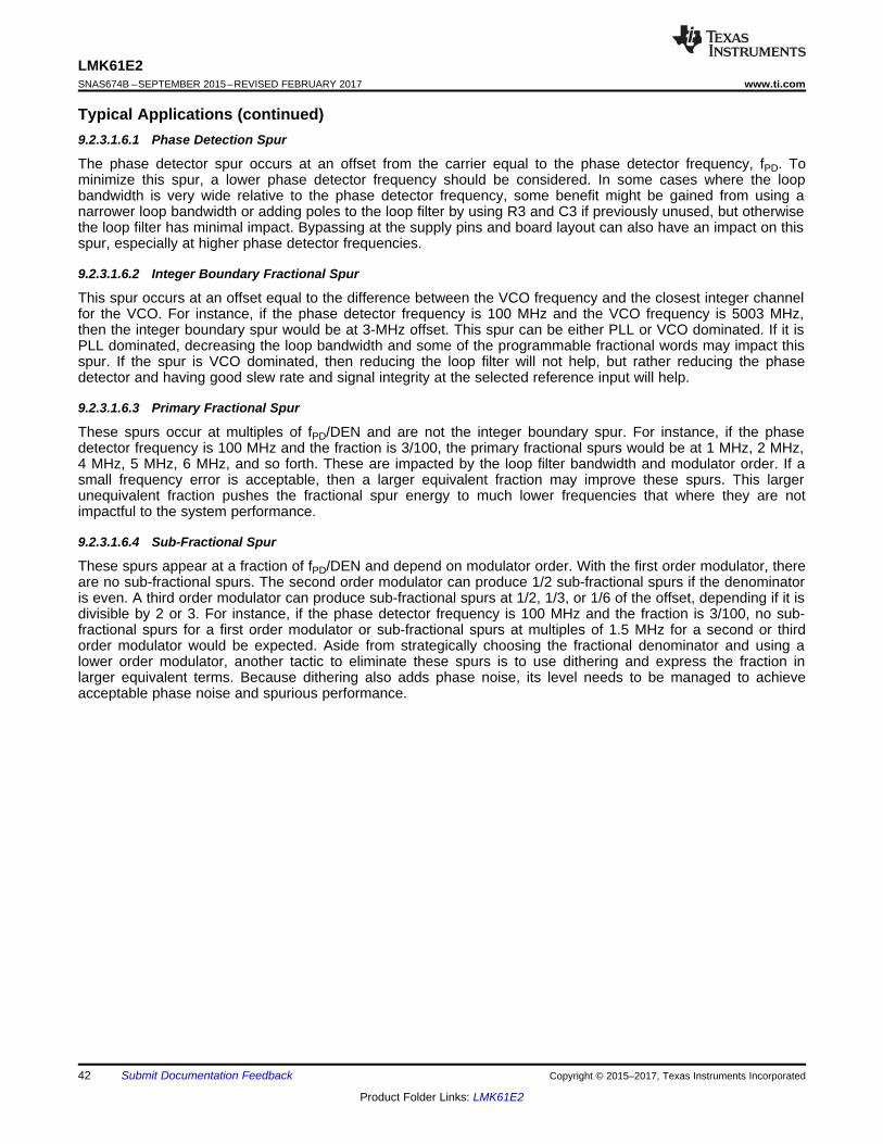
42
LMK61E2SNAS674B –SEPTEMBER 2015–REVISED FEBRUARY 2017 www.ti.com
Product Folder Links: LMK61E2
Submit Documentation Feedback Copyright © 2015–2017, Texas Instruments Incorporated
Typical Applications (continued)9.2.3.1.6.1 Phase Detection Spur
The phase detector spur occurs at an offset from the carrier equal to the phase detector frequency, fPD. Tominimize this spur, a lower phase detector frequency should be considered. In some cases where the loopbandwidth is very wide relative to the phase detector frequency, some benefit might be gained from using anarrower loop bandwidth or adding poles to the loop filter by using R3 and C3 if previously unused, but otherwisethe loop filter has minimal impact. Bypassing at the supply pins and board layout can also have an impact on thisspur, especially at higher phase detector frequencies.
9.2.3.1.6.2 Integer Boundary Fractional Spur
This spur occurs at an offset equal to the difference between the VCO frequency and the closest integer channelfor the VCO. For instance, if the phase detector frequency is 100 MHz and the VCO frequency is 5003 MHz,then the integer boundary spur would be at 3-MHz offset. This spur can be either PLL or VCO dominated. If it isPLL dominated, decreasing the loop bandwidth and some of the programmable fractional words may impact thisspur. If the spur is VCO dominated, then reducing the loop filter will not help, but rather reducing the phasedetector and having good slew rate and signal integrity at the selected reference input will help.
9.2.3.1.6.3 Primary Fractional Spur
These spurs occur at multiples of fPD/DEN and are not the integer boundary spur. For instance, if the phasedetector frequency is 100 MHz and the fraction is 3/100, the primary fractional spurs would be at 1 MHz, 2 MHz,4 MHz, 5 MHz, 6 MHz, and so forth. These are impacted by the loop filter bandwidth and modulator order. If asmall frequency error is acceptable, then a larger equivalent fraction may improve these spurs. This largerunequivalent fraction pushes the fractional spur energy to much lower frequencies that where they are notimpactful to the system performance.
9.2.3.1.6.4 Sub-Fractional Spur
These spurs appear at a fraction of fPD/DEN and depend on modulator order. With the first order modulator, thereare no sub-fractional spurs. The second order modulator can produce 1/2 sub-fractional spurs if the denominatoris even. A third order modulator can produce sub-fractional spurs at 1/2, 1/3, or 1/6 of the offset, depending if it isdivisible by 2 or 3. For instance, if the phase detector frequency is 100 MHz and the fraction is 3/100, no sub-fractional spurs for a first order modulator or sub-fractional spurs at multiples of 1.5 MHz for a second or thirdorder modulator would be expected. Aside from strategically choosing the fractional denominator and using alower order modulator, another tactic to eliminate these spurs is to use dithering and express the fraction inlarger equivalent terms. Because dithering also adds phase noise, its level needs to be managed to achieveacceptable phase noise and spurious performance.
43
LMK61E2www.ti.com SNAS674B –SEPTEMBER 2015–REVISED FEBRUARY 2017
Product Folder Links: LMK61E2
Submit Documentation FeedbackCopyright © 2015–2017, Texas Instruments Incorporated
Typical Applications (continued)Table 2 summarizes spur and mitigation techniques.
Table 2. Spur and Mitigation TechniquesSPUR TYPE OFFSET WAYS TO REDUCE TRADE-OFFS
Phase Detector fPD Reduce Phase DetectorFrequency.
Although reducing the phasedetector frequency does improvethis spur, it also degrades phase
noise.Integer Boundary fVCO mod fPD Methods for PLL Dominated
Spurs
Reducing the loop bandwidthmay degrade the total integrated
noise if the bandwidth is toonarrow.
- Avoid the worst case VCOfrequencies if possible.
- Ensure good slew rate andsignal integrity at reference input.
- Reduce loop bandwidth oradd more filter poles to suppress
out of band spurs.Methods for VCO Dominated
Spurs
Reducing the phase detectormay degrade the phase noise.
- Avoid the worst case VCOfrequencies if possible.
- Reduce Phase DetectorFrequency.
- Ensure good slew rate andsignal integrity at reference input.
Primary Fractional fPD/DEN - Decrease Loop Bandwidth. Decreasing the loop bandwidthmay degrade in-band phase
noise. Also, larger unequivalentfractions don’t always reduce
spurs.
- Change Modulator Order.- Use Larger Unequivalent
Fractions.
Sub-Fractional fPD/DEN/k k=2,3, or 6 - Use Dithering.
Dithering and larger fractionsmay increase phase noise.
- Use Larger EquivalentFractions.
- Use Larger UnequivalentFractions.
- Reduce Modulator Order.- Eliminate factors of 2 or 3 in
denominator.
10 Power Supply RecommendationsFor best electrical performance of the LMK61E2 device, it is preferred to use a combination of 10 µF, 1 µF, and0.1 µF on its power supply bypass network. ITI also recommends using component side mounting of the powersupply bypass capacitors and it is best to use 0201 or 0402 body size capacitors to facilitate signal routing. Keepthe connections between the bypass capacitors and the power supply on the device as short as possible. Groundthe other side of the capacitor using a low impedance connection to the ground plane. Figure 34 shows thelayout recommendation for power supply decoupling of LMK61E2.
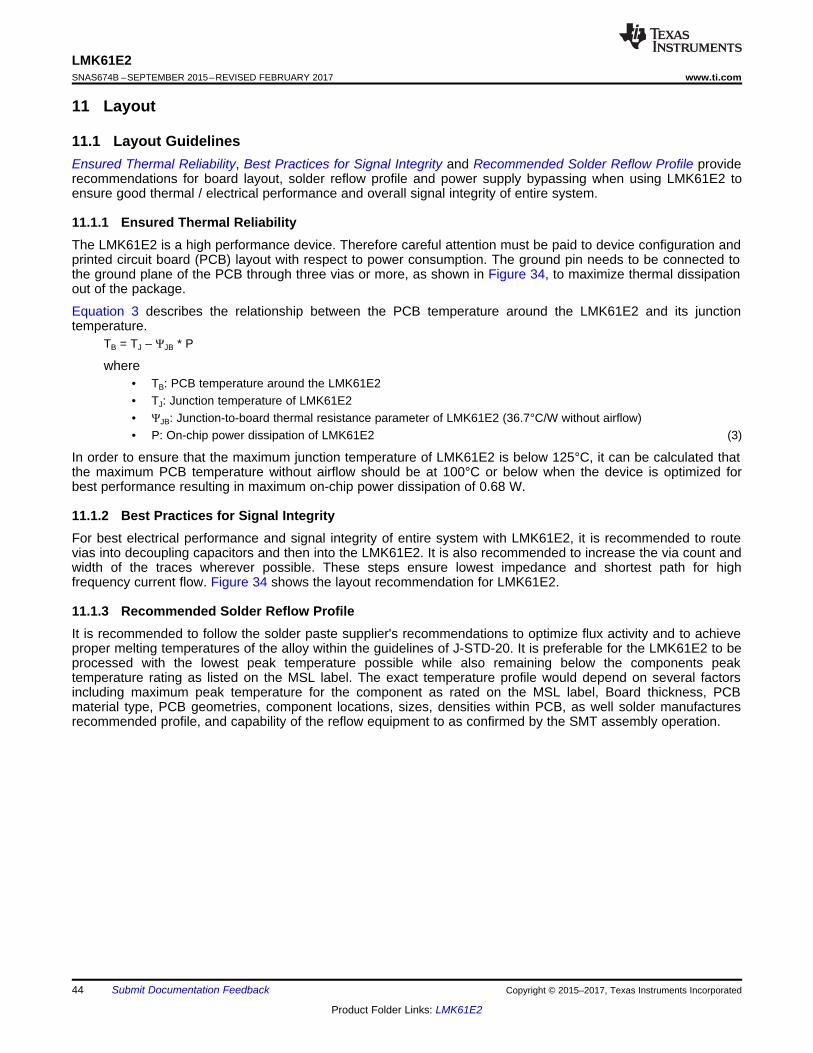
44
LMK61E2SNAS674B –SEPTEMBER 2015–REVISED FEBRUARY 2017 www.ti.com
Product Folder Links: LMK61E2
Submit Documentation Feedback Copyright © 2015–2017, Texas Instruments Incorporated
11 Layout
11.1 Layout GuidelinesEnsured Thermal Reliability, Best Practices for Signal Integrity and Recommended Solder Reflow Profile providerecommendations for board layout, solder reflow profile and power supply bypassing when using LMK61E2 toensure good thermal / electrical performance and overall signal integrity of entire system.
11.1.1 Ensured Thermal ReliabilityThe LMK61E2 is a high performance device. Therefore careful attention must be paid to device configuration andprinted circuit board (PCB) layout with respect to power consumption. The ground pin needs to be connected tothe ground plane of the PCB through three vias or more, as shown in Figure 34, to maximize thermal dissipationout of the package.
Equation 3 describes the relationship between the PCB temperature around the LMK61E2 and its junctiontemperature.
TB = TJ – ΨJB * P
where• TB: PCB temperature around the LMK61E2• TJ: Junction temperature of LMK61E2• ΨJB: Junction-to-board thermal resistance parameter of LMK61E2 (36.7°C/W without airflow)• P: On-chip power dissipation of LMK61E2 (3)
In order to ensure that the maximum junction temperature of LMK61E2 is below 125°C, it can be calculated thatthe maximum PCB temperature without airflow should be at 100°C or below when the device is optimized forbest performance resulting in maximum on-chip power dissipation of 0.68 W.
11.1.2 Best Practices for Signal IntegrityFor best electrical performance and signal integrity of entire system with LMK61E2, it is recommended to routevias into decoupling capacitors and then into the LMK61E2. It is also recommended to increase the via count andwidth of the traces wherever possible. These steps ensure lowest impedance and shortest path for highfrequency current flow. Figure 34 shows the layout recommendation for LMK61E2.
11.1.3 Recommended Solder Reflow ProfileIt is recommended to follow the solder paste supplier's recommendations to optimize flux activity and to achieveproper melting temperatures of the alloy within the guidelines of J-STD-20. It is preferable for the LMK61E2 to beprocessed with the lowest peak temperature possible while also remaining below the components peaktemperature rating as listed on the MSL label. The exact temperature profile would depend on several factorsincluding maximum peak temperature for the component as rated on the MSL label, Board thickness, PCBmaterial type, PCB geometries, component locations, sizes, densities within PCB, as well solder manufacturesrecommended profile, and capability of the reflow equipment to as confirmed by the SMT assembly operation.
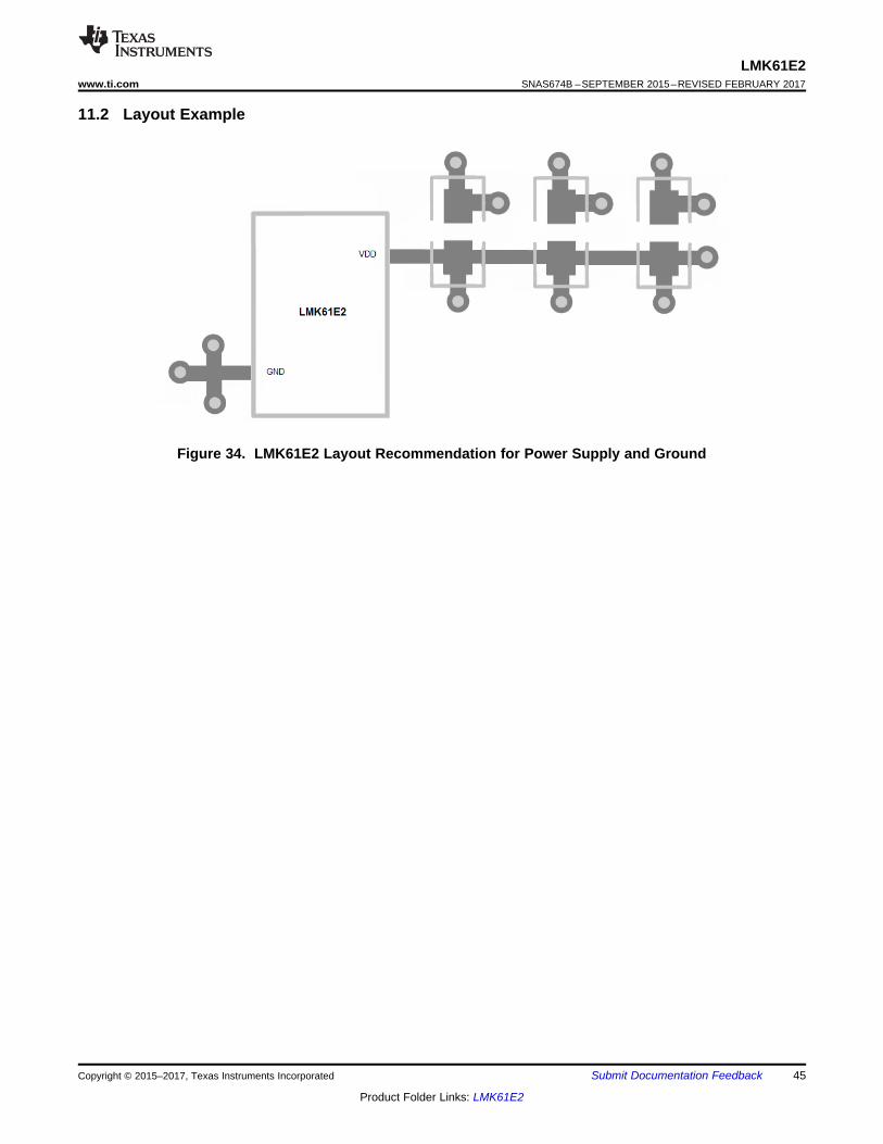
45
LMK61E2www.ti.com SNAS674B –SEPTEMBER 2015–REVISED FEBRUARY 2017
Product Folder Links: LMK61E2
Submit Documentation FeedbackCopyright © 2015–2017, Texas Instruments Incorporated
11.2 Layout Example
Figure 34. LMK61E2 Layout Recommendation for Power Supply and Ground

46
LMK61E2SNAS674B –SEPTEMBER 2015–REVISED FEBRUARY 2017 www.ti.com
Product Folder Links: LMK61E2
Submit Documentation Feedback Copyright © 2015–2017, Texas Instruments Incorporated
12 Device and Documentation Support
12.1 Device Support
12.1.1 Development SupportFor development support, see the following:• WEBENCH Clock Architect Tool• CodeLoader
12.1.1.1 Custom Design With WEBENCH® ToolsClick here to create a custom design using the LMK61E2 device with the WEBENCH® Power Designer.1. Start by entering the input voltage (VIN), output voltage (VOUT), and output current (IOUT) requirements.2. Optimize the design for key parameters such as efficiency, footprint, and cost using the optimizer dial.3. Compare the generated design with other possible solutions from Texas Instruments.
The WEBENCH Power Designer provides a customized schematic along with a list of materials with real-timepricing and component availability.
In most cases, these actions are available:• Run electrical simulations to see important waveforms and circuit performance• Run thermal simulations to understand board thermal performance• Export customized schematic and layout into popular CAD formats• Print PDF reports for the design, and share the design with colleagues
Get more information about WEBENCH tools at www.ti.com/WEBENCH.
12.2 Documentation Support
12.2.1 Related DocumentationFor related documentation, see the following:• Clock Design Tool (SNAU082)• PLL Performance, Simulation, and Design (SNAA106)• Semiconductor and IC Package Thermal Metrics (SPRA953)
12.3 Receiving Notification of Documentation UpdatesTo receive notification of documentation updates, navigate to the device product folder on ti.com. In the upperright corner, click on Alert me to register and receive a weekly digest of any product information that haschanged. For change details, review the revision history included in any revised document.
12.4 Community ResourcesThe following links connect to TI community resources. Linked contents are provided "AS IS" by the respectivecontributors. They do not constitute TI specifications and do not necessarily reflect TI's views; see TI's Terms ofUse.
TI E2E™ Online Community TI's Engineer-to-Engineer (E2E) Community. Created to foster collaborationamong engineers. At e2e.ti.com, you can ask questions, share knowledge, explore ideas and helpsolve problems with fellow engineers.
Design Support TI's Design Support Quickly find helpful E2E forums along with design support tools andcontact information for technical support.
12.5 TrademarksPLLatinum, E2E are trademarks of Texas Instruments.WEBENCH is a registered trademark of Texas Instruments.All other trademarks are the property of their respective owners.
47
LMK61E2www.ti.com SNAS674B –SEPTEMBER 2015–REVISED FEBRUARY 2017
Product Folder Links: LMK61E2
Submit Documentation FeedbackCopyright © 2015–2017, Texas Instruments Incorporated
12.6 Electrostatic Discharge CautionThese devices have limited built-in ESD protection. The leads should be shorted together or the device placed in conductive foamduring storage or handling to prevent electrostatic damage to the MOS gates.
12.7 GlossarySLYZ022 — TI Glossary.
This glossary lists and explains terms, acronyms, and definitions.
13 Mechanical, Packaging, and Orderable InformationThe following pages include mechanical, packaging, and orderable information. This information is the mostcurrent data available for the designated devices. This data is subject to change without notice and revision ofthis document. For browser-based versions of this data sheet, refer to the left-hand navigation.
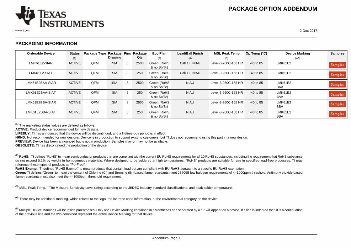
PACKAGE OPTION ADDENDUM
www.ti.com 2-Dec-2017
Addendum-Page 1
PACKAGING INFORMATION
Orderable Device Status(1)
Package Type PackageDrawing
Pins PackageQty
Eco Plan(2)
Lead/Ball Finish(6)
MSL Peak Temp(3)
Op Temp (°C) Device Marking(4/5)
Samples
LMK61E2-SIAR ACTIVE QFM SIA 8 2500 Green (RoHS& no Sb/Br)
Call TI | NIAU Level-3-260C-168 HR -40 to 85 LMK61E2
LMK61E2-SIAT ACTIVE QFM SIA 8 250 Green (RoHS& no Sb/Br)
Call TI | NIAU Level-3-260C-168 HR -40 to 85 LMK61E2
LMK61E2BAA-SIAR ACTIVE QFM SIA 8 2500 Green (RoHS& no Sb/Br)
NIAU Level-3-260C-168 HR -40 to 85 LMK61E2BAA
LMK61E2BAA-SIAT ACTIVE QFM SIA 8 250 Green (RoHS& no Sb/Br)
NIAU Level-3-260C-168 HR -40 to 85 LMK61E2BAA
LMK61E2BBA-SIAR ACTIVE QFM SIA 8 2500 Green (RoHS& no Sb/Br)
NIAU Level-3-260C-168 HR -40 to 85 LMK61E2BBA
LMK61E2BBA-SIAT ACTIVE QFM SIA 8 250 Green (RoHS& no Sb/Br)
NIAU Level-3-260C-168 HR -40 to 85 LMK61E2BBA
(1) The marketing status values are defined as follows:ACTIVE: Product device recommended for new designs.LIFEBUY: TI has announced that the device will be discontinued, and a lifetime-buy period is in effect.NRND: Not recommended for new designs. Device is in production to support existing customers, but TI does not recommend using this part in a new design.PREVIEW: Device has been announced but is not in production. Samples may or may not be available.OBSOLETE: TI has discontinued the production of the device.
(2) RoHS: TI defines "RoHS" to mean semiconductor products that are compliant with the current EU RoHS requirements for all 10 RoHS substances, including the requirement that RoHS substancedo not exceed 0.1% by weight in homogeneous materials. Where designed to be soldered at high temperatures, "RoHS" products are suitable for use in specified lead-free processes. TI mayreference these types of products as "Pb-Free".RoHS Exempt: TI defines "RoHS Exempt" to mean products that contain lead but are compliant with EU RoHS pursuant to a specific EU RoHS exemption.Green: TI defines "Green" to mean the content of Chlorine (Cl) and Bromine (Br) based flame retardants meet JS709B low halogen requirements of <=1000ppm threshold. Antimony trioxide basedflame retardants must also meet the <=1000ppm threshold requirement.
(3) MSL, Peak Temp. - The Moisture Sensitivity Level rating according to the JEDEC industry standard classifications, and peak solder temperature.
(4) There may be additional marking, which relates to the logo, the lot trace code information, or the environmental category on the device.
(5) Multiple Device Markings will be inside parentheses. Only one Device Marking contained in parentheses and separated by a "~" will appear on a device. If a line is indented then it is a continuationof the previous line and the two combined represent the entire Device Marking for that device.
PACKAGE OPTION ADDENDUM
www.ti.com 2-Dec-2017
Addendum-Page 2
(6) Lead/Ball Finish - Orderable Devices may have multiple material finish options. Finish options are separated by a vertical ruled line. Lead/Ball Finish values may wrap to two lines if the finishvalue exceeds the maximum column width.
Important Information and Disclaimer:The information provided on this page represents TI's knowledge and belief as of the date that it is provided. TI bases its knowledge and belief on informationprovided by third parties, and makes no representation or warranty as to the accuracy of such information. Efforts are underway to better integrate information from third parties. TI has taken andcontinues to take reasonable steps to provide representative and accurate information but may not have conducted destructive testing or chemical analysis on incoming materials and chemicals.TI and TI suppliers consider certain information to be proprietary, and thus CAS numbers and other limited information may not be available for release.
In no event shall TI's liability arising out of such information exceed the total purchase price of the TI part(s) at issue in this document sold by TI to Customer on an annual basis.
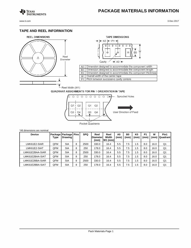
TAPE AND REEL INFORMATION
*All dimensions are nominal
Device PackageType
PackageDrawing
Pins SPQ ReelDiameter
(mm)
ReelWidth
W1 (mm)
A0(mm)
B0(mm)
K0(mm)
P1(mm)
W(mm)
Pin1Quadrant
LMK61E2-SIAR QFM SIA 8 2500 330.0 16.4 5.5 7.5 1.5 8.0 16.0 Q1
LMK61E2-SIAT QFM SIA 8 250 178.0 16.4 5.5 7.5 1.5 8.0 16.0 Q1
LMK61E2BAA-SIAR QFM SIA 8 2500 330.0 16.4 5.5 7.5 1.5 8.0 16.0 Q1
LMK61E2BAA-SIAT QFM SIA 8 250 178.0 16.4 5.5 7.5 1.5 8.0 16.0 Q1
LMK61E2BBA-SIAR QFM SIA 8 2500 330.0 16.4 5.5 7.5 1.5 8.0 16.0 Q1
LMK61E2BBA-SIAT QFM SIA 8 250 178.0 16.4 5.5 7.5 1.5 8.0 16.0 Q1
PACKAGE MATERIALS INFORMATION
www.ti.com 3-Dec-2017
Pack Materials-Page 1
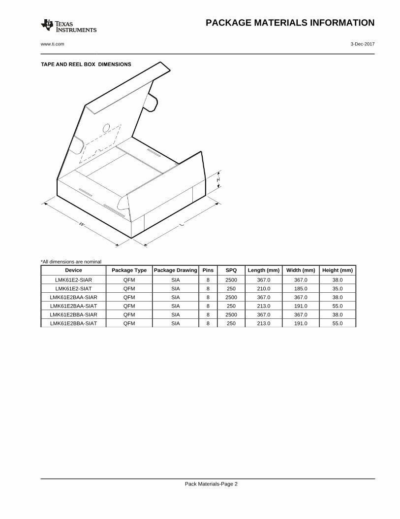
*All dimensions are nominal
Device Package Type Package Drawing Pins SPQ Length (mm) Width (mm) Height (mm)
LMK61E2-SIAR QFM SIA 8 2500 367.0 367.0 38.0
LMK61E2-SIAT QFM SIA 8 250 210.0 185.0 35.0
LMK61E2BAA-SIAR QFM SIA 8 2500 367.0 367.0 38.0
LMK61E2BAA-SIAT QFM SIA 8 250 213.0 191.0 55.0
LMK61E2BBA-SIAR QFM SIA 8 2500 367.0 367.0 38.0
LMK61E2BBA-SIAT QFM SIA 8 250 213.0 191.0 55.0
PACKAGE MATERIALS INFORMATION
www.ti.com 3-Dec-2017
Pack Materials-Page 2
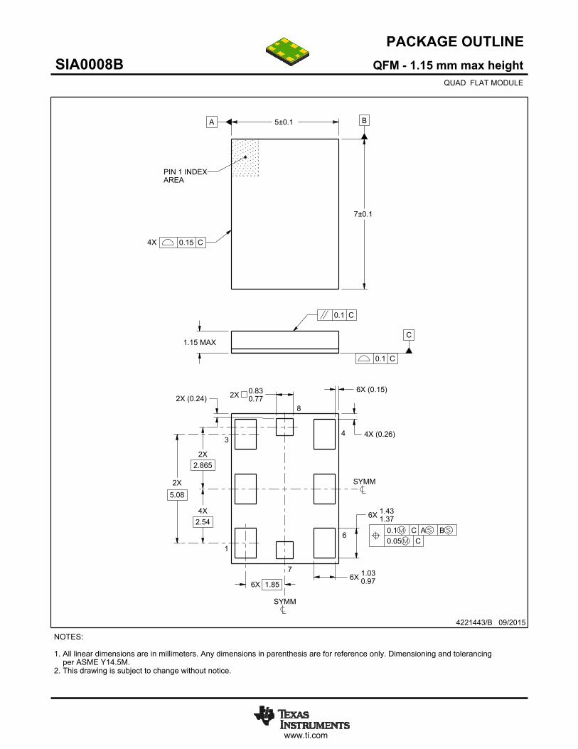
www.ti.com
PACKAGE OUTLINE
C
2X5.08
4X2.54
6X (0.15)
6X 1.030.97
2X 0.830.77
1.15 MAX
6X 1.431.37
2X2.865
6X 1.85
A 5±0.1 B
7±0.1
4X (0.26)
2X (0.24)
QFM - 1.15 mm max heightSIA0008BQUAD FLAT MODULE
4221443/B 09/2015
PIN 1 INDEXAREA
0.15 C4X
0.1 C
0.1 C
0.1 C A B0.05 C
1
34
7
8
SYMM
SYMM
NOTES: 1. All linear dimensions are in millimeters. Any dimensions in parenthesis are for reference only. Dimensioning and tolerancing per ASME Y14.5M.2. This drawing is subject to change without notice.
6
SCALE 1.900
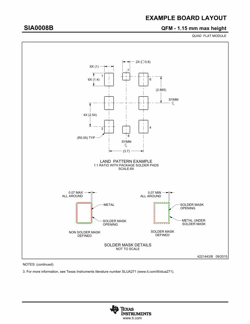
www.ti.com
EXAMPLE BOARD LAYOUT
6X (1)
0.07 MAXALL AROUND
0.07 MINALL AROUND
6X (1.4)
(3.7)
4X (2.54)
(2.865)
2X ( 0.8)
(R ) TYP0.05
QFM - 1.15 mm max heightSIA0008BQUAD FLAT MODULE
4221443/B 09/2015
SYMM
SYMM
1
3 4
7
LAND PATTERN EXAMPLE1:1 RATIO WITH PACKAGE SOLDER PADS
SCALE:8X
8
6
NOTES: (continued) 3. For more information, see Texas Instruments literature number SLUA271 (www.ti.com/lit/slua271).
METAL
SOLDER MASKOPENING
NON SOLDER MASKDEFINED
SOLDER MASK DETAILSNOT TO SCALE
METAL UNDERSOLDER MASK
SOLDER MASKOPENING
SOLDER MASKDEFINED
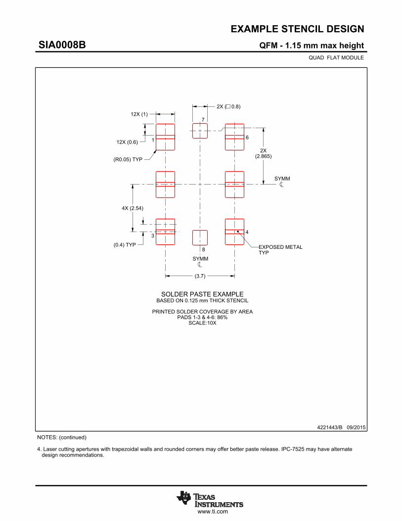
www.ti.com
EXAMPLE STENCIL DESIGN
12X (0.6)
2X ( 0.8)12X (1)
4X (2.54)
(3.7)
2X(2.865)(R ) TYP0.05
(0.4) TYP
QFM - 1.15 mm max heightSIA0008BQUAD FLAT MODULE
4221443/B 09/2015
NOTES: (continued) 4. Laser cutting apertures with trapezoidal walls and rounded corners may offer better paste release. IPC-7525 may have alternate design recommendations.
SYMM
SYMM
SOLDER PASTE EXAMPLEBASED ON 0.125 mm THICK STENCIL
PRINTED SOLDER COVERAGE BY AREA
PADS 1-3 & 4-6: 86%SCALE:10X
1
34
7
8
6
EXPOSED METALTYP

IMPORTANT NOTICE
Texas Instruments Incorporated (TI) reserves the right to make corrections, enhancements, improvements and other changes to itssemiconductor products and services per JESD46, latest issue, and to discontinue any product or service per JESD48, latest issue. Buyersshould obtain the latest relevant information before placing orders and should verify that such information is current and complete.TI’s published terms of sale for semiconductor products (http://www.ti.com/sc/docs/stdterms.htm) apply to the sale of packaged integratedcircuit products that TI has qualified and released to market. Additional terms may apply to the use or sale of other types of TI products andservices.Reproduction of significant portions of TI information in TI data sheets is permissible only if reproduction is without alteration and isaccompanied by all associated warranties, conditions, limitations, and notices. TI is not responsible or liable for such reproduceddocumentation. Information of third parties may be subject to additional restrictions. Resale of TI products or services with statementsdifferent from or beyond the parameters stated by TI for that product or service voids all express and any implied warranties for theassociated TI product or service and is an unfair and deceptive business practice. TI is not responsible or liable for any such statements.Buyers and others who are developing systems that incorporate TI products (collectively, “Designers”) understand and agree that Designersremain responsible for using their independent analysis, evaluation and judgment in designing their applications and that Designers havefull and exclusive responsibility to assure the safety of Designers' applications and compliance of their applications (and of all TI productsused in or for Designers’ applications) with all applicable regulations, laws and other applicable requirements. Designer represents that, withrespect to their applications, Designer has all the necessary expertise to create and implement safeguards that (1) anticipate dangerousconsequences of failures, (2) monitor failures and their consequences, and (3) lessen the likelihood of failures that might cause harm andtake appropriate actions. Designer agrees that prior to using or distributing any applications that include TI products, Designer willthoroughly test such applications and the functionality of such TI products as used in such applications.TI’s provision of technical, application or other design advice, quality characterization, reliability data or other services or information,including, but not limited to, reference designs and materials relating to evaluation modules, (collectively, “TI Resources”) are intended toassist designers who are developing applications that incorporate TI products; by downloading, accessing or using TI Resources in anyway, Designer (individually or, if Designer is acting on behalf of a company, Designer’s company) agrees to use any particular TI Resourcesolely for this purpose and subject to the terms of this Notice.TI’s provision of TI Resources does not expand or otherwise alter TI’s applicable published warranties or warranty disclaimers for TIproducts, and no additional obligations or liabilities arise from TI providing such TI Resources. TI reserves the right to make corrections,enhancements, improvements and other changes to its TI Resources. TI has not conducted any testing other than that specificallydescribed in the published documentation for a particular TI Resource.Designer is authorized to use, copy and modify any individual TI Resource only in connection with the development of applications thatinclude the TI product(s) identified in such TI Resource. NO OTHER LICENSE, EXPRESS OR IMPLIED, BY ESTOPPEL OR OTHERWISETO ANY OTHER TI INTELLECTUAL PROPERTY RIGHT, AND NO LICENSE TO ANY TECHNOLOGY OR INTELLECTUAL PROPERTYRIGHT OF TI OR ANY THIRD PARTY IS GRANTED HEREIN, including but not limited to any patent right, copyright, mask work right, orother intellectual property right relating to any combination, machine, or process in which TI products or services are used. Informationregarding or referencing third-party products or services does not constitute a license to use such products or services, or a warranty orendorsement thereof. Use of TI Resources may require a license from a third party under the patents or other intellectual property of thethird party, or a license from TI under the patents or other intellectual property of TI.TI RESOURCES ARE PROVIDED “AS IS” AND WITH ALL FAULTS. TI DISCLAIMS ALL OTHER WARRANTIES ORREPRESENTATIONS, EXPRESS OR IMPLIED, REGARDING RESOURCES OR USE THEREOF, INCLUDING BUT NOT LIMITED TOACCURACY OR COMPLETENESS, TITLE, ANY EPIDEMIC FAILURE WARRANTY AND ANY IMPLIED WARRANTIES OFMERCHANTABILITY, FITNESS FOR A PARTICULAR PURPOSE, AND NON-INFRINGEMENT OF ANY THIRD PARTY INTELLECTUALPROPERTY RIGHTS. TI SHALL NOT BE LIABLE FOR AND SHALL NOT DEFEND OR INDEMNIFY DESIGNER AGAINST ANY CLAIM,INCLUDING BUT NOT LIMITED TO ANY INFRINGEMENT CLAIM THAT RELATES TO OR IS BASED ON ANY COMBINATION OFPRODUCTS EVEN IF DESCRIBED IN TI RESOURCES OR OTHERWISE. IN NO EVENT SHALL TI BE LIABLE FOR ANY ACTUAL,DIRECT, SPECIAL, COLLATERAL, INDIRECT, PUNITIVE, INCIDENTAL, CONSEQUENTIAL OR EXEMPLARY DAMAGES INCONNECTION WITH OR ARISING OUT OF TI RESOURCES OR USE THEREOF, AND REGARDLESS OF WHETHER TI HAS BEENADVISED OF THE POSSIBILITY OF SUCH DAMAGES.Unless TI has explicitly designated an individual product as meeting the requirements of a particular industry standard (e.g., ISO/TS 16949and ISO 26262), TI is not responsible for any failure to meet such industry standard requirements.Where TI specifically promotes products as facilitating functional safety or as compliant with industry functional safety standards, suchproducts are intended to help enable customers to design and create their own applications that meet applicable functional safety standardsand requirements. Using products in an application does not by itself establish any safety features in the application. Designers mustensure compliance with safety-related requirements and standards applicable to their applications. Designer may not use any TI products inlife-critical medical equipment unless authorized officers of the parties have executed a special contract specifically governing such use.Life-critical medical equipment is medical equipment where failure of such equipment would cause serious bodily injury or death (e.g., lifesupport, pacemakers, defibrillators, heart pumps, neurostimulators, and implantables). Such equipment includes, without limitation, allmedical devices identified by the U.S. Food and Drug Administration as Class III devices and equivalent classifications outside the U.S.TI may expressly designate certain products as completing a particular qualification (e.g., Q100, Military Grade, or Enhanced Product).Designers agree that it has the necessary expertise to select the product with the appropriate qualification designation for their applicationsand that proper product selection is at Designers’ own risk. Designers are solely responsible for compliance with all legal and regulatoryrequirements in connection with such selection.Designer will fully indemnify TI and its representatives against any damages, costs, losses, and/or liabilities arising out of Designer’s non-compliance with the terms and provisions of this Notice.
Mailing Address: Texas Instruments, Post Office Box 655303, Dallas, Texas 75265Copyright © 2017, Texas Instruments Incorporated