Embed Size (px)
Citation preview
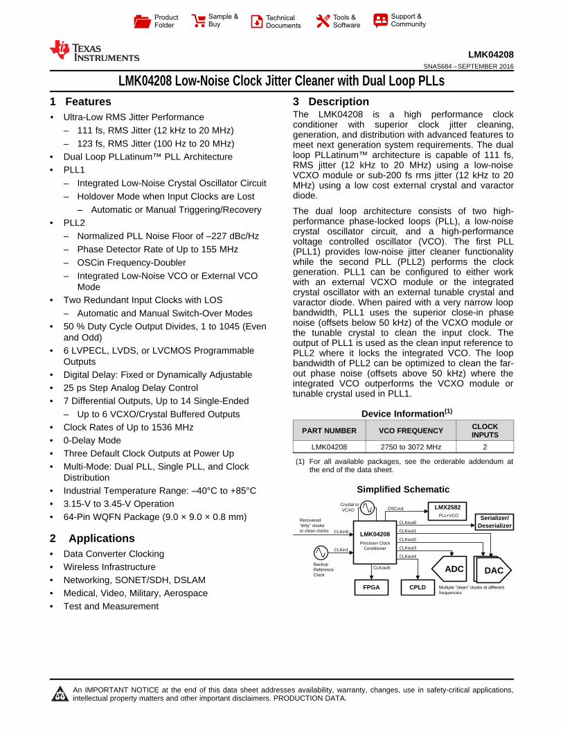
Recovered ³GLUW\´FORFNV
or clean clocks
0XOWLSOH³FOHDQ´FORFNVDWGLIIHUHQW
frequencies
CLKout2
CLKout3
CLKout0
FPGA
CLKin0
Crystal or VCXO
CLKin1
OSCout
CLKout5 DACADC
LMX2582PLL+VCO Serializer/
DeserializerLMK04208Precision Clock
Conditioner
CLKout1
CPLD
CLKout4
Backup Reference Clock
Product
Folder
Sample &Buy
Technical
Documents
Tools &
Software
Support &Community
An IMPORTANT NOTICE at the end of this data sheet addresses availability, warranty, changes, use in safety-critical applications,intellectual property matters and other important disclaimers. PRODUCTION DATA.
LMK04208SNAS684 –SEPTEMBER 2016
LMK04208 Low-Noise Clock Jitter Cleaner with Dual Loop PLLs
1
1 Features1• Ultra-Low RMS Jitter Performance
– 111 fs, RMS Jitter (12 kHz to 20 MHz)– 123 fs, RMS Jitter (100 Hz to 20 MHz)
• Dual Loop PLLatinum™ PLL Architecture• PLL1
– Integrated Low-Noise Crystal Oscillator Circuit– Holdover Mode when Input Clocks are Lost
– Automatic or Manual Triggering/Recovery• PLL2
– Normalized PLL Noise Floor of –227 dBc/Hz– Phase Detector Rate of Up to 155 MHz– OSCin Frequency-Doubler– Integrated Low-Noise VCO or External VCO
Mode• Two Redundant Input Clocks with LOS
– Automatic and Manual Switch-Over Modes• 50 % Duty Cycle Output Divides, 1 to 1045 (Even
and Odd)• 6 LVPECL, LVDS, or LVCMOS Programmable
Outputs• Digital Delay: Fixed or Dynamically Adjustable• 25 ps Step Analog Delay Control• 7 Differential Outputs, Up to 14 Single-Ended
– Up to 6 VCXO/Crystal Buffered Outputs• Clock Rates of Up to 1536 MHz• 0-Delay Mode• Three Default Clock Outputs at Power Up• Multi-Mode: Dual PLL, Single PLL, and Clock
Distribution• Industrial Temperature Range: –40°C to +85°C• 3.15-V to 3.45-V Operation• 64-Pin WQFN Package (9.0 × 9.0 × 0.8 mm)
2 Applications• Data Converter Clocking• Wireless Infrastructure• Networking, SONET/SDH, DSLAM• Medical, Video, Military, Aerospace• Test and Measurement
3 DescriptionThe LMK04208 is a high performance clockconditioner with superior clock jitter cleaning,generation, and distribution with advanced features tomeet next generation system requirements. The dualloop PLLatinum™ architecture is capable of 111 fs,RMS jitter (12 kHz to 20 MHz) using a low-noiseVCXO module or sub-200 fs rms jitter (12 kHz to 20MHz) using a low cost external crystal and varactordiode.
The dual loop architecture consists of two high-performance phase-locked loops (PLL), a low-noisecrystal oscillator circuit, and a high-performancevoltage controlled oscillator (VCO). The first PLL(PLL1) provides low-noise jitter cleaner functionalitywhile the second PLL (PLL2) performs the clockgeneration. PLL1 can be configured to either workwith an external VCXO module or the integratedcrystal oscillator with an external tunable crystal andvaractor diode. When paired with a very narrow loopbandwidth, PLL1 uses the superior close-in phasenoise (offsets below 50 kHz) of the VCXO module orthe tunable crystal to clean the input clock. Theoutput of PLL1 is used as the clean input reference toPLL2 where it locks the integrated VCO. The loopbandwidth of PLL2 can be optimized to clean the far-out phase noise (offsets above 50 kHz) where theintegrated VCO outperforms the VCXO module ortunable crystal used in PLL1.
Device Information(1)
PART NUMBER VCO FREQUENCY CLOCKINPUTS
LMK04208 2750 to 3072 MHz 2
(1) For all available packages, see the orderable addendum atthe end of the data sheet.
Simplified Schematic
2
LMK04208SNAS684 –SEPTEMBER 2016 www.ti.com
Product Folder Links: LMK04208
Submit Documentation Feedback Copyright © 2016, Texas Instruments Incorporated
Table of Contents1 Features .................................................................. 12 Applications ........................................................... 13 Description ............................................................. 14 Revision History..................................................... 25 Pin Configuration and Functions ......................... 36 Specifications......................................................... 5
6.1 Absolute Maximum Ratings ...................................... 56.2 ESD Ratings.............................................................. 56.3 Recommended Operating Conditions....................... 56.4 Thermal Information .................................................. 66.5 Electrical Characteristics........................................... 76.6 Timing Requirements .............................................. 136.7 Typical Characteristics ........................................... 15
7 Parameter Measurement Information ................ 167.1 Charge Pump Current Specification Definitions...... 167.2 Differential Voltage Measurement Terminology...... 17
8 Detailed Description ............................................ 188.1 Overview ................................................................. 188.2 Functional Block Diagram ....................................... 228.3 Feature Description................................................. 238.4 Device Functional Modes........................................ 438.5 Programming........................................................... 488.6 Register Maps ......................................................... 52
9 Application and Implementation ........................ 969.1 Application Information............................................ 969.2 Typical Applications .............................................. 1139.3 System Examples ................................................. 1219.4 Do's and Don'ts..................................................... 123
10 Power Supply Recommendations ................... 12410.1 Pin Connection Recommendations..................... 12410.2 Current Consumption and Power Dissipation
Calculations............................................................ 12611 Layout................................................................. 128
11.1 Layout Guidelines ............................................... 12811.2 Layout Example .................................................. 129
12 Device and Documentation Support ............... 13012.1 Device Support.................................................... 13012.2 Documentation Support ...................................... 13012.3 Receiving Notification of Documentation
Updates.................................................................. 13012.4 Community Resources........................................ 13012.5 Trademarks ......................................................... 13012.6 Electrostatic Discharge Caution.......................... 13012.7 Glossary .............................................................. 130
13 Mechanical, Packaging, and OrderableInformation ......................................................... 130
4 Revision History
DATE REVISION NOTESSeptember 2016 * Initial release.
CL
Ko
ut4
NC
CL
Ko
ut5
*
Sta
tus_
CL
Kin
0
CL
Ko
ut4
*
NC
Vcc1
2
CL
Ko
ut5
NC
NC
Sta
tus_
CL
Kin
1
Vcc1
3
DAP
Top Down View
CL
Ko
ut3
*
Vcc11
NC
NC
NC
Vcc2
Vcc3
NC
Vcc4
NC
CL
Ko
ut2
*
CL
Ko
ut2
GN
D
FB
CL
Kin
/Fin
/CL
Kin
1
FB
CL
Kin
*/F
in*/
CL
Kin
1*
Sta
tus_
Ho
ldo
ve
r
CL
Kin
0
CL
Kin
0*
Vcc5
NC
Vcc7
CPout2
Vcc9
CLKuWire
OSCin*
OSCout
OSCout*
Vcc8
LEuWire
DATAuWire
Vcc10
CLKout3
CPout1
Status_LD
Vcc6
OSCin
NC
NC
NC
CLKout0*
NC
CLKout0
NC
SYNC
NC
NC
Vcc1
LDObyp1
LDObyp2
CLKout1
CLKout1*
NC
48
47
46
45
44
43
42
41
40
39
38
37
36
35
34
33
17 1918 20 21 22 23 24 25 26 27 28 29 30 31 32
1
2
3
4
5
6
7
8
9
10
11
12
13
14
15
16
64 6263 61 60 59 58 57 56 55 54 53 52 51 50 49
3
LMK04208www.ti.com SNAS684 –SEPTEMBER 2016
Product Folder Links: LMK04208
Submit Documentation FeedbackCopyright © 2016, Texas Instruments Incorporated
(1) See Pin Connection Recommendations.
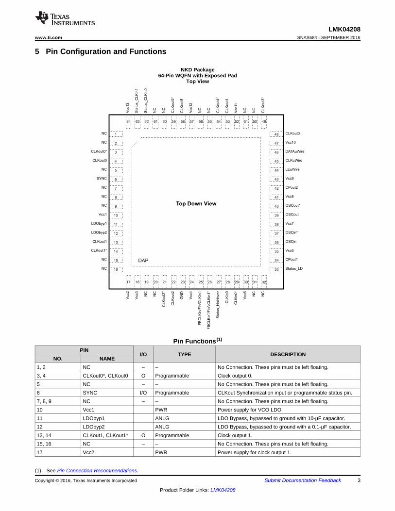
5 Pin Configuration and Functions
NKD Package64-Pin WQFN with Exposed Pad
Top View
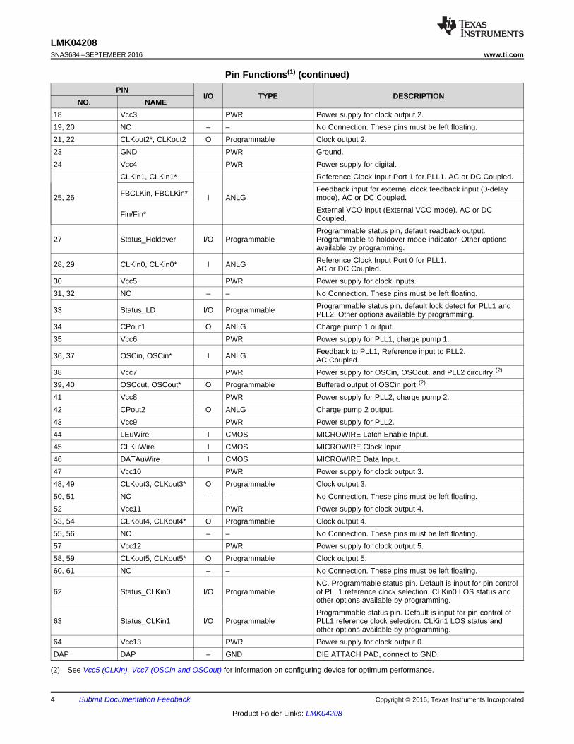
Pin Functions (1)
PINI/O TYPE DESCRIPTION
NO. NAME1, 2 NC – – No Connection. These pins must be left floating.3, 4 CLKout0*, CLKout0 O Programmable Clock output 0.5 NC – – No Connection. These pins must be left floating.6 SYNC I/O Programmable CLKout Synchronization input or programmable status pin.7, 8, 9 NC – – No Connection. These pins must be left floating.10 Vcc1 PWR Power supply for VCO LDO.11 LDObyp1 ANLG LDO Bypass, bypassed to ground with 10-µF capacitor.12 LDObyp2 ANLG LDO Bypass, bypassed to ground with a 0.1-µF capacitor.13, 14 CLKout1, CLKout1* O Programmable Clock output 1.15, 16 NC – – No Connection. These pins must be left floating.17 Vcc2 PWR Power supply for clock output 1.
4
LMK04208SNAS684 –SEPTEMBER 2016 www.ti.com
Product Folder Links: LMK04208
Submit Documentation Feedback Copyright © 2016, Texas Instruments Incorporated
Pin Functions(1) (continued)PIN
I/O TYPE DESCRIPTIONNO. NAME
(2) See Vcc5 (CLKin), Vcc7 (OSCin and OSCout) for information on configuring device for optimum performance.
18 Vcc3 PWR Power supply for clock output 2.19, 20 NC – – No Connection. These pins must be left floating.21, 22 CLKout2*, CLKout2 O Programmable Clock output 2.23 GND PWR Ground.24 Vcc4 PWR Power supply for digital.
25, 26
CLKin1, CLKin1*
I ANLG
Reference Clock Input Port 1 for PLL1. AC or DC Coupled.
FBCLKin, FBCLKin* Feedback input for external clock feedback input (0-delaymode). AC or DC Coupled.
Fin/Fin* External VCO input (External VCO mode). AC or DCCoupled.
27 Status_Holdover I/O ProgrammableProgrammable status pin, default readback output.Programmable to holdover mode indicator. Other optionsavailable by programming.
28, 29 CLKin0, CLKin0* I ANLG Reference Clock Input Port 0 for PLL1.AC or DC Coupled.
30 Vcc5 PWR Power supply for clock inputs.31, 32 NC – – No Connection. These pins must be left floating.
33 Status_LD I/O Programmable Programmable status pin, default lock detect for PLL1 andPLL2. Other options available by programming.
34 CPout1 O ANLG Charge pump 1 output.35 Vcc6 PWR Power supply for PLL1, charge pump 1.
36, 37 OSCin, OSCin* I ANLG Feedback to PLL1, Reference input to PLL2.AC Coupled.
38 Vcc7 PWR Power supply for OSCin, OSCout, and PLL2 circuitry. (2)
39, 40 OSCout, OSCout* O Programmable Buffered output of OSCin port. (2)
41 Vcc8 PWR Power supply for PLL2, charge pump 2.42 CPout2 O ANLG Charge pump 2 output.43 Vcc9 PWR Power supply for PLL2.44 LEuWire I CMOS MICROWIRE Latch Enable Input.45 CLKuWire I CMOS MICROWIRE Clock Input.46 DATAuWire I CMOS MICROWIRE Data Input.47 Vcc10 PWR Power supply for clock output 3.48, 49 CLKout3, CLKout3* O Programmable Clock output 3.50, 51 NC – – No Connection. These pins must be left floating.52 Vcc11 PWR Power supply for clock output 4.53, 54 CLKout4, CLKout4* O Programmable Clock output 4.55, 56 NC – – No Connection. These pins must be left floating.57 Vcc12 PWR Power supply for clock output 5.58, 59 CLKout5, CLKout5* O Programmable Clock output 5.60, 61 NC – – No Connection. These pins must be left floating.
62 Status_CLKin0 I/O ProgrammableNC. Programmable status pin. Default is input for pin controlof PLL1 reference clock selection. CLKin0 LOS status andother options available by programming.
63 Status_CLKin1 I/O ProgrammableProgrammable status pin. Default is input for pin control ofPLL1 reference clock selection. CLKin1 LOS status andother options available by programming.
64 Vcc13 PWR Power supply for clock output 0.DAP DAP – GND DIE ATTACH PAD, connect to GND.
5
LMK04208www.ti.com SNAS684 –SEPTEMBER 2016
Product Folder Links: LMK04208
Submit Documentation FeedbackCopyright © 2016, Texas Instruments Incorporated
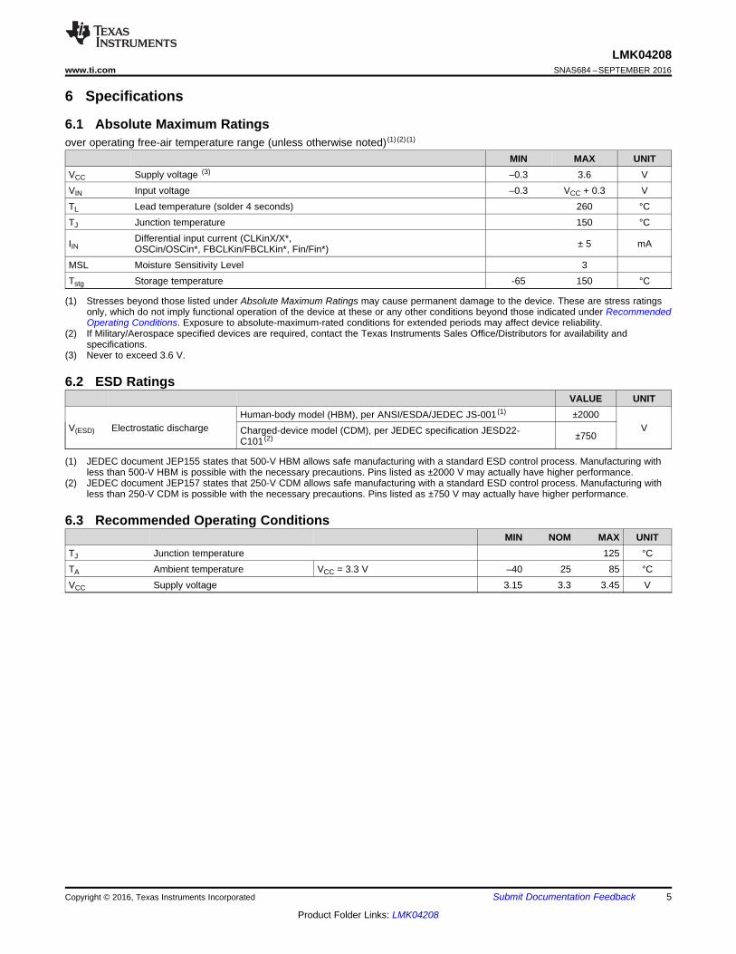
(1) Stresses beyond those listed under Absolute Maximum Ratings may cause permanent damage to the device. These are stress ratingsonly, which do not imply functional operation of the device at these or any other conditions beyond those indicated under RecommendedOperating Conditions. Exposure to absolute-maximum-rated conditions for extended periods may affect device reliability.
(2) If Military/Aerospace specified devices are required, contact the Texas Instruments Sales Office/Distributors for availability andspecifications.
(3) Never to exceed 3.6 V.
6 Specifications
6.1 Absolute Maximum Ratingsover operating free-air temperature range (unless otherwise noted) (1) (2) (1)
MIN MAX UNITVCC Supply voltage (3) –0.3 3.6 VVIN Input voltage –0.3 VCC + 0.3 VTL Lead temperature (solder 4 seconds) 260 °CTJ Junction temperature 150 °C
IINDifferential input current (CLKinX/X*,OSCin/OSCin*, FBCLKin/FBCLKin*, Fin/Fin*) ± 5 mA
MSL Moisture Sensitivity Level 3Tstg Storage temperature -65 150 °C
(1) JEDEC document JEP155 states that 500-V HBM allows safe manufacturing with a standard ESD control process. Manufacturing withless than 500-V HBM is possible with the necessary precautions. Pins listed as ±2000 V may actually have higher performance.
(2) JEDEC document JEP157 states that 250-V CDM allows safe manufacturing with a standard ESD control process. Manufacturing withless than 250-V CDM is possible with the necessary precautions. Pins listed as ±750 V may actually have higher performance.
6.2 ESD RatingsVALUE UNIT
V(ESD) Electrostatic dischargeHuman-body model (HBM), per ANSI/ESDA/JEDEC JS-001 (1) ±2000
VCharged-device model (CDM), per JEDEC specification JESD22-C101 (2) ±750
6.3 Recommended Operating ConditionsMIN NOM MAX UNIT
TJ Junction temperature 125 °CTA Ambient temperature VCC = 3.3 V –40 25 85 °CVCC Supply voltage 3.15 3.3 3.45 V
6
LMK04208SNAS684 –SEPTEMBER 2016 www.ti.com
Product Folder Links: LMK04208
Submit Documentation Feedback Copyright © 2016, Texas Instruments Incorporated
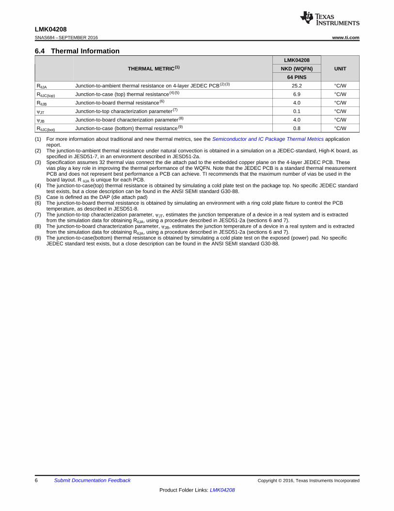
(1) For more information about traditional and new thermal metrics, see the Semiconductor and IC Package Thermal Metrics applicationreport.
(2) The junction-to-ambient thermal resistance under natural convection is obtained in a simulation on a JEDEC-standard, High-K board, asspecified in JESD51-7, in an environment described in JESD51-2a.
(3) Specification assumes 32 thermal vias connect the die attach pad to the embedded copper plane on the 4-layer JEDEC PCB. Thesevias play a key role in improving the thermal performance of the WQFN. Note that the JEDEC PCB is a standard thermal measurementPCB and does not represent best performance a PCB can achieve. TI recommends that the maximum number of vias be used in theboard layout. R θJA is unique for each PCB.
(4) The junction-to-case(top) thermal resistance is obtained by simulating a cold plate test on the package top. No specific JEDEC standardtest exists, but a close description can be found in the ANSI SEMI standard G30-88.
(5) Case is defined as the DAP (die attach pad)(6) The junction-to-board thermal resistance is obtained by simulating an environment with a ring cold plate fixture to control the PCB
temperature, as described in JESD51-8.(7) The junction-to-top characterization parameter, ψJT, estimates the junction temperature of a device in a real system and is extracted
from the simulation data for obtaining RθJA, using a procedure described in JESD51-2a (sections 6 and 7).(8) The junction-to-board characterization parameter, ψJB, estimates the junction temperature of a device in a real system and is extracted
from the simulation data for obtaining RθJA, using a procedure described in JESD51-2a (sections 6 and 7).(9) The junction-to-case(bottom) thermal resistance is obtained by simulating a cold plate test on the exposed (power) pad. No specific
JEDEC standard test exists, but a close description can be found in the ANSI SEMI standard G30-88.
6.4 Thermal Information
THERMAL METRIC (1)LMK04208
UNITNKD (WQFN)64 PINS
RθJA Junction-to-ambient thermal resistance on 4-layer JEDEC PCB (2) (3) 25.2 °C/WRθJC(top) Junction-to-case (top) thermal resistance (4) (5) 6.9 °C/WRθJB Junction-to-board thermal resistance (6) 4.0 °C/WψJT Junction-to-top characterization parameter (7) 0.1 °C/WψJB Junction-to-board characterization parameter (8) 4.0 °C/WRθJC(bot) Junction-to-case (bottom) thermal resistance (9) 0.8 °C/W
7
LMK04208www.ti.com SNAS684 –SEPTEMBER 2016
Product Folder Links: LMK04208
Submit Documentation FeedbackCopyright © 2016, Texas Instruments Incorporated
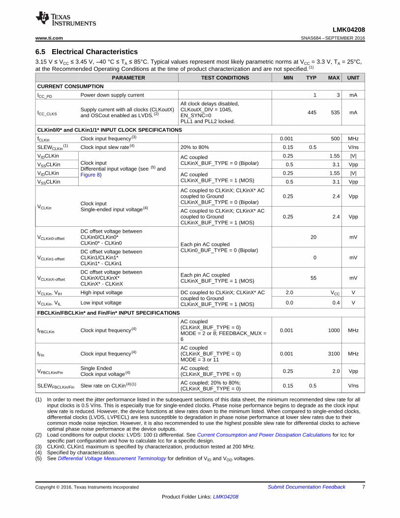
(1) In order to meet the jitter performance listed in the subsequent sections of this data sheet, the minimum recommended slew rate for allinput clocks is 0.5 V/ns. This is especially true for single-ended clocks. Phase noise performance begins to degrade as the clock inputslew rate is reduced. However, the device functions at slew rates down to the minimum listed. When compared to single-ended clocks,differential clocks (LVDS, LVPECL) are less susceptible to degradation in phase noise performance at lower slew rates due to theircommon mode noise rejection. However, it is also recommended to use the highest possible slew rate for differential clocks to achieveoptimal phase noise performance at the device outputs.
(2) Load conditions for output clocks: LVDS: 100 Ω differential. See Current Consumption and Power Dissipation Calculations for Icc forspecific part configuration and how to calculate Icc for a specific design.
(3) CLKin0, CLKin1 maximum is specified by characterization, production tested at 200 MHz.(4) Specified by characterization.(5) See Differential Voltage Measurement Terminology for definition of VID and VOD voltages.
6.5 Electrical Characteristics3.15 V ≤ VCC ≤ 3.45 V, –40 °C ≤ TA ≤ 85°C. Typical values represent most likely parametric norms at VCC = 3.3 V, TA = 25°C,at the Recommended Operating Conditions at the time of product characterization and are not specified. (1)
PARAMETER TEST CONDITIONS MIN TYP MAX UNITCURRENT CONSUMPTIONICC_PD Power down supply current 1 3 mA
ICC_CLKSSupply current with all clocks (CLKoutX)and OSCout enabled as LVDS. (2)
All clock delays disabled,CLKoutX_DIV = 1045,EN_SYNC=0PLL1 and PLL2 locked.
445 535 mA
CLKin0/0* and CLKin1/1* INPUT CLOCK SPECIFICATIONSfCLKin Clock input frequency (3) 0.001 500 MHzSLEWCLKin
(1) Clock input slew rate (4) 20% to 80% 0.15 0.5 V/nsVIDCLKin
Clock inputDifferential input voltage (see (5) andFigure 8)
AC coupledCLKinX_BUF_TYPE = 0 (Bipolar)
0.25 1.55 |V|VSSCLKin 0.5 3.1 VppVIDCLKin AC coupled
CLKinX_BUF_TYPE = 1 (MOS)0.25 1.55 |V|
VSSCLKin 0.5 3.1 Vpp
VCLKinClock inputSingle-ended input voltage (4)
AC coupled to CLKinX; CLKinX* ACcoupled to GroundCLKinX_BUF_TYPE = 0 (Bipolar)
0.25 2.4 Vpp
AC coupled to CLKinX; CLKinX* ACcoupled to GroundCLKinX_BUF_TYPE = 1 (MOS)
0.25 2.4 Vpp
VCLKin0-offset
DC offset voltage betweenCLKin0/CLKin0*CLKin0* - CLKin0 Each pin AC coupled
CLKin0_BUF_TYPE = 0 (Bipolar)
20 mV
VCLKin1-offset
DC offset voltage betweenCLKin1/CLKin1*CLKin1* - CLKin1
0 mV
VCLKinX-offset
DC offset voltage betweenCLKinX/CLKinX*CLKinX* - CLKinX
Each pin AC coupledCLKinX_BUF_TYPE = 1 (MOS) 55 mV
VCLKin- VIH High input voltage DC coupled to CLKinX; CLKinX* ACcoupled to GroundCLKinX_BUF_TYPE = 1 (MOS)
2.0 VCC V
VCLKin- VIL Low input voltage 0.0 0.4 V
FBCLKin/FBCLKin* and Fin/Fin* INPUT SPECIFICATIONS
fFBCLKin Clock input frequency (4)
AC coupled(CLKinX_BUF_TYPE = 0)MODE = 2 or 8; FEEDBACK_MUX =6
0.001 1000 MHz
fFin Clock input frequency (4)AC coupled(CLKinX_BUF_TYPE = 0)MODE = 3 or 11
0.001 3100 MHz
VFBCLKin/FinSingle EndedClock input voltage (4)
AC coupled;(CLKinX_BUF_TYPE = 0) 0.25 2.0 Vpp
SLEWFBCLKin/Fin Slew rate on CLKin (4) (1) AC coupled; 20% to 80%;(CLKinX_BUF_TYPE = 0) 0.15 0.5 V/ns

8
LMK04208SNAS684 –SEPTEMBER 2016 www.ti.com
Product Folder Links: LMK04208
Submit Documentation Feedback Copyright © 2016, Texas Instruments Incorporated
Electrical Characteristics (continued)3.15 V ≤ VCC ≤ 3.45 V, –40 °C ≤ TA ≤ 85°C. Typical values represent most likely parametric norms at VCC = 3.3 V, TA = 25°C,at the Recommended Operating Conditions at the time of product characterization and are not specified.(1)
PARAMETER TEST CONDITIONS MIN TYP MAX UNIT
(6) This parameter is programmable(7) A specification in modeling PLL in-band phase noise is the 1/f flicker noise, LPLL_flicker(f), which is dominant close to the carrier. Flicker
noise has a 10 dB/decade slope. PN10kHz is normalized to a 10 kHz offset and a 1 GHz carrier frequency. PN10kHz = LPLL_flicker(10kHz) - 20log(Fout / 1 GHz), where LPLL_flicker(f) is the single side band phase noise of only the flicker noise's contribution to total noise,L(f). To measure LPLL_flicker(f) it is important to be on the 10 dB/decade slope close to the carrier. A high compare frequency and a cleancrystal are important to isolating this noise source from the total phase noise, L(f). LPLL_flicker(f) can be masked by the referenceoscillator performance if a low power or noisy source is used. The total PLL in-band phase noise performance is the sum of LPLL_flicker(f)and LPLL_flat(f).
(8) A specification modeling PLL in-band phase noise. The normalized phase noise contribution of the PLL, LPLL_flat(f), is defined as:PN1HZ=LPLL_flat(f) - 20log(N) - 10log(fPDX). LPLL_flat(f) is the single side band phase noise measured at an offset frequency, f, in a 1 Hzbandwidth and fPDX is the phase detector frequency of the synthesizer. LPLL_flat(f) contributes to the total noise, L(f).
(9) FOSCin maximum frequency specified by characterization. Production tested at 200 MHz.(10) The EN_PLL2_REF_2X bit (Register 13) enables/disables a frequency doubler mode for the PLL2 OSCin path.
PLL1 SPECIFICATIONSfPD1 PLL1 phase detector frequency 40 MHz
ICPout1SOURCE PLL1 chargePump source current (6)
VCPout1 = VCC/2, PLL1_CP_GAIN = 0 100
µAVCPout1 = VCC/2, PLL1_CP_GAIN = 1 200VCPout1 = VCC/2, PLL1_CP_GAIN = 2 400VCPout1 = VCC/2, PLL1_CP_GAIN = 3 1600
ICPout1SINK PLL1 chargePump sink current (6)
VCPout1=VCC/2, PLL1_CP_GAIN = 0 –100
µAVCPout1=VCC/2, PLL1_CP_GAIN = 1 –200VCPout1=VCC/2, PLL1_CP_GAIN = 2 –400VCPout1=VCC/2, PLL1_CP_GAIN = 3 –1600
ICPout1%MIS Charge pumpSink/source mismatch VCPout1 = VCC/2, T = 25 °C 3% 10%
ICPout1VTUNEMagnitude of charge pump currentvariation vs. charge pump voltage
0.5 V < VCPout1 < VCC - 0.5 VTA = 25 °C 4%
ICPout1%TEMP Charge pump current vs.temperature variation 4%
ICPout1 TRI Charge Pump TRI-STATE leakagecurrent 0.5 V < VCPout < VCC - 0.5 V 5 nA
PN10kHz PLL 1/f noise at 10 kHz offset. (7)
Normalized to 1 GHz Output FrequencyPLL1_CP_GAIN = 400 µA –117
dBc/HzPLL1_CP_GAIN = 1600 µA –118
PN1Hz Normalized phase noise contribution (8) PLL1_CP_GAIN = 400 µA –221.5dBc/Hz
PLL1_CP_GAIN = 1600 µA –223PLL2 REFERENCE INPUT (OSCin) SPECIFICATIONSfOSCin PLL2 reference input (9) 500 MHz
SLEWOSCinPLL2 reference clock minimum slew rateon OSCin (4) 20% to 80% 0.15 0.5 V/ns
VOSCin Input voltage for OSCin or OSCin* (4) AC coupled; Single-ended (Unusedpin AC coupled to GND) 0.2 2.4 Vpp
VIDOSCinDifferential voltage swing (see Figure 8) AC coupled
0.2 1.55 |V|VSSOSCin 0.4 3.1 Vpp
VOSCin-offset
DC offset voltage betweenOSCin/OSCin*OSCinX* - OSCinX
Each pin AC coupled 20 mV
fdoubler_max Doubler input frequency (4) EN_PLL2_REF_2X = 1; (10)
OSCin Duty Cycle 40% to 60% 155 MHz
9
LMK04208www.ti.com SNAS684 –SEPTEMBER 2016
Product Folder Links: LMK04208
Submit Documentation FeedbackCopyright © 2016, Texas Instruments Incorporated
Electrical Characteristics (continued)3.15 V ≤ VCC ≤ 3.45 V, –40 °C ≤ TA ≤ 85°C. Typical values represent most likely parametric norms at VCC = 3.3 V, TA = 25°C,at the Recommended Operating Conditions at the time of product characterization and are not specified.(1)
PARAMETER TEST CONDITIONS MIN TYP MAX UNIT
(11) See Application Section discussion of Optional Crystal Oscillator Implementation (OSCin/OSCin*).(12) Maximum Allowable Temperature Drift for Continuous Lock is how far the temperature can drift in either direction from the value it was
at the time that the R30 register was last programmed, and still have the part stay in lock. The action of programming the R30 register,even to the same value, activates a frequency calibration routine. This implies the part works over the entire frequency range, but if thetemperature drifts more than the maximum allowable drift for continuous lock, then it is necessary to reload the R30 register to ensure itstays in lock. Regardless of what temperature the part was initially programmed at, the temperature can never drift outside thefrequency range of -40 °C to 85 °C without violating specifications.
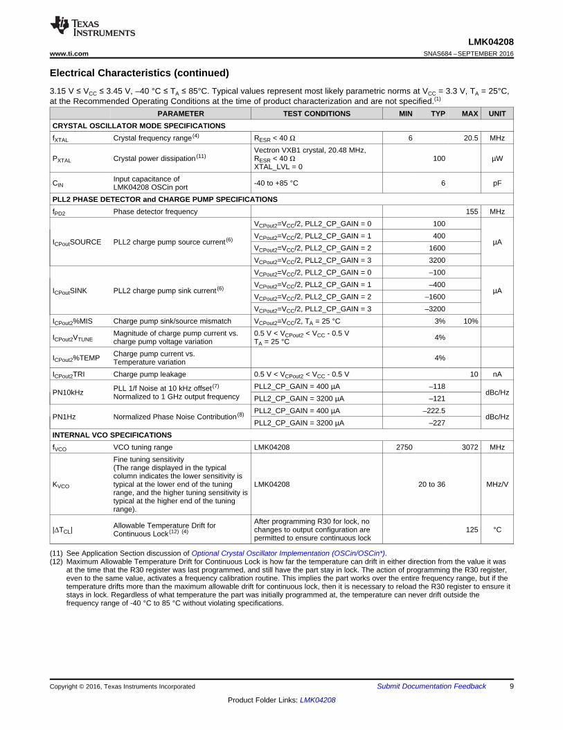
CRYSTAL OSCILLATOR MODE SPECIFICATIONSfXTAL Crystal frequency range (4) RESR < 40 Ω 6 20.5 MHz
PXTAL Crystal power dissipation (11)Vectron VXB1 crystal, 20.48 MHz,RESR < 40 ΩXTAL_LVL = 0
100 µW
CINInput capacitance ofLMK04208 OSCin port -40 to +85 °C 6 pF
PLL2 PHASE DETECTOR and CHARGE PUMP SPECIFICATIONSfPD2 Phase detector frequency 155 MHz
ICPoutSOURCE PLL2 charge pump source current (6)
VCPout2=VCC/2, PLL2_CP_GAIN = 0 100
µAVCPout2=VCC/2, PLL2_CP_GAIN = 1 400VCPout2=VCC/2, PLL2_CP_GAIN = 2 1600VCPout2=VCC/2, PLL2_CP_GAIN = 3 3200
ICPoutSINK PLL2 charge pump sink current (6)
VCPout2=VCC/2, PLL2_CP_GAIN = 0 –100
µAVCPout2=VCC/2, PLL2_CP_GAIN = 1 –400VCPout2=VCC/2, PLL2_CP_GAIN = 2 –1600VCPout2=VCC/2, PLL2_CP_GAIN = 3 –3200
ICPout2%MIS Charge pump sink/source mismatch VCPout2=VCC/2, TA = 25 °C 3% 10%
ICPout2VTUNEMagnitude of charge pump current vs.charge pump voltage variation
0.5 V < VCPout2 < VCC - 0.5 VTA = 25 °C 4%
ICPout2%TEMP Charge pump current vs.Temperature variation 4%
ICPout2TRI Charge pump leakage 0.5 V < VCPout2 < VCC - 0.5 V 10 nA
PN10kHz PLL 1/f Noise at 10 kHz offset (7)
Normalized to 1 GHz output frequencyPLL2_CP_GAIN = 400 µA –118
dBc/HzPLL2_CP_GAIN = 3200 µA –121
PN1Hz Normalized Phase Noise Contribution (8) PLL2_CP_GAIN = 400 µA –222.5dBc/Hz
PLL2_CP_GAIN = 3200 µA –227INTERNAL VCO SPECIFICATIONSfVCO VCO tuning range LMK04208 2750 3072 MHz
KVCO
Fine tuning sensitivity(The range displayed in the typicalcolumn indicates the lower sensitivity istypical at the lower end of the tuningrange, and the higher tuning sensitivity istypical at the higher end of the tuningrange).
LMK04208 20 to 36 MHz/V
|ΔTCL| Allowable Temperature Drift forContinuous Lock (12) (4)
After programming R30 for lock, nochanges to output configuration arepermitted to ensure continuous lock
125 °C
10
LMK04208SNAS684 –SEPTEMBER 2016 www.ti.com
Product Folder Links: LMK04208
Submit Documentation Feedback Copyright © 2016, Texas Instruments Incorporated
Electrical Characteristics (continued)3.15 V ≤ VCC ≤ 3.45 V, –40 °C ≤ TA ≤ 85°C. Typical values represent most likely parametric norms at VCC = 3.3 V, TA = 25°C,at the Recommended Operating Conditions at the time of product characterization and are not specified.(1)
PARAMETER TEST CONDITIONS MIN TYP MAX UNIT
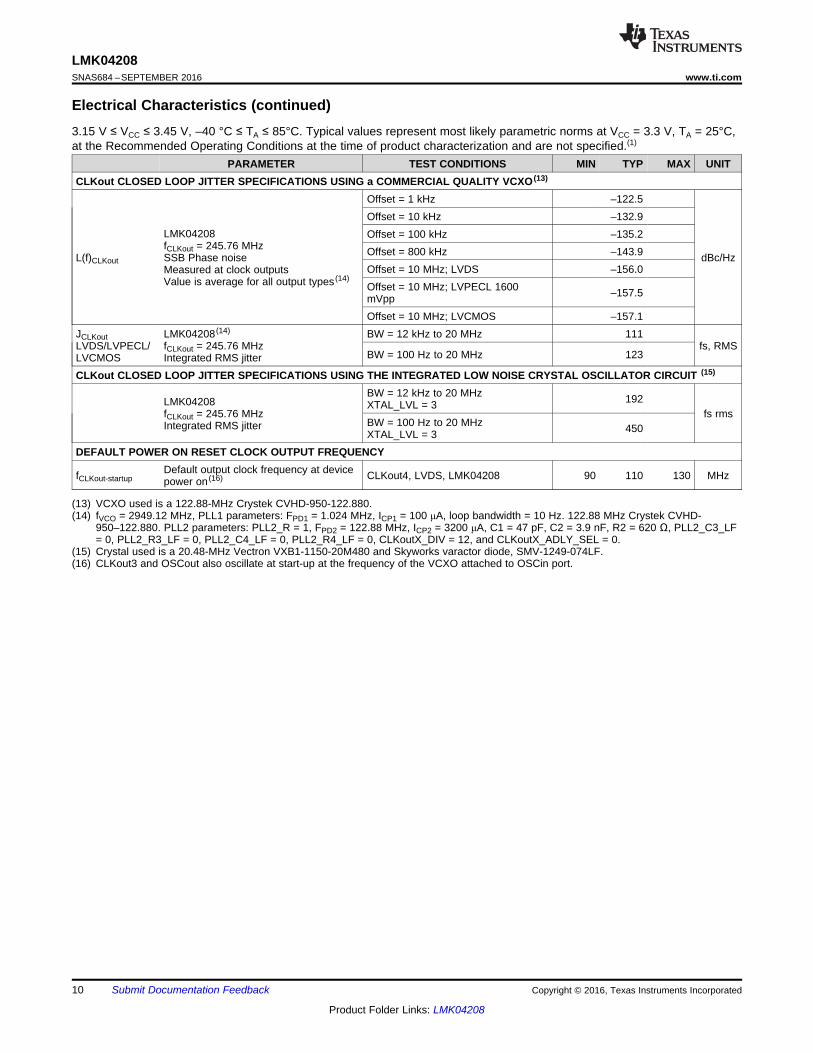
(13) VCXO used is a 122.88-MHz Crystek CVHD-950-122.880.(14) fVCO = 2949.12 MHz, PLL1 parameters: FPD1 = 1.024 MHz, ICP1 = 100 μA, loop bandwidth = 10 Hz. 122.88 MHz Crystek CVHD-
950–122.880. PLL2 parameters: PLL2_R = 1, FPD2 = 122.88 MHz, ICP2 = 3200 μA, C1 = 47 pF, C2 = 3.9 nF, R2 = 620 Ω, PLL2_C3_LF= 0, PLL2_R3_LF = 0, PLL2_C4_LF = 0, PLL2_R4_LF = 0, CLKoutX_DIV = 12, and CLKoutX_ADLY_SEL = 0.
(15) Crystal used is a 20.48-MHz Vectron VXB1-1150-20M480 and Skyworks varactor diode, SMV-1249-074LF.(16) CLKout3 and OSCout also oscillate at start-up at the frequency of the VCXO attached to OSCin port.
CLKout CLOSED LOOP JITTER SPECIFICATIONS USING a COMMERCIAL QUALITY VCXO (13)
L(f)CLKout
LMK04208fCLKout = 245.76 MHzSSB Phase noiseMeasured at clock outputsValue is average for all output types (14)
Offset = 1 kHz –122.5
dBc/Hz
Offset = 10 kHz –132.9Offset = 100 kHz –135.2Offset = 800 kHz –143.9Offset = 10 MHz; LVDS –156.0Offset = 10 MHz; LVPECL 1600mVpp –157.5
Offset = 10 MHz; LVCMOS –157.1JCLKoutLVDS/LVPECL/LVCMOS
LMK04208 (14)
fCLKout = 245.76 MHzIntegrated RMS jitter
BW = 12 kHz to 20 MHz 111fs, RMS
BW = 100 Hz to 20 MHz 123
CLKout CLOSED LOOP JITTER SPECIFICATIONS USING THE INTEGRATED LOW NOISE CRYSTAL OSCILLATOR CIRCUIT (15)
LMK04208fCLKout = 245.76 MHzIntegrated RMS jitter
BW = 12 kHz to 20 MHzXTAL_LVL = 3 192
fs rmsBW = 100 Hz to 20 MHzXTAL_LVL = 3 450
DEFAULT POWER ON RESET CLOCK OUTPUT FREQUENCY
fCLKout-startupDefault output clock frequency at devicepower on (16) CLKout4, LVDS, LMK04208 90 110 130 MHz
11
LMK04208www.ti.com SNAS684 –SEPTEMBER 2016
Product Folder Links: LMK04208
Submit Documentation FeedbackCopyright © 2016, Texas Instruments Incorporated
Electrical Characteristics (continued)3.15 V ≤ VCC ≤ 3.45 V, –40 °C ≤ TA ≤ 85°C. Typical values represent most likely parametric norms at VCC = 3.3 V, TA = 25°C,at the Recommended Operating Conditions at the time of product characterization and are not specified.(1)
PARAMETER TEST CONDITIONS MIN TYP MAX UNIT
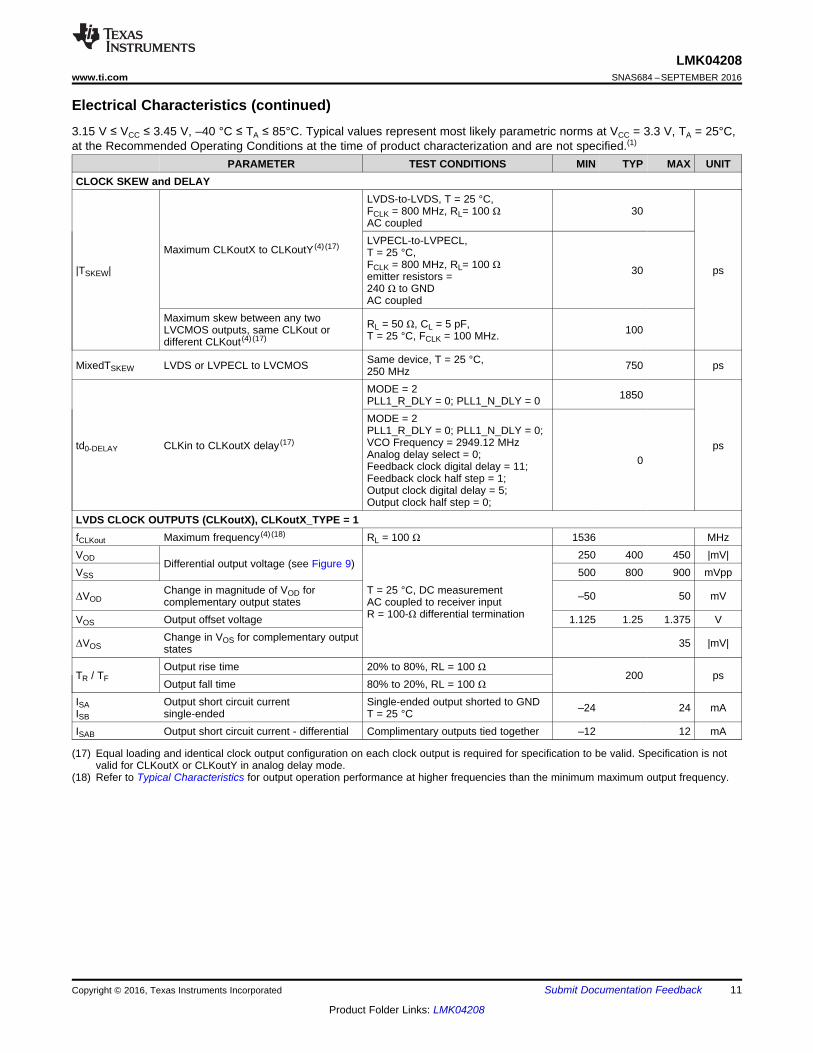
(17) Equal loading and identical clock output configuration on each clock output is required for specification to be valid. Specification is notvalid for CLKoutX or CLKoutY in analog delay mode.
(18) Refer to Typical Characteristics for output operation performance at higher frequencies than the minimum maximum output frequency.
CLOCK SKEW and DELAY
|TSKEW|
Maximum CLKoutX to CLKoutY (4) (17)
LVDS-to-LVDS, T = 25 °C,FCLK = 800 MHz, RL= 100 ΩAC coupled
30
ps
LVPECL-to-LVPECL,T = 25 °C,FCLK = 800 MHz, RL= 100 Ωemitter resistors =240 Ω to GNDAC coupled
30
Maximum skew between any twoLVCMOS outputs, same CLKout ordifferent CLKout (4) (17)
RL = 50 Ω, CL = 5 pF,T = 25 °C, FCLK = 100 MHz. 100
MixedTSKEW LVDS or LVPECL to LVCMOS Same device, T = 25 °C,250 MHz 750 ps
td0-DELAY CLKin to CLKoutX delay (17)
MODE = 2PLL1_R_DLY = 0; PLL1_N_DLY = 0 1850
ps
MODE = 2PLL1_R_DLY = 0; PLL1_N_DLY = 0;VCO Frequency = 2949.12 MHzAnalog delay select = 0;Feedback clock digital delay = 11;Feedback clock half step = 1;Output clock digital delay = 5;Output clock half step = 0;
0
LVDS CLOCK OUTPUTS (CLKoutX), CLKoutX_TYPE = 1fCLKout Maximum frequency (4) (18) RL = 100 Ω 1536 MHzVOD Differential output voltage (see Figure 9)
T = 25 °C, DC measurementAC coupled to receiver inputR = 100-Ω differential termination
250 400 450 |mV|VSS 500 800 900 mVpp
ΔVODChange in magnitude of VOD forcomplementary output states –50 50 mV
VOS Output offset voltage 1.125 1.25 1.375 V
ΔVOSChange in VOS for complementary outputstates 35 |mV|
TR / TFOutput rise time 20% to 80%, RL = 100 Ω
200 psOutput fall time 80% to 20%, RL = 100 Ω
ISAISB
Output short circuit currentsingle-ended
Single-ended output shorted to GNDT = 25 °C –24 24 mA
ISAB Output short circuit current - differential Complimentary outputs tied together –12 12 mA
12
LMK04208SNAS684 –SEPTEMBER 2016 www.ti.com
Product Folder Links: LMK04208
Submit Documentation Feedback Copyright © 2016, Texas Instruments Incorporated
Electrical Characteristics (continued)3.15 V ≤ VCC ≤ 3.45 V, –40 °C ≤ TA ≤ 85°C. Typical values represent most likely parametric norms at VCC = 3.3 V, TA = 25°C,at the Recommended Operating Conditions at the time of product characterization and are not specified.(1)
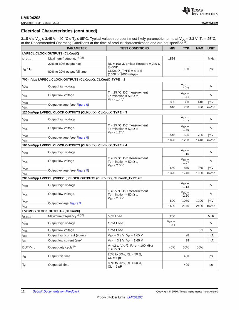
PARAMETER TEST CONDITIONS MIN TYP MAX UNITLVPECL CLOCK OUTPUTS (CLKoutX)fCLKout Maximum frequency (4) (18) 1536 MHz
TR / TF
20% to 80% output rise RL = 100 Ω, emitter resistors = 240 Ωto GNDCLKoutX_TYPE = 4 or 5(1600 or 2000 mVpp)
150 ps80% to 20% output fall time
700-mVpp LVPECL CLOCK OUTPUTS (CLKoutX), CLKoutX_TYPE = 2
VOH Output high voltage
T = 25 °C, DC measurementTermination = 50 Ω toVCC - 1.4 V
VCC –1.03 V
VOL Output low voltage VCC –1.41 V
VOD Output voltage (see Figure 9)305 380 440 |mV|
VSS 610 760 880 mVpp1200-mVpp LVPECL CLOCK OUTPUTS (CLKoutX), CLKoutX_TYPE = 3
VOH Output high voltage
T = 25 °C, DC measurementTermination = 50 Ω toVCC - 1.7 V
VCC –1.07 V
VOL Output low voltage VCC –1.69 V
VOD Output voltage (see Figure 9)545 625 705 |mV|
VSS 1090 1250 1410 mVpp1600-mVpp LVPECL CLOCK OUTPUTS (CLKoutX), CLKoutX_TYPE = 4
VOH Output high voltage
T = 25 °C, DC MeasurementTermination = 50 Ω toVCC - 2.0 V
VCC –1.10 V
VOL Output low voltage VCC –1.97 V
VOD Output voltage (see Figure 9)660 870 965 |mV|
VSS 1320 1740 1930 mVpp2000-mVpp LVPECL (2VPECL) CLOCK OUTPUTS (CLKoutX), CLKoutX_TYPE = 5
VOH Output high voltage
T = 25 °C, DC MeasurementTermination = 50 Ω toVCC - 2.3 V
VCC –1.13 V
VOL Output low voltage VCC –2.20 V
VOD Output voltage Figure 9800 1070 1200 |mV|
VSS 1600 2140 2400 mVppLVCMOS CLOCK OUTPUTS (CLKoutX)fCLKout Maximum frequency (4) (18) 5 pF Load 250 MHz
VOH Output high voltage 1 mA Load VCC –0.1 V
VOL Output low voltage 1 mA Load 0.1 VIOH Output high current (source) VCC = 3.3 V, VO = 1.65 V 28 mAIOL Output low current (sink) VCC = 3.3 V, VO = 1.65 V 28 mA
DUTYCLK Output duty cycle (4) VCC/2 to VCC/2, FCLK = 100 MHzT = 25 °C 45% 50% 55%
TR Output rise time 20% to 80%, RL = 50 Ω,CL = 5 pF 400 ps
TF Output fall time 80% to 20%, RL = 50 Ω,CL = 5 pF 400 ps
13
LMK04208www.ti.com SNAS684 –SEPTEMBER 2016
Product Folder Links: LMK04208
Submit Documentation FeedbackCopyright © 2016, Texas Instruments Incorporated
Electrical Characteristics (continued)3.15 V ≤ VCC ≤ 3.45 V, –40 °C ≤ TA ≤ 85°C. Typical values represent most likely parametric norms at VCC = 3.3 V, TA = 25°C,at the Recommended Operating Conditions at the time of product characterization and are not specified.(1)
PARAMETER TEST CONDITIONS MIN TYP MAX UNITDIGITAL OUTPUTS (Status_CLKinX, Status_LD, Status_Holdover, SYNC)
VOH High-level output voltage IOH = -500 µA VCC –0.4 V
VOL Low-level output voltage IOL = 500 µA 0.4 VDIGITAL INPUTS (Status_CLKinX, SYNC)VIH High-level input voltage 1.6 VCC VVIL Low-level input voltage 0.4 V
IIHHigh-level input currentVIH = VCC
Status_CLKinX_TYPE = 0(High Impedance) –5 5
µAStatus_CLKinX_TYPE = 1(Pull-up) –5 5
Status_CLKinX_TYPE = 2(Pull-down) 10 80
IILLow-level input currentVIL = 0 V
Status_CLKinX_TYPE = 0(High Impedance) –5 5
µAStatus_CLKinX_TYPE = 1(Pull-up) –40 -5
Status_CLKinX_TYPE = 2(Pull-down) –5 5
DIGITAL INPUTS (CLKuWire, DATAuWire, LEuWire)VIH High-level input voltage 1.6 VCC VVIL Low-level input voltage 0.4 VIIH High-level input current VIH = VCC 5 25 µAIIL Low-level input current VIL = 0 –5 5 µA
6.6 Timing RequirementsSee Programming for additional information
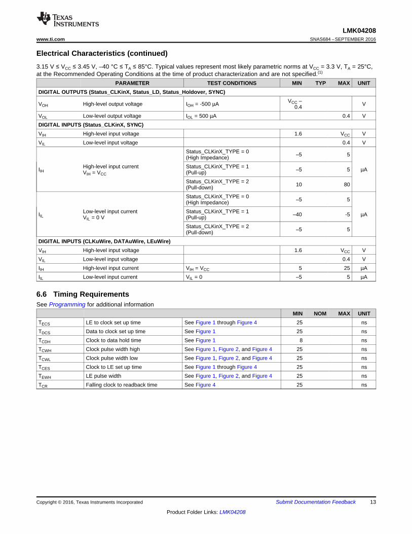
MIN NOM MAX UNITTECS LE to clock set up time See Figure 1 through Figure 4 25 nsTDCS Data to clock set up time See Figure 1 25 nsTCDH Clock to data hold time See Figure 1 8 nsTCWH Clock pulse width high See Figure 1, Figure 2, and Figure 4 25 nsTCWL Clock pulse width low See Figure 1, Figure 2, and Figure 4 25 nsTCES Clock to LE set up time See Figure 1 through Figure 4 25 nsTEWH LE pulse width See Figure 1, Figure 2, and Figure 4 25 nsTCR Falling clock to readback time See Figure 4 25 ns
D26 A0
MSB LSB
DATAuWire
CLKuWire
LEuWireREADBACK_LE = 0
tECS
tEWH
Readback Pin RD0RD24RD26
LEuWireREADBACK_LE = 1
tCWHtCWL
RD25
tCR
RD23
tCR
tECS
Register Write Register Read
tCES
D26 A0
MSB LSB
DATAuWire
CLKuWire
LEuWire
tCEStCES
tECS
D26 A0
MSB LSB
DATAuWire
CLKuWire
LEuWire
tECS
tEWH
tCWHtCWL
tCES
tECStDCS
D26 D25 D24 D23
tCDHtCWH tCWL
D22 D0 A4 A1 A0
MSB LSB
DATAuWire
CLKuWire
LEuWire
tCES
tEWH
tECS
14
LMK04208SNAS684 –SEPTEMBER 2016 www.ti.com
Product Folder Links: LMK04208
Submit Documentation Feedback Copyright © 2016, Texas Instruments Incorporated
Figure 1. MICROWIRE Input Timing Diagram
Figure 2. MICROWIRE Timing Diagram: Extra CLKuWire Pulses for R0 to R5
Figure 3. MICROWIRE Timing Diagram: Extra CLKuWire Pulses for R0 to R5 with LEuWire Asserted
Figure 4. MICROWIRE Readback Timing Diagram
0 500 1000 1500 2000 2500 3000
0
200
400
600
800
1000
1200
VO
D(m
V)
FREQUENCY (MHz)
2000 mVpp
1600 mVpp
0 500 1000 1500 2000 2500 3000
0
50
100
150
200
250
300
350
400
450
500V
OD
(mV
)
FREQUENCY (MHz)0 500 1000 1500 2000 2500 3000
0
200
400
600
800
1000
1200
VO
D(m
V)
FREQUENCY (MHz)
2000 mVpp1600 mVpp1200 mVpp700 mVpp
15
LMK04208www.ti.com SNAS684 –SEPTEMBER 2016
Product Folder Links: LMK04208
Submit Documentation FeedbackCopyright © 2016, Texas Instruments Incorporated
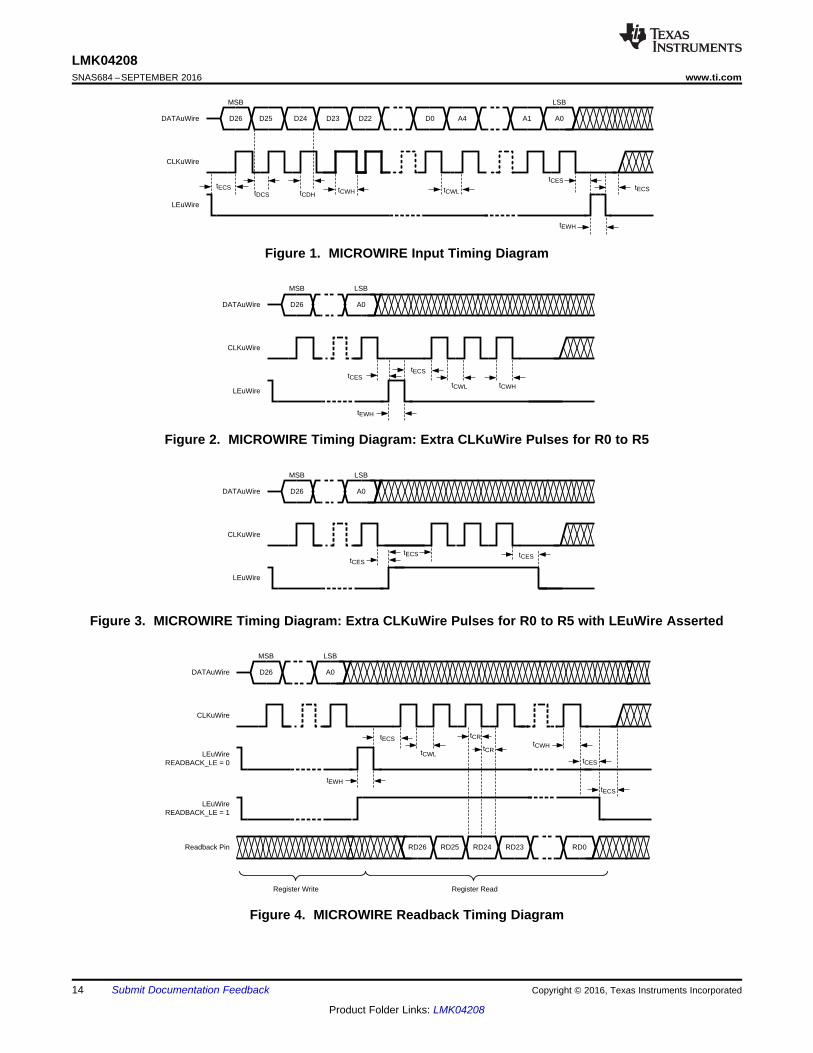
6.7 Typical Characteristics
Figure 5. LVDS VOD vs Frequency Figure 6. LVPECL with 240-Ω Emitter ResistorsVOD vs Frequency
Figure 7. LVPECL with 120-Ω Emitter ResistorsVOD vs Frequency
16
LMK04208SNAS684 –SEPTEMBER 2016 www.ti.com
Product Folder Links: LMK04208
Submit Documentation Feedback Copyright © 2016, Texas Instruments Incorporated
7 Parameter Measurement Information
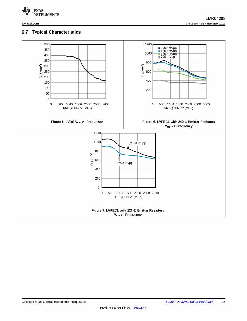
7.1 Charge Pump Current Specification Definitions
I1 = Charge Pump Sink Current at VCPout = VCC - ΔVI2 = Charge Pump Sink Current at VCPout = VCC/2I3 = Charge Pump Sink Current at VCPout = ΔVI4 = Charge Pump Source Current at VCPout = VCC - ΔVI5 = Charge Pump Source Current at VCPout = VCC/2I6 = Charge Pump Source Current at VCPout = ΔVΔV = Voltage offset from the positive and negative supply rails. Defined to be 0.5 V for this device.
7.1.1 Charge Pump Output Current Magnitude Variation Vs. Charge Pump Output Voltage
7.1.2 Charge Pump Sink Current Vs. Charge Pump Output Source Current Mismatch
7.1.3 Charge Pump Output Current Magnitude Variation vs. Ambient Temperature
VA
VB
GND
VOD = | VA - VB | VSS = 2·VOD
VOD Definition VSS Definition for Output
Non-Inverting Clock
Inverting Clock
VOD 2·VOD
VA
VB
GND
VID = | VA - VB | VSS = 2·VID
VID Definition VSS Definition for Input
Non-Inverting Clock
Inverting Clock
VID 2·VID
17
LMK04208www.ti.com SNAS684 –SEPTEMBER 2016
Product Folder Links: LMK04208
Submit Documentation FeedbackCopyright © 2016, Texas Instruments Incorporated
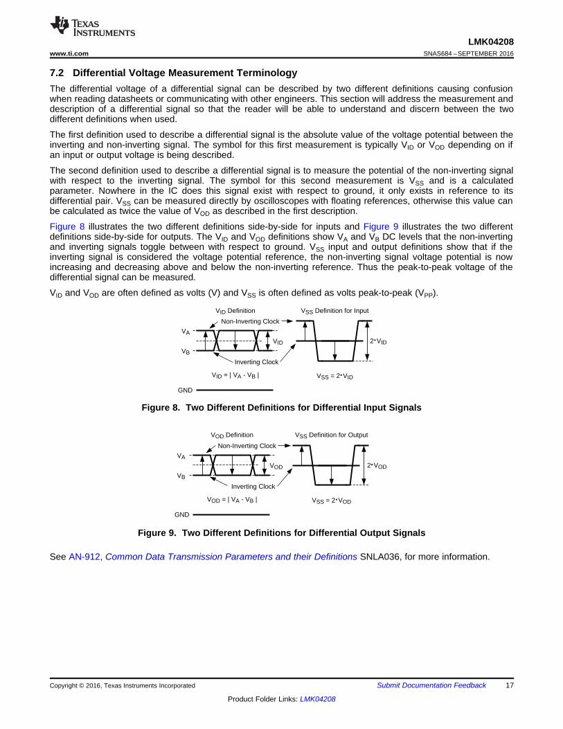
7.2 Differential Voltage Measurement TerminologyThe differential voltage of a differential signal can be described by two different definitions causing confusionwhen reading datasheets or communicating with other engineers. This section will address the measurement anddescription of a differential signal so that the reader will be able to understand and discern between the twodifferent definitions when used.
The first definition used to describe a differential signal is the absolute value of the voltage potential between theinverting and non-inverting signal. The symbol for this first measurement is typically VID or VOD depending on ifan input or output voltage is being described.
The second definition used to describe a differential signal is to measure the potential of the non-inverting signalwith respect to the inverting signal. The symbol for this second measurement is VSS and is a calculatedparameter. Nowhere in the IC does this signal exist with respect to ground, it only exists in reference to itsdifferential pair. VSS can be measured directly by oscilloscopes with floating references, otherwise this value canbe calculated as twice the value of VOD as described in the first description.
Figure 8 illustrates the two different definitions side-by-side for inputs and Figure 9 illustrates the two differentdefinitions side-by-side for outputs. The VID and VOD definitions show VA and VB DC levels that the non-invertingand inverting signals toggle between with respect to ground. VSS input and output definitions show that if theinverting signal is considered the voltage potential reference, the non-inverting signal voltage potential is nowincreasing and decreasing above and below the non-inverting reference. Thus the peak-to-peak voltage of thedifferential signal can be measured.
VID and VOD are often defined as volts (V) and VSS is often defined as volts peak-to-peak (VPP).
Figure 8. Two Different Definitions for Differential Input Signals
Figure 9. Two Different Definitions for Differential Output Signals
See AN-912, Common Data Transmission Parameters and their Definitions SNLA036, for more information.

18
LMK04208SNAS684 –SEPTEMBER 2016 www.ti.com
Product Folder Links: LMK04208
Submit Documentation Feedback Copyright © 2016, Texas Instruments Incorporated
8 Detailed Description
8.1 OverviewIn default mode of operation, dual PLL mode with internal VCO, the Phase Frequency Detector in PLL1compares the active CLKinX reference divided by CLKinX_PreR_DIV and PLL1 R divider with the externalVCXO or crystal attached to the PLL2 OSCin port divided by PLL1 N divider. The external loop filter for PLL1should be narrow to provide an ultra clean reference clock from the external VCXO or crystal to theOSCin/OSCin* pins for PLL2.
The Phase Frequency Detector in PLL2 compares the external VCXO or crystal to the internal VCO after thereference and feedback dividers. The VCXO or crystal on the OSCin input is divided by PLL2 R divider. Thefeedback from the internal VCO is divided by the PLL2 Prescaler, the PLL2 N divider, and optionally the VCOdivider.
The bandwidth of the external loop filter for PLL2 should be designed to be wide enough to take advantage ofthe low in-band phase noise of PLL2 and the low high offset phase noise of the internal VCO. The VCO output isalso placed on the distribution path for the Clock Distribution section. The clock distribution consists of 6 outputs.Each clock output allows the user to select a divide value, a digital delay value, and an analog delay. The 6 clockoutputs drive programmable output buffers. Two clock outputs allow their input signal to be from the OSCin portdirectly.
When a 0-delay mode is used, a clock output will be passed through the feedback mux to the PLL1 N Divider forsynchronization and 0-delay.
When an external VCO mode is used, the Fin port will be used to input an external VCO signal. PLL2 Phasecomparison will now be with this signal divided by the PLL2 N divider and N2 pre-scaler. The VCO divider maynot be used. One less clock input is available when using an external VCO mode.
When a single PLL mode is used, PLL1 is powered down. OSCin is used as a reference to PLL2.
8.1.1 System ArchitectureThe dual loop PLL architecture of the LMK04208 provides the lowest jitter performance over the widest range ofoutput frequencies and phase noise integration bandwidths. The first stage PLL (PLL1) is driven by an externalreference clock and uses an external VCXO or tunable crystal to provide a frequency accurate, low phase noisereference clock for the second stage frequency multiplication PLL (PLL2). PLL1 typically uses a narrow loopbandwidth (10 Hz to 200 Hz) to retain the frequency accuracy of the reference clock input signal while at thesame time suppressing the higher offset frequency phase noise that the reference clock may have accumulatedalong its path or from other circuits. This cleaned reference clock provides the reference input to PLL2.
The low phase noise reference provided to PLL2 allows PLL2 to operate with a wide loop bandwidth (50 kHz to200 kHz). The loop bandwidth for PLL2 is chosen to take advantage of the superior high offset frequency phasenoise profile of the internal VCO and the good low offset frequency phase noise of the reference VCXO ortunable crystal.
Ultra low jitter is achieved by allowing the external VCXO or crystal’s phase noise to dominate the final outputphase noise at low offset frequencies and the internal (or external) VCO’s phase noise to dominate the finaloutput phase noise at high offset frequencies. This results in best overall phase noise and jitter performance.
The LMK04208 allows subsets of the device to be used to increase the flexibility of device. These differentmodes are selected using MODE: Device Mode. For instance:• Dual Loop Mode - Typical use case of LMK04208. CLKinX used as reference input to PLL1, OSCin port is
connected to VCXO or tunable crystal.• Single Loop Mode - Powers down PLL1. OSCin port is used as reference input.• Clock Distribution Mode - Allows input of CLKin1 to be distributed to output with division, digital delay, and
analog delay.
See Device Functional Modes for more information on these modes.
19
LMK04208www.ti.com SNAS684 –SEPTEMBER 2016
Product Folder Links: LMK04208
Submit Documentation FeedbackCopyright © 2016, Texas Instruments Incorporated
Overview (continued)8.1.2 PLL1 Redundant Reference Inputs (CLKin0/CLKin0* and CLKin1/CLKin1*)The LMK04208 has two reference clock inputs for PLL1: CLKin0 and CLKin1. Ref Mux selects CLKin0 orCLKin1. Automatic or manual switching occurs between the inputs.
CLKin0 and CLKin1 each have input dividers. The input divider allows different clock input frequencies to benormalized so that the frequency input to the PLL1 R divider remains constant during automatic switching. Byprogramming these dividers such that the frequency presented to the input of the PLL1 R divider is the sameprevents the user from needing to reprogram the PLL1 R divider when the input reference is changed to anotherCLKin port with a different frequency.
CLKin1 is shared for use as an external 0-delay feedback (FBCLKin), or for use with an external VCO (Fin).
Fast manual switching between reference clocks is possible with external pins Status_CLKin0 andStatus_CLKin1.
8.1.3 PLL1 Tunable Crystal SupportThe LMK04208 integrates a crystal oscillator on PLL1 for use with an external crystal and varactor diode toperform jitter cleaning.
The LMK04208 must be programmed to enable Crystal mode.
8.1.4 VCXO/Crystal Buffered OutputThe LMK04208 provides a dedicated output, OSCout, which is a buffered copy of the PLL2 reference input (seeFunctional Block Diagram for a block diagram of this implementation). The PLL2 reference input is typically a lownoise VCXO or Crystal. When using a VCXO, this output can be used to clock external devices such asmicrocontrollers, FPGAs, CPLDs, and so forth, before the LMK04208 is programmed. See Clock OutputSynchronization and MODE: Device Mode for further reference of these outputs
The OSCout buffer output type is programmable to LVDS, LVPECL, or LVCMOS.
The dedicated output buffer OSCout can output frequency lower than the VCXO or Crystal frequency byprogramming the OSC Divider. The OSC Divider value range is 2 to 8.
Two clock outputs can also be programmed to be driven by OSCin. This allows a total of 2 additional differentialoutputs to be buffered outputs of OSCin. When programmed in this way, a total of 3 differential or 6 single-endedoutputs can be driven by a buffered copy of OSCin.
VCXO/Crystal buffered outputs cannot be synchronized to the VCO clock distribution outputs. The assertion ofSYNC will still cause these outputs to become low temporarily. Since these outputs will turn off and onasynchronously with respect to the VCO sourced clock outputs during a SYNC, it is possible for glitches to occuron the buffered clock outputs when SYNC is asserted and unasserted. If the NO_SYNC_CLKoutX bits are setthese outputs will not be affected by the SYNC event except that the phase relationship will change with theother synchronized clocks unless a buffered clock output is used as a qualification clock during SYNC.
8.1.5 Frequency HoldoverThe LMK04208 supports holdover operation to keep the clock outputs on frequency with minimum drift when thereference is lost until a valid reference clock signal is re-established.
8.1.6 Integrated Loop Filter PolesThe LMK04208 features programmable 3rd and 4th order loop filter poles for PLL2. These internal resistors andcapacitor values may be selected from a fixed range of values to achieve either a 3rd or 4th order loop filterresponse. The integrated programmable resistors and capacitors compliment external components mounted nearthe chip.
These integrated components can be effectively disabled by programming the integrated resistors and capacitorsto their minimum values.
20
LMK04208SNAS684 –SEPTEMBER 2016 www.ti.com
Product Folder Links: LMK04208
Submit Documentation Feedback Copyright © 2016, Texas Instruments Incorporated
Overview (continued)8.1.7 Internal VCOThe output of the internal VCO is routed to a mux which allows the user to select either the direct VCO output ora divided version of the VCO for the Clock Distribution Path. This same selection is also fed back to the PLL2phase detector through a prescaler and N-divider.
The mux selectable VCO divider has a divide range of 2 to 8 with 50% output duty cycle for both even and odddivide values.
The primary use of the VCO divider is to achieve divides greater than the clock output divider supports alone.
8.1.8 External VCO ModeThe Fin/Fin* input allows an external VCO to be used with PLL2 of the LMK04208. An external VCO may beneeded to meet stringent output phase noise/jitter requirements in some applications, such as multi-carrier GSM.
An external VCO is permitted in single PLL, dual PLL, or 0-delay dual PLL mode. In 0-delay dual PLL mode, theclock outputs driven from the external VCO can have deterministic phase with the clock input.
Using an external VCO reduces the number of available clock inputs by one. The VCO divider cannot be usedwith an external VCO.
8.1.9 Clock DistributionThe LMK04208 features a total of 6 differential outputs driven from the internal or external VCO.
All VCO driven outputs have programmable output types. They can be programmed to LVPECL, LVDS, orLVCMOS. When all distribution outputs are configured for LVCMOS or single ended LVPECL a total of 12outputs are available.
If the buffered OSCin output OSCout is included in the total number of clock outputs the LMK04208 is able todistribute, then up to 7 differential clocks or up to 14 single-ended clocks may be generated with the LMK04208.
The following sections discuss specific features of the clock distribution channels that allow the user to controlvarious aspects of the output clocks.
8.1.9.1 CLKout DIVIDEREach clock has a single clock output divider. The divider supports a divide range of 1 to 1045 (even and odd)with 50% output duty cycle. When divides of 26 or greater are used, the divider/delay block uses extended mode.
The VCO Divider may be used to reduce the divide needed by the clock group divider so that it may operate innormal mode instead of extended mode. This can result in a small current saving if enabling the VCO Dividerallows 3 or more clock output divides to change from extended to normal mode.
8.1.9.2 CLKout DelaySee Clock Distribution section for details on both a fine (analog) and coarse (digital) delay for phase adjustmentof the clock outputs.
The fine (analog) delay allows a nominal 25-ps step size and range from 0 to 475 ps of total delay. Enabling theanalog delay adds a nominal 500 ps of delay in addition to the programmed value. When adjusting analog delay,glitches may occur on the clock outputs being adjusted. Analog delay may not operate at frequencies above theminimum-ensured maximum output frequency of 1536 MHz.
The coarse (digital) delay allows a group of outputs to be delayed by 4.5 to 12 clock distribution path cycles innormal mode, or from 12.5 to 522 VCO cycles in extended mode. The delay step can be as small as half theperiod of the clock distribution path by using the CLKoutX_HS bit provided the output divide value is greater than1. For example, a 2-GHz VCO frequency without the use of the VCO divider results in 250 ps coarse tuningsteps. The coarse (digital) delay value takes effect on the clock outputs after a SYNC event.
21
LMK04208www.ti.com SNAS684 –SEPTEMBER 2016
Product Folder Links: LMK04208
Submit Documentation FeedbackCopyright © 2016, Texas Instruments Incorporated
Overview (continued)There are 3 different ways to use the digital (coarse) delay:1. Fixed Digital Delay2. Absolute Dynamic Digital Delay3. Relative Dynamic Digital Delay
These are further discussed in Clock Distribution.
8.1.9.3 Programmable Output TypeFor increased flexibility all LMK04208 clock outputs (CLKoutX) and OSCout can be programmed to an LVDS,LVPECL, or LVCMOS output type.
Any LVPECL output type can be programmed to 700-, 1200-, 1600-, or 2000-mVpp amplitude levels. The 2000-mVpp LVPECL output type is a Texas Instruments proprietary configuration that produces a 2000-mVppdifferential swing for compatibility with many data converters and is also known as 2VPECL.
8.1.9.4 Clock Output SynchronizationUsing the SYNC input causes all active clock outputs to share a rising edge. See Clock Output Synchronization(SYNC) for more information.
The SYNC event also causes the digital delay values to take effect.
8.1.10 0-DelayThe 0-delay mode synchronizes the input clock phase to the output clock phase. The 0-delay feedback may beperformed with an internal feedback loop from any of the clock groups or with an external feedback loop into theFBCLKin port as selected by the FEEDBACK_MUX.
Without using 0-delay mode, there will be D possible fixed phase relationships from clock input to clock outputdepending on the clock output divide value.
Using an external 0-delay feedback reduces the number of available clock inputs by one.
8.1.11 Default Startup ClocksBefore the LMK04208 is programmed, CLKout4 is enabled and operating at a nominal frequency and CLKout3and OSCout are enabled and operating at the OSCin frequency. These clocks can be used to clock externaldevices such as microcontrollers, FPGAs, CPLDs, and so forth, before the LMK04208 is programmed.
For CLKout3 and OSCout to work before the LMK04208 is programmed, the device must not be using Crystalmode.
8.1.12 Status PinsThe LMK04208 provides status pins which can be monitored for feedback or in some cases used for inputdepending upon device programming. For example:• The Status_Holdover pin may indicate if the device is in hold-over mode.• The Status_CLKin0 pin may indicate the LOS (loss-of-signal) for CLKin0.• The Status_CLKin0 pin may be an input for selecting the active clock input.• The Status_LD pin may indicate if the device is locked.
The status pins can be programmed to a variety of other outputs including analog lock detect, PLL divideroutputs, combined PLL lock detect signals, PLL1 Vtune railing, readback, and so forth. Refer to the Programmingof this datasheet for more information. Default pin programming is captured in Table 17.
8.1.13 Register ReadbackProgrammed registers may be read back using the MICROWIRE interface. For readback, one of the status pinsmust be programmed for readback mode.
At no time may registers be programed to values other than the valid states defined in the datasheet.
CLKuWire
DATAuWire
LEuWire
R1 Divider(1 to 16,383) C
Pou
t1
Internal VCO
Partially Integrated Loop Filter
2XMux
R Delay
N Delay
OSCin*OSCin
FBMux
2X
ControlRegisters
PWirePort
SYNC
Status_LD
Status_Holdover
Status_CLKin0
Device Control
Status_CLKin1
Holdover
CLKin0*CLKin0
Divider(1 to 1045)
Digital Delay
CLKout1CLKout2CLKout3CLKout4
VCO Divider(2 to 8)
OscMux1
OscMux2
CP
out2
CLKin0 Divider(1, 2, 4, or 8)
N1 Divider(1 to 16,383)
R2 Divider(1 to 4,095)
Phase Detector
PLL1
Phase Detector
PLL2N2 Divider
(1 to 262,143)
Delay
Clock Buffer 2
Clock Buffer 1
Clock Buffer 1
Clock Buffer 3
Clock Distribution PathN2 Prescaler(2 to 8)
VCOMux
Fin/Fin*
Fin/Fin*
CLKin1 Divider(1, 2, 4, or 8)
OSCout
OSCout*OSCout_MUX
OSC Divider(2 to 8)
CLKin1*/Fin*FBCLKin*CLKin1/Fin/FBCLKin
ModeMux2
ModeMux1
OSCout_MUX
ModeMux3
FBMux
FBMux
RefMux
CLKout0
CLKout0*
Mux
Divider(1 to 1045)
Digital DelayDelay
CLKout1
CLKout1*
Mux
Divider(1 to 1045)
Digital DelayDelay
CLKout2
CLKout2*
Mux
Divider(1 to 1045)
Digital Delay Delay
CLKout4
CLKout4*
Mux
Divider(1 to 1045)
Digital Delay Delay
CLKout5
CLKout5*
Mux
Divider(1 to 1045)
Digital Delay Delay
CLKout3
CLKout3*
Mux
CLKout0
CLKout5
22
LMK04208SNAS684 –SEPTEMBER 2016 www.ti.com
Product Folder Links: LMK04208
Submit Documentation Feedback Copyright © 2016, Texas Instruments Incorporated
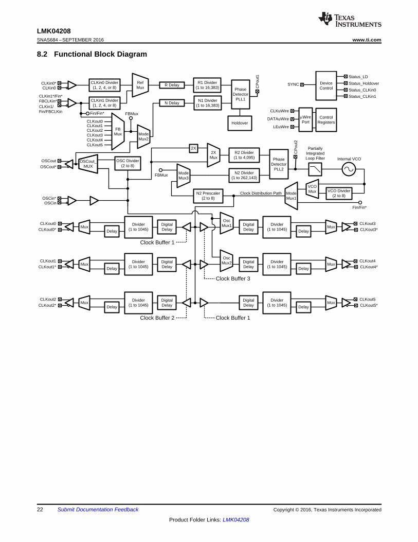
8.2 Functional Block Diagram
23
LMK04208www.ti.com SNAS684 –SEPTEMBER 2016
Product Folder Links: LMK04208
Submit Documentation FeedbackCopyright © 2016, Texas Instruments Incorporated
8.3 Feature Description
8.3.1 Inputs / Outputs
8.3.1.1 PLL1 Reference Inputs (CLKin0 and CLKin1)The reference clock inputs for PLL1 may be selected from either CLKin0 or CLKin1. The user has the capabilityto manually select one of the inputs or to configure an automatic switching mode of operation. See Input ClockSwitching for more info.
CLKin0 and CLKin1 have dividers which allow the device to switch between reference inputs of differentfrequencies automatically without needing to reprogram the PLL1 R divider. The CLKin pre-divider values are 1,2, 4, and 8.
CLKin1 input can alternatively be used for external feedback in 0-delay mode (FBCLKin) or for an external VCOinput port (Fin).
8.3.1.2 PLL2 OSCin / OSCin* PortThe feedback from the external oscillator being locked with PLL1 drives the OSCin/OSCin* pins. Internally thissignal is routed to the PLL1 N Divider and to the reference input for PLL2.
This input may be driven with either a single-ended or differential signal and must be AC coupled. If operated insingle ended mode, the unused input must be connected to GND with a 0.1-µF capacitor.
8.3.1.3 Crystal OscillatorThe internal circuitry of the OSCin port also supports the optional implementation of a crystal based oscillatorcircuit. A crystal, a varactor diode, and a small number of other external components may be used to implementthe oscillator. The internal oscillator circuit is enabled by setting the EN_PLL2_XTAL bit. See EN_PLL2_XTAL.
8.3.2 Input Clock SwitchingManual, pin select, and automatic are three different kinds clock input switching modes can be set with theCLKin_SELECT_MODE register.
Below is information about how the active input clock is selected and what causes a switching event in thevarious clock input selection modes.
8.3.2.1 Input Clock Switching - Manual ModeWhen CLKin_SELECT_MODE is 0 or 1 then CLKin0 or CLKin1 respectively is always selected as the activeinput clock. Manual mode will also override the EN_CLKinX bits such that the CLKinX buffer will operate even ifCLKinX is disabled with EN_CLKinX = 0.• Entering Holdover: If holdover mode is enabled, then holdover mode is entered if Digital lock detect of PLL1
goes low and DISABLE_DLD1_DET = 0.• Exiting Holdover: The active clock for automatic exit of holdover mode is the manually selected clock input.
24
LMK04208SNAS684 –SEPTEMBER 2016 www.ti.com
Product Folder Links: LMK04208
Submit Documentation Feedback Copyright © 2016, Texas Instruments Incorporated
Feature Description (continued)8.3.2.2 Input Clock Switching - Pin Select ModeWhen CLKin_SELECT_MODE is 3, the pins Status_CLKin0 and Status_CLKin1 select which clock input isactive.• Clock Switch Event: Pins: Changing the state of Status_CLKin0 or Status_CLKin1 pins causes an input
clock switch event.• Clock Switch Event: PLL1 DLD: To prevent PLL1 DLD high to low transition from causing a input clock
switch event and causing the device to enter holdover mode, disable the PLL1 DLD detect by settingDISABLE_DLD1_DET = 1. This is the preferred behavior for Pin Select Mode.
• Configuring Pin Select Mode:– The Status_CLKin0_TYPE must be programmed to an input value for the Status_CLKin0 pin to function
as an input for pin select mode.– The Status_CLKin1_TYPE must be programmed to an input value for the Status_CLKin1 pin to function
as an input for pin select mode.– If the Status_CLKinX_TYPE is set as output, the input value is considered 0.– The polarity of Status_CLKin1 and Status_CLKin0 input pins cannot be inverted with the CLKin_SEL_INV
bit.– Table 1 defines which input clock is active depending on Status_CLKin0 and Status_CLKin1 state.
Table 1. Active Clock Input - Pin Select ModeSTATUS_CLKin1 STATUS_CLKin0 ACTIVE CLOCK
0 0 CLKin00 1 CLKin11 0 Reserved1 1 Holdover
The pin select mode will override the EN_CLKinX bits such that the CLKinX buffer will operate even if CLKinX isdisabled with EN_CLKinX = 0. To switch as fast as possible, keep the clock input buffers enabled (EN_CLKinX =1) that could be switched to.
8.3.2.2.1 Pin Select Mode and Host
When in the pin select mode, the host can monitor conditions of the clocking system which could cause the hostto switch the active clock input. The LMK04208 device can also provide indicators on the Status_LD andStatus_HOLDOVER like DAC Rail, PLL1 DLD, PLL1 and PLL2 DLD which the host can use in determining whichclock input to use as active clock input.
8.3.2.2.2 Switch Event without Holdover
When an input clock switch event is triggered and holdover mode is disabled, the active clock input immediatelyswitches to the selected clock. When PLL1 is designed with a narrow loop bandwidth, the switching transient isminimized.
8.3.2.2.3 Switch Event with Holdover
When an input clock switch event is triggered and holdover mode is enabled, the device will enter holdover modeand remain in holdover until a holdover exit condition is met as described in Holdover Mode. Then the device willcomplete the reference switch to the pin selected clock input.
8.3.2.3 Input Clock Switching - Automatic ModeWhen CLKin_SELECT_MODE is 4, the active clock is selected in priority order of enabled clock inputs startingupon an input clock switch event. The priority order of the clocks is CLKin0 → CLKin1 → CLKin0, and so forth.
For a clock input to be eligible to be switched through, it must be enabled using EN_CLKinX.
25
LMK04208www.ti.com SNAS684 –SEPTEMBER 2016
Product Folder Links: LMK04208
Submit Documentation FeedbackCopyright © 2016, Texas Instruments Incorporated
(1) The polarity of Status_CLKin1 and Status_CLKin0 input pins can be inverted with the CLKin_SEL_INV bit.
8.3.2.3.1 Starting Active Clock
Upon programming this mode, the currently active clock remains active if PLL1 lock detect is high. To ensure aparticular clock input is the active clock when starting this mode, program CLKin_SELECT_MODE to the manualmode which selects the desired clock input (CLKin0 or 1). Wait for PLL1 to lock PLL1_DLD = 1, then select thismode with CLKin_SELECT_MODE = 4.
8.3.2.3.2 Clock Switch Event: PLL1 DLD
A loss of lock as indicated by PLL1’s DLD signal (PLL1_DLD = 0) will cause an input clock switch event ifDISABLE_DLD1_DET = 0. PLL1 DLD must go high (PLL1_DLD = 1) in between input clock switching events.
8.3.2.3.3 Clock Switch Event: PLL1 Vtune Rail
If Vtune_RAIL_DET_EN is set and the PLL1 Vtune voltage crosses the DAC high or low threshold, holdovermode will be entered. Since PLL1_DLD = 0 in holdover a clock input switching event will occur.
8.3.2.3.4 Clock Switch Event with Holdover
Clock switch event with holdover enabled is recommended in this input clock switching mode. When an inputclock switch event occurs, holdover mode is entered and the active clock is set to the clock input defined by theStatus_CLKinX pins. When the new active clock meets the holdover exit conditions, holdover is exited and theactive clock will continue to be used as a reference until another input clock switch event. PLL1 DLD must gohigh in between input clock switching events.
8.3.2.4 Input Clock Switching - Automatic Mode with Pin SelectWhen CLKin_SELECT_MODE is 6, the active clock is selected using the Status_CLKinX pins upon an inputclock switch event according to Table 2.
8.3.2.4.1 Starting Active Clock
Upon programming this mode, the currently active clock remains active if PLL1 lock detect is high. To ensure aparticular clock input is the active clock when starting this mode, program CLKin_SELECT_MODE to the manualmode which selects the desired clock input (CLKin0 or 1). Wait for PLL1 to lock PLL1_DLD = 1, then select thismode with CLKin_SELECT_MODE = 6.
8.3.2.4.2 Clock Switch Event: PLL1 DLD
An input clock switch event is generated by a loss of lock as indicated by PLL1's DLD signal (PLL1 DLD = 0).
8.3.2.4.3 Clock Switch Event: PLL1 Vtune Rail
If Vtune_RAIL_DET_EN is set and the PLL1 Vtune voltage crosses the DAC threshold, holdover mode will beentered. Since PLL1_DLD = 0 in holdover, a clock input switching event will occur.
8.3.2.4.4 Clock Switch Event with Holdover
Clock switch event with holdover enabled is recommended in this input clock switching mode. When an inputclock switch event occurs, holdover mode is entered and the active clock is set to the clock input defined by theStatus_CLKinX pins. When the new active clock meets the holdover exit conditions, holdover is exited and theactive clock will continue to be used as a reference until another input clock switch event. PLL1 DLD must gohigh in between input clock switching events."
Table 2. Active Clock Input - Auto Pin ModeSTATUS_CLKin1 (1) STATUS_CLKin0 ACTIVE CLOCK
X 1 CLKin01 0 CLKin10 0 Reserved
26
LMK04208SNAS684 –SEPTEMBER 2016 www.ti.com
Product Folder Links: LMK04208
Submit Documentation Feedback Copyright © 2016, Texas Instruments Incorporated
8.3.3 Holdover ModeHoldover mode causes PLL2 to stay locked on frequency with minimal frequency drift when an input clockreference to PLL1 becomes invalid. While in holdover mode, the PLL1 charge pump is TRI-STATED and a fixedtuning voltage is set on CPout1 to operate PLL1 in open loop.
8.3.3.1 Enable HoldoverProgram HOLDOVER_MODE to enable holdover mode. Holdover mode can be manually enabled byprogramming the FORCE_HOLDOVER bit.
The holdover mode can be set to operate in 2 different sub-modes.• Fixed CPout1 (EN_TRACK = 0 or 1, EN_MAN_DAC = 1).• Tracked CPout1 (EN_TRACK = 1, EN_MAN_DAC = 0).
– Not valid when EN_VTUNE_RAIL_DET = 1.
Updates to the DAC value for the Tracked CPout1 sub-mode occurs at the rate of the PLL1 phase detectorfrequency divided by DAC_CLK_DIV. These updates occur any time EN_TRACK = 1.
The DAC update rate should be programmed for <= 100 kHz to ensure DAC holdover accuracy.
When tracking is enabled the current voltage of DAC can be readback, see DAC_CNT.
8.3.3.2 Entering HoldoverThe holdover mode is entered as described in Input Clock Switching. Typically this is because:• FORCE_HOLDOVER bit is set.• PLL1 loses lock according to PLL1_DLD, and
– HOLDOVER_MODE = 2– DISABLE_DLD1_DET = 0
• CPout1 voltage crosses DAC high or low threshold, and– HOLDOVER_MODE = 2– EN_VTUNE_RAIL_DET = 1– EN_TRACK = 1– DAC_HIGH_TRIP = User Value– DAC_LOW_TRIP = User Value– EN_MAN_DAC = 1– MAN_DAC = User Value
8.3.3.3 During HoldoverPLL1 is run in open loop mode.• PLL1 charge pump is set to TRI-STATE.• PLL1 DLD will be unasserted.• The HOLDOVER status is asserted• During holdover If PLL2 was locked prior to entry of holdover mode, PLL2 DLD will continue to be asserted.• CPout1 voltage will be set to:
– a voltage set in the MAN_DAC register (fixed CPout1).– a voltage determined to be the last valid CPout1 voltage (tracked CPout1).
• PLL1 DLD will attempt to lock with the active clock input.
The HOLDOVER status signal can be monitored on the Status_HOLDOVER or Status_LD pin by programmingthe HOLDOVER_MUX or LD_MUX register to Holdover Status.
± ´ ´± =
6.4 mV 17 kHz / V 1e60.71ppm
153.6 MHz
Holdover accuracy (ppm) = ± 6.4 mV × Kv × 1e6
VCXO Frequency
27
LMK04208www.ti.com SNAS684 –SEPTEMBER 2016
Product Folder Links: LMK04208
Submit Documentation FeedbackCopyright © 2016, Texas Instruments Incorporated
8.3.3.4 Exiting HoldoverHoldover mode can be exited in one of two ways.• Manually, by programming the device from the host.• Automatically, By a clock operating within a specified ppm of the current PLL1 frequency on the active clock
input. See Input Clock Switching for more detail on which clock input is active.
To exit holdover by programming, set HOLDOVER_MODE = Disabled. HOLDOVER_MODE can then be re-enabled by programming HOLDOVER_MODE = Enabled. Care should be taken to ensure that the active clockupon exiting holdover is as expected, otherwise the CLKin_SELECT_MODE register may need to be re-programmed.
8.3.3.5 Holdover Frequency Accuracy and DAC PerformanceWhen in holdover mode, PLL1 runs in open loop and the DAC sets the CPout1 voltage. If Fixed CPout1 mode isused, then the output of the DAC is a voltage dependant upon the MAN_DAC register. If Tracked CPout1 modeis used, then the output of the DAC is the voltage at the CPout1 pin before holdover mode was entered. Whenusing Tracked mode and EN_MAN_DAC = 1, during holdover the DAC value is loaded with the programmedvalue in MAN_DAC, not the tracked value.
When in Tracked CPout1 mode, the DAC has a worst case tracking error of ±2 LSBs once PLL1 tuning voltage isacquired. The step size is approximately 3.2 mV; therefore, the VCXO frequency error during holdover modecaused by the DAC tracking accuracy is ±6.4 mV × Kv, where Kv is the tuning sensitivity of the VCXO in use.Therefore, the accuracy of the system when in holdover mode in ppm is:
(1)
Example: Consider a system with a 19.2-MHz clock input, a 153.6-MHz VCXO with a Kv of 17 kHz/V. Theaccuracy of the system in holdover in ppm is:
(2)
It is important to account for this frequency error when determining the allowable frequency error window tocause holdover mode to exit.
8.3.3.6 Holdover Mode - Automatic Exit of HoldoverThe LMK04208 device can be programmed to automatically exit holdover mode when the accuracy of thefrequency on the active clock input achieves a specified accuracy. The programmable variables includePLL1_WND_SIZE and DLD_HOLD_CNT.
See Digital Lock Detect Frequency Accuracy to calculate the register values to cause holdover to automaticallyexit upon reference signal recovery to within a user specified ppm error of the holdover frequency.
It is possible for the time to exit holdover to vary because the condition for automatic holdover exit is for thereference and feedback signals to have a time/phase error less than a programmable value. Because it ispossible for two clock signals to be very close in frequency but not close in phase, it may take a long time for thephases of the clocks to align themselves within the allowable time/phase error before holdover exits.
28
LMK04208SNAS684 –SEPTEMBER 2016 www.ti.com
Product Folder Links: LMK04208
Submit Documentation Feedback Copyright © 2016, Texas Instruments Incorporated
8.3.4 PLLs
8.3.4.1 PLL1The maximum phase detector frequency (fPD1) of PLL1 is 40 MHz. Since a narrow loop bandwidth should beused for PLL1, the need to operate at high phase detector rate to lower the in-band phase noise becomesunnecessary. The maximum values for the PLL1 R and N dividers is 16,383. Charge pump current ranges from100 to 1600 µA. PLL1 N divider may be driven by OSCin port through the OSCout_MUX output (default) or byinternal or external feedback as selected by Feedback Mux in 0-delay mode.
Low charge pump currents and phase detector frequencies aid design of low loop bandwidth loop filters withreasonably sized components to allow the VCXO or PLL2 to dominate phase noise inside of PLL2 loopbandwidth. High charge pump currents may be used by PLL1 when using VCXOs with leaky tuning voltageinputs to improve system performance.
8.3.4.2 PLL2PLL2's maximum phase detector frequency (fPD2) is 155 MHz. Operating at highest possible phase detector ratewill ensure low in-band phase noise for PLL2 which in turn produces lower total jitter. The in-band phase noisefrom the reference input and PLL is proportional to N2. The maximum value for the PLL2 R divider is 4,095. Themaximum value for the PLL2 N divider is 262,143. The N2 Prescaler in the total N feedback path can beprogrammed for values 2 to 8 (all divides even and odd). Charge pump current ranges from 100 to 3200 µA.
High charge pump currents help to widen the PLL2 loop bandwidth to optimize PLL2 performance.
8.3.4.2.1 PLL2 Frequency Doubler
The PLL2 reference input at the OSCin port may be routed through a frequency doubler before the PLL2 RDivider. The frequency doubler feature allows the phase comparison frequency to be increased when a relativelylow frequency oscillator is driving the OSCin port. By doubling the PLL2 phase detector frequency, the in-bandPLL2 noise is reduced by about 3 dB.
When using the doubler, PLL2 R Divider may be used to reduce the phase detector frequency to the limit of thePLL2 maximum phase detector frequency.
For applications in which the OSCin frequency and PLL2 phase detector frequency are equal, the best PLL2 in-band noise can be achieved when the doubler is enabled (EN_PLL2_REF_2X = 1) and the PLL2 R divide valueis 2. Do not use doubler disabled (EN_PLL2_REF_2X = 0) and PLL2 R divide value of 1.
PLLX Lock Count
PLLX_DLD_CNT
=Phase Error < g
NO
NO
NO
YESPhase Error < gSTART
PLLX
Lock Detected = False
Lock Count = 0
Increment
PLLX Lock Count
PLLX
Lock Detected = True
YES
YES
29
LMK04208www.ti.com SNAS684 –SEPTEMBER 2016
Product Folder Links: LMK04208
Submit Documentation FeedbackCopyright © 2016, Texas Instruments Incorporated
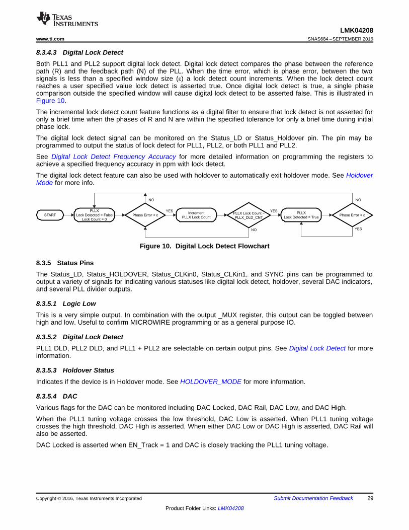
8.3.4.3 Digital Lock DetectBoth PLL1 and PLL2 support digital lock detect. Digital lock detect compares the phase between the referencepath (R) and the feedback path (N) of the PLL. When the time error, which is phase error, between the twosignals is less than a specified window size (ε) a lock detect count increments. When the lock detect countreaches a user specified value lock detect is asserted true. Once digital lock detect is true, a single phasecomparison outside the specified window will cause digital lock detect to be asserted false. This is illustrated inFigure 10.
The incremental lock detect count feature functions as a digital filter to ensure that lock detect is not asserted foronly a brief time when the phases of R and N are within the specified tolerance for only a brief time during initialphase lock.
The digital lock detect signal can be monitored on the Status_LD or Status_Holdover pin. The pin may beprogrammed to output the status of lock detect for PLL1, PLL2, or both PLL1 and PLL2.
See Digital Lock Detect Frequency Accuracy for more detailed information on programming the registers toachieve a specified frequency accuracy in ppm with lock detect.
The digital lock detect feature can also be used with holdover to automatically exit holdover mode. See HoldoverMode for more info.
Figure 10. Digital Lock Detect Flowchart
8.3.5 Status PinsThe Status_LD, Status_HOLDOVER, Status_CLKin0, Status_CLKin1, and SYNC pins can be programmed tooutput a variety of signals for indicating various statuses like digital lock detect, holdover, several DAC indicators,and several PLL divider outputs.
8.3.5.1 Logic LowThis is a very simple output. In combination with the output _MUX register, this output can be toggled betweenhigh and low. Useful to confirm MICROWIRE programming or as a general purpose IO.
8.3.5.2 Digital Lock DetectPLL1 DLD, PLL2 DLD, and PLL1 + PLL2 are selectable on certain output pins. See Digital Lock Detect for moreinformation.
8.3.5.3 Holdover StatusIndicates if the device is in Holdover mode. See HOLDOVER_MODE for more information.
8.3.5.4 DACVarious flags for the DAC can be monitored including DAC Locked, DAC Rail, DAC Low, and DAC High.
When the PLL1 tuning voltage crosses the low threshold, DAC Low is asserted. When PLL1 tuning voltagecrosses the high threshold, DAC High is asserted. When either DAC Low or DAC High is asserted, DAC Rail willalso be asserted.
DAC Locked is asserted when EN_Track = 1 and DAC is closely tracking the PLL1 tuning voltage.
30
LMK04208SNAS684 –SEPTEMBER 2016 www.ti.com
Product Folder Links: LMK04208
Submit Documentation Feedback Copyright © 2016, Texas Instruments Incorporated
8.3.5.5 PLL Divider OutputsThe PLL divider outputs are useful for debugging failure to lock issues. It allows the user to measure thefrequency the PLL inputs are receiving. The settings of PLL1_R, PLL1_N, PLL2_R, and PLL2_N output pulses atthe phase detector rate. The settings of PLL1_R / 2, PLL1_N / 2, PLL2_R / 2, and PLL2_N / 2 output a 50% dutycycle waveform at half the phase detector rate.
8.3.5.6 CLKinX_LOSThe clock input loss of signal indicator is asserted when LOS is enabled (EN_LOS) and the clock no longerdetects an input as defined by the time-out threshold, LOS_TIMEOUT.
8.3.5.7 CLKinX SelectedIf this clock is the currently selected/active clock, this pin will be asserted.
8.3.5.8 MICROWIRE ReadbackThe readback data can be output on any pin programmable to readback mode. For more information onreadback see Readback.
8.3.6 VCOThe integrated VCO uses a frequency calibration routine when register R30 is programmed to lock VCO to targetfrequency. Register R30 contains the PLL2_N register.
During the frequency calibration the PLL2_N_CAL value is used instead of PLL2_N, this allows 0-delay modes tohave a separate PLL2 N value for VCO frequency calibration and regular operation. See Register 29, Register30, and PLL Programming for more information.
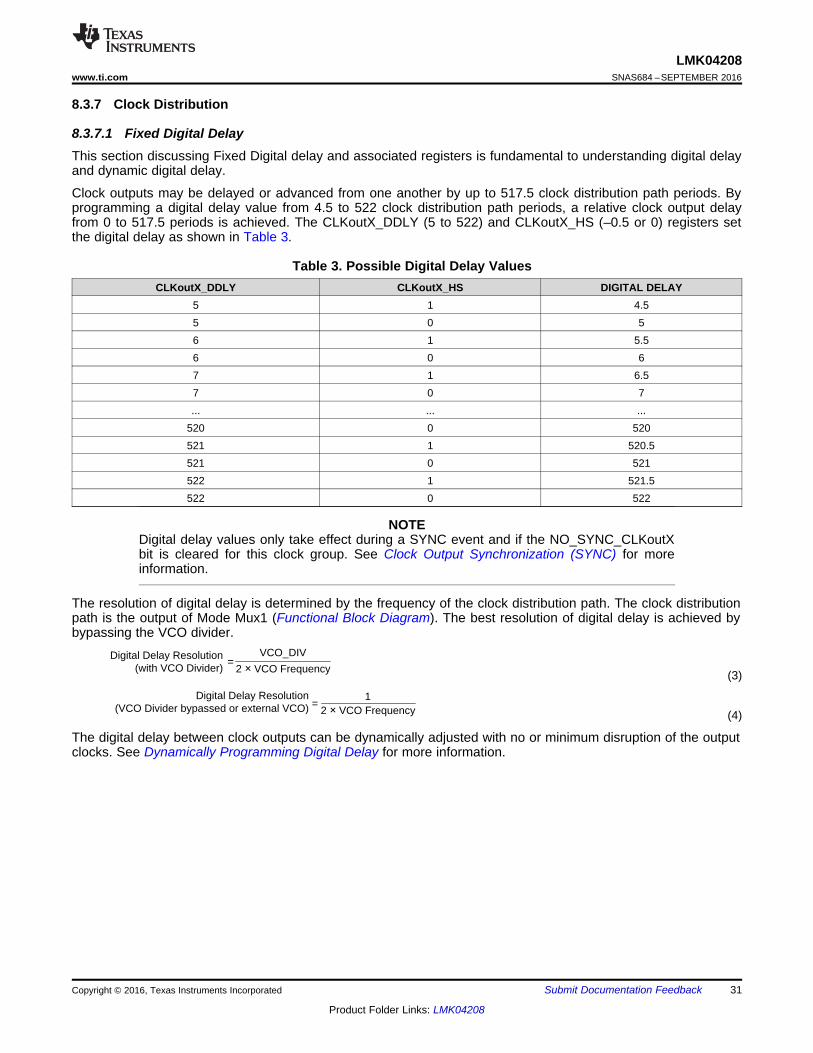
Digital Delay Resolution(VCO Divider bypassed or external VCO)
12 × VCO Frequency
=
Digital Delay Resolution(with VCO Divider)
VCO_DIV
2 × VCO Frequency=
31
LMK04208www.ti.com SNAS684 –SEPTEMBER 2016
Product Folder Links: LMK04208
Submit Documentation FeedbackCopyright © 2016, Texas Instruments Incorporated
8.3.7 Clock Distribution
8.3.7.1 Fixed Digital DelayThis section discussing Fixed Digital delay and associated registers is fundamental to understanding digital delayand dynamic digital delay.
Clock outputs may be delayed or advanced from one another by up to 517.5 clock distribution path periods. Byprogramming a digital delay value from 4.5 to 522 clock distribution path periods, a relative clock output delayfrom 0 to 517.5 periods is achieved. The CLKoutX_DDLY (5 to 522) and CLKoutX_HS (–0.5 or 0) registers setthe digital delay as shown in Table 3.
Table 3. Possible Digital Delay ValuesCLKoutX_DDLY CLKoutX_HS DIGITAL DELAY
5 1 4.55 0 56 1 5.56 0 67 1 6.57 0 7... ... ...
520 0 520521 1 520.5521 0 521522 1 521.5522 0 522
NOTEDigital delay values only take effect during a SYNC event and if the NO_SYNC_CLKoutXbit is cleared for this clock group. See Clock Output Synchronization (SYNC) for moreinformation.
The resolution of digital delay is determined by the frequency of the clock distribution path. The clock distributionpath is the output of Mode Mux1 (Functional Block Diagram). The best resolution of digital delay is achieved bybypassing the VCO divider.
(3)
(4)
The digital delay between clock outputs can be dynamically adjusted with no or minimum disruption of the outputclocks. See Dynamically Programming Digital Delay for more information.
32
LMK04208SNAS684 –SEPTEMBER 2016 www.ti.com
Product Folder Links: LMK04208
Submit Documentation Feedback Copyright © 2016, Texas Instruments Incorporated
(1) CLKout2_DDLY = 5 and CLKout2_HS = 0
8.3.7.2 Fixed Digital Delay - ExampleGiven a VCO frequency of 2949.12 MHz and no VCO divider, by using digital delay the outputs can be adjustedin 1 / (2 * 2949.12 MHz) = ~169.54 ps steps.
To achieve quadrature (90 degree shift) between the 122.88-MHz outputs on CLKout4 and CLKout6 from a VCOfrequency of 2949.12 MHz and bypassing the VCO divider, consider the following:1. The frequency of 122.88 MHz has a period of ~8.14 ns.2. To delay 90 degrees of a 122.88-MHz clock period requires a ~2.03 ns delay.3. Given a digital delay step of ~169.54 ps, this requires a digital delay value of 12 steps (2.03 ns / 169.54 ps =
12).4. Since the 12 steps are half period steps, CLKout3_DDLY is programmed 6 full periods beyond 5 for a total of
11.
This result in the following programming:• Clock output dividers to 24. CLKout2_DIV = 24 and CLKout3_DIV = 24.• Set first clock digital delay value. CLKout2_DDLY = 5, CLKout2_HS = 0.• Set second 90 degree shifted clock digital delay value. CLKout3_DDLY = 11, CLKout3_HS = 0.
Table 4 shows some of the possible phase delays in degrees achievable in the above example.
Table 4. Relative Phase Shift from CLKout4 and 5 to CLKout6 and 7 (1)
CLKout3_DDLY CLKout3_HS RELATIVE DIGITAL DELAY DEGREES of 122.88 MHz5 1 -0.5 -7.5°5 0 0.0 0°6 1 0.5 7.5°6 0 1.0 15.0°7 1 1.5 22.5°7 0 2.0 30.0°8 1 2.5 37.5°8 0 3.0 45.0°9 1 3.5 52.5°9 0 4.0 60.0°10 1 4.5 67.5°10 0 5.0 75.0°11 1 5.5 82.5°11 0 6.0 90.0°12 1 6.5 97.5°12 0 7.0 105.0°13 1 7.5 112.5°13 0 8.0 120.0°14 1 8.5 127.5°... ... ... ...
Figure 12 illustrates clock outputs programmed with different digital delay values during a SYNC event.
Refer to Dynamically Programming Digital Delay for more information on dynamically adjusting digital delay.
33
LMK04208www.ti.com SNAS684 –SEPTEMBER 2016
Product Folder Links: LMK04208
Submit Documentation FeedbackCopyright © 2016, Texas Instruments Incorporated
8.3.7.3 Clock Output Synchronization (SYNC)The purpose of the SYNC function is to synchronize the clock outputs with a fixed and known phase relationshipbetween each clock output selected for SYNC. SYNC can also be used to hold the outputs in a low or 0 state.The NO_SYNC_CLKoutX bits can be set to disable synchronization for a clock group.
To enable SYNC, EN_SYNC must be set. See EN_SYNC, Enable Synchronization.
The digital delay value set by CLKoutX_DDLY takes effect only upon a SYNC event. The digital delay due toCLKoutX_HS takes effect immediately upon programming. See Dynamically Programming Digital Delay for moreinformation on dynamically changing digital delay.
During a SYNC event, clock outputs driven by the VCO are not synchronized to clock outputs driven by OSCin.OSCout is always driven by OSCin. CLKout3 or CLKout4 may be driven by OSCin depending on theCLKoutX_OSCin_Sel bit value. While SYNC is asserted, NO_SYNC_CLKoutX operates normally for CLKout3 orCLKout4 under all circumstances. SYNC operates normally for CLKout3 or CLKout4 when driven by VCO.
8.3.7.3.1 Effect of SYNC
When SYNC is asserted, the outputs to be synchronized are held in a logic low state. When SYNC isunasserted, the clock outputs to be synchronized are activated and will transition to a high state simultaneouslywith one another except where different digital delay values have been programmed.
Refer to Dynamically Programming Digital Delay for SYNC functionality when SYNC_QUAL = 1.
Table 5. Steady State Clock Output Condition Given Specified InputsSYNC_TYPE SYNC_POL
_INVSYNC PIN CLOCK OUTPUT STATE
0,1,2 (Input) 0 0 Active0,1,2 (Input) 0 1 Low0,1,2 (Input) 1 0 Low0,1,2 (Input) 1 1 Active
3, 4, 5, 6 (Output) 0 0 or 1 Active3, 4, 5, 6 (Output) 1 0 or 1 Low
8.3.7.3.2 Methods of Generating SYNC
There are five methods to generate a SYNC event:• Manual:
– Asserting the SYNC pin according to the polarity set by SYNC_POL_INV.– Toggling the SYNC_POL_INV bit though MICROWIRE will cause a SYNC to be asserted.
• Automatic:– If PLL1_SYNC_DLD or PLL2_SYNC_DLD is set, the SYNC pin will be asserted while DLD (digital lock
detect) is false for PLL1 or PLL2 respectively.– Programming Register R30, which contains PLL2_N will generate a SYNC event when using the internal
VCO.– Programming Register R0 through R5 when SYNC_EN_AUTO = 1.
NOTEDue to the speed of the clock distribution path (as fast as ~325 ps period) and the slowslew rate of the SYNC, the exact VCO cycle at which the SYNC is asserted or unassertedby the SYNC is undefined. The timing diagrams show a sharp transition of the SYNC toclarify functionality.
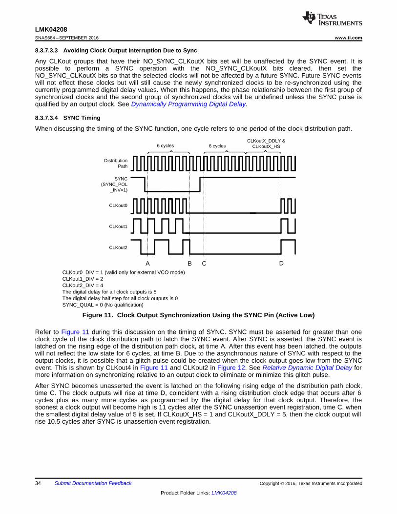
DistributionPath
SYNC(SYNC_POL
_INV=1)
CLKout0
CLKout1
CLKout2
A B C D
6 cycles 6 cyclesCLKoutX_DDLY &
CLKoutX_HS
34
LMK04208SNAS684 –SEPTEMBER 2016 www.ti.com
Product Folder Links: LMK04208
Submit Documentation Feedback Copyright © 2016, Texas Instruments Incorporated
8.3.7.3.3 Avoiding Clock Output Interruption Due to Sync
Any CLKout groups that have their NO_SYNC_CLKoutX bits set will be unaffected by the SYNC event. It ispossible to perform a SYNC operation with the NO_SYNC_CLKoutX bits cleared, then set theNO_SYNC_CLKoutX bits so that the selected clocks will not be affected by a future SYNC. Future SYNC eventswill not effect these clocks but will still cause the newly synchronized clocks to be re-synchronized using thecurrently programmed digital delay values. When this happens, the phase relationship between the first group ofsynchronized clocks and the second group of synchronized clocks will be undefined unless the SYNC pulse isqualified by an output clock. See Dynamically Programming Digital Delay.
8.3.7.3.4 SYNC Timing
When discussing the timing of the SYNC function, one cycle refers to one period of the clock distribution path.
CLKout0_DIV = 1 (valid only for external VCO mode)CLKout1_DIV = 2CLKout2_DIV = 4The digital delay for all clock outputs is 5The digital delay half step for all clock outputs is 0SYNC_QUAL = 0 (No qualification)
Figure 11. Clock Output Synchronization Using the SYNC Pin (Active Low)
Refer to Figure 11 during this discussion on the timing of SYNC. SYNC must be asserted for greater than oneclock cycle of the clock distribution path to latch the SYNC event. After SYNC is asserted, the SYNC event islatched on the rising edge of the distribution path clock, at time A. After this event has been latched, the outputswill not reflect the low state for 6 cycles, at time B. Due to the asynchronous nature of SYNC with respect to theoutput clocks, it is possible that a glitch pulse could be created when the clock output goes low from the SYNCevent. This is shown by CLKout4 in Figure 11 and CLKout2 in Figure 12. See Relative Dynamic Digital Delay formore information on synchronizing relative to an output clock to eliminate or minimize this glitch pulse.
After SYNC becomes unasserted the event is latched on the following rising edge of the distribution path clock,time C. The clock outputs will rise at time D, coincident with a rising distribution clock edge that occurs after 6cycles plus as many more cycles as programmed by the digital delay for that clock output. Therefore, thesoonest a clock output will become high is 11 cycles after the SYNC unassertion event registration, time C, whenthe smallest digital delay value of 5 is set. If CLKoutX_HS = 1 and CLKoutX_DDLY = 5, then the clock output willrise 10.5 cycles after SYNC is unassertion event registration.
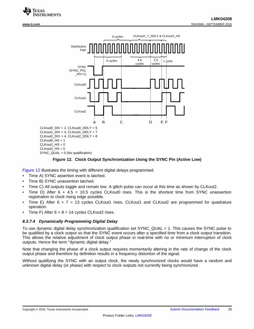
DistributionPath
SYNC(SYNC_POL
_INV=1)
CLKout0
CLKout1
CLKout2
A B C D E F
6 cycles
6 cycles
CLKoutX_Y_DDLY & CLKoutX_HS
4.5 cycles
2.5 cycles
1 cycle
35
LMK04208www.ti.com SNAS684 –SEPTEMBER 2016
Product Folder Links: LMK04208
Submit Documentation FeedbackCopyright © 2016, Texas Instruments Incorporated
CLKout0_DIV = 2, CLKout0_DDLY = 5CLKout1_DIV = 4, CLKout1_DDLY = 7CLKout2_DIV = 4, CLKout2_DDLY = 8CLKout0_HS = 1CLKout1_HS = 0CLKout2_HS = 0SYNC_QUAL = 0 (No qualification)
Figure 12. Clock Output Synchronization Using the SYNC Pin (Active Low)
Figure 12 illustrates the timing with different digital delays programmed.• Time A) SYNC assertion event is latched.• Time B) SYNC unassertion latched.• Time C) All outputs toggle and remain low. A glitch pulse can occur at this time as shown by CLKout2.• Time D) After 6 + 4.5 = 10.5 cycles CLKout0 rises. This is the shortest time from SYNC unassertion
registration to clock rising edge possible.• Time E) After 6 + 7 = 13 cycles CLKout1 rises. CLKout1 and CLKout2 are programmed for quadrature
operation.• Time F) After 6 + 8 = 14 cycles CLKout2 rises.
8.3.7.4 Dynamically Programming Digital DelayTo use dynamic digital delay synchronization qualification set SYNC_QUAL = 1. This causes the SYNC pulse tobe qualified by a clock output so that the SYNC event occurs after a specified time from a clock output transition.This allows the relative adjustment of clock output phase in real-time with no or minimum interruption of clockoutputs. Hence the term "dynamic digital delay."
Note that changing the phase of a clock output requires momentarily altering in the rate of change of the clockoutput phase and therefore by definition results in a frequency distortion of the signal.
Without qualifying the SYNC with an output clock, the newly synchronized clocks would have a random andunknown digital delay (or phase) with respect to clock outputs not currently being synchronized.
36
LMK04208SNAS684 –SEPTEMBER 2016 www.ti.com
Product Folder Links: LMK04208
Submit Documentation Feedback Copyright © 2016, Texas Instruments Incorporated
8.3.7.4.1 Absolute vs. Relative Dynamic Digital Delay
The clock used for qualification of SYNC is selected with the feedback mux (FEEDBACK_MUX).
If the clock selected by the feedback mux has its NO_SYNC_CLKoutX = 1, then an absolute dynamic digitaldelay adjustment will be performed during a SYNC event and the digital delay of the feedback clock will not beadjusted.
If the clock selected by the feedback mux has its NO_SYNC_CLKoutX = 0, then a self-referenced or relativedynamic digital delay adjustment will be performed during a SYNC event and the digital delay of the feedbackclock will be adjusted.
Clocks with NO_SYNC_CLKoutX = 1 always operate without interruption.
8.3.7.4.2 Dynamic Digital Delay and 0-Delay Mode
When using a 0-delay mode absolute dynamic digital delay is recommended. Using relative dynamic digitaldelay with a 0-delay mode may result in a momentary clock loss on the adjusted clock also being used for 0-delay feedback that may result in PLL1 DLD becoming low. This may result in HOLDOVER mode being activateddepending upon device configuration.
8.3.7.4.3 SYNC and Minimum Step Size
The minimum step size adjustment for digital delay is half a clock distribution path cycle. This is achieved byusing the CLKoutX_HS bit. The CLKoutX_HS bit change effect is immediate without the need for SYNC. To shiftdigital delay using CLKoutX_DDLY a SYNC signal must be generated for the change to take effect.
8.3.7.4.4 Programming Overview
To dynamically adjust the digital delay with respect to an existing clock output the device should be programmedas follows:• Set SYNC_QUAL = 1 for clock output qualification.• Set CLKout2_PD = 0. Required for proper operation of SYNC_QUAL = 1.• Set EN_FEEDBACK_MUX = 1 to enable the feedback buffer.• Set FEEDBACK_MUX to the clock output that the newly synchronized clocks will be qualified by.• Set NO_SYNC_CLKoutX = 1 for the output clocks that will continue to operate during the SYNC event. There
is no interruption of output on these clocks.– If FEEDBACK_MUX selects a clock output with NO_SYNC_CLKoutX = 1, then absolute dynamic digital
delay is performed.– If FEEDBACK_MUX selects a clock output with NO_SYNC_CLKoutX = 0, then self-referenced or relative
dynamic digital delay is performed.• The SYNC_EN_AUTO bit may be set to cause a SYNC event to begin when register R0 to R5 is
programmed. The auto SYNC feature is a convenience since does not require the application to manuallyassert SYNC by toggling the SYNC_POL_INV bit or the SYNC pin when changing digital delay. However,under the following condition a special programming sequence is required if SYNC_EN_AUTO = 1:– The CLKoutX_DDLY value being set in the programmed register is 13 or more.
• Under the following condition a SYNC_EN_AUTO must = 0:– If the application requires a digital delay resolution of half a clock distribution path cycle in relative
dynamic digital delay mode because the HS bit must be fixed per Table 6 for a qualifying clock.
8.3.7.4.5 Internal Dynamic Digital Delay Timing
To dynamically adjust digital delay a SYNC must occur. Once the SYNC is qualified by an output clock, 3 cycleslater an internal one shot pulse will occur. The width of the one shot pulse is 3 cycles. This internal one shotpulse will cause the outputs to turn off and then back on with a fixed delay with respect to the falling edge of thequalification clock. This allows for dynamic adjustments of digital delay with respect to an output clock.
The qualified SYNC timing is shown in Figure 13 for absolute dynamic digital delay and Figure 14 for relativedynamic digital delay.
37
LMK04208www.ti.com SNAS684 –SEPTEMBER 2016
Product Folder Links: LMK04208
Submit Documentation FeedbackCopyright © 2016, Texas Instruments Incorporated
8.3.7.4.6 Other Timing Requirements
When adjusting digital delay dynamically, the falling edge of the qualifying clock selected by theFEEDBACK_MUX must coincide with the falling edge of the clock distribution path. For this requirement to bemet, program the CLKoutX_HS value of the qualifying clock group according to Table 6.
Table 6. Half Step Programming Requirement of Qualifying Clock During Sync EventDISTRIBUTION PATH FREQUENCY CLKoutX_DIV VALUE CLKoutX_HS
≥ 1.8 GHzEven Must = 1 during SYNC event.Odd Must = 0 during SYNC event.
< 1.8 GHzEven Must = 0 during SYNC event.Odd Must = 1 during SYNC event.
8.3.7.5 Absolute Dynamic Digital DelayAbsolute dynamic digital delay can be used to program a clock output to a specific phase offset from anotherclock output.
Pros:• Simple direct phase adjustment with respect to another clock output.• CLKoutX_HS will remain constant for qualifying clock.
– Can easily use auto sync feature (SYNC_EN_AUTO = 1) when digital delay adjustment requires half stepdigital delay requirements.
• Can be used with 0-delay mode.
Cons:• For some phase adjustments there may be a glitch pulse due to SYNC assertion.
– For example, see CLKout4 in Figure 11 and CLKout2 in Figure 12.
8.3.7.5.1 Absolute Dynamic Digital Delay - Example
To illustrate the absolute dynamic digital delay adjust procedure, consider the following example.
System Requirements:• VCO Frequency = 2949.12 MHz• CLKout0 = 983.04 MHz (CLKout0_DIV = 3)• CLKout1 = 491.52 MHz (CLKout1_DIV = 6)• CLKout2 = 245.76 MHz (CLKout2_DIV = 12)• For all clock outputs during initial programming:
– CLKoutX_DDLY = 5– CLKoutX_HS = 1– NO_SYNC_CLKoutX = 0
The application requires the 491.52 MHz clock to be stepped in 30 degree steps (~169.5 ps), which is theminimum step resolution allowable by the clock distribution path requiring use of the half step bit (CLKoutX_HS).That is 1 / 2949.52 MHz / 2 = ~169.5 ps. During the stepping of the 491.52-MHz clock, the 983.04-MHz and245.76-MHz clock must not be interrupted.1. The device is programmed from register R0 to R30 with values that result in the device being locked and
operating as desired ( see the system requirements above). The phase of all the output clocks are alignedbecause all the digital delay and half step values were the same when the SYNC was generated byprogramming register R30. The timing of this is as shown in Figure 11.
2. Now the registers will be programmed to prepare for changing digital delay (or phase) dynamically.
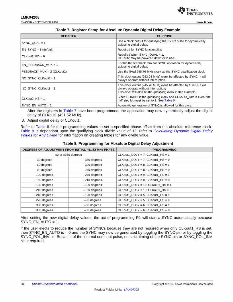
38
LMK04208SNAS684 –SEPTEMBER 2016 www.ti.com
Product Folder Links: LMK04208
Submit Documentation Feedback Copyright © 2016, Texas Instruments Incorporated
Table 7. Register Setup for Absolute Dynamic Digital Delay ExampleREGISTER PURPOSE
SYNC_QUAL = 1 Use a clock output for qualifying the SYNC pulse for dynamicallyadjusting digital delay.
EN_SYNC = 1 (default) Required for SYNC functionality.
CLKout2_PD = 0 Required when SYNC_QUAL = 1.CLKout2 may be powered down or in use.
EN_FEEDBACK_MUX = 1 Enable the feedback mux for SYNC operation for dynamicallyadjusting digital delay.
FEEDBACK_MUX = 2 (CLKout2) Use the fixed 245.76-MHz clock as the SYNC qualification clock.
NO_SYNC_CLKout0 = 1 This clock output (983.04 MHz) won't be affected by SYNC. It willalways operate without interruption.
NO_SYNC_CLKout2 = 1This clock output (245.76 MHz) won't be affected by SYNC. It willalways operate without interruption.This clock will also be the qualifying clock in this example.
CLKout2_HS = 1 Since CLKout2 is the qualifying clock and CLKoutX_DIV is even, thehalf step bit must be set to 1. See Table 6.
SYNC_EN_AUTO = 1 Automatic generation of SYNC is allowed for this case.
After the registers in Table 7 have been programmed, the application may now dynamically adjust the digitaldelay of CLKout1 (491.52 MHz).
3. Adjust digital delay of CLKout1.
Refer to Table 8 for the programming values to set a specified phase offset from the absolute reference clock.Table 8 is dependant upon the qualifying clock divide value of 12, refer to Calculating Dynamic Digital DelayValues for Any Divide for information on creating tables for any divide value.
Table 8. Programming for Absolute Digital Delay AdjustmentDEGREES OF ADJUSTMENT FROM INITIAL 491.52 MHz PHASE PROGRAMMING
±0 or ±360 degrees CLKout1_DDLY = 7; CLKout1_HS = 130 degrees –330 degrees CLKout1_DDLY = 7; CLKout1_HS = 060 degrees –300 degrees CLKout1_DDLY = 8; CLKout1_HS = 190 degrees –270 degrees CLKout1_DDLY = 8; CLKout1_HS = 0
120 degrees –240 degrees CLKout1_DDLY = 9; CLKout1_HS = 1150 degrees –210 degrees CLKout1_DDLY = 9; CLKout1_HS = 0180 degrees –180 degrees CLKout1_DDLY = 10; CLKout1_HS = 1210 degrees –150 degrees CLKout1_DDLY = 10; CLKout1_HS = 0240 degrees –120 degrees CLKout1_DDLY = 5; CLKout1_HS = 1270 degrees –90 degrees CLKout1_DDLY = 5; CLKout1_HS = 0300 degrees –60 degrees CLKout1_DDLY = 6; CLKout1_HS = 1330 degrees –30 degrees CLKout1_DDLY = 6; CLKout1_HS = 0
After setting the new digital delay values, the act of programming R1 will start a SYNC automatically becauseSYNC_EN_AUTO = 1.
If the user elects to reduce the number of SYNCs because they are not required when only CLKout1_HS is set,then SYNC_EN_AUTO is = 0 and the SYNC may now be generated by toggling the SYNC pin or by toggling theSYNC_POL_INV bit. Because of the internal one shot pulse, no strict timing of the SYNC pin or SYNC_POL_INVbit is required.
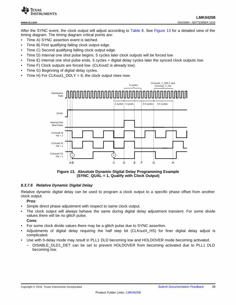
DistributionPath
Internal One Shot Pulse
5 cyclesCLKoutX_Y_DDLY and
CLKoutX_Y_HS
3 cycles
SYNC
5.5 cycles
AB C D E F G
CLKout0 /6HS = 1
CLKout2 /6HS = 1
CLKout4 /12HS = 1
3 cycles
H
5.5 cycles
21
39
LMK04208www.ti.com SNAS684 –SEPTEMBER 2016
Product Folder Links: LMK04208
Submit Documentation FeedbackCopyright © 2016, Texas Instruments Incorporated
After the SYNC event, the clock output will adjust according to Table 8. See Figure 13 for a detailed view of thetiming diagram. The timing diagram critical points are:• Time A) SYNC assertion event is latched.• Time B) First qualifying falling clock output edge.• Time C) Second qualifying falling clock output edge.• Time D) Internal one shot pulse begins. 5 cycles later clock outputs will be forced low• Time E) Internal one shot pulse ends. 5 cycles + digital delay cycles later the synced clock outputs rise.• Time F) Clock outputs are forced low. (CLKout2 is already low).• Time G) Beginning of digital delay cycles.• Time H) For CLKout1_DDLY = 6; the clock output rises now.
Figure 13. Absolute Dynamic Digital Delay Programming Example(SYNC_QUAL = 1, Qualify with Clock Output)
8.3.7.6 Relative Dynamic Digital DelayRelative dynamic digital delay can be used to program a clock output to a specific phase offset from anotherclock output.
Pros:• Simple direct phase adjustment with respect to same clock output.• The clock output will always behave the same during digital delay adjustment transient. For some divide
values there will be no glitch pulse.Cons:
• For some clock divide values there may be a glitch pulse due to SYNC assertion.• Adjustments of digital delay requiring the half step bit (CLKoutX_HS) for finer digital delay adjust is
complicated.• Use with 0-delay mode may result in PLL1 DLD becoming low and HOLDOVER mode becoming activated.
– DISABLE_DLD1_DET can be set to prevent HOLDOVER from becoming activated due to PLL1 DLDbecoming low.
40
LMK04208SNAS684 –SEPTEMBER 2016 www.ti.com
Product Folder Links: LMK04208
Submit Documentation Feedback Copyright © 2016, Texas Instruments Incorporated
8.3.7.6.1 Relative Dynamic Digital Delay - Example
To illustrate the relative dynamic digital delay adjust procedure, consider the following example.
System Requirements:• VCO Frequency = 2949.12 MHz• CLKout0 = 983.04 MHz (CLKout0_DIV = 3)• CLKout1 = 491.52 MHz (CLKout1_DIV = 6)• CLKout2 = 491.52 MHz (CLKout2_DIV = 6)• For all clock outputs during initial programming:
– CLKoutX_DDLY = 5– CLKoutX_HS = 0– NO_SYNC_CLKoutX = 0
The application requires the 491.52-MHz clock to be stepped in 30 degree steps (~169.5 ps), which is theminimum step resolution allowable by the clock distribution path. That is 1 / 2949.52 MHz / 2 = ~169.5 ps. Duringthe stepping of the 491.52 MHz clocks the 983.04 MHz clock must not be interrupted.1. The device is programmed from register R0 to R30 with values that result in the device being locked and
operating as desired, see the system requirements above. The phase of all the output clocks are alignedbecause all the digital delay and half step values were the same when the SYNC was generated byprogramming register R30. The timing of this is as shown in Figure 11.
2. Now the registers will be programmed to prepare for changing digital delay (or phase) dynamically.
Table 9. Register Setup for Relative Dynamic Digital Delay AdjustmentREGISTER PURPOSE
SYNC_QUAL = 1 Use clock output for qualifying the SYNC pulse for dynamically adjusting digital delay.EN_SYNC = 1 (default) Required for SYNC functionality.
CLKout2_PD = 0 Required when SYNC_QUAL = 1.CLKout4 and/or CLKout5 outputs may be powered down or in use.
EN_FEEDBACK_MUX = 1 Enable the feedback mux for SYNC operation for dynamically adjusting digital delay.FEEDBACK_MUX = 1 (CLKout1) Use the clock itself as the SYNC qualification clock.
NO_SYNC_CLKout0 = 1 This clock output (983.04 MHz) won't be affected by SYNC. It will always operate withoutinterruption.
NO_SYNC_CLKout2 = 1 CLKout3’s phase is not to change with respect to CLKout0.
SYNC_EN_AUTO = 0 (default)Automatic generation of SYNC is not allowed because of the half step requirement in relativedynamic digital delay mode.SYNC must be generated manually by toggling the SYNC_POL_INV bit or the SYNC pin.
After the above registers have been programmed, the application may now dynamically adjust the digitaldelay of the 491.52 MHz clocks.
3. Adjust digital delay of CLKout1 by one step which is 30 degrees or ~169.5 ps.
Refer to Table 10 for the programming sequence to step one half clock distribution period forward or backwards.Refer to Calculating Dynamic Digital Delay Values for Any Divide for more information on how to calculate digitaldelay and half step values for other cases.
To fulfill the qualifying clock output half step requirement in Table 6 when dynamically adjusting digital delay, theCLKoutX_HS bit must be cleared for clocks with even divides. So before any dynamic digital delay adjustment,CLKoutX_HS must be clear because the clock divide value is even. To achieve the final required digital delayadjustment, the CLKoutX_HS bit may set after SYNC.
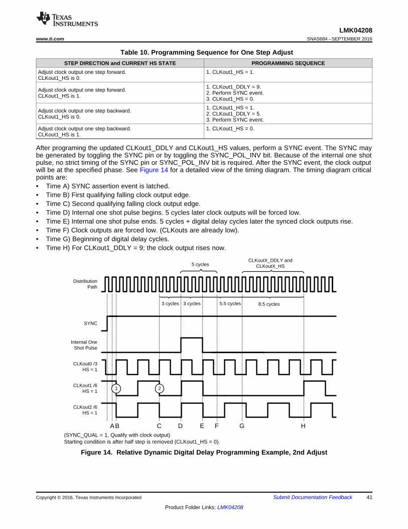
DistributionPath
Internal One Shot Pulse
5 cyclesCLKoutX_DDLY and
CLKoutX_HS
8.5 cycles3 cycles
SYNC
5.5 cycles
B C D E F G
CLKout0 /3HS = 1
CLKout1 /6HS = 1
CLKout2 /6HS = 1
3 cycles
2
HA
1
41
LMK04208www.ti.com SNAS684 –SEPTEMBER 2016
Product Folder Links: LMK04208
Submit Documentation FeedbackCopyright © 2016, Texas Instruments Incorporated
Table 10. Programming Sequence for One Step AdjustSTEP DIRECTION and CURRENT HS STATE PROGRAMMING SEQUENCE
Adjust clock output one step forward.CLKout1_HS is 0.
1. CLKout1_HS = 1.
Adjust clock output one step forward.CLKout1_HS is 1.
1. CLKout1_DDLY = 9.2. Perform SYNC event.3. CLKout1_HS = 0.
Adjust clock output one step backward.CLKout1_HS is 0.
1. CLKout1_HS = 1.2. CLKout1_DDLY = 5.3. Perform SYNC event.
Adjust clock output one step backward.CLKout1_HS is 1.
1. CLKout1_HS = 0.
After programing the updated CLKout1_DDLY and CLKout1_HS values, perform a SYNC event. The SYNC maybe generated by toggling the SYNC pin or by toggling the SYNC_POL_INV bit. Because of the internal one shotpulse, no strict timing of the SYNC pin or SYNC_POL_INV bit is required. After the SYNC event, the clock outputwill be at the specified phase. See Figure 14 for a detailed view of the timing diagram. The timing diagram criticalpoints are:• Time A) SYNC assertion event is latched.• Time B) First qualifying falling clock output edge.• Time C) Second qualifying falling clock output edge.• Time D) Internal one shot pulse begins. 5 cycles later clock outputs will be forced low.• Time E) Internal one shot pulse ends. 5 cycles + digital delay cycles later the synced clock outputs rise.• Time F) Clock outputs are forced low. (CLKouts are already low).• Time G) Beginning of digital delay cycles.• Time H) For CLKout1_DDLY = 9; the clock output rises now.
(SYNC_QUAL = 1, Qualify with clock output)Starting condition is after half step is removed (CLKout1_HS = 0).
Figure 14. Relative Dynamic Digital Delay Programming Example, 2nd Adjust
42
LMK04208SNAS684 –SEPTEMBER 2016 www.ti.com
Product Folder Links: LMK04208
Submit Documentation Feedback Copyright © 2016, Texas Instruments Incorporated
8.3.8 0-Delay ModeWhen 0-delay mode is enabled the clock output selected by the Feedback Mux is connected to the PLL1 Ncounter to ensure a fixed phase relationship between the selected CLKin and the fed back CLKout. When all theclock outputs are synced together, all the clock outputs will share the same fixed phase relationship between theselected CLKin and the fed back CLKout. The feedback can be internal or external using FBCLKin port.
When 0-delay mode is enabled the lowest frequency clock output is fed back to the Feedback Mux to ensure arepeatable fixed CLKin to CLKout phase relationship between all clock outputs.
If a clock output that is not the lowest frequency output is selected for feedback, then clocks with lowerfrequencies will have an unknown phase relationship with respect the other clocks and clock input. There will bea number of possible phase relationships equal to Feedback_Clock_Frequency / Lower_Clock_Frequency thatmay occur.
The Feedback Mux selects the even clock output of any clock group for internal feedback or the FBCLKin port forexternal 0-delay feedback. The even clock can remain powered down as long as the CLKoutX_PD bit is = 0 forits clock group.
To use 0-delay mode, the bit EN_FEEDBACK_MUX must be set (=1) to power up the feedback mux.
When using an external VCO mode, internal 0-delay feedback must be used since the FBCLKin port is sharedwith the Fin input.
See PLL Programming for more information on programming the various PLL and output dividers for 0-delaymode.
Table 11 outlines several registers to program for 0-delay mode.
Table 11. Programming 0-Delay ModeREGISTER PURPOSE
MODE = 2, 5, or 8
Select one of the 0-delay modes:Dual PLL, Internal VCODual PLL, External VCOSingle PLL, Internal VCO
EN_FEEDBACK_MUX = 1 Enable feedback mux.FEEDBACK_MUX = Application Specific Select CLKout or FBCLKin for 0-delay feedback.
CLKoutX_DIVThe divide value of the clock selected by FEEDBACK_MUX is important forPLL1_N or PLL2_N value calculation for Dual PLL or Single PLL moderespectively.
PLL1_N or PLL2_N PLL1_N or PLL2_N value used with CLKoutX_DIV in loop for Dual PLL or SinglePLL mode respectively.
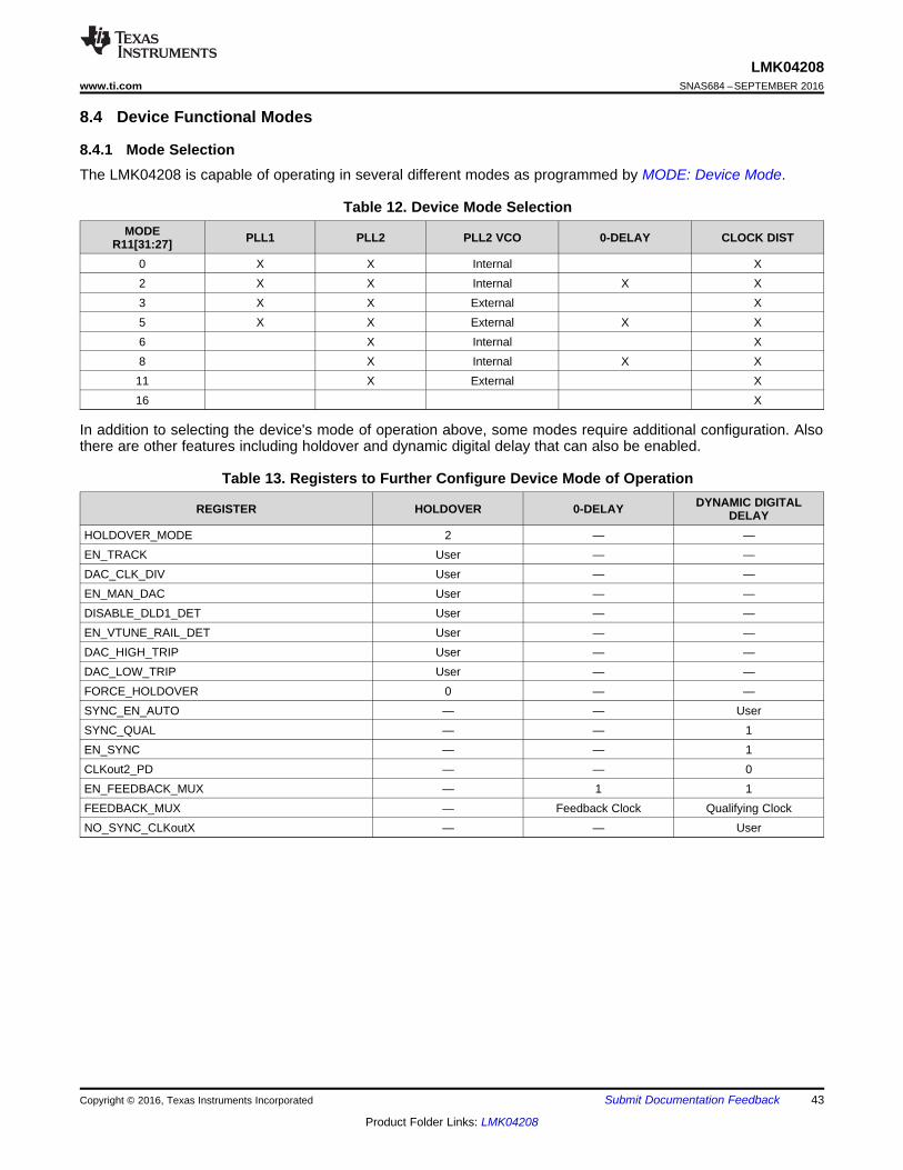
43
LMK04208www.ti.com SNAS684 –SEPTEMBER 2016
Product Folder Links: LMK04208
Submit Documentation FeedbackCopyright © 2016, Texas Instruments Incorporated
8.4 Device Functional Modes
8.4.1 Mode SelectionThe LMK04208 is capable of operating in several different modes as programmed by MODE: Device Mode.
Table 12. Device Mode SelectionMODE
R11[31:27] PLL1 PLL2 PLL2 VCO 0-DELAY CLOCK DIST
0 X X Internal X2 X X Internal X X3 X X External X5 X X External X X6 X Internal X8 X Internal X X11 X External X16 X
In addition to selecting the device's mode of operation above, some modes require additional configuration. Alsothere are other features including holdover and dynamic digital delay that can also be enabled.
Table 13. Registers to Further Configure Device Mode of Operation
REGISTER HOLDOVER 0-DELAY DYNAMIC DIGITALDELAY
HOLDOVER_MODE 2 — —EN_TRACK User — —DAC_CLK_DIV User — —EN_MAN_DAC User — —DISABLE_DLD1_DET User — —EN_VTUNE_RAIL_DET User — —DAC_HIGH_TRIP User — —DAC_LOW_TRIP User — —FORCE_HOLDOVER 0 — —SYNC_EN_AUTO — — UserSYNC_QUAL — — 1EN_SYNC — — 1CLKout2_PD — — 0EN_FEEDBACK_MUX — 1 1FEEDBACK_MUX — Feedback Clock Qualifying ClockNO_SYNC_CLKoutX — — User
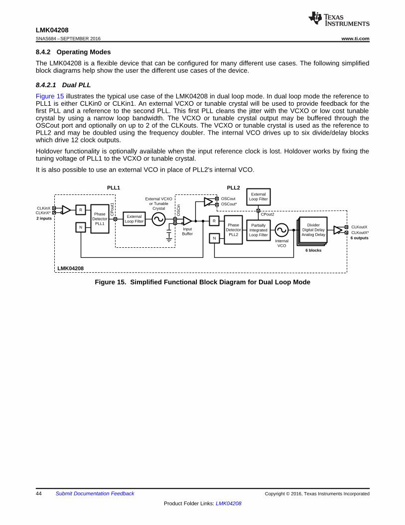
RCLKinXCLKinX*
N
Phase Detector
PLL1
External VCXO or Tunable
Crystal
R
N
Phase Detector
PLL2
InternalVCO
ExternalLoop Filter
OS
Cin
CP
out1
OSCoutOSCout*
LMK04208
CPout2
Partially Integrated Loop Filter
6 outputs
External Loop Filter
PLL1 PLL2
6 blocks
2 inputs
Input Buffer
CLKoutXCLKoutX*
Divider
Digital DelayAnalog Delay
44
LMK04208SNAS684 –SEPTEMBER 2016 www.ti.com
Product Folder Links: LMK04208
Submit Documentation Feedback Copyright © 2016, Texas Instruments Incorporated
8.4.2 Operating ModesThe LMK04208 is a flexible device that can be configured for many different use cases. The following simplifiedblock diagrams help show the user the different use cases of the device.
8.4.2.1 Dual PLLFigure 15 illustrates the typical use case of the LMK04208 in dual loop mode. In dual loop mode the reference toPLL1 is either CLKin0 or CLKin1. An external VCXO or tunable crystal will be used to provide feedback for thefirst PLL and a reference to the second PLL. This first PLL cleans the jitter with the VCXO or low cost tunablecrystal by using a narrow loop bandwidth. The VCXO or tunable crystal output may be buffered through theOSCout port and optionally on up to 2 of the CLKouts. The VCXO or tunable crystal is used as the reference toPLL2 and may be doubled using the frequency doubler. The internal VCO drives up to six divide/delay blockswhich drive 12 clock outputs.
Holdover functionality is optionally available when the input reference clock is lost. Holdover works by fixing thetuning voltage of PLL1 to the VCXO or tunable crystal.
It is also possible to use an external VCO in place of PLL2's internal VCO.
Figure 15. Simplified Functional Block Diagram for Dual Loop Mode
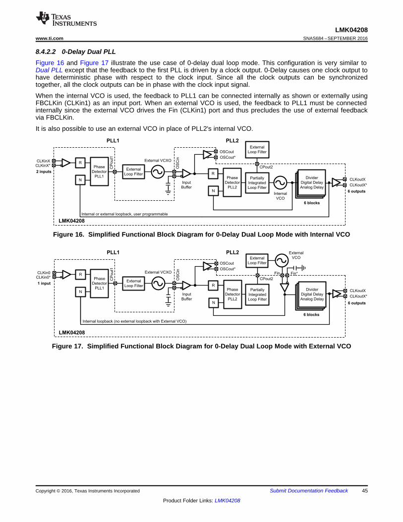
RCLKin0CLKin0* Phase
Detector
PLL1
External VCXO
R
N
Phase
Detector
PLL2
External
VCO
External
Loop Filter
Input
Buffer
CP
out1
OSCout
LMK04208
CPout2
Divider
Digital Delay
Analog Delay
CLKoutX
CLKoutX*
Partially
Integrated
Loop Filter6 outputs
PLL1 PLL2
6 blocks
1 input
N
OS
Cin
Internal loopback (no external loopback with External VCO)
Fin Fin*
External
Loop Filter
OSCout*
RCLKinXCLKinX* Phase
Detector
PLL1
External VCXO
R
N
Phase
Detector
PLL2
Internal
VCO
External
Loop Filter
Input
Buffer
CP
out1
OSCout
LMK04208
CPout2
Divider
Digital Delay
Analog Delay
CLKoutX
CLKoutX*
Partially
Integrated
Loop Filter6 outputs
External
Loop Filter
PLL1 PLL2
6 blocks
2 inputs
NO
SC
in
Internal or external loopback, user programmable
OSCout*
45
LMK04208www.ti.com SNAS684 –SEPTEMBER 2016
Product Folder Links: LMK04208
Submit Documentation FeedbackCopyright © 2016, Texas Instruments Incorporated
8.4.2.2 0-Delay Dual PLLFigure 16 and Figure 17 illustrate the use case of 0-delay dual loop mode. This configuration is very similar toDual PLL except that the feedback to the first PLL is driven by a clock output. 0-Delay causes one clock output tohave deterministic phase with respect to the clock input. Since all the clock outputs can be synchronizedtogether, all the clock outputs can be in phase with the clock input signal.
When the internal VCO is used, the feedback to PLL1 can be connected internally as shown or externally usingFBCLKin (CLKin1) as an input port. When an external VCO is used, the feedback to PLL1 must be connectedinternally since the external VCO drives the Fin (CLKin1) port and thus precludes the use of external feedbackvia FBCLKin.
It is also possible to use an external VCO in place of PLL2's internal VCO.
Figure 16. Simplified Functional Block Diagram for 0-Delay Dual Loop Mode with Internal VCO
Figure 17. Simplified Functional Block Diagram for 0-Delay Dual Loop Mode with External VCO
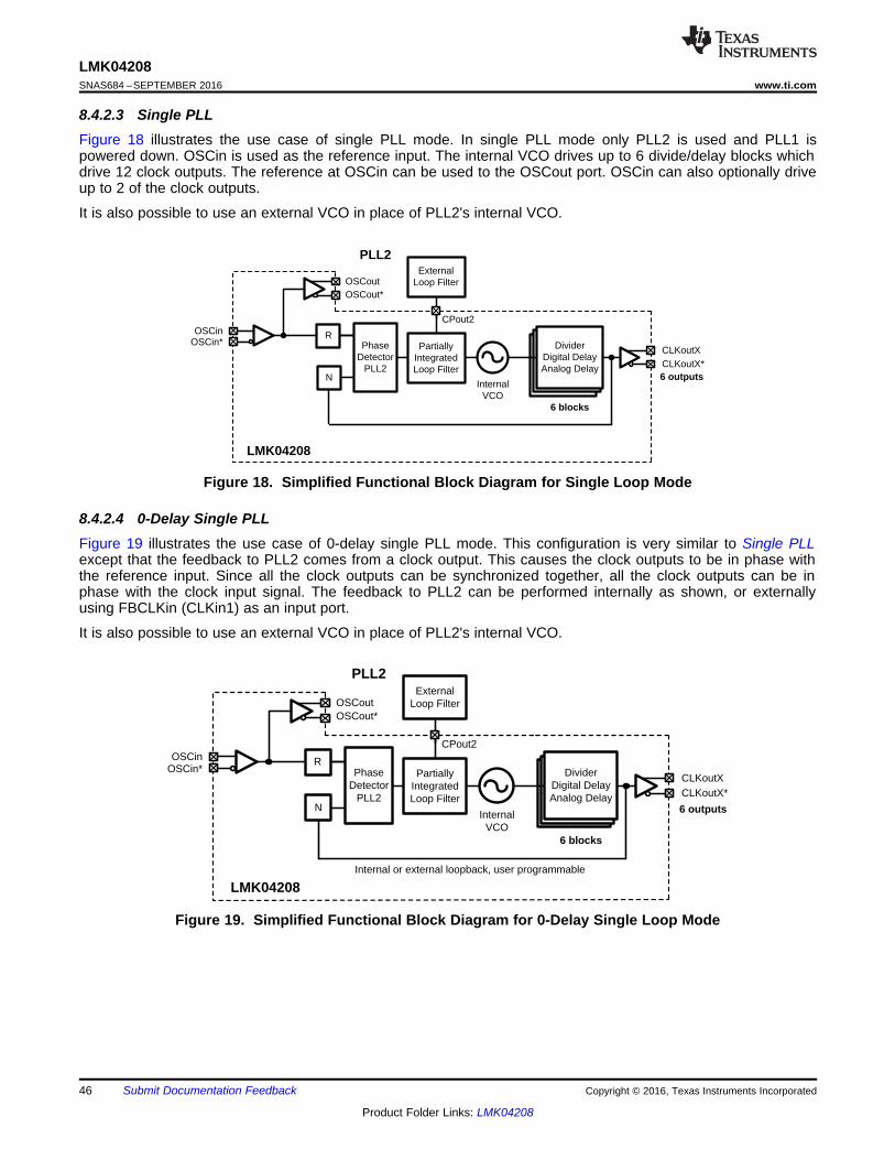
R
N
Phase Detector
PLL2
InternalVCO
OSCin
OSCoutOSCout*
LMK04208
CPout2
DividerDigital DelayAnalog Delay
CLKoutXCLKoutX*
Partially
Integrated Loop Filter
6 outputs
External Loop Filter
PLL2
6 blocks
OSCin*
Internal or external loopback, user programmable
R
N
Phase Detector
PLL2
InternalVCO
OSCin
OSCoutOSCout*
LMK04208
CPout2
Partially Integrated Loop Filter
6 outputs
External Loop Filter
PLL2
6 blocks
OSCin*CLKoutXCLKoutX*
Divider
Digital DelayAnalog Delay
46
LMK04208SNAS684 –SEPTEMBER 2016 www.ti.com
Product Folder Links: LMK04208
Submit Documentation Feedback Copyright © 2016, Texas Instruments Incorporated
8.4.2.3 Single PLLFigure 18 illustrates the use case of single PLL mode. In single PLL mode only PLL2 is used and PLL1 ispowered down. OSCin is used as the reference input. The internal VCO drives up to 6 divide/delay blocks whichdrive 12 clock outputs. The reference at OSCin can be used to the OSCout port. OSCin can also optionally driveup to 2 of the clock outputs.
It is also possible to use an external VCO in place of PLL2's internal VCO.
Figure 18. Simplified Functional Block Diagram for Single Loop Mode
8.4.2.4 0-Delay Single PLLFigure 19 illustrates the use case of 0-delay single PLL mode. This configuration is very similar to Single PLLexcept that the feedback to PLL2 comes from a clock output. This causes the clock outputs to be in phase withthe reference input. Since all the clock outputs can be synchronized together, all the clock outputs can be inphase with the clock input signal. The feedback to PLL2 can be performed internally as shown, or externallyusing FBCLKin (CLKin1) as an input port.
It is also possible to use an external VCO in place of PLL2's internal VCO.
Figure 19. Simplified Functional Block Diagram for 0-Delay Single Loop Mode
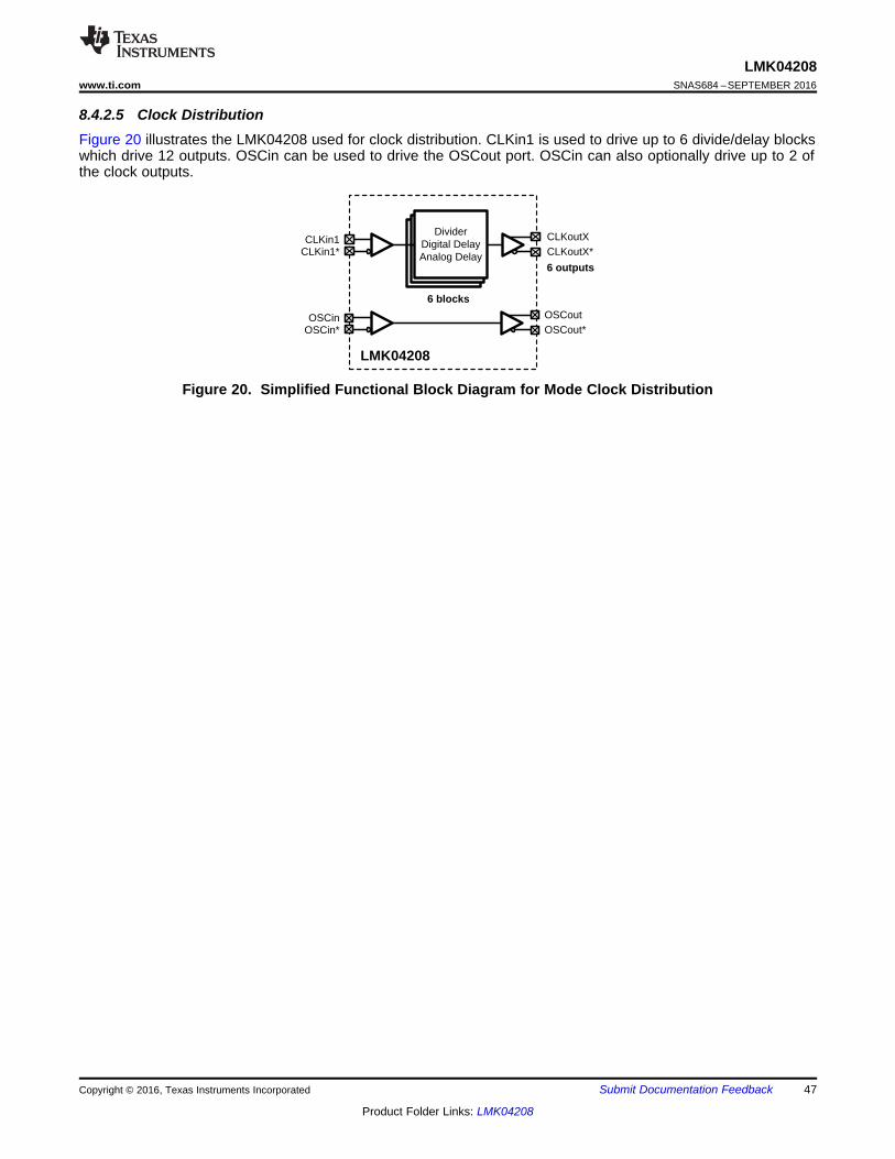
CLKin1CLKin1*
OSCin
OSCoutOSCout*
LMK04208
OSCin*
6 outputs
6 blocks
CLKoutXCLKoutX*
Divider
Digital DelayAnalog Delay
47
LMK04208www.ti.com SNAS684 –SEPTEMBER 2016
Product Folder Links: LMK04208
Submit Documentation FeedbackCopyright © 2016, Texas Instruments Incorporated
8.4.2.5 Clock DistributionFigure 20 illustrates the LMK04208 used for clock distribution. CLKin1 is used to drive up to 6 divide/delay blockswhich drive 12 outputs. OSCin can be used to drive the OSCout port. OSCin can also optionally drive up to 2 ofthe clock outputs.
Figure 20. Simplified Functional Block Diagram for Mode Clock Distribution
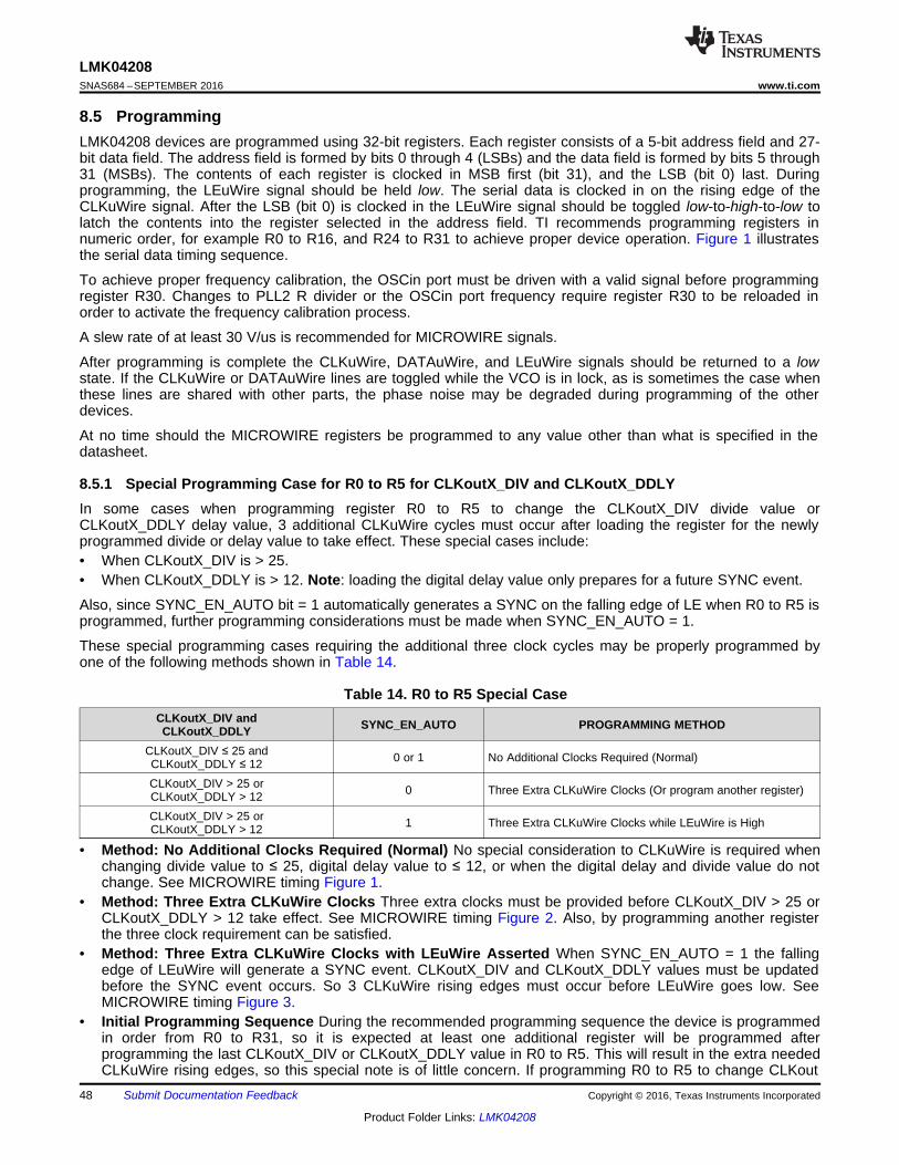
48
LMK04208SNAS684 –SEPTEMBER 2016 www.ti.com
Product Folder Links: LMK04208
Submit Documentation Feedback Copyright © 2016, Texas Instruments Incorporated
8.5 ProgrammingLMK04208 devices are programmed using 32-bit registers. Each register consists of a 5-bit address field and 27-bit data field. The address field is formed by bits 0 through 4 (LSBs) and the data field is formed by bits 5 through31 (MSBs). The contents of each register is clocked in MSB first (bit 31), and the LSB (bit 0) last. Duringprogramming, the LEuWire signal should be held low. The serial data is clocked in on the rising edge of theCLKuWire signal. After the LSB (bit 0) is clocked in the LEuWire signal should be toggled low-to-high-to-low tolatch the contents into the register selected in the address field. TI recommends programming registers innumeric order, for example R0 to R16, and R24 to R31 to achieve proper device operation. Figure 1 illustratesthe serial data timing sequence.
To achieve proper frequency calibration, the OSCin port must be driven with a valid signal before programmingregister R30. Changes to PLL2 R divider or the OSCin port frequency require register R30 to be reloaded inorder to activate the frequency calibration process.
A slew rate of at least 30 V/us is recommended for MICROWIRE signals.
After programming is complete the CLKuWire, DATAuWire, and LEuWire signals should be returned to a lowstate. If the CLKuWire or DATAuWire lines are toggled while the VCO is in lock, as is sometimes the case whenthese lines are shared with other parts, the phase noise may be degraded during programming of the otherdevices.
At no time should the MICROWIRE registers be programmed to any value other than what is specified in thedatasheet.
8.5.1 Special Programming Case for R0 to R5 for CLKoutX_DIV and CLKoutX_DDLYIn some cases when programming register R0 to R5 to change the CLKoutX_DIV divide value orCLKoutX_DDLY delay value, 3 additional CLKuWire cycles must occur after loading the register for the newlyprogrammed divide or delay value to take effect. These special cases include:• When CLKoutX_DIV is > 25.• When CLKoutX_DDLY is > 12. Note: loading the digital delay value only prepares for a future SYNC event.
Also, since SYNC_EN_AUTO bit = 1 automatically generates a SYNC on the falling edge of LE when R0 to R5 isprogrammed, further programming considerations must be made when SYNC_EN_AUTO = 1.
These special programming cases requiring the additional three clock cycles may be properly programmed byone of the following methods shown in Table 14.
Table 14. R0 to R5 Special CaseCLKoutX_DIV andCLKoutX_DDLY SYNC_EN_AUTO PROGRAMMING METHOD
CLKoutX_DIV ≤ 25 andCLKoutX_DDLY ≤ 12 0 or 1 No Additional Clocks Required (Normal)
CLKoutX_DIV > 25 orCLKoutX_DDLY > 12 0 Three Extra CLKuWire Clocks (Or program another register)
CLKoutX_DIV > 25 orCLKoutX_DDLY > 12 1 Three Extra CLKuWire Clocks while LEuWire is High
• Method: No Additional Clocks Required (Normal) No special consideration to CLKuWire is required whenchanging divide value to ≤ 25, digital delay value to ≤ 12, or when the digital delay and divide value do notchange. See MICROWIRE timing Figure 1.
• Method: Three Extra CLKuWire Clocks Three extra clocks must be provided before CLKoutX_DIV > 25 orCLKoutX_DDLY > 12 take effect. See MICROWIRE timing Figure 2. Also, by programming another registerthe three clock requirement can be satisfied.
• Method: Three Extra CLKuWire Clocks with LEuWire Asserted When SYNC_EN_AUTO = 1 the fallingedge of LEuWire will generate a SYNC event. CLKoutX_DIV and CLKoutX_DDLY values must be updatedbefore the SYNC event occurs. So 3 CLKuWire rising edges must occur before LEuWire goes low. SeeMICROWIRE timing Figure 3.
• Initial Programming Sequence During the recommended programming sequence the device is programmedin order from R0 to R31, so it is expected at least one additional register will be programmed afterprogramming the last CLKoutX_DIV or CLKoutX_DDLY value in R0 to R5. This will result in the extra neededCLKuWire rising edges, so this special note is of little concern. If programming R0 to R5 to change CLKout
49
LMK04208www.ti.com SNAS684 –SEPTEMBER 2016
Product Folder Links: LMK04208
Submit Documentation FeedbackCopyright © 2016, Texas Instruments Incorporated
frequency or digital delay or dynamic digital delay at a later time in the application, take care to provide theseextra CLKuWire cycles to properly load the new divide and/or delay values.
8.5.1.1 ExampleIn this example, all registers have been programmed, the PLLs are locked. An LMK04208 has been generating aclock output frequency of 61.44 MHz on CLKout4 using a VCO frequency of 2949.12 MHz and a divide value of48. SYNC_EN_AUTO = 0. At a later time the application requires a 30.72-MHz output on CLKout4. Byreprogramming register R4 with CLKout4_DIV = 96 twice, the divide value of 96 is set for clock output 4 whichresults in an output frequency of 30.72 MHz (2949.12 MHz / 96 = 30.72 MHz) on CLKout4.
In this example, the required 3 CLKuWire cycles were achieved by reprogramming the R4 register with the samevalue twice.
8.5.2 Recommended Programming SequenceRegisters are programmed in numeric order with R0 being the first and R31 being the last register programmed.The recommended programming sequence involves programming R0 with the reset bit (b17) set to 1 to ensurethe device is in a default state. If R0 is programmed again, the reset bit must be cleared to 0 during theprogramming of R0.
8.5.2.1 Programming Sequence Overview• Program R0 with RESET bit = 1. This ensures that the device is configured with default settings. When
RESET = 1, all other R0 bits are ignored.– If R0 is programmed again during the initial configuration of the device, the RESET bit must be cleared.
• R0 through R5: CLKouts.– Program as necessary to configure the clock outputs, CLKout0 to CLKout5 as desired. These registers
configure clock output controls such as powerdown, digital delay and divider value, analog delay select,and clock source select.
• R6 through R8: CLKouts.– Program as necessary to configure the clock outputs, CLKout0 to CLKout5 as desired. These registers
configure the output format for each clock output and the analog delay for the clock output groups.• R9: Required programming
– Program this register as shown in the register map for proper operation.• R10: OSCout, VCO divider, and 0-delay.
– Enable and configure clock outputs OSCout.– Set and select VCO divider (VCO bypass is recommended).– Set 0-delay feedback source if used.
• R11: Part mode, SYNC, and XTAL.– Program to configure the mode of the part, to configure SYNC functionality and pin, and to enable crystal
mode.• R12: Pins, SYNC, and holdover mode.
– Status_LD pin, more SYNC options to generate a SYNC upon PLL1 and/or PLL2 lock detect.– Enable clock features such as holdover.
• R13: Pins, holdover mode, and CLKins.– Status_HOLDOVER, Status_CLKin0, and Status_CLKin1 pin controls.– Enable clock inputs for use in specific part modes.
• R14: Pins, LOS, CLKins, and DAC.– Status_CLKin1 pin control.– Loss of signal detection, CLKin type, DAC rail detect enable and high and low trip points.
• R15: DAC and holdover mode.– Program to enable and set the manual DAC value.– HOLDOVER mode options.
• R16: Crystal amplitude.– Increasing XTAL_LVL can improve tunable crystal phase noise performance.
50
LMK04208SNAS684 –SEPTEMBER 2016 www.ti.com
Product Folder Links: LMK04208
Submit Documentation Feedback Copyright © 2016, Texas Instruments Incorporated
• R24: PLL1 and PLL2.– PLL1 N and R delay and PLL1 digital lock delay value.– PLL2 integrated loop filter.
• R25: DAC and PLL1.– Program to configure DAC update clock divider and PLL1 digital lock detect count.
• R26: PLL2.– Program to configure PLL2 options.
• R27: CLKins and PLL1.– Clock input pre-dividers.– Program to configure PLL1 options.
• R28: PLL1 and PLL2.– Program to configure PLL2 R and PLL1 N.
• R29: OSCin and PLL2.– Program to configure oscillator input frequency, PLL2 fast phase detector frequency mode, and PLL2 N
calibration value.• R30: PLL2.
– Program to configure PLL2 prescaler and PLL2 N value.• R31: uWire lock.
– Program to set the uWire_LOCK bit.
51
LMK04208www.ti.com SNAS684 –SEPTEMBER 2016
Product Folder Links: LMK04208
Submit Documentation FeedbackCopyright © 2016, Texas Instruments Incorporated
8.5.3 ReadbackReadback from the MICROWIRE programming registers is available. The MICROWIRE readback function canbe enabled on the Status_LD, Status_HOLDOVER, Status_CLKin0, Status_CLKin1, or SYNC pin byprogramming the corresponding MUX register to “uWire Readback” and the corresponding TYPE register to"Output (push-pull)." Power on reset defaults the Status_HOLDOVER pin to “uWire Readback.”
For timing specifications, see Timing Requirements. Figure 4 shows timing for LEuWire for both READBACK_LE= 1 and 0. The rising edges of CLKuWire during MICROWIRE readback continue to clock data on DATAuWireinto the device during readback. If after the readback, LEuWire transitions from low to high, this data will belatched to the decoded register. The decoded register address consists of the last 5 bits clocked on DATAuWireas shown in Figure 4.
NOTEFor debug of the MICROWIRE interface, TI recommends simply programming an outputpin mux to active low and then toggle the output type register between output andinverting output while observing the output pin for a low to high transition. For example, toverify MICROWIRE programming, set the LD_MUX = 0 (Low) and then toggle theLD_TYPE register between 3 (Output, push-pull) and 4 (Output inverted, push-pull). Theresult will be that the Status_LD pin will toggle from low to high.
To perform a readback operation first set the register to be read back by programming the READBACK_ADDRregister. Then after any MICROWIRE write operation, with the LEuWire pin held low continue to clock theCLKuWire pin. On every rising edge of the CLKuWire pin a new data bit is clocked onto the any pinsprogrammed for uWire Readback. If the READBACK_LE bit is set, the LEuWire pin should be left high afterLEuWire rising edge while continuing to clock the CLKuWire pin.
It is allowable to perform a register read back in the same MICROWIRE operation which set theREADBACK_ADDR register value.
Figure 4 illustrates the serial data timing sequence for a readback operation for both cases of READBACK_LE =0 (POR default) and READBACK_LE = 1.
Data is clocked out MSB first. After 27 clocks all the data values will have been read and the read operation iscomplete. If READBACK_LE = 1, the LEuWire line may now be lowered. It is allowable for the CLKuWire pin tobe clocked additional cycles, but the data on the readback pin will be invalid. CLKuWire must be low before thefalling edge of LEuWire.
8.5.3.1 Readback - ExampleTo readback register R3 perform the following steps:• Write R31 with READBACK_ADDR = 3; READBACK_LE = 0. DATAuWire and CLKuWire are toggled as
shown in Figure 1 with new data being clocked in on rising edges of CLKuWire• Toggle LEuWire high and then low as shown in Figure 1 and Figure 4. LEuWire is returned low because
READBACK_LE = 0.• Toggle CLKuWire high and then low 27 times to read back all 27 bits of register R3. Data is read MSB first.
Data is valid on falling edge of CLKuWire.• Read operation is complete.
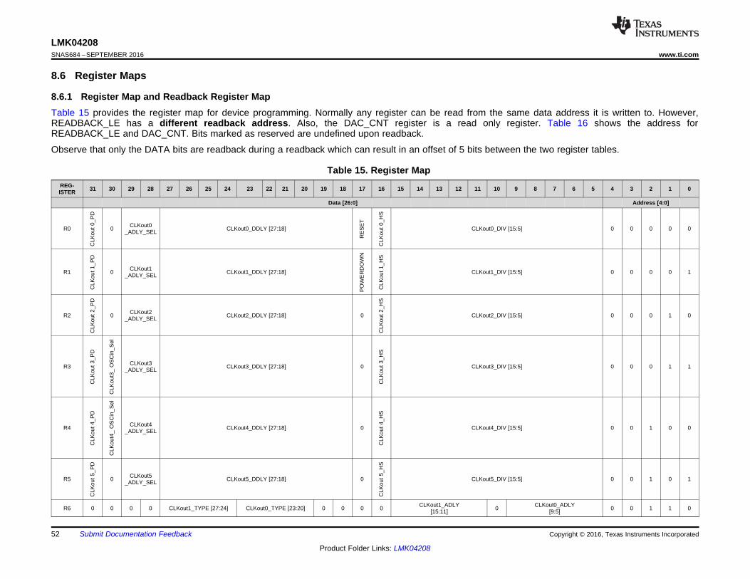
LMK04208SNAS684 –SEPTEMBER 2016 www.ti.com
52
Product Folder Links: LMK04208
Submit Documentation Feedback Copyright © 2016, Texas Instruments Incorporated
8.6 Register Maps
8.6.1 Register Map and Readback Register MapTable 15 provides the register map for device programming. Normally any register can be read from the same data address it is written to. However,READBACK_LE has a different readback address. Also, the DAC_CNT register is a read only register. Table 16 shows the address forREADBACK_LE and DAC_CNT. Bits marked as reserved are undefined upon readback.
Observe that only the DATA bits are readback during a readback which can result in an offset of 5 bits between the two register tables.
Table 15. Register MapREG-ISTER 31 30 29 28 27 26 25 24 23 22 21 20 19 18 17 16 15 14 13 12 11 10 9 8 7 6 5 4 3 2 1 0
Data [26:0] Address [4:0]
R0
CLK
out0
_PD
0 CLKout0_ADLY_SEL CLKout0_DDLY [27:18]
RE
SE
T
CLK
out0
_HS
CLKout0_DIV [15:5] 0 0 0 0 0
R1
CLK
out1
_PD
0 CLKout1_ADLY_SEL CLKout1_DDLY [27:18]
PO
WE
RD
OW
N
CLK
out1
_HS
CLKout1_DIV [15:5] 0 0 0 0 1
R2
CLK
out2
_PD
0 CLKout2_ADLY_SEL CLKout2_DDLY [27:18] 0
CLK
out2
_HS
CLKout2_DIV [15:5] 0 0 0 1 0
R3
CLK
out3
_PD
CLK
out3
_O
SC
in_S
el
CLKout3_ADLY_SEL CLKout3_DDLY [27:18] 0
CLK
out3
_HS
CLKout3_DIV [15:5] 0 0 0 1 1
R4
CLK
out4
_PD
CLK
out4
_O
SC
in_S
el
CLKout4_ADLY_SEL CLKout4_DDLY [27:18] 0
CLK
out4
_HS
CLKout4_DIV [15:5] 0 0 1 0 0
R5
CLK
out5
_PD
0 CLKout5_ADLY_SEL CLKout5_DDLY [27:18] 0
CLK
out5
_HS
CLKout5_DIV [15:5] 0 0 1 0 1
R6 0 0 0 0 CLKout1_TYPE [27:24] CLKout0_TYPE [23:20] 0 0 0 0 CLKout1_ADLY[15:11] 0 CLKout0_ADLY
[9:5] 0 0 1 1 0
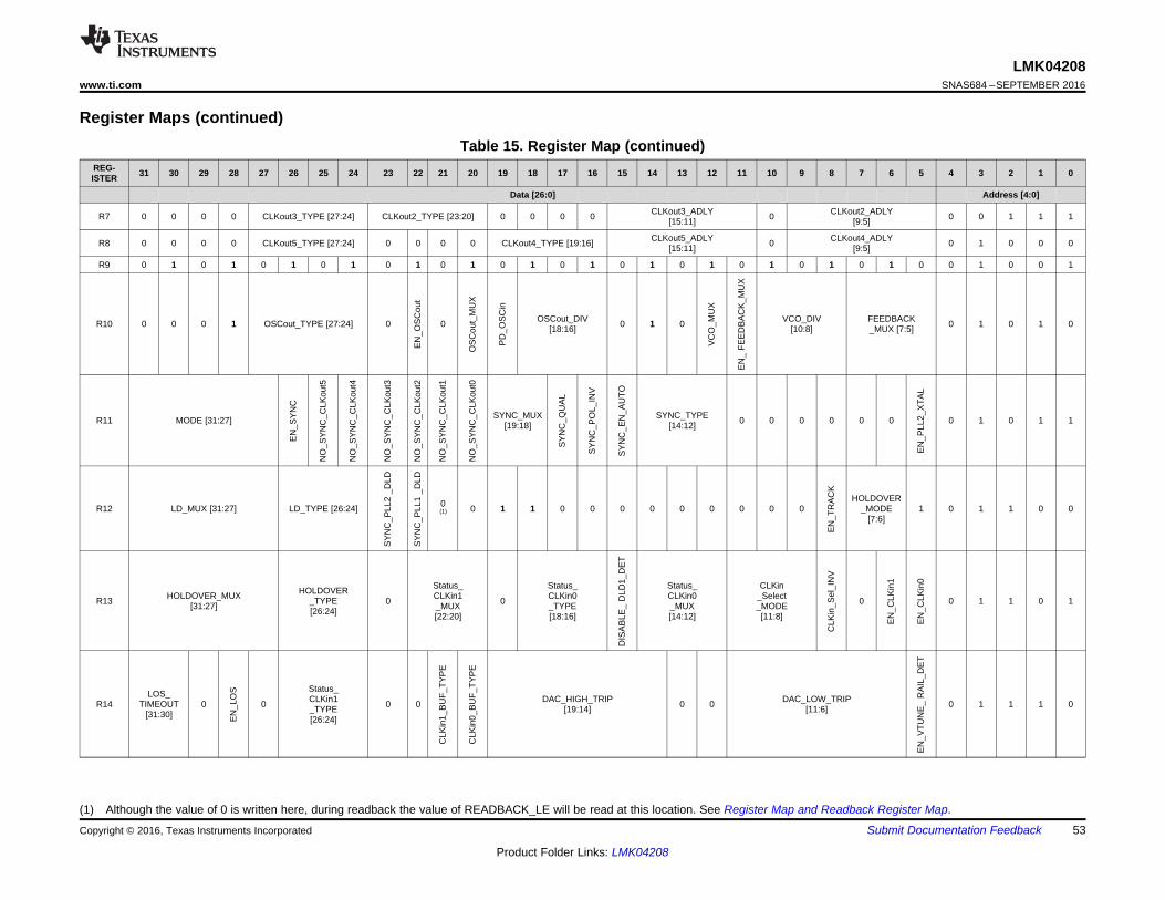
LMK04208www.ti.com SNAS684 –SEPTEMBER 2016
53
Product Folder Links: LMK04208
Submit Documentation FeedbackCopyright © 2016, Texas Instruments Incorporated
Register Maps (continued)Table 15. Register Map (continued)
REG-ISTER 31 30 29 28 27 26 25 24 23 22 21 20 19 18 17 16 15 14 13 12 11 10 9 8 7 6 5 4 3 2 1 0
Data [26:0] Address [4:0]
(1) Although the value of 0 is written here, during readback the value of READBACK_LE will be read at this location. See Register Map and Readback Register Map.
R7 0 0 0 0 CLKout3_TYPE [27:24] CLKout2_TYPE [23:20] 0 0 0 0 CLKout3_ADLY[15:11] 0 CLKout2_ADLY
[9:5] 0 0 1 1 1
R8 0 0 0 0 CLKout5_TYPE [27:24] 0 0 0 0 CLKout4_TYPE [19:16] CLKout5_ADLY[15:11] 0 CLKout4_ADLY
[9:5] 0 1 0 0 0
R9 0 1 0 1 0 1 0 1 0 1 0 1 0 1 0 1 0 1 0 1 0 1 0 1 0 1 0 0 1 0 0 1
R10 0 0 0 1 OSCout_TYPE [27:24] 0
EN
_OS
Cou
t
0
OS
Cou
t_M
UX
PD
_OS
Cin
OSCout_DIV[18:16] 0 1 0
VC
O_M
UX
EN
_FE
ED
BA
CK
_MU
X
VCO_DIV[10:8]
FEEDBACK_MUX [7:5] 0 1 0 1 0
R11 MODE [31:27]
EN
_SY
NC
NO
_SY
NC
_CLK
out5
NO
_SY
NC
_CLK
out4
NO
_SY
NC
_CLK
out3
NO
_SY
NC
_CLK
out2
NO
_SY
NC
_CLK
out1
NO
_SY
NC
_CLK
out0
SYNC_MUX[19:18]
SY
NC
_QU
AL
SY
NC
_PO
L_IN
V
SY
NC
_EN
_AU
TO
SYNC_TYPE[14:12] 0 0 0 0 0 0
EN
_PLL
2_X
TAL
0 1 0 1 1
R12 LD_MUX [31:27] LD_TYPE [26:24]
SY
NC
_PLL
2_D
LD
SY
NC
_PLL
1_D
LD
0(1) 0 1 1 0 0 0 0 0 0 0 0 0
EN
_TR
AC
K
HOLDOVER_MODE
[7:6]1 0 1 1 0 0
R13 HOLDOVER_MUX[31:27]
HOLDOVER_TYPE[26:24]
0
Status_CLKin1_MUX[22:20]
0
Status_CLKin0_TYPE[18:16]
DIS
AB
LE_
DLD
1_D
ET
Status_CLKin0_MUX[14:12]
CLKin_Select_MODE[11:8]
CLK
in_S
el_I
NV
0
EN
_CLK
in1
EN
_CLK
in0
0 1 1 0 1
R14LOS_
TIMEOUT[31:30]
0
EN
_LO
S
0
Status_CLKin1_TYPE[26:24]
0 0
CLK
in1_
BU
F_TY
PE
CLK
in0_
BU
F_TY
PE
DAC_HIGH_TRIP[19:14] 0 0 DAC_LOW_TRIP
[11:6]
EN
_VTU
NE
_R
AIL
_DE
T
0 1 1 1 0
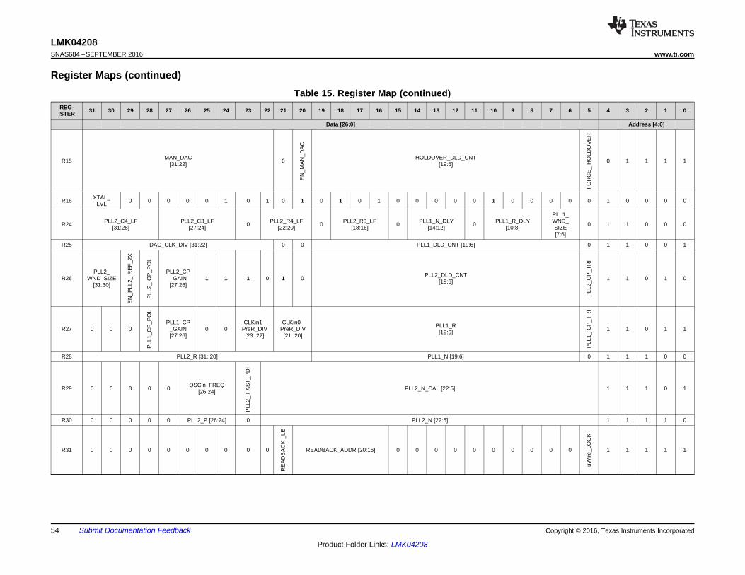
LMK04208SNAS684 –SEPTEMBER 2016 www.ti.com
54
Product Folder Links: LMK04208
Submit Documentation Feedback Copyright © 2016, Texas Instruments Incorporated
Register Maps (continued)Table 15. Register Map (continued)
REG-ISTER 31 30 29 28 27 26 25 24 23 22 21 20 19 18 17 16 15 14 13 12 11 10 9 8 7 6 5 4 3 2 1 0
Data [26:0] Address [4:0]
R15 MAN_DAC[31:22] 0
EN
_MA
N_D
AC
HOLDOVER_DLD_CNT[19:6]
FOR
CE
_H
OLD
OV
ER
0 1 1 1 1
R16 XTAL_LVL 0 0 0 0 0 1 0 1 0 1 0 1 0 1 0 0 0 0 0 1 0 0 0 0 0 1 0 0 0 0
R24 PLL2_C4_LF[31:28]
PLL2_C3_LF[27:24] 0 PLL2_R4_LF
[22:20] 0 PLL2_R3_LF[18:16] 0 PLL1_N_DLY
[14:12] 0 PLL1_R_DLY[10:8]
PLL1_WND_SIZE[7:6]
0 1 1 0 0 0
R25 DAC_CLK_DIV [31:22] 0 0 PLL1_DLD_CNT [19:6] 0 1 1 0 0 1
R26PLL2_
WND_SIZE[31:30]
EN
_PLL
2_R
EF_
2X
PLL
2_C
P_P
OL
PLL2_CP_GAIN[27:26]
1 1 1 0 1 0 PLL2_DLD_CNT[19:6]
PLL
2_C
P_T
RI
1 1 0 1 0
R27 0 0 0
PLL
1_C
P_P
OL
PLL1_CP_GAIN[27:26]
0 0CLKin1_
PreR_DIV[23: 22]
CLKin0_PreR_DIV
[21: 20]
PLL1_R[19:6]
PLL
1_C
P_T
RI
1 1 0 1 1
R28 PLL2_R [31: 20] PLL1_N [19:6] 0 1 1 1 0 0
R29 0 0 0 0 0 OSCin_FREQ[26:24]
PLL
2_FA
ST_
PD
F
PLL2_N_CAL [22:5] 1 1 1 0 1
R30 0 0 0 0 0 PLL2_P [26:24] 0 PLL2_N [22:5] 1 1 1 1 0
R31 0 0 0 0 0 0 0 0 0 0
RE
AD
BA
CK
_LE
READBACK_ADDR [20:16] 0 0 0 0 0 0 0 0 0 0
uWire
_LO
CK
1 1 1 1 1
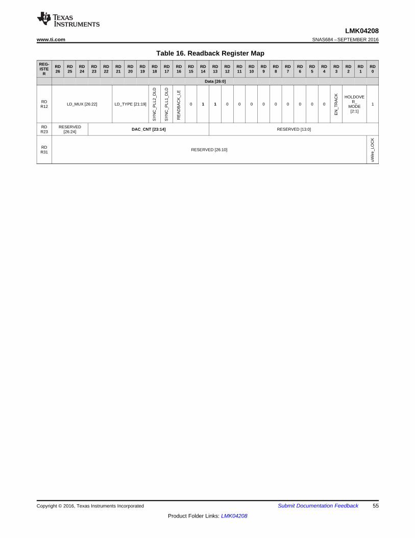
55
LMK04208www.ti.com SNAS684 –SEPTEMBER 2016
Product Folder Links: LMK04208
Submit Documentation FeedbackCopyright © 2016, Texas Instruments Incorporated
Table 16. Readback Register MapREG-ISTE
R
RD26
RD25
RD24
RD23
RD22
RD21
RD20
RD19
RD18
RD17
RD16
RD15
RD14
RD13
RD12
RD11
RD10
RD9
RD8
RD7
RD6
RD5
RD4
RD3
RD2
RD1
RD0
Data [26:0]
RDR12 LD_MUX [26:22] LD_TYPE [21:19]
SY
NC
_PLL
2_D
LD
SY
NC
_PLL
1_D
LD
RE
AD
BA
CK
_LE
0 1 1 0 0 0 0 0 0 0 0 0
EN
_TR
AC
K HOLDOVER_
MODE[2:1]
1
RDR23
RESERVED[26:24] DAC_CNT [23:14] RESERVED [13:0]
RDR31 RESERVED [26:10]
uWire
_LO
CK
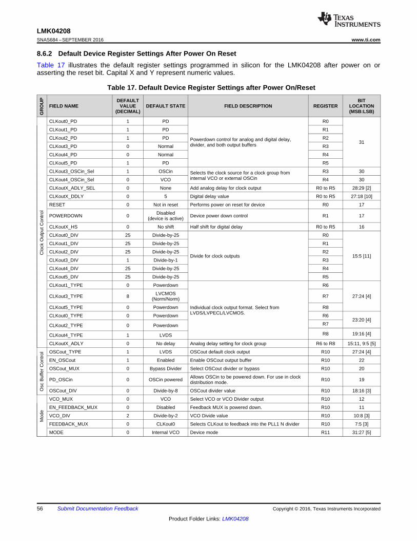
56
LMK04208SNAS684 –SEPTEMBER 2016 www.ti.com
Product Folder Links: LMK04208
Submit Documentation Feedback Copyright © 2016, Texas Instruments Incorporated
8.6.2 Default Device Register Settings After Power On ResetTable 17 illustrates the default register settings programmed in silicon for the LMK04208 after power on orasserting the reset bit. Capital X and Y represent numeric values.
Table 17. Default Device Register Settings after Power On/Reset
GR
OU
P
FIELD NAMEDEFAULT
VALUE(DECIMAL)
DEFAULT STATE FIELD DESCRIPTION REGISTERBIT
LOCATION(MSB:LSB)
Clo
ckO
utpu
tCon
trol
CLKout0_PD 1 PD
Powerdown control for analog and digital delay,divider, and both output buffers
R0
31
CLKout1_PD 1 PD R1
CLKout2_PD 1 PD R2
CLKout3_PD 0 Normal R3
CLKout4_PD 0 Normal R4
CLKout5_PD 1 PD R5
CLKout3_OSCin_Sel 1 OSCin Selects the clock source for a clock group frominternal VCO or external OSCin
R3 30
CLKout4_OSCin_Sel 0 VCO R4 30
CLKoutX_ADLY_SEL 0 None Add analog delay for clock output R0 to R5 28:29 [2]
CLKoutX_DDLY 0 5 Digital delay value R0 to R5 27:18 [10]
RESET 0 Not in reset Performs power on reset for device R0 17
POWERDOWN 0 Disabled(device is active) Device power down control R1 17
CLKoutX_HS 0 No shift Half shift for digital delay R0 to R5 16
CLKout0_DIV 25 Divide-by-25
Divide for clock outputs
R0
15:5 [11]
CLKout1_DIV 25 Divide-by-25 R1
CLKout2_DIV 25 Divide-by-25 R2
CLKout3_DIV 1 Divide-by-1 R3
CLKout4_DIV 25 Divide-by-25 R4
CLKout5_DIV 25 Divide-by-25 R5
CLKout1_TYPE 0 Powerdown
Individual clock output format. Select fromLVDS/LVPECL/LVCMOS.
R6
27:24 [4]CLKout3_TYPE 8 LVCMOS(Norm/Norm) R7
CLKout5_TYPE 0 Powerdown R8
CLKout0_TYPE 0 Powerdown R623:20 [4]
CLKout2_TYPE 0 Powerdown R7
R8 19:16 [4]CLKout4_TYPE 1 LVDS
CLKoutX_ADLY 0 No delay Analog delay setting for clock group R6 to R8 15:11, 9:5 [5]
Osc
Buf
ferC
ontro
l OSCout_TYPE 1 LVDS OSCout default clock output R10 27:24 [4]
EN_OSCout 1 Enabled Enable OSCout output buffer R10 22
OSCout_MUX 0 Bypass Divider Select OSCout divider or bypass R10 20
PD_OSCin 0 OSCin powered Allows OSCin to be powered down. For use in clockdistribution mode. R10 19
OSCout_DIV 0 Divide-by-8 OSCout divider value R10 18:16 [3]
Mod
e
VCO_MUX 0 VCO Select VCO or VCO Divider output R10 12
EN_FEEDBACK_MUX 0 Disabled Feedback MUX is powered down. R10 11
VCO_DIV 2 Divide-by-2 VCO Divide value R10 10:8 [3]
FEEDBACK_MUX 0 CLKout0 Selects CLKout to feedback into the PLL1 N divider R10 7:5 [3]
MODE 0 Internal VCO Device mode R11 31:27 [5]
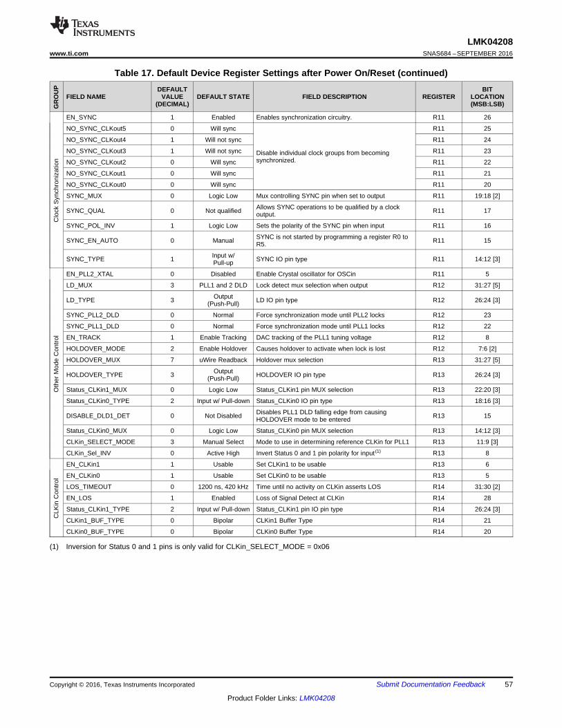
57
LMK04208www.ti.com SNAS684 –SEPTEMBER 2016
Product Folder Links: LMK04208
Submit Documentation FeedbackCopyright © 2016, Texas Instruments Incorporated
Table 17. Default Device Register Settings after Power On/Reset (continued)
GR
OU
P
FIELD NAMEDEFAULT
VALUE(DECIMAL)
DEFAULT STATE FIELD DESCRIPTION REGISTERBIT
LOCATION(MSB:LSB)
(1) Inversion for Status 0 and 1 pins is only valid for CLKin_SELECT_MODE = 0x06
Clo
ckS
ynch
roni
zatio
n
EN_SYNC 1 Enabled Enables synchronization circuitry. R11 26
NO_SYNC_CLKout5 0 Will sync
Disable individual clock groups from becomingsynchronized.
R11 25
NO_SYNC_CLKout4 1 Will not sync R11 24
NO_SYNC_CLKout3 1 Will not sync R11 23
NO_SYNC_CLKout2 0 Will sync R11 22
NO_SYNC_CLKout1 0 Will sync R11 21
NO_SYNC_CLKout0 0 Will sync R11 20
SYNC_MUX 0 Logic Low Mux controlling SYNC pin when set to output R11 19:18 [2]
SYNC_QUAL 0 Not qualified Allows SYNC operations to be qualified by a clockoutput. R11 17
SYNC_POL_INV 1 Logic Low Sets the polarity of the SYNC pin when input R11 16
SYNC_EN_AUTO 0 Manual SYNC is not started by programming a register R0 toR5. R11 15
SYNC_TYPE 1 Input w/Pull-up SYNC IO pin type R11 14:12 [3]
Oth
erM
ode
Con
trol
EN_PLL2_XTAL 0 Disabled Enable Crystal oscillator for OSCin R11 5
LD_MUX 3 PLL1 and 2 DLD Lock detect mux selection when output R12 31:27 [5]
LD_TYPE 3 Output(Push-Pull) LD IO pin type R12 26:24 [3]
SYNC_PLL2_DLD 0 Normal Force synchronization mode until PLL2 locks R12 23
SYNC_PLL1_DLD 0 Normal Force synchronization mode until PLL1 locks R12 22
EN_TRACK 1 Enable Tracking DAC tracking of the PLL1 tuning voltage R12 8
HOLDOVER_MODE 2 Enable Holdover Causes holdover to activate when lock is lost R12 7:6 [2]
HOLDOVER_MUX 7 uWire Readback Holdover mux selection R13 31:27 [5]
HOLDOVER_TYPE 3 Output(Push-Pull) HOLDOVER IO pin type R13 26:24 [3]
Status_CLKin1_MUX 0 Logic Low Status_CLKin1 pin MUX selection R13 22:20 [3]
Status_CLKin0_TYPE 2 Input w/ Pull-down Status_CLKin0 IO pin type R13 18:16 [3]
DISABLE_DLD1_DET 0 Not Disabled Disables PLL1 DLD falling edge from causingHOLDOVER mode to be entered R13 15
Status_CLKin0_MUX 0 Logic Low Status_CLKin0 pin MUX selection R13 14:12 [3]
CLKin_SELECT_MODE 3 Manual Select Mode to use in determining reference CLKin for PLL1 R13 11:9 [3]
CLKin_Sel_INV 0 Active High Invert Status 0 and 1 pin polarity for input (1) R13 8
CLK
inC
ontro
l
EN_CLKin1 1 Usable Set CLKin1 to be usable R13 6
EN_CLKin0 1 Usable Set CLKin0 to be usable R13 5
LOS_TIMEOUT 0 1200 ns, 420 kHz Time until no activity on CLKin asserts LOS R14 31:30 [2]
EN_LOS 1 Enabled Loss of Signal Detect at CLKin R14 28
Status_CLKin1_TYPE 2 Input w/ Pull-down Status_CLKin1 pin IO pin type R14 26:24 [3]
CLKin1_BUF_TYPE 0 Bipolar CLKin1 Buffer Type R14 21
CLKin0_BUF_TYPE 0 Bipolar CLKin0 Buffer Type R14 20
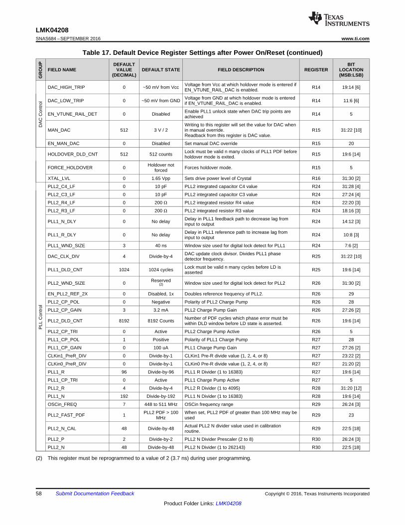
58
LMK04208SNAS684 –SEPTEMBER 2016 www.ti.com
Product Folder Links: LMK04208
Submit Documentation Feedback Copyright © 2016, Texas Instruments Incorporated
Table 17. Default Device Register Settings after Power On/Reset (continued)
GR
OU
P
FIELD NAMEDEFAULT
VALUE(DECIMAL)
DEFAULT STATE FIELD DESCRIPTION REGISTERBIT
LOCATION(MSB:LSB)
(2) This register must be reprogrammed to a value of 2 (3.7 ns) during user programming.
DA
CC
ontro
l
DAC_HIGH_TRIP 0 ~50 mV from Vcc Voltage from Vcc at which holdover mode is entered ifEN_VTUNE_RAIL_DAC is enabled. R14 19:14 [6]
DAC_LOW_TRIP 0 ~50 mV from GND Voltage from GND at which holdover mode is enteredif EN_VTUNE_RAIL_DAC is enabled. R14 11:6 [6]
EN_VTUNE_RAIL_DET 0 Disabled Enable PLL1 unlock state when DAC trip points areachieved R14 5
MAN_DAC 512 3 V / 2Writing to this register will set the value for DAC whenin manual override.Readback from this register is DAC value.
R15 31:22 [10]
EN_MAN_DAC 0 Disabled Set manual DAC override R15 20
HOLDOVER_DLD_CNT 512 512 counts Lock must be valid n many clocks of PLL1 PDF beforeholdover mode is exited. R15 19:6 [14]
FORCE_HOLDOVER 0 Holdover notforced Forces holdover mode. R15 5
XTAL_LVL 0 1.65 Vpp Sets drive power level of Crystal R16 31:30 [2]
PLL
Con
trol
PLL2_C4_LF 0 10 pF PLL2 integrated capacitor C4 value R24 31:28 [4]
PLL2_C3_LF 0 10 pF PLL2 integrated capacitor C3 value R24 27:24 [4]
PLL2_R4_LF 0 200 Ω PLL2 integrated resistor R4 value R24 22:20 [3]
PLL2_R3_LF 0 200 Ω PLL2 integrated resistor R3 value R24 18:16 [3]
PLL1_N_DLY 0 No delay Delay in PLL1 feedback path to decrease lag frominput to output R24 14:12 [3]
PLL1_R_DLY 0 No delay Delay in PLL1 reference path to increase lag frominput to output R24 10:8 [3]
PLL1_WND_SIZE 3 40 ns Window size used for digital lock detect for PLL1 R24 7:6 [2]
DAC_CLK_DIV 4 Divide-by-4 DAC update clock divisor. Divides PLL1 phasedetector frequency. R25 31:22 [10]
PLL1_DLD_CNT 1024 1024 cycles Lock must be valid n many cycles before LD isasserted R25 19:6 [14]
PLL2_WND_SIZE 0 Reserved(2) Window size used for digital lock detect for PLL2 R26 31:30 [2]
EN_PLL2_REF_2X 0 Disabled, 1x Doubles reference frequency of PLL2. R26 29
PLL2_CP_POL 0 Negative Polarity of PLL2 Charge Pump R26 28
PLL2_CP_GAIN 3 3.2 mA PLL2 Charge Pump Gain R26 27:26 [2]
PLL2_DLD_CNT 8192 8192 Counts Number of PDF cycles which phase error must bewithin DLD window before LD state is asserted. R26 19:6 [14]
PLL2_CP_TRI 0 Active PLL2 Charge Pump Active R26 5
PLL1_CP_POL 1 Positive Polarity of PLL1 Charge Pump R27 28
PLL1_CP_GAIN 0 100 uA PLL1 Charge Pump Gain R27 27:26 [2]
CLKin1_PreR_DIV 0 Divide-by-1 CLKin1 Pre-R divide value (1, 2, 4, or 8) R27 23:22 [2]
CLKin0_PreR_DIV 0 Divide-by-1 CLKin0 Pre-R divide value (1, 2, 4, or 8) R27 21:20 [2]
PLL1_R 96 Divide-by-96 PLL1 R Divider (1 to 16383) R27 19:6 [14]
PLL1_CP_TRI 0 Active PLL1 Charge Pump Active R27 5
PLL2_R 4 Divide-by-4 PLL2 R Divider (1 to 4095) R28 31:20 [12]
PLL1_N 192 Divide-by-192 PLL1 N Divider (1 to 16383) R28 19:6 [14]
OSCin_FREQ 7 448 to 511 MHz OSCin frequency range R29 26:24 [3]
PLL2_FAST_PDF 1 PLL2 PDF > 100MHz
When set, PLL2 PDF of greater than 100 MHz may beused R29 23
PLL2_N_CAL 48 Divide-by-48 Actual PLL2 N divider value used in calibrationroutine. R29 22:5 [18]
PLL2_P 2 Divide-by-2 PLL2 N Divider Prescaler (2 to 8) R30 26:24 [3]
PLL2_N 48 Divide-by-48 PLL2 N Divider (1 to 262143) R30 22:5 [18]
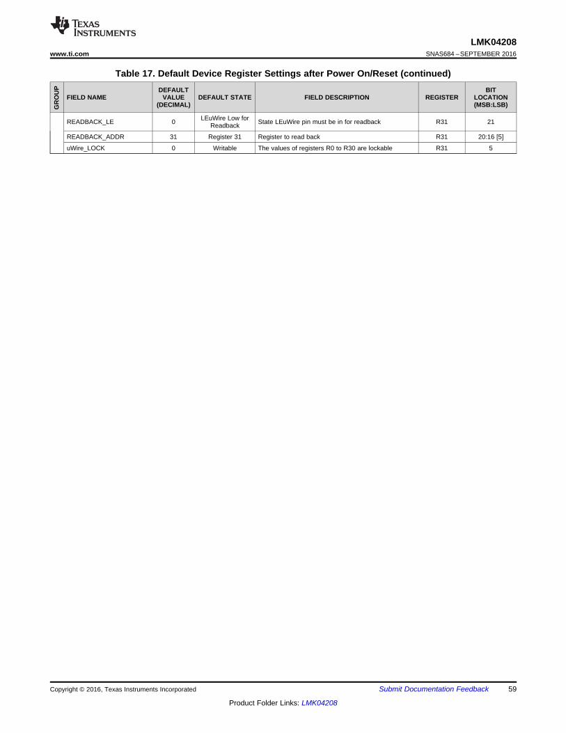
59
LMK04208www.ti.com SNAS684 –SEPTEMBER 2016
Product Folder Links: LMK04208
Submit Documentation FeedbackCopyright © 2016, Texas Instruments Incorporated
Table 17. Default Device Register Settings after Power On/Reset (continued)
GR
OU
P
FIELD NAMEDEFAULT
VALUE(DECIMAL)
DEFAULT STATE FIELD DESCRIPTION REGISTERBIT
LOCATION(MSB:LSB)
READBACK_LE 0 LEuWire Low forReadback State LEuWire pin must be in for readback R31 21
READBACK_ADDR 31 Register 31 Register to read back R31 20:16 [5]
uWire_LOCK 0 Writable The values of registers R0 to R30 are lockable R31 5
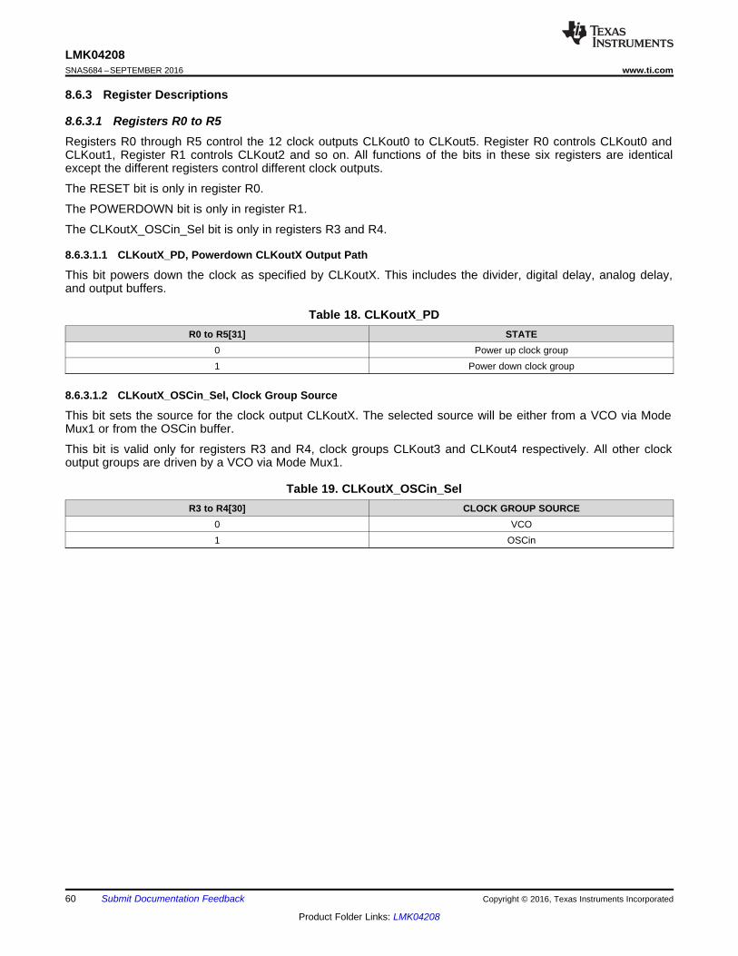
60
LMK04208SNAS684 –SEPTEMBER 2016 www.ti.com
Product Folder Links: LMK04208
Submit Documentation Feedback Copyright © 2016, Texas Instruments Incorporated
8.6.3 Register Descriptions
8.6.3.1 Registers R0 to R5Registers R0 through R5 control the 12 clock outputs CLKout0 to CLKout5. Register R0 controls CLKout0 andCLKout1, Register R1 controls CLKout2 and so on. All functions of the bits in these six registers are identicalexcept the different registers control different clock outputs.
The RESET bit is only in register R0.
The POWERDOWN bit is only in register R1.
The CLKoutX_OSCin_Sel bit is only in registers R3 and R4.
8.6.3.1.1 CLKoutX_PD, Powerdown CLKoutX Output Path
This bit powers down the clock as specified by CLKoutX. This includes the divider, digital delay, analog delay,and output buffers.
Table 18. CLKoutX_PDR0 to R5[31] STATE
0 Power up clock group1 Power down clock group
8.6.3.1.2 CLKoutX_OSCin_Sel, Clock Group Source
This bit sets the source for the clock output CLKoutX. The selected source will be either from a VCO via ModeMux1 or from the OSCin buffer.
This bit is valid only for registers R3 and R4, clock groups CLKout3 and CLKout4 respectively. All other clockoutput groups are driven by a VCO via Mode Mux1.
Table 19. CLKoutX_OSCin_SelR3 to R4[30] CLOCK GROUP SOURCE
0 VCO1 OSCin
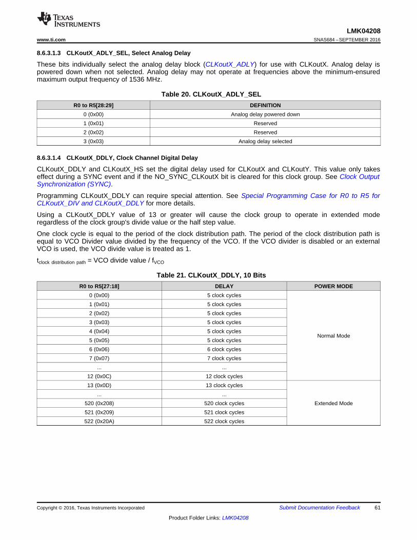
61
LMK04208www.ti.com SNAS684 –SEPTEMBER 2016
Product Folder Links: LMK04208
Submit Documentation FeedbackCopyright © 2016, Texas Instruments Incorporated
8.6.3.1.3 CLKoutX_ADLY_SEL, Select Analog Delay
These bits individually select the analog delay block (CLKoutX_ADLY) for use with CLKoutX. Analog delay ispowered down when not selected. Analog delay may not operate at frequencies above the minimum-ensuredmaximum output frequency of 1536 MHz.
Table 20. CLKoutX_ADLY_SELR0 to R5[28:29] DEFINITION
0 (0x00) Analog delay powered down1 (0x01) Reserved2 (0x02) Reserved3 (0x03) Analog delay selected
8.6.3.1.4 CLKoutX_DDLY, Clock Channel Digital Delay
CLKoutX_DDLY and CLKoutX_HS set the digital delay used for CLKoutX and CLKoutY. This value only takeseffect during a SYNC event and if the NO_SYNC_CLKoutX bit is cleared for this clock group. See Clock OutputSynchronization (SYNC).
Programming CLKoutX_DDLY can require special attention. See Special Programming Case for R0 to R5 forCLKoutX_DIV and CLKoutX_DDLY for more details.
Using a CLKoutX_DDLY value of 13 or greater will cause the clock group to operate in extended moderegardless of the clock group's divide value or the half step value.
One clock cycle is equal to the period of the clock distribution path. The period of the clock distribution path isequal to VCO Divider value divided by the frequency of the VCO. If the VCO divider is disabled or an externalVCO is used, the VCO divide value is treated as 1.
tclock distribution path = VCO divide value / fVCO
Table 21. CLKoutX_DDLY, 10 BitsR0 to R5[27:18] DELAY POWER MODE
0 (0x00) 5 clock cycles
Normal Mode
1 (0x01) 5 clock cycles2 (0x02) 5 clock cycles3 (0x03) 5 clock cycles4 (0x04) 5 clock cycles5 (0x05) 5 clock cycles6 (0x06) 6 clock cycles7 (0x07) 7 clock cycles
... ...12 (0x0C) 12 clock cycles13 (0x0D) 13 clock cycles
Extended Mode... ...
520 (0x208) 520 clock cycles521 (0x209) 521 clock cycles522 (0x20A) 522 clock cycles
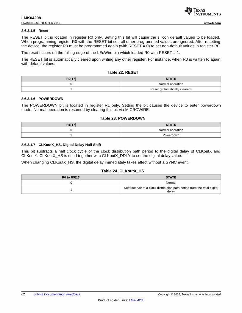
62
LMK04208SNAS684 –SEPTEMBER 2016 www.ti.com
Product Folder Links: LMK04208
Submit Documentation Feedback Copyright © 2016, Texas Instruments Incorporated
8.6.3.1.5 Reset
The RESET bit is located in register R0 only. Setting this bit will cause the silicon default values to be loaded.When programming register R0 with the RESET bit set, all other programmed values are ignored. After resettingthe device, the register R0 must be programmed again (with RESET = 0) to set non-default values in register R0.
The reset occurs on the falling edge of the LEuWire pin which loaded R0 with RESET = 1.
The RESET bit is automatically cleared upon writing any other register. For instance, when R0 is written to againwith default values.
Table 22. RESETR0[17] STATE
0 Normal operation1 Reset (automatically cleared)
8.6.3.1.6 POWERDOWN
The POWERDOWN bit is located in register R1 only. Setting the bit causes the device to enter powerdownmode. Normal operation is resumed by clearing this bit via MICROWIRE.
Table 23. POWERDOWNR1[17] STATE
0 Normal operation1 Powerdown
8.6.3.1.7 CLKoutX_HS, Digital Delay Half Shift
This bit subtracts a half clock cycle of the clock distribution path period to the digital delay of CLKoutX andCLKoutY. CLKoutX_HS is used together with CLKoutX_DDLY to set the digital delay value.
When changing CLKoutX_HS, the digital delay immediately takes effect without a SYNC event.
Table 24. CLKoutX_HSR0 to R5[16] STATE
0 Normal
1 Subtract half of a clock distribution path period from the total digitaldelay
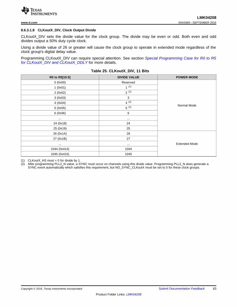
63
LMK04208www.ti.com SNAS684 –SEPTEMBER 2016
Product Folder Links: LMK04208
Submit Documentation FeedbackCopyright © 2016, Texas Instruments Incorporated
(1) CLKoutX_HS must = 0 for divide by 1.(2) After programming PLL2_N value, a SYNC must occur on channels using this divide value. Programming PLL2_N does generate a
SYNC event automatically which satisfies this requirement, but NO_SYNC_CLKoutX must be set to 0 for these clock groups.
8.6.3.1.8 CLKoutX_DIV, Clock Output Divide
CLKoutX_DIV sets the divide value for the clock group. The divide may be even or odd. Both even and odddivides output a 50% duty cycle clock.
Using a divide value of 26 or greater will cause the clock group to operate in extended mode regardless of theclock group's digital delay value.
Programming CLKoutX_DIV can require special attention. See section Special Programming Case for R0 to R5for CLKoutX_DIV and CLKoutX_DDLY for more details.
Table 25. CLKoutX_DIV, 11 BitsR0 to R5[15:5] DIVIDE VALUE POWER MODE
0 (0x00) Reserved
Normal Mode
1 (0x01) 1 (1)
2 (0x02) 2 (2)
3 (0x03) 34 (0x04) 4 (2)
5 (0x05) 5 (2)
6 (0x06) 6... ...
24 (0x18) 2425 (0x19) 2526 (0x1A) 26
Extended Mode27 (0x1B) 27
... ...1044 (0x414) 10441045 (0x415) 1045
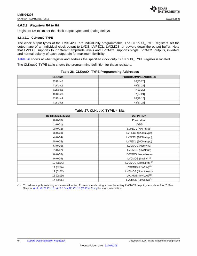
64
LMK04208SNAS684 –SEPTEMBER 2016 www.ti.com
Product Folder Links: LMK04208
Submit Documentation Feedback Copyright © 2016, Texas Instruments Incorporated
8.6.3.2 Registers R6 to R8Registers R6 to R8 set the clock output types and analog delays.
8.6.3.2.1 CLKoutX_TYPE
The clock output types of the LMK04208 are individually programmable. The CLKoutX_TYPE registers set theoutput type of an individual clock output to LVDS, LVPECL, LVCMOS, or powers down the output buffer. Notethat LVPECL supports four different amplitude levels and LVCMOS supports single LVCMOS outputs, inverted,and normal polarity of each output pin for maximum flexibility.
Table 26 shows at what register and address the specified clock output CLKoutX_TYPE register is located.
The CLKoutX_TYPE table shows the programming definition for these registers.
Table 26. CLKoutX_TYPE Programming AddressesCLKoutX PROGRAMMING ADDRESSCLKout0 R6[23:20]CLKout1 R6[27:24]CLKout2 R7[23:20]CLKout3 R7[27:24]CLKout4 R8[19:16]CLKout5 R8[27:24]
(1) To reduce supply switching and crosstalk noise, TI recommends using a complementary LVCMOS output type such as 6 or 7. SeeSection Vcc2, Vcc3, Vcc10, Vcc11, Vcc12, Vcc13 (CLKout Vccs) for more information
Table 27. CLKoutX_TYPE, 4 BitsR6-R8[27:24, 23:20] DEFINITION
0 (0x00) Power down1 (0x01) LVDS2 (0x02) LVPECL (700 mVpp)3 (0x03) LVPECL (1200 mVpp)4 (0x04) LVPECL (1600 mVpp)5 (0x05) LVPECL (2000 mVpp)6 (0x06) LVCMOS (Norm/Inv)7 (0x07) LVCMOS (Inv/Norm)8 (0x08) LVCMOS (Norm/Norm)9 (0x09) LVCMOS (Inv/Inv) (1)
10 (0x0A) LVCMOS (Low/Norm) (1)
11 (0x0A) LVCMOS (Low/Inv) (1)
12 (0x0C) LVCMOS (Norm/Low) (1)
13 (0x0D) LVCMOS (Inv/Low) (1)
14 (0x0E) LVCMOS (Low/Low) (1)
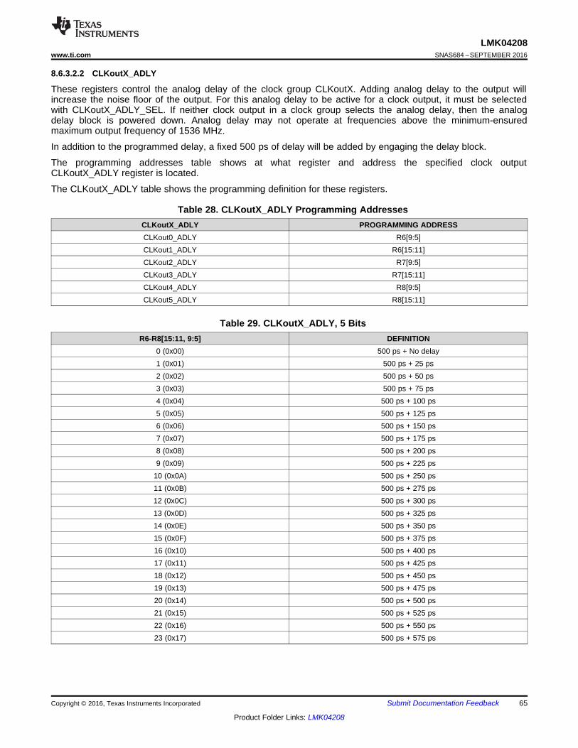
65
LMK04208www.ti.com SNAS684 –SEPTEMBER 2016
Product Folder Links: LMK04208
Submit Documentation FeedbackCopyright © 2016, Texas Instruments Incorporated
8.6.3.2.2 CLKoutX_ADLY
These registers control the analog delay of the clock group CLKoutX. Adding analog delay to the output willincrease the noise floor of the output. For this analog delay to be active for a clock output, it must be selectedwith CLKoutX_ADLY_SEL. If neither clock output in a clock group selects the analog delay, then the analogdelay block is powered down. Analog delay may not operate at frequencies above the minimum-ensuredmaximum output frequency of 1536 MHz.
In addition to the programmed delay, a fixed 500 ps of delay will be added by engaging the delay block.
The programming addresses table shows at what register and address the specified clock outputCLKoutX_ADLY register is located.
The CLKoutX_ADLY table shows the programming definition for these registers.
Table 28. CLKoutX_ADLY Programming AddressesCLKoutX_ADLY PROGRAMMING ADDRESSCLKout0_ADLY R6[9:5]CLKout1_ADLY R6[15:11]CLKout2_ADLY R7[9:5]CLKout3_ADLY R7[15:11]CLKout4_ADLY R8[9:5]CLKout5_ADLY R8[15:11]
Table 29. CLKoutX_ADLY, 5 BitsR6-R8[15:11, 9:5] DEFINITION
0 (0x00) 500 ps + No delay1 (0x01) 500 ps + 25 ps2 (0x02) 500 ps + 50 ps3 (0x03) 500 ps + 75 ps4 (0x04) 500 ps + 100 ps5 (0x05) 500 ps + 125 ps6 (0x06) 500 ps + 150 ps7 (0x07) 500 ps + 175 ps8 (0x08) 500 ps + 200 ps9 (0x09) 500 ps + 225 ps
10 (0x0A) 500 ps + 250 ps11 (0x0B) 500 ps + 275 ps12 (0x0C) 500 ps + 300 ps13 (0x0D) 500 ps + 325 ps14 (0x0E) 500 ps + 350 ps15 (0x0F) 500 ps + 375 ps16 (0x10) 500 ps + 400 ps17 (0x11) 500 ps + 425 ps18 (0x12) 500 ps + 450 ps19 (0x13) 500 ps + 475 ps20 (0x14) 500 ps + 500 ps21 (0x15) 500 ps + 525 ps22 (0x16) 500 ps + 550 ps23 (0x17) 500 ps + 575 ps
66
LMK04208SNAS684 –SEPTEMBER 2016 www.ti.com
Product Folder Links: LMK04208
Submit Documentation Feedback Copyright © 2016, Texas Instruments Incorporated
(1) To reduce supply switching and crosstalk noise, TI recommends using a complementary LVCMOS output type such as 6 or 7. SeeVcc2, Vcc3, Vcc10, Vcc11, Vcc12, Vcc13 (CLKout Vccs) for more information"
8.6.3.3 Register R10
8.6.3.3.1 OSCout_TYPE
The OSCout clock output has a programmable output type. The OSCout_TYPE register sets the output type toLVDS, LVPECL, LVCMOS, or powers down the output buffer. Note that LVPECL supports four differentamplitude levels and LVCMOS supports dual and single LVCMOS outputs with inverted, and normal polarity ofeach output pin for maximum flexibility.
To turn on the output, the OSCout_TYPE must be set to a non-power down setting and enabled withEN_OSCout, OSCout Output Enable.
Table 30. OSCout_TYPE, 4 BitsR10[27:24] DEFINITION
0 (0x00) Powerdown1 (0x01) LVDS2 (0x02) LVPECL (700 mVpp)3 (0x03) LVPECL (1200 mVpp)4 (0x04) LVPECL (1600 mVpp)5 (0x05) LVPECL (2000 mVpp)6 (0x06) LVCMOS (Norm/Inv)7 (0x07) LVCMOS (Inv/Norm)8 (0x08) LVCMOS (Norm/Norm) (1)
9 (0x09) LVCMOS (Inv/Inv) (1)
10 (0x0A) LVCMOS (Low/Norm) (1)
11 (0x0B) LVCMOS (Low/Inv) (1)
12 (0x0C) LVCMOS (Norm/Low) (1)
13 (0x0D) LVCMOS (Inv/Low) (1)
14 (0x0E) LVCMOS (Low/Low) (1)
67
LMK04208www.ti.com SNAS684 –SEPTEMBER 2016
Product Folder Links: LMK04208
Submit Documentation FeedbackCopyright © 2016, Texas Instruments Incorporated
8.6.3.3.2 EN_OSCout, OSCout Output Enable
EN_OSCout is used to enable an oscillator buffered output.
Table 31. EN_OSCoutR10[22] OUTPUT STATE
0 OSCout Disabled1 OSCout Enabled
Note: In addition to enabling the output with EN_OSCout. The OSCout_TYPE must be programmed to a non-power down value for the output buffer to power up.
8.6.3.3.3 OSCout_MUX, Clock Output Mux
Sets OSCout buffer to output a divided or bypassed OSCin signal. The divisor is set by OSCout_DIV, OscillatorOutput Divide.
Table 32. OSCout_MUXR10[20] MUX OUTPUT
0 Bypass divider1 Divided
8.6.3.3.4 PD_OSCin, OSCin Powerdown Control
Except in clock distribution mode, the OSCin buffer must always be powered up.
In clock distribution mode, the OSCin buffer must be powered down if not used.
Table 33. PD_OSCinR10[19] OSCin BUFFER
0 Normal Operation1 Powerdown
68
LMK04208SNAS684 –SEPTEMBER 2016 www.ti.com
Product Folder Links: LMK04208
Submit Documentation Feedback Copyright © 2016, Texas Instruments Incorporated
8.6.3.3.5 OSCout_DIV, Oscillator Output Divide
The OSCout divider can be programmed from 2 to 8. Divide by 1 is achieved by bypassing the divider withOSCout_MUX, Clock Output Mux.
Note that OSCout_DIV will be in the PLL1 N feedback path if OSCout_MUX selects divided as an output. WhenOSCout_DIV is in the PLL1 N feedback path, the OSCout_DIV divide value must be accounted for whenprogramming PLL1 N.
See PLL Programming for more information on programming PLL1 to lock.
Table 34. OSCout_DIV, 3 BitsR10[18:16] DIVIDE
0 (0x00) 81 (0x01) 22 (0x02) 23 (0x03) 34 (0x04) 45 (0x05) 56 (0x06) 67 (0x07) 7
8.6.3.3.6 VCO_MUX
When the internal VCO is used, the VCO divider can be selected to divide the VCO output frequency to reducethe frequency on the clock distribution path. TI recommends using the VCO directly unless:• Very low output frequencies are required.• If using the VCO divider results in three or more clock output divider/delays changing from extended to
normal power mode, a small power savings may be achieved by using the VCO divider.
A consequence of using the VCO divider is a small degradation in phase noise.
Table 35. VCO_MUXR10[12] DEFINITION
0 VCO selected1 VCO divider selected
8.6.3.3.7 EN_FEEDBACK_MUX
When using 0-delay or dynamic digital delay (SYNC_QUAL = 1), EN_FEEDBACK_MUX must be set to 1 topower up the feedback mux.
Table 36. EN_FEEDBACK_MUXR10[11] DEFINITION
0 Feedback mux powered down1 Feedback mux enabled
69
LMK04208www.ti.com SNAS684 –SEPTEMBER 2016
Product Folder Links: LMK04208
Submit Documentation FeedbackCopyright © 2016, Texas Instruments Incorporated
8.6.3.3.8 VCO_DIV, VCO Divider
Divide value of the VCO Divider.
See PLL Programming for more information on programming PLL2 to lock.
Table 37. VCO_DIV, 3 BitsR10[10:8] DIVIDE0 (0x00) 81 (0x01) 22 (0x02) 23 (0x03) 34 (0x04) 45 (0x05) 56 (0x06) 67 (0x07) 7
8.6.3.3.9 FEEDBACK_MUX
When in 0-delay mode, the feedback mux selects the clock output to be fed back into the PLL1 N Divider.
Table 38. FEEDBACK_MUX, 3 BitsR10[7:5] MUX OUTPUT0 (0x00) CLKout01 (0x01) CLKout12 (0x02) CLKout23 (0x03) CLKout34 (0x04) CLKout45 (0x05) CLKout56 (0x06) FBCLKin/FBCLKin*
70
LMK04208SNAS684 –SEPTEMBER 2016 www.ti.com
Product Folder Links: LMK04208
Submit Documentation Feedback Copyright © 2016, Texas Instruments Incorporated
8.6.3.4 Register R11
8.6.3.4.1 MODE: Device Mode
MODE determines how the LMK04208 operates from a high level. Different blocks of the device can be poweredup and down for specific application requirements from a dual loop architecture to clock distribution.
The LMK04208 can operate in:• Dual PLL mode with the internal VCO or an external VCO.• Single PLL mode uses PLL2 and powers down PLL1. OSCin is used for PLL reference input.• Clock Distribution mode allows use of CLKin1 to distribute to clock outputs CLKout0 through CLKout5, and
OSCin to distribute to OSCout, and optionally CLKout3 and CLKout4.
For the PLL modes, deterministic phase delay with respect to the input can be achieved with the 0-delay mode.
For the PLL modes it is also possible to use an external VCO.
Table 39. MODE, 5 BitsR11[31:27] VALUE
0 (0x00) Dual PLL, Internal VCO1 (0x01) Reserved
2 (0x02) Dual PLL, Internal VCO,0-Delay
3 (0x03) Dual PLL, External VCO (Fin)4 (0x04) Reserved5 (0x05) Dual PLL, External VCO (Fin), 0-Delay6 (0x06) PLL2, Internal VCO7 (0x07) Reserved
8 (0x08) PLL2, Internal VCO,0–Delay
9 (0x09) Reserved10 (0x0A) Reserved11 (0x0B) PLL2, External VCO (Fin)12 (0x0C) Reserved13 (0x0D) Reserved14 (0x0E) Reserved15 (0x0F) Reserved16 (0x10) Clock Distribution
71
LMK04208www.ti.com SNAS684 –SEPTEMBER 2016
Product Folder Links: LMK04208
Submit Documentation FeedbackCopyright © 2016, Texas Instruments Incorporated
8.6.3.4.2 EN_SYNC, Enable Synchronization
The EN_SYNC bit (default on) must be enabled for synchronization to work. Synchronization is required fordynamic digital delay.
The synchronization enable may be turned off once the clocks are operating to save current. If EN_SYNC is setafter it has been cleared (a transition from 0 to 1), a SYNC is generated that can disrupt the active clock outputs.Setting the NO_SYNC_CLKoutX bits will prevent this SYNC pulse from affecting the output clocks. Setting theEN_SYNC bit is not a valid method for synchronizing the clock outputs. See the Clock Output Synchronizationsection for more information on synchronization.
Table 40. EN_SYNCR11[26] DEFINITION
0 Synchronization disabled1 Synchronization enabled
8.6.3.4.3 NO_SYNC_CLKoutX
The NO_SYNC_CLKoutX bits prevent individual clock groups from becoming synchronized during a SYNCevent. A reason to prevent individual clock groups from becoming synchronized is that during synchronization,the clock output is in a fixed low state or can have a glitch pulse.
By disabling SYNC on a clock group, it will continue to operate normally during a SYNC event.
Digital delay requires a SYNC operation to take effect. If NO_SYNC_CLKoutX is set before a SYNC event, thedigital delay value will be unused.
Setting the NO_SYNC_CLKoutX bit has no effect on clocks already synchronized together.
Table 41. NO_SYNC_CLKoutX Programming AddressesNO_SYNC_CLKoutX PROGRAMMING ADDRESS
CLKout0 R11:20CLKout1 R11:21CLKout2 R11:22CLKout3 R11:23CLKout4 R11:24CLKout5 R11:25
Table 42. NO_SYNC_CLKoutXR11[25, 24, 23, 22, 21, 20] DEFINITION
0 CLKoutX will synchronize1 CLKoutX will not synchronize
72
LMK04208SNAS684 –SEPTEMBER 2016 www.ti.com
Product Folder Links: LMK04208
Submit Documentation Feedback Copyright © 2016, Texas Instruments Incorporated
8.6.3.4.4 SYNC_MUX
Mux controlling SYNC pin when type is an output.
All the outputs logic is active high when SYNC_TYPE = 3 (Output). All the outputs logic is active low whenSYNC_TYPE = 4 (Output Inverted). For example, when SYNC_MUX = 0 (Logic Low) and SYNC_TYPE = 3(Output) then SYNC outputs a logic low. When SYNC_MUX = 0 (Logic Low) and SYNC_TYPE = 4 (OutputInverted) then SYNC outputs a logic high.
Table 43. SYNC_MUX, 2 BitsR11[19:18] SYNC PIN OUTPUT
0 (0x00) Logic Low1 (0x01) Reserved2 (0x02) Reserved3 (0x03) uWire Readback
8.6.3.4.5 SYNC_QUAL
When SYNC_QUAL is set, clock outputs will be synchronized to an existing clock output selected byFEEDBACK_MUX. By using the NO_SYNC_CLKoutX bits, selected clock outputs will not be interrupted duringthe SYNC event.
Qualifying the SYNC by an output clock means that the pulse which turns the clock outputs off and on will have afixed time relationship to the qualifying output clock.
SYNC_QUAL = 1 requires CLKout2_PD = 0 for proper operation. CLKout2_TYPE may be set to Powerdownmode.
See Clock Output Synchronization (SYNC) for more information.
Table 44. SYNC_QUALR11[17] MODE
0 No qualification
1 Qualification by clock output from feedback mux(Must set CLKout2_PD = 0)
8.6.3.4.6 SYNC_POL_INV
Sets the polarity of the SYNC pin when input. When SYNC is asserted the clock outputs will transition to a lowstate.
See Clock Output Synchronization (SYNC) for more information on SYNC. A SYNC event can be generated bytoggling this bit through the MICROWIRE interface.
Table 45. SYNC_POL_INVR11[16] POLARITY
0 SYNC is active high1 SYNC is active low
73
LMK04208www.ti.com SNAS684 –SEPTEMBER 2016
Product Folder Links: LMK04208
Submit Documentation FeedbackCopyright © 2016, Texas Instruments Incorporated
8.6.3.4.7 SYNC_EN_AUTO
When set, causes a SYNC event to occur when programming register R0 to R5 to adjust digital delay values.
The SYNC event will coincide with the LEuWire pin falling edge.
Refer to Special Programming Case for R0 to R5 for CLKoutX_DIV and CLKoutX_DDLY for more information onpossible special programming considerations when SYNC_EN_AUTO = 1.
Table 46. SYNC_EN_AUTOR11[15] MODE
0 Manual SYNC1 SYNC Internally Generated
8.6.3.4.8 SYNC_TYPE
Sets the IO type of the SYNC pin.
Table 47. SYNC_TYPE, 3 BitsR11[14:12] POLARITY
0 (0x00) Input1 (0x01) Input w/ pull-up resistor2 (0x02) Input w/ pull-down resistor3 (0x03) Output (push-pull)4 (0x04) Output inverted (push-pull)5 (0x05) Output (open source)6 (0x06) Output (open drain)
When in output mode, the SYNC input is forced to 0 regardless of the SYNC_MUX setting. A synchronizationcan then be activated by uWire by programming the SYNC_POL_INV register to active low to assert SYNC.SYNC can then be released by programming SYNC_POL_INV to active high. Using this uWire programmingmethod to create a SYNC event saves the need for an IO pin from another device.
8.6.3.4.9 EN_PLL2_XTAL
If an external crystal is being used to implement a discrete VCXO, the internal feedback amplifier must beenabled with this bit in order to complete the oscillator circuit.
Table 48. EN_PLL2_XTALR11[5] OSCILLATOR AMPLIFIER STATE
0 Disabled1 Enabled
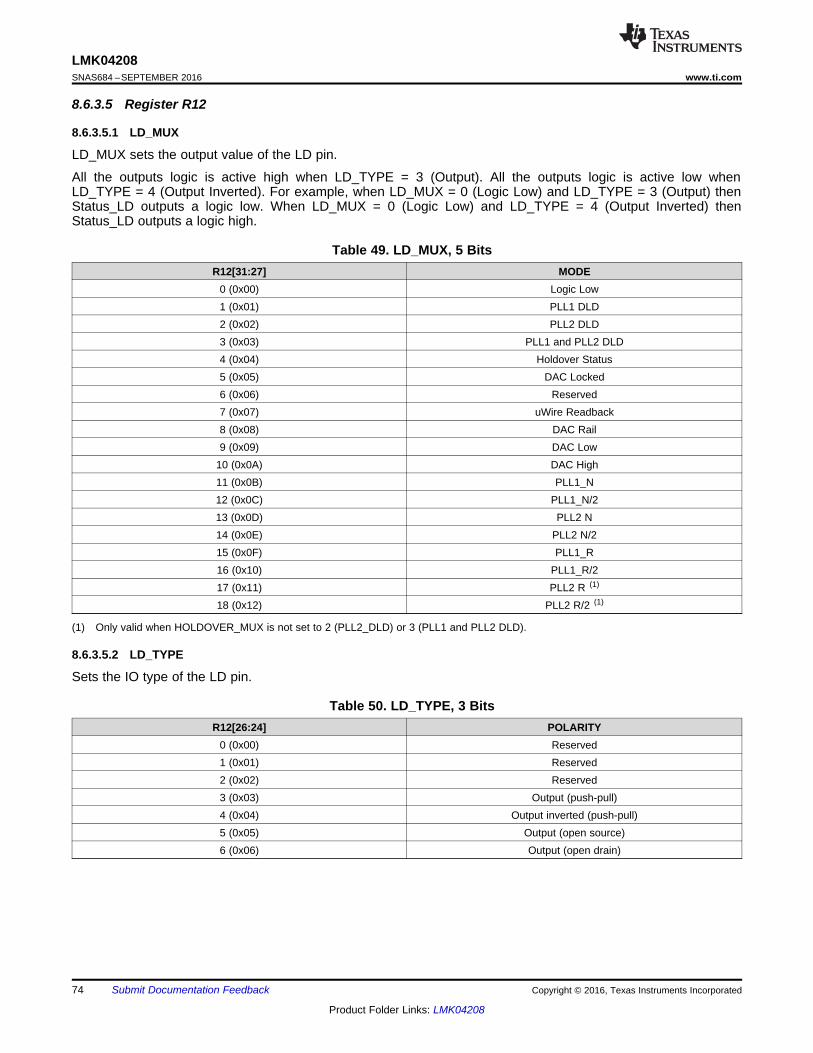
74
LMK04208SNAS684 –SEPTEMBER 2016 www.ti.com
Product Folder Links: LMK04208
Submit Documentation Feedback Copyright © 2016, Texas Instruments Incorporated
(1) Only valid when HOLDOVER_MUX is not set to 2 (PLL2_DLD) or 3 (PLL1 and PLL2 DLD).
8.6.3.5 Register R12
8.6.3.5.1 LD_MUX
LD_MUX sets the output value of the LD pin.
All the outputs logic is active high when LD_TYPE = 3 (Output). All the outputs logic is active low whenLD_TYPE = 4 (Output Inverted). For example, when LD_MUX = 0 (Logic Low) and LD_TYPE = 3 (Output) thenStatus_LD outputs a logic low. When LD_MUX = 0 (Logic Low) and LD_TYPE = 4 (Output Inverted) thenStatus_LD outputs a logic high.
Table 49. LD_MUX, 5 BitsR12[31:27] MODE
0 (0x00) Logic Low1 (0x01) PLL1 DLD2 (0x02) PLL2 DLD3 (0x03) PLL1 and PLL2 DLD4 (0x04) Holdover Status5 (0x05) DAC Locked6 (0x06) Reserved7 (0x07) uWire Readback8 (0x08) DAC Rail9 (0x09) DAC Low
10 (0x0A) DAC High11 (0x0B) PLL1_N12 (0x0C) PLL1_N/213 (0x0D) PLL2 N14 (0x0E) PLL2 N/215 (0x0F) PLL1_R16 (0x10) PLL1_R/217 (0x11) PLL2 R (1)
18 (0x12) PLL2 R/2 (1)
8.6.3.5.2 LD_TYPE
Sets the IO type of the LD pin.
Table 50. LD_TYPE, 3 BitsR12[26:24] POLARITY
0 (0x00) Reserved1 (0x01) Reserved2 (0x02) Reserved3 (0x03) Output (push-pull)4 (0x04) Output inverted (push-pull)5 (0x05) Output (open source)6 (0x06) Output (open drain)
75
LMK04208www.ti.com SNAS684 –SEPTEMBER 2016
Product Folder Links: LMK04208
Submit Documentation FeedbackCopyright © 2016, Texas Instruments Incorporated
8.6.3.5.3 SYNC_PLLX_DLD
By setting SYNC_PLLX_DLD a SYNC mode will be engaged (asserted SYNC) until PLL1 and/or PLL2 locks.
SYNC_QUAL must be 0 to use this functionality.
Table 51. SYNC_PLL2_DLDR12[23] SYNC MODE FORCED
0 No1 Yes
Table 52. SYNC_PLL1_DLDR12[22] SYNC MODE FORCED
0 No1 Yes
8.6.3.5.4 EN_TRACK
Enable the DAC to track the PLL1 tuning voltage. For optional use in in holdover mode.
Tracking can be used to monitor PLL1 voltage by readback of DAC_CNT register in any mode.
Table 53. EN_TRACKR12[8] DAC TRACKING
0 Disabled1 Enabled
8.6.3.5.5 HOLDOVER_MODE
Enable the holdover mode.
Table 54. HOLDOVER_MODE, 2 BitsR12[7:6] HOLDOVER MODE
0 Reserved1 Disabled2 Enabled3 Reserved
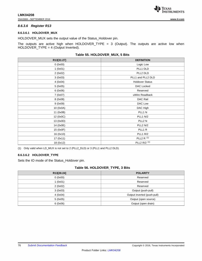
76
LMK04208SNAS684 –SEPTEMBER 2016 www.ti.com
Product Folder Links: LMK04208
Submit Documentation Feedback Copyright © 2016, Texas Instruments Incorporated
(1) Only valid when LD_MUX is not set to 2 (PLL2_DLD) or 3 (PLL1 and PLL2 DLD).
8.6.3.6 Register R13
8.6.3.6.1 HOLDOVER_MUX
HOLDOVER_MUX sets the output value of the Status_Holdover pin.
The outputs are active high when HOLDOVER_TYPE = 3 (Output). The outputs are active low whenHOLDOVER_TYPE = 4 (Output Inverted).
Table 55. HOLDOVER_MUX, 5 BitsR13[31:27] DEFINITION
0 (0x00) Logic Low1 (0x01) PLL1 DLD2 (0x02) PLL2 DLD3 (0x03) PLL1 and PLL2 DLD4 (0x04) Holdover Status5 (0x05) DAC Locked6 (0x06) Reserved7 (0x07) uWire Readback8 (0x08) DAC Rail9 (0x09) DAC Low
10 (0x0A) DAC High11 (0x0B) PLL1 N12 (0x0C) PLL1 N/213 (0x0D) PLL2 N14 (0x0E) PLL2 N/215 (0x0F) PLL1 R16 (0x10) PLL1 R/217 (0x11) PLL2 R (1)
18 (0x12) PLL2 R/2 (1)
8.6.3.6.2 HOLDOVER_TYPE
Sets the IO mode of the Status_Holdover pin.
Table 56. HOLDOVER_TYPE, 3 BitsR13[26:24] POLARITY
0 (0x00) Reserved1 (0x01) Reserved2 (0x02) Reserved3 (0x03) Output (push-pull)4 (0x04) Output inverted (push-pull)5 (0x05) Output (open source)6 (0x06) Output (open drain)
77
LMK04208www.ti.com SNAS684 –SEPTEMBER 2016
Product Folder Links: LMK04208
Submit Documentation FeedbackCopyright © 2016, Texas Instruments Incorporated
8.6.3.6.3 Status_CLKin1_MUX
Status_CLKin1_MUX sets the output value of the Status_CLKin1 pin. If Status_CLKin1_TYPE is set to an inputtype, this register has no effect. This MUX register only sets the output signal.
The outputs are active high when Status_CLKin1_TYPE = 3 (Output). The outputs are active low whenStatus_CLKin1_TYPE = 4 (Output Inverted).
Table 57. Status_CLKin1_MUX, 3 BitsR13[22:20] DEFINITION
0 (0x00) Logic Low1 (0x01) CLKin1 LOS2 (0x02) CLKin1 Selected3 (0x03) DAC Locked4 (0x04) DAC Low5 (0x05) DAC High6 (0x06) uWire Readback
8.6.3.6.4 Status_CLKin0_TYPE
Status_CLKin0_TYPE sets the IO type of the Status_CLKin0 pin.
Table 58. Status_CLKin0_TYPE, 3 BitsR13[18:16] DEFINITION
0 (0x00) Input1 (0x01) Input w/ pull-up resistor2 (0x02) Input w/ pull-down resistor3 (0x03) Output (push-pull)4 (0x04) Output inverted (push-pull)5 (0x05) Output (open source)6 (0x06) Output (open drain)
8.6.3.6.5 DISABLE_DLD1_DET
DISABLE_DLD1_DET disables the HOLDOVER mode from being activated when PLL1 lock detect signaltransitions from high to low.
When using Pin Select Mode as the input clock switch mode, this bit should normally be set.
Table 59. DISABLE_DLD1_DETR13[15] HOLDOVER DLD1 DETECT
0 PLL1 DLD causes clock switch event1 PLL1 DLD does not cause clock switch event
78
LMK04208SNAS684 –SEPTEMBER 2016 www.ti.com
Product Folder Links: LMK04208
Submit Documentation Feedback Copyright © 2016, Texas Instruments Incorporated
8.6.3.6.6 Status_CLKin0_MUX
CLKin0_MUX sets the output value of the Status_CLKin0 pin. If Status_CLKin0_TYPE is set to an input type, thisregister has no effect. This MUX register only sets the output signal.
The outputs logic is active high when Status_CLKin0_TYPE = 3 (Output). The outputs logic is active low whenStatus_CLKin0_TYPE = 4 (Output Inverted).
Table 60. Status_CLKin0_MUX, 3 BitsR13[14:12] DEFINITION
0 (0x00) Logic Low1 (0x01) CLKin0 LOS2 (0x02) CLKin0 Selected3 (0x03) DAC Locked4 (0x04) DAC Low5 (0x05) DAC High6 (0x06) uWire Readback
8.6.3.6.7 CLKin_SELECT_MODE
CLKin_SELECT_MODE sets the mode used in determining reference CLKin for PLL1.
Table 61. CLKin_SELECT_MODE, 3 BitsR13[11:9] MODE0 (0x00) CLKin0 Manual1 (0x01) CLKin1 Manual2 (0x02) Reserved3 (0x03) Pin Select Mode4 (0x04) Auto Mode5 (0x05) Reserved6 (0x06) Auto mode and next clock pin select7 (0x07) Reserved
8.6.3.6.8 CLKin_Sel_INV
CLKin_Sel_INV sets the input polarity of Status_CLKin0 and Status_CLKin1 pins.
Inversion for Status 0 and 1 pins is only valid for CLKin_SELECT_MODE = 0x06.
Table 62. CLKin_Sel_INVR13[8] INPUT
0 Active High1 Active Low
79
LMK04208www.ti.com SNAS684 –SEPTEMBER 2016
Product Folder Links: LMK04208
Submit Documentation FeedbackCopyright © 2016, Texas Instruments Incorporated
8.6.3.6.9 EN_CLKinX
Each clock input can individually be enabled to be used during auto-switching CLKin_SELECT_MODE. Clockinput switching priority is always CLKin0 → CLKin1.
Table 63. EN_CLKin1R13[6] ENABLED
0 No1 Yes
Table 64. EN_CLKin0R13[5] ENABLED
0 No1 Yes
8.6.3.7 Register 14
8.6.3.7.1 LOS_TIMEOUT
This bit controls the amount of time in which no activity on a CLKin causes LOS (Loss-of-Signal) to be asserted.
Table 65. LOS_TIMEOUT, 2 BitsR14[31:30] TIMEOUT
0 (0x00) 1200 ns, 420 kHz1 (0x01) 206 ns, 2.5 MHz2 (0x02) 52.9 ns, 10 MHz3 (0x03) 23.7 ns, 22 MHz
8.6.3.7.2 EN_LOS
Enables the LOS (Loss-of-Signal) timeout control.
Table 66. EN_LOSR14[28] LOS
0 Disabled1 Enabled
8.6.3.7.3 Status_CLKin1_TYPE
Sets the IO type of the Status_CLKin1 pin.
Table 67. Status_CLKin1_TYPE, 3 BitsR14[26:24] POLARITY
0 (0x00) Input1 (0x01) Input w/ pull-up resistor2 (0x02) Input w/ pull-down resistor3 (0x03) Output (push-pull)4 (0x04) Output inverted (push-pull)5 (0x05) Output (open source)6 (0x06) Output (open drain)
80
LMK04208SNAS684 –SEPTEMBER 2016 www.ti.com
Product Folder Links: LMK04208
Submit Documentation Feedback Copyright © 2016, Texas Instruments Incorporated
8.6.3.7.4 CLKinX_BUF_TYPE, PLL1 CLKinX/CLKinX* Buffer Type
There are two input buffer types for the PLL1 reference clock inputs: either bipolar or CMOS. Bipolar isrecommended for differential inputs such as LVDS and LVPECL. CMOS is recommended for DC coupled singleended inputs.
When using bipolar, CLKinX and CLKinX* input pins must be AC coupled when using a differential or singleended input.
When using CMOS, CLKinX and CLKinX* input pins may be AC or DC coupled with a differential input.
When using CMOS in single ended mode, the unused clock input pin (CLKinX or CLKinX*) must be ACgrounded. The used clock input pin (CLKinX* or CLKinX) may be AC or DC coupled to the signal source.
The programming addresses table shows at what register and address the specified CLKinX_BUF_TYPE bit islocated.
The CLKinX_BUF_TYPE table shows the programming definition for these registers.
Table 68. CLKinX_BUF_TYPE Programming AddressesCLKinX_BUF_TYPE PROGRAMMING ADDRESSCLKin1_BUF_TYPE R14[21]CLKin0_BUF_TYPE R14[20]
Table 69. CLKinX_BUF_TYPER14[21, 20] CLKinX BUFFER TYPE
0 Bipolar1 CMOS
8.6.3.7.5 DAC_HIGH_TRIP
Voltage from Vcc at which holdover mode is entered if EN_VTUNE_RAIL_DAC is enabled. This will also set flagswhich can be monitored out Status_LD/Status_Holdover pins.
Step size is ~51 mV.
Table 70. DAC_HIGH_TRIP, 6 BitsR14[19:14] TRIP VOLTAGE FROM VCC (V)
0 (0x00) 1 × Vcc / 641 (0x01) 2 × Vcc / 642 (0x02) 3 × Vcc / 643 (0x03) 4 × Vcc / 644 (0x04) 5 × Vcc / 64
... ...61 (0x3D) 62 × Vcc / 6462 (0x3E) 63 × Vcc / 6463 (0x3F) 64 × Vcc / 64
81
LMK04208www.ti.com SNAS684 –SEPTEMBER 2016
Product Folder Links: LMK04208
Submit Documentation FeedbackCopyright © 2016, Texas Instruments Incorporated
8.6.3.7.6 DAC_LOW_TRIP
Voltage from GND at which holdover mode is entered if EN_VTUNE_RAIL_DAC is enabled. This will also setflags which can be monitored out Status_LD/Status_Holdover pins.
Step size is ~51 mV
Table 71. DAC_LOW_TRIP, 6 BitsR14[11:6] TRIP VOLTAGE from GND (V)0 (0x00) 1 × Vcc / 641 (0x01) 2 × Vcc / 642 (0x02) 3 × Vcc / 643 (0x03) 4 × Vcc / 644 (0x04) 5 × Vcc / 64
... ...61 (0x3D) 62 × Vcc / 6462 (0x3E) 63 × Vcc / 6463 (0x3F) 64 × Vcc / 64
8.6.3.7.7 EN_VTUNE_RAIL_DET
Enables the DAC Vtune rail detection. When the DAC achieves a specified Vtune, if this bit is enabled, thecurrent clock input is considered invalid and an input clock switch event is generated.
Table 72. EN_VTUNE_RAIL_DETR14[5] STATE
0 Disabled1 Enabled

82
LMK04208SNAS684 –SEPTEMBER 2016 www.ti.com
Product Folder Links: LMK04208
Submit Documentation Feedback Copyright © 2016, Texas Instruments Incorporated
8.6.3.8 Register 15
8.6.3.8.1 MAN_DAC
Sets the DAC value when in manual DAC mode in ~3.2 mV steps.
Table 73. MAN_DAC, 10 BitsR15[31:22] DAC VOLTAGE
0 (0x00) 0 × Vcc / 10231 (0x01) 1 × Vcc / 10232 (0x02) 2 × Vcc / 1023
... ...1023 (0x3FF) 1023 × Vcc / 1023
8.6.3.8.2 EN_MAN_DAC
This bit enables the manual DAC mode.
Table 74. EN_MAN_DACR15[20] DAC MODE
0 Automatic1 Manual
8.6.3.8.3 HOLDOVER_DLD_CNT
Lock must be valid for this many clocks of PLL1 PDF before holdover mode is exited.
Table 75. HOLDOVER_DLD_CNT, 14 BitsR15[19:6] EXIT COUNTS0 (0x00) Reserved1 (0x01) 12 (0x02) 2
... ...16,383 (0x3FFF) 16,383
8.6.3.8.4 FORCE_HOLDOVER
This bit forces the holdover mode.
When holdover is forced, if in fixed CPout1 mode (EN_TRACK = 0 or 1, EN_MAN_DAC = 1) , then the DAC willset the programmed MAN_DAC value. If in tracked CPout1 mode (EN_TRACK = 1, EN_MAN_DAC = 0,EN_VTUNE_RAIL_DET = 0), then the DAC will set the current tracked DAC value.
Setting FORCE_HOLDOVER does not constitute a clock input switch event unless DISABLE_DLD1_DET = 0,since when in holdover mode, PLL1_DLD = 0 will trigger the clock input switch event.
Table 76. FORCE_HOLDOVERR15[5] HOLDOVER
0 Disabled1 Enabled
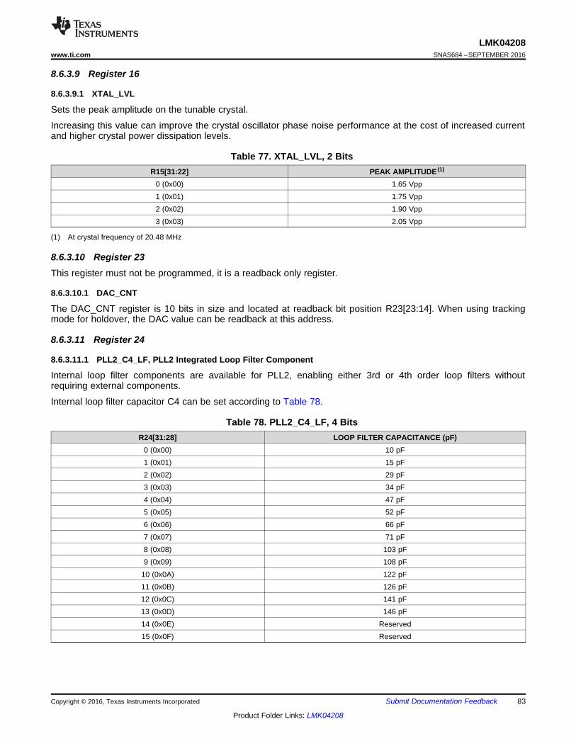
83
LMK04208www.ti.com SNAS684 –SEPTEMBER 2016
Product Folder Links: LMK04208
Submit Documentation FeedbackCopyright © 2016, Texas Instruments Incorporated
(1) At crystal frequency of 20.48 MHz
8.6.3.9 Register 16
8.6.3.9.1 XTAL_LVL
Sets the peak amplitude on the tunable crystal.
Increasing this value can improve the crystal oscillator phase noise performance at the cost of increased currentand higher crystal power dissipation levels.
Table 77. XTAL_LVL, 2 BitsR15[31:22] PEAK AMPLITUDE (1)
0 (0x00) 1.65 Vpp1 (0x01) 1.75 Vpp2 (0x02) 1.90 Vpp3 (0x03) 2.05 Vpp
8.6.3.10 Register 23This register must not be programmed, it is a readback only register.
8.6.3.10.1 DAC_CNT
The DAC_CNT register is 10 bits in size and located at readback bit position R23[23:14]. When using trackingmode for holdover, the DAC value can be readback at this address.
8.6.3.11 Register 24
8.6.3.11.1 PLL2_C4_LF, PLL2 Integrated Loop Filter Component
Internal loop filter components are available for PLL2, enabling either 3rd or 4th order loop filters withoutrequiring external components.
Internal loop filter capacitor C4 can be set according to Table 78.
Table 78. PLL2_C4_LF, 4 BitsR24[31:28] LOOP FILTER CAPACITANCE (pF)
0 (0x00) 10 pF1 (0x01) 15 pF2 (0x02) 29 pF3 (0x03) 34 pF4 (0x04) 47 pF5 (0x05) 52 pF6 (0x06) 66 pF7 (0x07) 71 pF8 (0x08) 103 pF9 (0x09) 108 pF
10 (0x0A) 122 pF11 (0x0B) 126 pF12 (0x0C) 141 pF13 (0x0D) 146 pF14 (0x0E) Reserved15 (0x0F) Reserved
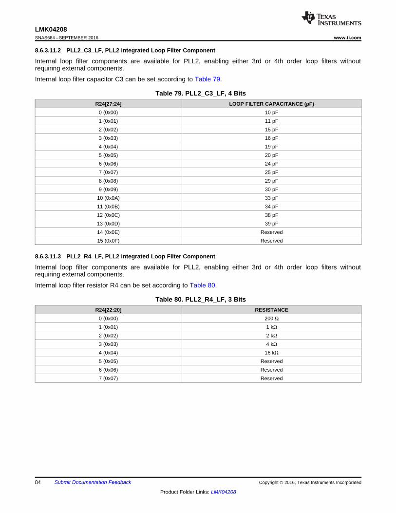
84
LMK04208SNAS684 –SEPTEMBER 2016 www.ti.com
Product Folder Links: LMK04208
Submit Documentation Feedback Copyright © 2016, Texas Instruments Incorporated
8.6.3.11.2 PLL2_C3_LF, PLL2 Integrated Loop Filter Component
Internal loop filter components are available for PLL2, enabling either 3rd or 4th order loop filters withoutrequiring external components.
Internal loop filter capacitor C3 can be set according to Table 79.
Table 79. PLL2_C3_LF, 4 BitsR24[27:24] LOOP FILTER CAPACITANCE (pF)
0 (0x00) 10 pF1 (0x01) 11 pF2 (0x02) 15 pF3 (0x03) 16 pF4 (0x04) 19 pF5 (0x05) 20 pF6 (0x06) 24 pF7 (0x07) 25 pF8 (0x08) 29 pF9 (0x09) 30 pF
10 (0x0A) 33 pF11 (0x0B) 34 pF12 (0x0C) 38 pF13 (0x0D) 39 pF14 (0x0E) Reserved15 (0x0F) Reserved
8.6.3.11.3 PLL2_R4_LF, PLL2 Integrated Loop Filter Component
Internal loop filter components are available for PLL2, enabling either 3rd or 4th order loop filters withoutrequiring external components.
Internal loop filter resistor R4 can be set according to Table 80.
Table 80. PLL2_R4_LF, 3 BitsR24[22:20] RESISTANCE
0 (0x00) 200 Ω
1 (0x01) 1 kΩ2 (0x02) 2 kΩ3 (0x03) 4 kΩ4 (0x04) 16 kΩ5 (0x05) Reserved6 (0x06) Reserved7 (0x07) Reserved
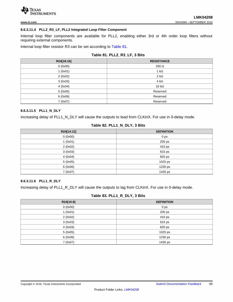
85
LMK04208www.ti.com SNAS684 –SEPTEMBER 2016
Product Folder Links: LMK04208
Submit Documentation FeedbackCopyright © 2016, Texas Instruments Incorporated
8.6.3.11.4 PLL2_R3_LF, PLL2 Integrated Loop Filter Component
Internal loop filter components are available for PLL2, enabling either 3rd or 4th order loop filters withoutrequiring external components.
Internal loop filter resistor R3 can be set according to Table 81.
Table 81. PLL2_R3_LF, 3 BitsR24[18:16] RESISTANCE
0 (0x00) 200 Ω
1 (0x01) 1 kΩ2 (0x02) 2 kΩ3 (0x03) 4 kΩ4 (0x04) 16 kΩ5 (0x05) Reserved6 (0x06) Reserved7 (0x07) Reserved
8.6.3.11.5 PLL1_N_DLY
Increasing delay of PLL1_N_DLY will cause the outputs to lead from CLKinX. For use in 0-delay mode.
Table 82. PLL1_N_DLY, 3 BitsR24[14:12] DEFINITION
0 (0x00) 0 ps1 (0x01) 205 ps2 (0x02) 410 ps3 (0x03) 615 ps4 (0x04) 820 ps5 (0x05) 1025 ps6 (0x06) 1230 ps7 (0x07) 1435 ps
8.6.3.11.6 PLL1_R_DLY
Increasing delay of PLL1_R_DLY will cause the outputs to lag from CLKinX. For use in 0-delay mode.
Table 83. PLL1_R_DLY, 3 BitsR24[10:8] DEFINITION0 (0x00) 0 ps1 (0x01) 205 ps2 (0x02) 410 ps3 (0x03) 615 ps4 (0x04) 820 ps5 (0x05) 1025 ps6 (0x06) 1230 ps7 (0x07) 1435 ps
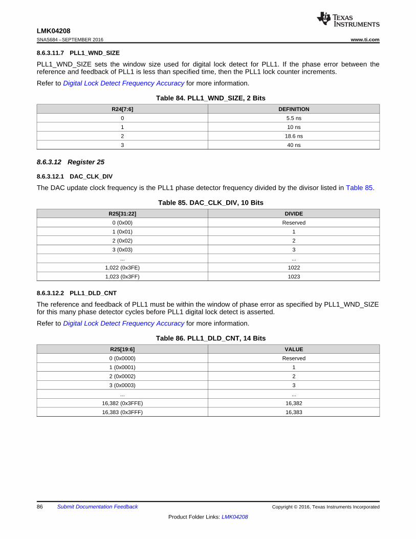
86
LMK04208SNAS684 –SEPTEMBER 2016 www.ti.com
Product Folder Links: LMK04208
Submit Documentation Feedback Copyright © 2016, Texas Instruments Incorporated
8.6.3.11.7 PLL1_WND_SIZE
PLL1_WND_SIZE sets the window size used for digital lock detect for PLL1. If the phase error between thereference and feedback of PLL1 is less than specified time, then the PLL1 lock counter increments.
Refer to Digital Lock Detect Frequency Accuracy for more information.
Table 84. PLL1_WND_SIZE, 2 BitsR24[7:6] DEFINITION
0 5.5 ns1 10 ns2 18.6 ns3 40 ns
8.6.3.12 Register 25
8.6.3.12.1 DAC_CLK_DIV
The DAC update clock frequency is the PLL1 phase detector frequency divided by the divisor listed in Table 85.
Table 85. DAC_CLK_DIV, 10 BitsR25[31:22] DIVIDE
0 (0x00) Reserved1 (0x01) 12 (0x02) 23 (0x03) 3
... ...1,022 (0x3FE) 10221,023 (0x3FF) 1023
8.6.3.12.2 PLL1_DLD_CNT
The reference and feedback of PLL1 must be within the window of phase error as specified by PLL1_WND_SIZEfor this many phase detector cycles before PLL1 digital lock detect is asserted.
Refer to Digital Lock Detect Frequency Accuracy for more information.
Table 86. PLL1_DLD_CNT, 14 BitsR25[19:6] VALUE0 (0x0000) Reserved1 (0x0001) 12 (0x0002) 23 (0x0003) 3
... ...16,382 (0x3FFE) 16,38216,383 (0x3FFF) 16,383
87
LMK04208www.ti.com SNAS684 –SEPTEMBER 2016
Product Folder Links: LMK04208
Submit Documentation FeedbackCopyright © 2016, Texas Instruments Incorporated
8.6.3.13 Register 26
8.6.3.13.1 PLL2_WND_SIZE
PLL2_WND_SIZE sets the window size used for digital lock detect for PLL2. If the phase error between thereference and feedback of PLL2 is less than specified time, then the PLL2 lock counter increments. This valuemust be programmed to 2 (3.7 ns).
Refer to Digital Lock Detect Frequency Accuracy for more information.
Table 87. PLL2_WND_SIZE, 2 BitsR26[31:30] DEFINITION
0 (0x00) Reserved1 (0x01) Reserved2 (0x02) 3.7 ns3 (0x03) Reserved
(1) When the doubler is not enabled, PLL2_R should not be programmed to 1.(2) See PLL2 Frequency Doubler
8.6.3.13.2 EN_PLL2_REF_2X, PLL2 Reference Frequency Doubler
Enabling the PLL2 reference frequency doubler allows for higher phase detector frequencies on PLL2 than wouldnormally be allowed with the given VCXO or Crystal frequency.
Higher phase detector frequencies reduces the PLL N values which makes the design of wider loop bandwidthfilters possible.
Table 88. EN_PLL2_REF_2XR26[29] DESCRIPTION
0 Reference frequency normal (1)
1 Reference frequency doubled (2x) (2)
8.6.3.13.3 PLL2_CP_POL, PLL2 Charge Pump Polarity
PLL2_CP_POL sets the charge pump polarity for PLL2. The internal VCO requires the negative charge pumppolarity to be selected. Many VCOs use positive slope.
A positive slope VCO increases output frequency with increasing voltage. A negative slope VCO decreasesoutput frequency with increasing voltage.
Table 89. PLL2_CP_POLR26[28] DESCRIPTION
0 Negative Slope VCO/VCXO1 Positive Slope VCO/VCXO
88
LMK04208SNAS684 –SEPTEMBER 2016 www.ti.com
Product Folder Links: LMK04208
Submit Documentation Feedback Copyright © 2016, Texas Instruments Incorporated
8.6.3.13.4 PLL2_CP_GAIN, PLL2 Charge Pump Current
This bit programs the PLL2 charge pump output current level. Table 90 also illustrates the impact of the PLL2TRI-STATE bit in conjunction with PLL2_CP_GAIN.
Table 90. PLL2_CP_GAIN, 2 Bits
R26[27:26] PLL2_CP_TRIR26[5] CHARGE PUMP CURRENT (µA)
X 1 Hi-Z0 (0x00) 0 1001 (0x01) 0 4002 (0x02) 0 16003 (0x03) 0 3200
8.6.3.13.5 PLL2_DLD_CNT
The reference and feedback of PLL2 must be within the window of phase error as specified by PLL2_WND_SIZEfor PLL2_DLD_CNT cycles before PLL2 digital lock detect is asserted.
Refer to Digital Lock Detect Frequency Accuracy for more information
Table 91. PLL2_DLD_CNT, 14 BitsR26[19:6] VALUE0 (0x00) Reserved1 (0x01) 12 (0x02) 23 (0x003) 3
... ...16,382 (0x3FFE) 16,38216,383 (0x3FFF) 16,383
8.6.3.13.6 PLL2_CP_TRI, PLL2 Charge Pump TRI-STATE
This bit allows for the PLL2 charge pump output pin, CPout2, to be placed into TRI-STATE.
Table 92. PLL2_CP_TRIR26[5] DESCRIPTION
0 PLL2 CPout2 is active1 PLL2 CPout2 is at TRI-STATE
89
LMK04208www.ti.com SNAS684 –SEPTEMBER 2016
Product Folder Links: LMK04208
Submit Documentation FeedbackCopyright © 2016, Texas Instruments Incorporated
8.6.3.14 Register 27
8.6.3.14.1 PLL1_CP_POL, PLL1 Charge Pump Polarity
PLL1_CP_POL sets the charge pump polarity for PLL1. Many VCXOs use positive slope.
A positive slope VCXO increases output frequency with increasing voltage. A negative slope VCXO decreasesoutput frequency with increasing voltage.
Table 93. PLL1_CP_POLR27[28] DESCRIPTION
0 Negative Slope VCO/VCXO1 Positive Slope VCO/VCXO
8.6.3.14.2 PLL1_CP_GAIN, PLL1 Charge Pump Current
This bit programs the PLL1 charge pump output current level. Table 94 also illustrates the impact of the PLL1TRI-STATE bit in conjunction with PLL1_CP_GAIN.
Table 94. PLL1_CP_GAIN, 2 Bits
R26[27:26] PLL1_CP_TRIR27[5] CHARGE PUMP CURRENT (µA)
X 1 Hi-Z0 (0x00) 0 1001 (0x01) 0 2002 (0x02) 0 4003 (0x03) 0 1600
8.6.3.14.3 CLKinX_PreR_DIV
The pre-R dividers before the PLL1 R divider can be programmed such that when the active clock input isswitched, the frequency at the input of the PLL1 R divider will be the same. This allows PLL1 to stay in lockwithout needing to re-program the PLL1 R register when different clock input frequencies are used. This isespecially useful in the auto CLKin switching modes.
Table 95. CLKinX_PreR_DIV Programming AddressesCLKinX_PreR_DIV PROGRAMMING ADDRESSCLKin1_PreR_DIV R27[23:22]CLKin0_PreR_DIV R27[21:20]
Table 96. CLKinX_PreR_DIV, 2 BitsR27[23:22, 21:20] DIVIDE
0 (0x00) 11 (0x01) 22 (0x02) 43 (0x03) 8
90
LMK04208SNAS684 –SEPTEMBER 2016 www.ti.com
Product Folder Links: LMK04208
Submit Documentation Feedback Copyright © 2016, Texas Instruments Incorporated
8.6.3.14.4 PLL1_R, PLL1 R Divider
The reference path into the PLL1 phase detector includes the PLL1 R divider. Refer to PLL Programming formore information on how to program the PLL dividers to lock the PLL.
The valid values for PLL1_R are shown in Table 97.
Table 97. PLL1_R, 14 BitsR27[19:6] DIVIDE0 (0x00) Reserved1 (0x01) 12 (0x02) 23 (0x03) 3
... ...16,382 (0x3FFE) 16,38216,383 (0x3FFF) 16,383
8.6.3.14.5 PLL1_CP_TRI, PLL1 Charge Pump TRI-STATE
This bit allows for the PLL1 charge pump output pin, CPout1, to be placed into TRI-STATE.
Table 98. PLL1_CP_TRIR27[5] DESCRIPTION
0 PLL1 CPout1 is active1 PLL1 CPout1 is at TRI-STATE
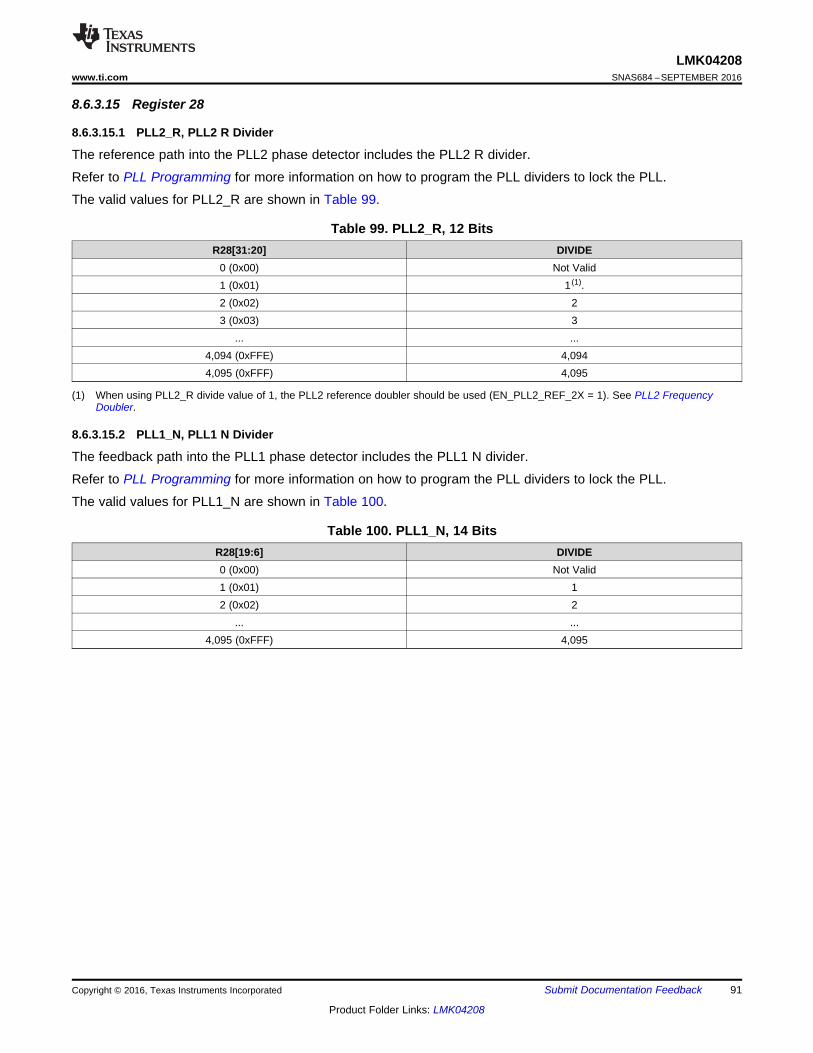
91
LMK04208www.ti.com SNAS684 –SEPTEMBER 2016
Product Folder Links: LMK04208
Submit Documentation FeedbackCopyright © 2016, Texas Instruments Incorporated
(1) When using PLL2_R divide value of 1, the PLL2 reference doubler should be used (EN_PLL2_REF_2X = 1). See PLL2 FrequencyDoubler.
8.6.3.15 Register 28
8.6.3.15.1 PLL2_R, PLL2 R Divider
The reference path into the PLL2 phase detector includes the PLL2 R divider.
Refer to PLL Programming for more information on how to program the PLL dividers to lock the PLL.
The valid values for PLL2_R are shown in Table 99.
Table 99. PLL2_R, 12 BitsR28[31:20] DIVIDE
0 (0x00) Not Valid1 (0x01) 1 (1).2 (0x02) 23 (0x03) 3
... ...4,094 (0xFFE) 4,0944,095 (0xFFF) 4,095
8.6.3.15.2 PLL1_N, PLL1 N Divider
The feedback path into the PLL1 phase detector includes the PLL1 N divider.
Refer to PLL Programming for more information on how to program the PLL dividers to lock the PLL.
The valid values for PLL1_N are shown in Table 100.
Table 100. PLL1_N, 14 BitsR28[19:6] DIVIDE0 (0x00) Not Valid1 (0x01) 12 (0x02) 2
... ...4,095 (0xFFF) 4,095
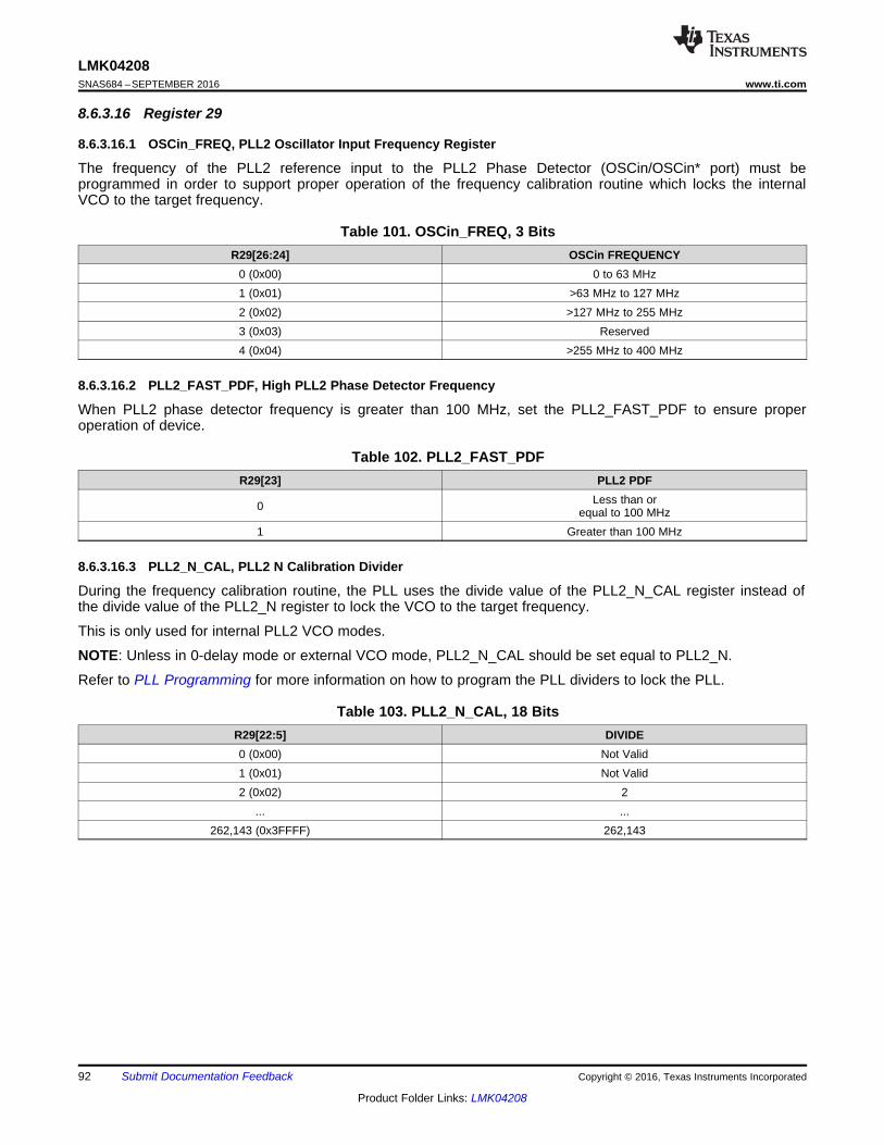
92
LMK04208SNAS684 –SEPTEMBER 2016 www.ti.com
Product Folder Links: LMK04208
Submit Documentation Feedback Copyright © 2016, Texas Instruments Incorporated
8.6.3.16 Register 29
8.6.3.16.1 OSCin_FREQ, PLL2 Oscillator Input Frequency Register
The frequency of the PLL2 reference input to the PLL2 Phase Detector (OSCin/OSCin* port) must beprogrammed in order to support proper operation of the frequency calibration routine which locks the internalVCO to the target frequency.
Table 101. OSCin_FREQ, 3 BitsR29[26:24] OSCin FREQUENCY
0 (0x00) 0 to 63 MHz1 (0x01) >63 MHz to 127 MHz2 (0x02) >127 MHz to 255 MHz3 (0x03) Reserved4 (0x04) >255 MHz to 400 MHz
8.6.3.16.2 PLL2_FAST_PDF, High PLL2 Phase Detector Frequency
When PLL2 phase detector frequency is greater than 100 MHz, set the PLL2_FAST_PDF to ensure properoperation of device.
Table 102. PLL2_FAST_PDFR29[23] PLL2 PDF
0 Less than orequal to 100 MHz
1 Greater than 100 MHz
8.6.3.16.3 PLL2_N_CAL, PLL2 N Calibration Divider
During the frequency calibration routine, the PLL uses the divide value of the PLL2_N_CAL register instead ofthe divide value of the PLL2_N register to lock the VCO to the target frequency.
This is only used for internal PLL2 VCO modes.
NOTE: Unless in 0-delay mode or external VCO mode, PLL2_N_CAL should be set equal to PLL2_N.
Refer to PLL Programming for more information on how to program the PLL dividers to lock the PLL.
Table 103. PLL2_N_CAL, 18 BitsR29[22:5] DIVIDE0 (0x00) Not Valid1 (0x01) Not Valid2 (0x02) 2
... ...262,143 (0x3FFFF) 262,143
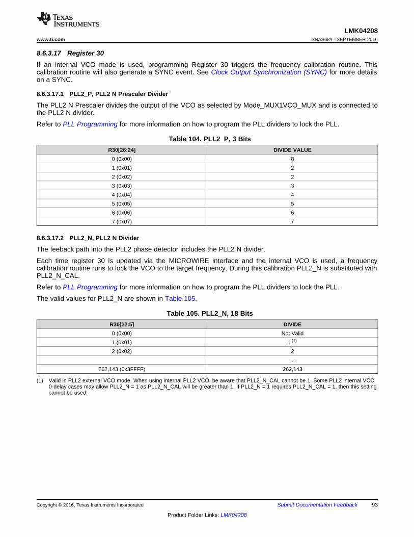
93
LMK04208www.ti.com SNAS684 –SEPTEMBER 2016
Product Folder Links: LMK04208
Submit Documentation FeedbackCopyright © 2016, Texas Instruments Incorporated
8.6.3.17 Register 30If an internal VCO mode is used, programming Register 30 triggers the frequency calibration routine. Thiscalibration routine will also generate a SYNC event. See Clock Output Synchronization (SYNC) for more detailson a SYNC.
8.6.3.17.1 PLL2_P, PLL2 N Prescaler Divider
The PLL2 N Prescaler divides the output of the VCO as selected by Mode_MUX1VCO_MUX and is connected tothe PLL2 N divider.
Refer to PLL Programming for more information on how to program the PLL dividers to lock the PLL.
Table 104. PLL2_P, 3 BitsR30[26:24] DIVIDE VALUE
0 (0x00) 81 (0x01) 22 (0x02) 23 (0x03) 34 (0x04) 45 (0x05) 56 (0x06) 67 (0x07) 7
(1) Valid in PLL2 external VCO mode. When using internal PLL2 VCO, be aware that PLL2_N_CAL cannot be 1. Some PLL2 internal VCO0-delay cases may allow PLL2_N = 1 as PLL2_N_CAL will be greater than 1. If PLL2_N = 1 requires PLL2_N_CAL = 1, then this settingcannot be used.
8.6.3.17.2 PLL2_N, PLL2 N Divider
The feeback path into the PLL2 phase detector includes the PLL2 N divider.
Each time register 30 is updated via the MICROWIRE interface and the internal VCO is used, a frequencycalibration routine runs to lock the VCO to the target frequency. During this calibration PLL2_N is substituted withPLL2_N_CAL.
Refer to PLL Programming for more information on how to program the PLL dividers to lock the PLL.
The valid values for PLL2_N are shown in Table 105.
Table 105. PLL2_N, 18 BitsR30[22:5] DIVIDE0 (0x00) Not Valid1 (0x01) 1 (1)
2 (0x02) 2...
262,143 (0x3FFFF) 262,143
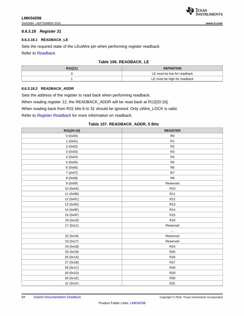
94
LMK04208SNAS684 –SEPTEMBER 2016 www.ti.com
Product Folder Links: LMK04208
Submit Documentation Feedback Copyright © 2016, Texas Instruments Incorporated
8.6.3.18 Register 31
8.6.3.18.1 READBACK_LE
Sets the required state of the LEuWire pin when performing register readback.
Refer to Readback.
Table 106. READBACK_LER31[21] DEFINITION
0 LE must be low for readback1 LE must be high for readback
8.6.3.18.2 READBACK_ADDR
Sets the address of the register to read back when performing readback.
When reading register 12, the READBACK_ADDR will be read back at R12[20:16].
When reading back from R31 bits 6 to 31 should be ignored. Only uWire_LOCK is valid.
Refer to Register Readback for more information on readback.
Table 107. READBACK_ADDR, 5 BitsR31[20:16] REGISTER
0 (0x00) R01 (0x01) R12 (0x02) R23 (0x03) R34 (0x04) R45 (0x05) R56 (0x06) R67 (0x07) R78 (0x08) R89 (0x09) Reserved
10 (0x0A) R1011 (0x0B) R1112 (0x0C) R1213 (0x0D) R1314 (0x0E) R1415 (0x0F) R1516 (0x10) R1617 (0x11) Reserved
... ...22 (0x16) Reserved23 (0x17) Reserved24 (0x18) R2425 (0x19) R2526 (0x1A) R2627 (0x1B) R2728 (0x1C) R2829 (0x1D) R2930 (0x1E) R3031 (0x1F) R31
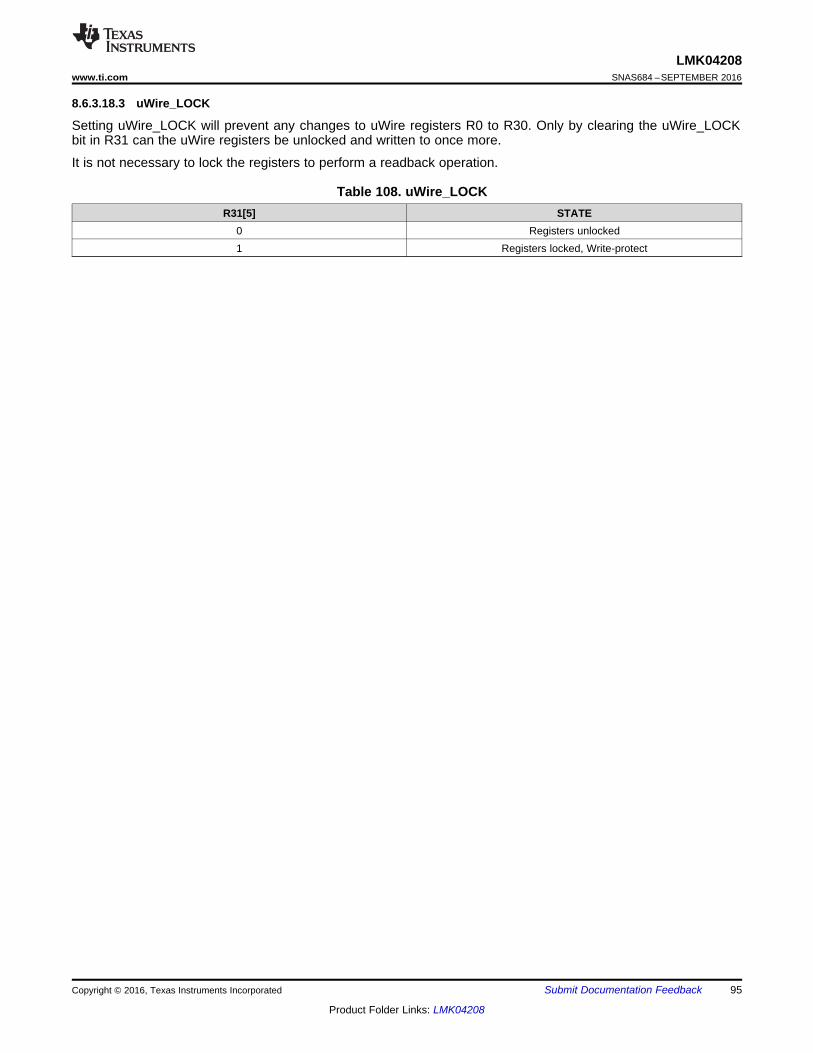
95
LMK04208www.ti.com SNAS684 –SEPTEMBER 2016
Product Folder Links: LMK04208
Submit Documentation FeedbackCopyright © 2016, Texas Instruments Incorporated
8.6.3.18.3 uWire_LOCK
Setting uWire_LOCK will prevent any changes to uWire registers R0 to R30. Only by clearing the uWire_LOCKbit in R31 can the uWire registers be unlocked and written to once more.
It is not necessary to lock the registers to perform a readback operation.
Table 108. uWire_LOCKR31[5] STATE
0 Registers unlocked1 Registers locked, Write-protect
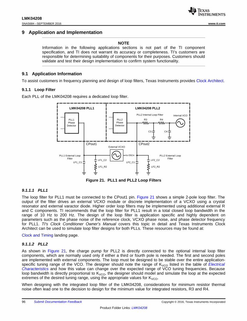
PLL2 Phase
Detector
C4
R3 R4
LMK04208 PLL2
PLL2 Internal Loop Filter
PLL2 External Loop Filter
LMK04208 PLL1
PLL1 External Loop Filter
CPout2External VCXO
Internal VCO
C3
PLL1Phase
Detector
LF1_C2
LF1_R2
LF1_C1
CPout1
LF2_C2
LF2_R2
LF2_C1
to OSCin
96
LMK04208SNAS684 –SEPTEMBER 2016 www.ti.com
Product Folder Links: LMK04208
Submit Documentation Feedback Copyright © 2016, Texas Instruments Incorporated
9 Application and Implementation
NOTEInformation in the following applications sections is not part of the TI componentspecification, and TI does not warrant its accuracy or completeness. TI’s customers areresponsible for determining suitability of components for their purposes. Customers shouldvalidate and test their design implementation to confirm system functionality.
9.1 Application InformationTo assist customers in frequency planning and design of loop filters, Texas Instruments provides Clock Architect.
9.1.1 Loop FilterEach PLL of the LMK04208 requires a dedicated loop filter.
Figure 21. PLL1 and PLL2 Loop Filters
9.1.1.1 PLL1The loop filter for PLL1 must be connected to the CPout1 pin. Figure 21 shows a simple 2-pole loop filter. Theoutput of the filter drives an external VCXO module or discrete implementation of a VCXO using a crystalresonator and external varactor diode. Higher order loop filters may be implemented using additional external Rand C components. TI recommends that the loop filter for PLL1 result in a total closed loop bandwidth in therange of 10 Hz to 200 Hz. The design of the loop filter is application specific and highly dependent onparameters such as the phase noise of the reference clock, VCXO phase noise, and phase detector frequencyfor PLL1. TI's Clock Conditioner Owner’s Manual covers this topic in detail and Texas Instruments ClockArchitect can be used to simulate loop filter designs for both PLLs. These resources may be found at:
Clock and Timing landing page.
9.1.1.2 PLL2As shown in Figure 21, the charge pump for PLL2 is directly connected to the optional internal loop filtercomponents, which are normally used only if either a third or fourth pole is needed. The first and second polesare implemented with external components. The loop must be designed to be stable over the entire application-specific tuning range of the VCO. The designer should note the range of KVCO listed in the table of ElectricalCharacteristics and how this value can change over the expected range of VCO tuning frequencies. Becauseloop bandwidth is directly proportional to KVCO, the designer should model and simulate the loop at the expectedextremes of the desired tuning range, using the appropriate values for KVCO.
When designing with the integrated loop filter of the LMK04208, considerations for minimum resistor thermalnoise often lead one to the decision to design for the minimum value for integrated resistors, R3 and R4.
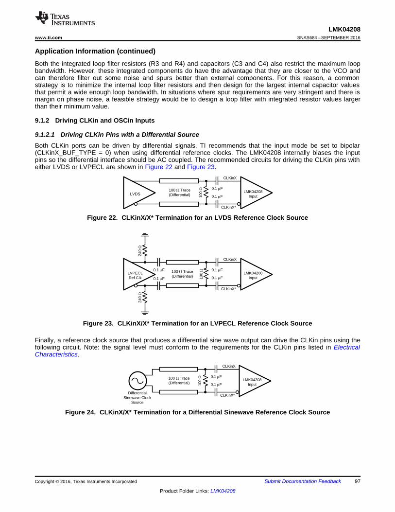
0.1 PF
0.1 PFLMK04208
Input100 :100 :Trace
(Differential)
Differential Sinewave Clock
Source
CLKinX
CLKinX*
0.1 PF
0.1 PFLMK04208
Input100 :100 :Trace
(Differential)
CLKinX
CLKinX*
LVPECLRef Clk
240 :
240 :
0.1 PF
0.1 PF
0.1 PF
0.1 PFLMK04208
Input100 :100 :Trace
(Differential)
CLKinX
CLKinX*
LVDS
97
LMK04208www.ti.com SNAS684 –SEPTEMBER 2016
Product Folder Links: LMK04208
Submit Documentation FeedbackCopyright © 2016, Texas Instruments Incorporated
Application Information (continued)Both the integrated loop filter resistors (R3 and R4) and capacitors (C3 and C4) also restrict the maximum loopbandwidth. However, these integrated components do have the advantage that they are closer to the VCO andcan therefore filter out some noise and spurs better than external components. For this reason, a commonstrategy is to minimize the internal loop filter resistors and then design for the largest internal capacitor valuesthat permit a wide enough loop bandwidth. In situations where spur requirements are very stringent and there ismargin on phase noise, a feasible strategy would be to design a loop filter with integrated resistor values largerthan their minimum value.
9.1.2 Driving CLKin and OSCin Inputs
9.1.2.1 Driving CLKin Pins with a Differential SourceBoth CLKin ports can be driven by differential signals. TI recommends that the input mode be set to bipolar(CLKinX_BUF_TYPE = 0) when using differential reference clocks. The LMK04208 internally biases the inputpins so the differential interface should be AC coupled. The recommended circuits for driving the CLKin pins witheither LVDS or LVPECL are shown in Figure 22 and Figure 23.
Figure 22. CLKinX/X* Termination for an LVDS Reference Clock Source
Figure 23. CLKinX/X* Termination for an LVPECL Reference Clock Source
Finally, a reference clock source that produces a differential sine wave output can drive the CLKin pins using thefollowing circuit. Note: the signal level must conform to the requirements for the CLKin pins listed in ElectricalCharacteristics.
Figure 24. CLKinX/X* Termination for a Differential Sinewave Reference Clock Source
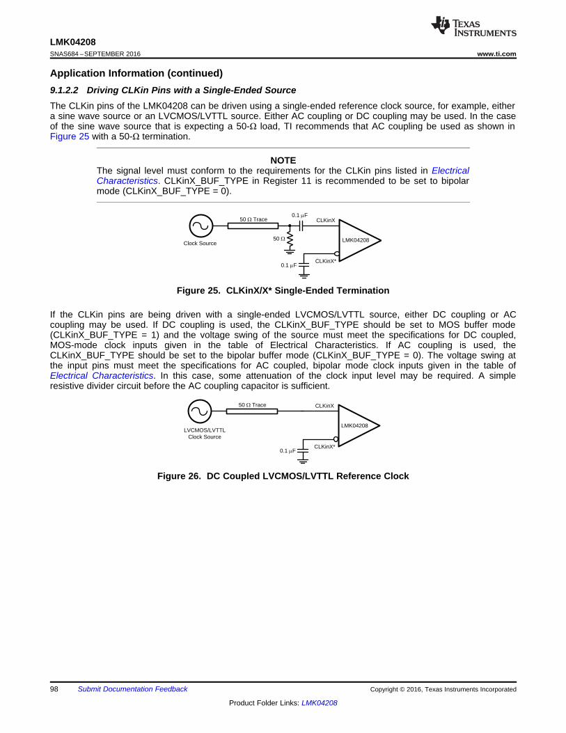
0.1 PF
50 :Trace
LMK04208LVCMOS/LVTTL
Clock Source
CLKinX
CLKinX*
0.1 PF
0.1 PF
50 :Trace
50 : LMK04208Clock Source
CLKinX
CLKinX*
98
LMK04208SNAS684 –SEPTEMBER 2016 www.ti.com
Product Folder Links: LMK04208
Submit Documentation Feedback Copyright © 2016, Texas Instruments Incorporated
Application Information (continued)9.1.2.2 Driving CLKin Pins with a Single-Ended SourceThe CLKin pins of the LMK04208 can be driven using a single-ended reference clock source, for example, eithera sine wave source or an LVCMOS/LVTTL source. Either AC coupling or DC coupling may be used. In the caseof the sine wave source that is expecting a 50-Ω load, TI recommends that AC coupling be used as shown inFigure 25 with a 50-Ω termination.
NOTEThe signal level must conform to the requirements for the CLKin pins listed in ElectricalCharacteristics. CLKinX_BUF_TYPE in Register 11 is recommended to be set to bipolarmode (CLKinX_BUF_TYPE = 0).
Figure 25. CLKinX/X* Single-Ended Termination
If the CLKin pins are being driven with a single-ended LVCMOS/LVTTL source, either DC coupling or ACcoupling may be used. If DC coupling is used, the CLKinX_BUF_TYPE should be set to MOS buffer mode(CLKinX_BUF_TYPE = 1) and the voltage swing of the source must meet the specifications for DC coupled,MOS-mode clock inputs given in the table of Electrical Characteristics. If AC coupling is used, theCLKinX_BUF_TYPE should be set to the bipolar buffer mode (CLKinX_BUF_TYPE = 0). The voltage swing atthe input pins must meet the specifications for AC coupled, bipolar mode clock inputs given in the table ofElectrical Characteristics. In this case, some attenuation of the clock input level may be required. A simpleresistive divider circuit before the AC coupling capacitor is sufficient.
Figure 26. DC Coupled LVCMOS/LVTTL Reference Clock
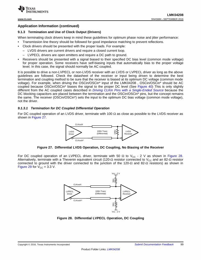
CLKoutX
CLKoutX*
LVPECL Receiver
50:
100:Trace(Differential)
50:
Vcc - 2 V
Vcc - 2 V
LVPECL Driver
CLKoutX
CLKoutX*
LVDS Receiver10
0:100:Trace(Differential)
LVDSDriver
99
LMK04208www.ti.com SNAS684 –SEPTEMBER 2016
Product Folder Links: LMK04208
Submit Documentation FeedbackCopyright © 2016, Texas Instruments Incorporated
Application Information (continued)9.1.3 Termination and Use of Clock Output (Drivers)When terminating clock drivers keep in mind these guidelines for optimum phase noise and jitter performance:• Transmission line theory should be followed for good impedance matching to prevent reflections.• Clock drivers should be presented with the proper loads. For example:
– LVDS drivers are current drivers and require a closed current loop.– LVPECL drivers are open emitters and require a DC path to ground.
• Receivers should be presented with a signal biased to their specified DC bias level (common mode voltage)for proper operation. Some receivers have self-biasing inputs that automatically bias to the proper voltagelevel. In this case, the signal should normally be AC coupled.
It is possible to drive a non-LVPECL or non-LVDS receiver with an LVDS or LVPECL driver as long as the aboveguidelines are followed. Check the datasheet of the receiver or input being driven to determine the besttermination and coupling method to be sure that the receiver is biased at its optimum DC voltage (common modevoltage). For example, when driving the OSCin/OSCin* input of the LMK04208 , OSCin/OSCin* should be ACcoupled because OSCin/OSCin* biases the signal to the proper DC level (See Figure 40) This is only slightlydifferent from the AC coupled cases described in Driving CLKin Pins with a Single-Ended Source because theDC blocking capacitors are placed between the termination and the OSCin/OSCin* pins, but the concept remainsthe same. The receiver (OSCin/OSCin*) sets the input to the optimum DC bias voltage (common mode voltage),not the driver.
9.1.3.1 Termination for DC Coupled Differential OperationFor DC coupled operation of an LVDS driver, terminate with 100 Ω as close as possible to the LVDS receiver asshown in Figure 27.
Figure 27. Differential LVDS Operation, DC Coupling, No Biasing of the Receiver
For DC coupled operation of an LVPECL driver, terminate with 50 Ω to VCC - 2 V as shown in Figure 28.Alternatively, terminate with a Thevenin equivalent circuit (120-Ω resistor connected to VCC and an 82-Ω resistorconnected to ground with the driver connected to the junction of the 120-Ω and 82-Ω resistors) as shown inFigure 29 for VCC = 3.3 V.
Figure 28. Differential LVPECL Operation, DC Coupling
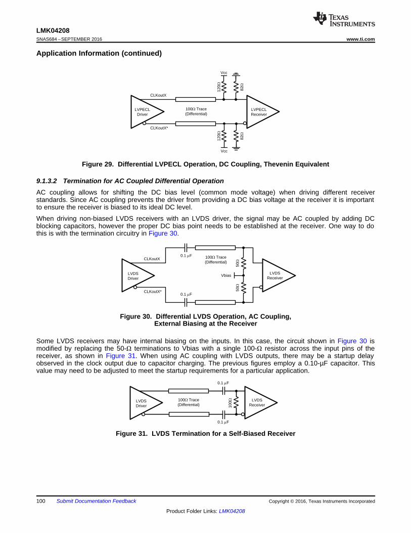
0.1 PF
0.1 PF
LVDSReceiver
100:Trace(Differential)
LVDSDriver 10
0:
CLKoutX
CLKoutX*
0.1 PF
0.1 PF
LVDS Receiver
50:
100:Trace(Differential)
LVDSDriver
50:
Vbias
CLKoutX
CLKoutX*
LVPECL Receiver
120:
100:Trace(Differential)
120:
Vcc
Vcc
LVPECL Driver
82:
82:
100
LMK04208SNAS684 –SEPTEMBER 2016 www.ti.com
Product Folder Links: LMK04208
Submit Documentation Feedback Copyright © 2016, Texas Instruments Incorporated
Application Information (continued)
Figure 29. Differential LVPECL Operation, DC Coupling, Thevenin Equivalent
9.1.3.2 Termination for AC Coupled Differential OperationAC coupling allows for shifting the DC bias level (common mode voltage) when driving different receiverstandards. Since AC coupling prevents the driver from providing a DC bias voltage at the receiver it is importantto ensure the receiver is biased to its ideal DC level.
When driving non-biased LVDS receivers with an LVDS driver, the signal may be AC coupled by adding DCblocking capacitors, however the proper DC bias point needs to be established at the receiver. One way to dothis is with the termination circuitry in Figure 30.
Figure 30. Differential LVDS Operation, AC Coupling,External Biasing at the Receiver
Some LVDS receivers may have internal biasing on the inputs. In this case, the circuit shown in Figure 30 ismodified by replacing the 50-Ω terminations to Vbias with a single 100-Ω resistor across the input pins of thereceiver, as shown in Figure 31. When using AC coupling with LVDS outputs, there may be a startup delayobserved in the clock output due to capacitor charging. The previous figures employ a 0.10-µF capacitor. Thisvalue may need to be adjusted to meet the startup requirements for a particular application.
Figure 31. LVDS Termination for a Self-Biased Receiver
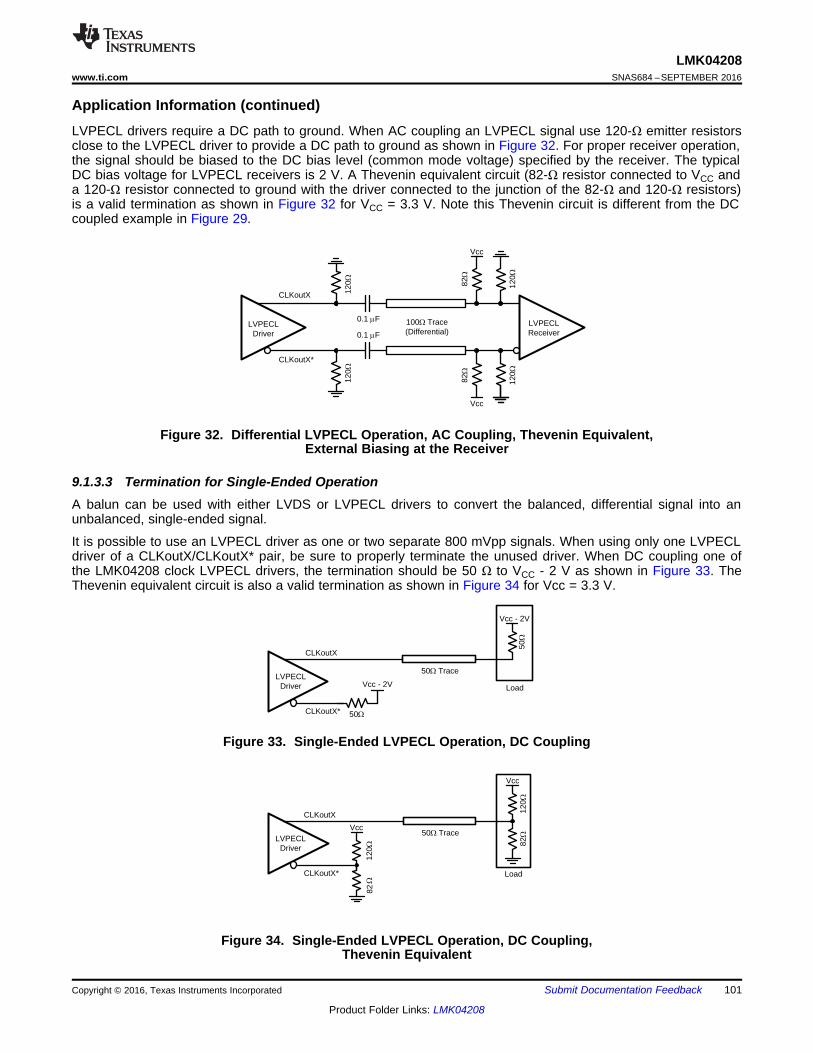
CLKoutX
CLKoutX*
:
50:Trace
120:
Load
Vcc
82:
120:
VccLVPECL
Driver
82
CLKoutX
CLKoutX* 50:
50:Trace
50:
Load
Vcc - 2V
Vcc - 2VLVPECL
Driver
CLKoutX
CLKoutX*
120:
120:
0.1 PF
0.1 PF
LVPECL Receiver
100:Trace(Differential)
LVPECLDriver
82:
120:
Vcc
82:
120:
Vcc
101
LMK04208www.ti.com SNAS684 –SEPTEMBER 2016
Product Folder Links: LMK04208
Submit Documentation FeedbackCopyright © 2016, Texas Instruments Incorporated
Application Information (continued)LVPECL drivers require a DC path to ground. When AC coupling an LVPECL signal use 120-Ω emitter resistorsclose to the LVPECL driver to provide a DC path to ground as shown in Figure 32. For proper receiver operation,the signal should be biased to the DC bias level (common mode voltage) specified by the receiver. The typicalDC bias voltage for LVPECL receivers is 2 V. A Thevenin equivalent circuit (82-Ω resistor connected to VCC anda 120-Ω resistor connected to ground with the driver connected to the junction of the 82-Ω and 120-Ω resistors)is a valid termination as shown in Figure 32 for VCC = 3.3 V. Note this Thevenin circuit is different from the DCcoupled example in Figure 29.
Figure 32. Differential LVPECL Operation, AC Coupling, Thevenin Equivalent,External Biasing at the Receiver
9.1.3.3 Termination for Single-Ended OperationA balun can be used with either LVDS or LVPECL drivers to convert the balanced, differential signal into anunbalanced, single-ended signal.
It is possible to use an LVPECL driver as one or two separate 800 mVpp signals. When using only one LVPECLdriver of a CLKoutX/CLKoutX* pair, be sure to properly terminate the unused driver. When DC coupling one ofthe LMK04208 clock LVPECL drivers, the termination should be 50 Ω to VCC - 2 V as shown in Figure 33. TheThevenin equivalent circuit is also a valid termination as shown in Figure 34 for Vcc = 3.3 V.
Figure 33. Single-Ended LVPECL Operation, DC Coupling
Figure 34. Single-Ended LVPECL Operation, DC Coupling,Thevenin Equivalent
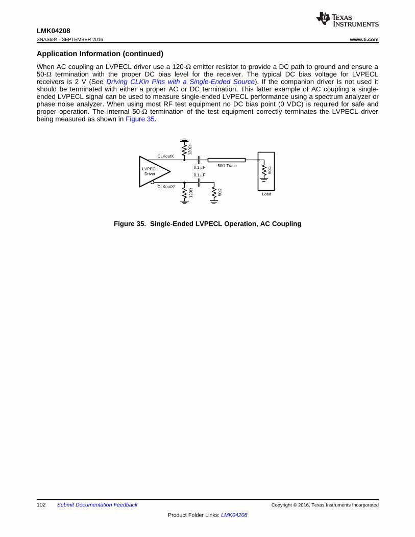
CLKoutX
CLKoutX*12
0:12
0:
0.1 PF
0.1 PF
50:Trace
50:
Load50:
LVPECLDriver
102
LMK04208SNAS684 –SEPTEMBER 2016 www.ti.com
Product Folder Links: LMK04208
Submit Documentation Feedback Copyright © 2016, Texas Instruments Incorporated
Application Information (continued)When AC coupling an LVPECL driver use a 120-Ω emitter resistor to provide a DC path to ground and ensure a50-Ω termination with the proper DC bias level for the receiver. The typical DC bias voltage for LVPECLreceivers is 2 V (See Driving CLKin Pins with a Single-Ended Source). If the companion driver is not used itshould be terminated with either a proper AC or DC termination. This latter example of AC coupling a single-ended LVPECL signal can be used to measure single-ended LVPECL performance using a spectrum analyzer orphase noise analyzer. When using most RF test equipment no DC bias point (0 VDC) is required for safe andproper operation. The internal 50-Ω termination of the test equipment correctly terminates the LVPECL driverbeing measured as shown in Figure 35.
Figure 35. Single-Ended LVPECL Operation, AC Coupling
103
LMK04208www.ti.com SNAS684 –SEPTEMBER 2016
Product Folder Links: LMK04208
Submit Documentation FeedbackCopyright © 2016, Texas Instruments Incorporated
Application Information (continued)9.1.4 Frequency Planning with the LMK04208Calculating the value of the output dividers for use with the LMK04208 is simple due to the architecture of theLMK04208. That is, the VCO divider may be bypassed and the clock output dividers allow for even and oddoutput divide values from 2 to 1045. For most applications, TI recommends bypassing the VCO divider.
The procedure for determining the needed LMK04208 device and clock output divider values for a set of clockoutput frequencies is straightforward.1. Calculate the least common multiple (LCM) of the clock output frequencies.2. Determine which VCO ranges will support the target clock output frequencies given the LCM.3. Determine the clock output divide values based on VCO frequency.4. Determine the PLL2_P, PLL2_N, and PLL2_R divider values given the OSCin VCXO or crystal frequency
and VCO frequency.
For example, given the following target output frequencies: 200 MHz, 120 MHz, and 25 MHz with a VCXOfrequency of 40 MHz:• First determine the LCM of the three frequencies. LCM(200 MHz, 120 MHz, 25 MHz) = 600 MHz. The LCM
frequency is the lowest frequency for which all of the target output frequencies are integer divisors of theLCM. Note: if there is one frequency which causes the LCM to be very large, greater than 3 GHz forexample, determine if there is a single frequency requirement which causes this. It may be possible to selectthe VCXO/crystal frequency to satisfy this frequency requirement through OSCout or CLKout3/4 driven byOSCin. In this way it is possible to get non-integer related frequencies at the outputs.
• Second, since the LCM is not in a VCO frequency range supported by the LMK04208, multiply the LCMfrequency by an integer which causes it to fall into a valid VCO frequency range of an LMK04208 device. Inthis case 600 MHz * 5 = 3000 MHz which is valid for the LMK04208.
• Third, continuing the example by using a VCO frequency of 3000 MHz and the LMK04208, the CLKoutdividers can be calculated by simply dividing the VCO frequency by the output frequency. To output 200 MHz,120 MHz, and 25 MHz the output dividers will be 12, 20, and 96 respectively.– 3000 MHz / 200 MHz = 15– 3000 MHz / 120 MHz = 25– 3000 MHz / 25 MHz = 120
• Fourth, PLL2 must be locked to its input reference. Refer to PLL Programming for more information on thistopic. By programming the clock output dividers and the PLL2 dividers the VCO can lock to the frequency of3000 MHz and the clock outputs dividers will each divide the VCO frequency down to the target outputfrequencies of 200 MHz, 120 MHz, and 25 MHz.
Refer to AN-1865, Frequency Synthesis and Planning for PLL Architectures for more information on this topicand LCM calculations.
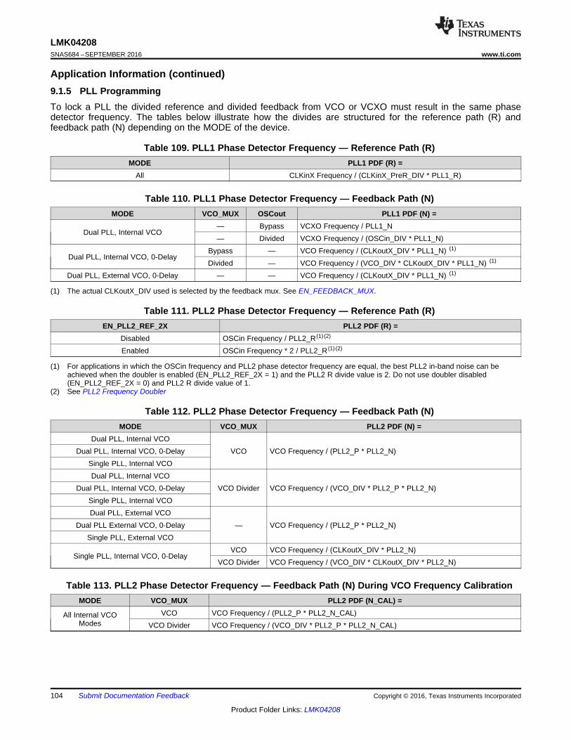
104
LMK04208SNAS684 –SEPTEMBER 2016 www.ti.com
Product Folder Links: LMK04208
Submit Documentation Feedback Copyright © 2016, Texas Instruments Incorporated
Application Information (continued)9.1.5 PLL ProgrammingTo lock a PLL the divided reference and divided feedback from VCO or VCXO must result in the same phasedetector frequency. The tables below illustrate how the divides are structured for the reference path (R) andfeedback path (N) depending on the MODE of the device.
Table 109. PLL1 Phase Detector Frequency — Reference Path (R)MODE PLL1 PDF (R) =
All CLKinX Frequency / (CLKinX_PreR_DIV * PLL1_R)
(1) The actual CLKoutX_DIV used is selected by the feedback mux. See EN_FEEDBACK_MUX.
Table 110. PLL1 Phase Detector Frequency — Feedback Path (N)MODE VCO_MUX OSCout PLL1 PDF (N) =
Dual PLL, Internal VCO— Bypass VCXO Frequency / PLL1_N— Divided VCXO Frequency / (OSCin_DIV * PLL1_N)
Dual PLL, Internal VCO, 0-DelayBypass — VCO Frequency / (CLKoutX_DIV * PLL1_N) (1)
Divided — VCO Frequency / (VCO_DIV * CLKoutX_DIV * PLL1_N) (1)
Dual PLL, External VCO, 0-Delay — — VCO Frequency / (CLKoutX_DIV * PLL1_N) (1)
(1) For applications in which the OSCin frequency and PLL2 phase detector frequency are equal, the best PLL2 in-band noise can beachieved when the doubler is enabled (EN_PLL2_REF_2X = 1) and the PLL2 R divide value is 2. Do not use doubler disabled(EN_PLL2_REF_2X = 0) and PLL2 R divide value of 1.
(2) See PLL2 Frequency Doubler
Table 111. PLL2 Phase Detector Frequency — Reference Path (R)EN_PLL2_REF_2X PLL2 PDF (R) =
Disabled OSCin Frequency / PLL2_R (1) (2)
Enabled OSCin Frequency * 2 / PLL2_R (1) (2)
Table 112. PLL2 Phase Detector Frequency — Feedback Path (N)MODE VCO_MUX PLL2 PDF (N) =
Dual PLL, Internal VCOVCO VCO Frequency / (PLL2_P * PLL2_N)Dual PLL, Internal VCO, 0-Delay
Single PLL, Internal VCODual PLL, Internal VCO
VCO Divider VCO Frequency / (VCO_DIV * PLL2_P * PLL2_N)Dual PLL, Internal VCO, 0-DelaySingle PLL, Internal VCODual PLL, External VCO
— VCO Frequency / (PLL2_P * PLL2_N)Dual PLL External VCO, 0-DelaySingle PLL, External VCO
Single PLL, Internal VCO, 0-DelayVCO VCO Frequency / (CLKoutX_DIV * PLL2_N)
VCO Divider VCO Frequency / (VCO_DIV * CLKoutX_DIV * PLL2_N)
Table 113. PLL2 Phase Detector Frequency — Feedback Path (N) During VCO Frequency CalibrationMODE VCO_MUX PLL2 PDF (N_CAL) =
All Internal VCOModes
VCO VCO Frequency / (PLL2_P * PLL2_N_CAL)VCO Divider VCO Frequency / (VCO_DIV * PLL2_P * PLL2_N_CAL)
2e6 × PLLX_WND_SIZE × fPDX
PLLX_DLD_CNTppm =
105
LMK04208www.ti.com SNAS684 –SEPTEMBER 2016
Product Folder Links: LMK04208
Submit Documentation FeedbackCopyright © 2016, Texas Instruments Incorporated
9.1.5.1 Example PLL2 N Divider ProgrammingTo program PLL2 to lock an LMK04208 using Dual PLL mode to a VCO frequency of 3000 MHz using a 40 MHzVCXO reference, first determine the total PLL2 N divide value. This is VCO Frequency / PLL2 phase detectorfrequency. This example assumes the PLL2 reference frequency doubler is enabled and a PLL2 R divide valueof 2 (see Note 1 in Table 111) which results in PLL2 phase detector frequency the same as PLL2 referencefrequency (40 MHz). 3000 MHz / 40 MHz = 75, so the total PLL2 N divide value is 75.
The dividers in the PLL2 N feedback path for Dual PLL mode include PLL2_P and PLL2_N. PLL2_P can beprogrammed from 2 to 8, including both even and odd values. PLL2_N can be programmed from 1 to 263,143,including both even and odd values. Since the total PLL2 N divide value of 75 contains the factors 3, 5, and 5, itwould be allowable to program PLL2_P to 3 or 5. It is simplest to use the smallest divide, so PLL2_P = 3, andPLL2_N = 25 which results in a Total PLL2 N = 75.
For this example and in most cases, PLL2_N_CAL will have the same value as PLL2_N. However when usingSingle PLL mode with 0-delay, the values will differ. When using an external VCO, PLL2_N_CAL value isunused.
9.1.6 Digital Lock Detect Frequency AccuracyThe digital lock detect circuit is used to determine PLL1 locked, PLL2 locked, and holdover exit events. A windowsize and lock count register are programmed to set a ppm frequency accuracy of reference to feedback signalsof the PLL for each event to occur. When a PLL digital lock event occurs the PLL's digital lock detect is assertedtrue. When the holdover exit event occurs, the device will exit holdover mode.
Table 114. Digital Lock Detect Frequency Accuracy TableEVENT PLL WINDOW SIZE LOCK COUNT
PLL1 Locked PLL1 PLL1_WND_SIZE PLL1_DLD_CNTPLL2 Locked PLL2 PLL2_WND_SIZE PLL2_DLD_CNTHoldover exit PLL1 PLL1_WND_SIZE HOLDOVER_DLD_CNT
For a digital lock detect event to occur there must be a “lock count” number of phase detector cycles of PLLXduring which the time/phase error of the PLLX_R reference and PLLX_N feedback signal edges are within theuser programmable "window size." Since there must be at least "lock count" phase detector events before a lockevent occurs, a minimum digital lock event time can be calculated as "lock count" / fPDX where X = 1 for PLL1 or2 for PLL2.
By using Equation 5, values for a "lock count" and "window size" can be chosen to set the frequency accuracyrequired by the system in ppm before the digital lock detect event occurs:
(5)
The effect of the "lock count" value is that it shortens the effective lock window size by dividing the "window size"by "lock count".
If at any time the PLLX_R reference and PLLX_N feedback signals are outside the time window set by "windowsize", then the “lock count” value is reset to 0.
9.1.6.1 Minimum Lock Time Calculation ExampleThe minimum time for PLL2 digital lock to be asserted can be calculated by Equation 6:
PLL2_DLD_CNT / Phase detector frequency (6)
Given a PLL2 phase detector frequency of 40 MHz and PLL2_DLD_CNT value of 10,000, the minimum digitallock detect time of PLL2 will be 10,000 / 40 MHz = 250 μs.
16¸¹
ᬩ
§¸¹
ᬩ
§»»
º««
ª0 digital delay =
CLKoutX_Y_DIVu CLKoutX_Y_DIV+ 0.5 - 11.5
106
LMK04208SNAS684 –SEPTEMBER 2016 www.ti.com
Product Folder Links: LMK04208
Submit Documentation Feedback Copyright © 2016, Texas Instruments Incorporated
9.1.7 Calculating Dynamic Digital Delay Values for Any DivideThis section explains how to calculate the dynamic digital delay for any divide value.
Dynamic digital delay allows the time offset between two or more clock outputs to be adjusted with no or minimalinterruption of clock outputs. Since the clock outputs are operating at a known frequency, the time offset can alsobe expressed as a phase shift. When dynamically adjusting the digital delay of clock outputs with differentfrequencies the phase shift should be expressed in terms of the higher frequency clock. The step size of thesmallest time adjustment possible is equal to half the period of the Clock Distribution Path, which is the VCOfrequency (Equation 3) or the VCO frequency divided by the VCO divider (Equation 4) if not bypassed. Thesmallest degree phase adjustment with respect to a clock frequency will be 360 * the smallest time adjustment *the clock frequency. The total number of phase offsets that the LMK04208 is able to achieve using dynamicdigital delay is equal 1 / (higher clock frequency * the smallest phase adjustment).
Equation 7 calculates the digital delay value that must be programmed for a synchronizing clock to achieve a 0time/phase offset from the qualifying clock. Once this digital delay value is known, it is possible to calculate thedigital delay value for any phase offset. The qualifying clock for dynamic digital delay is selected by theFEEDBACK_MUX. When dynamic digital delay is engaged with same clock output used for the qualifying clockand the new synchronized clock, it is termed relative dynamic digital delay since causing another SYNC eventwith the same digital delay value will offset the clock by the same phase once again. The important part ofrelative dynamic digital delay is that the CLKoutX_HS must be programmed correctly when the SYNC eventoccurs (Table 6). This can result in needing to program the device twice. Once to set the new CLKoutX_DDLYwith CLKoutX_HS as required for the SYNC event, and again to set the CLKoutX_HS to its desired value.
Digital delay values are programmed using the CLKoutX_DDLY and CLKoutX_HS registers as shown inEquation 8. For example, to achieve a digital delay of 13.5, program CLKoutX_DDLY = 14 and CLKoutX_HS = 1.
(7)
Equation 7 uses the ceiling operator. To find the ceiling of a fractional number round up. An integer remains thesame value.Digital delay = CLKoutX_DDLY - (0.5 * CLKoutX_HS) (8)
Note: since the digital delay value for 0 time/phase offset is a function of the qualifying clock's divide value, theresulting digital delay value can be used for any clock output operating at any frequency to achieve a 0time/phase offset from the qualifying clock. Therefore the calculated time shift table will also be the same as inTable 115.
9.1.7.1 ExampleConsider a system with:• A VCO frequency of 3000 MHz.• The VCO divider is bypassed, therefore the clock distribution path frequency is 3000 MHz.• CLKout0_DIV = 10 resulting in a 300 MHz frequency on CLKout0.• CLKout1_DIV = 20 resulting in a 150 MHz frequency on CLKout2.
For this system the minimum time adjustment is ~0.16667 ns, which is 0.5 / (3000 MHz). Since the higherfrequency is 300 MHz, phase adjustments will be calculated with respect to the 300 MHz frequency. The 0.25 nsminimum time adjustment results in a minimum phase adjustment of 18 degrees, which is 360 degrees / 200MHz * 0.25 ns.
To calculate the digital delay value to achieve a 0 time/phase shift of CLKout2 when CLKout0 is the qualifyingclock. Solve Equation 7 using the divide value of 10. To solve the equation 16/10 = 1.6, the ceiling of 1.6 is 2.Then to finish solving the equation solve (2 + 0.5) * 10 - 11.5 = 13.5. A digital delay value of 13.5 is programmedby setting CLKout1_DDLY = 14 and CLKout1_HS = 1.
To calculate the digital delay value to achieve a 0 time/phase shift of CLKout0 when CLKout2 is the qualifyingclock, solve Equation 7 using the divide value of CLKout2, which is 20. This results in a digital delay of 18.5which is programmed as CLKout0_DDLY = 19 and CLKout0_HS = 1.
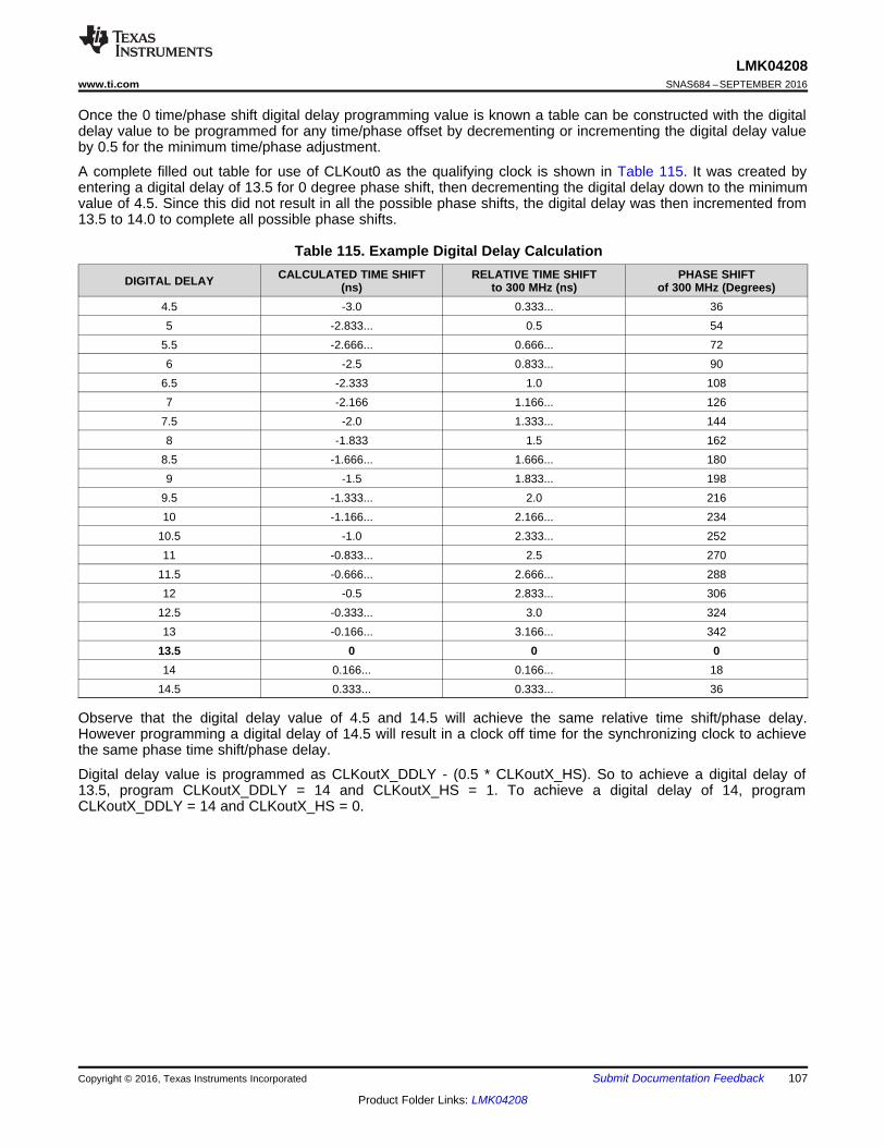
107
LMK04208www.ti.com SNAS684 –SEPTEMBER 2016
Product Folder Links: LMK04208
Submit Documentation FeedbackCopyright © 2016, Texas Instruments Incorporated
Once the 0 time/phase shift digital delay programming value is known a table can be constructed with the digitaldelay value to be programmed for any time/phase offset by decrementing or incrementing the digital delay valueby 0.5 for the minimum time/phase adjustment.
A complete filled out table for use of CLKout0 as the qualifying clock is shown in Table 115. It was created byentering a digital delay of 13.5 for 0 degree phase shift, then decrementing the digital delay down to the minimumvalue of 4.5. Since this did not result in all the possible phase shifts, the digital delay was then incremented from13.5 to 14.0 to complete all possible phase shifts.
Table 115. Example Digital Delay Calculation
DIGITAL DELAY CALCULATED TIME SHIFT(ns)
RELATIVE TIME SHIFTto 300 MHz (ns)
PHASE SHIFTof 300 MHz (Degrees)
4.5 -3.0 0.333... 365 -2.833... 0.5 54
5.5 -2.666... 0.666... 726 -2.5 0.833... 90
6.5 -2.333 1.0 1087 -2.166 1.166... 126
7.5 -2.0 1.333... 1448 -1.833 1.5 162
8.5 -1.666... 1.666... 1809 -1.5 1.833... 198
9.5 -1.333... 2.0 21610 -1.166... 2.166... 234
10.5 -1.0 2.333... 25211 -0.833... 2.5 270
11.5 -0.666... 2.666... 28812 -0.5 2.833... 306
12.5 -0.333... 3.0 32413 -0.166... 3.166... 342
13.5 0 0 014 0.166... 0.166... 18
14.5 0.333... 0.333... 36
Observe that the digital delay value of 4.5 and 14.5 will achieve the same relative time shift/phase delay.However programming a digital delay of 14.5 will result in a clock off time for the synchronizing clock to achievethe same phase time shift/phase delay.
Digital delay value is programmed as CLKoutX_DDLY - (0.5 * CLKoutX_HS). So to achieve a digital delay of13.5, program CLKoutX_DDLY = 14 and CLKoutX_HS = 1. To achieve a digital delay of 14, programCLKoutX_DDLY = 14 and CLKoutX_HS = 0.
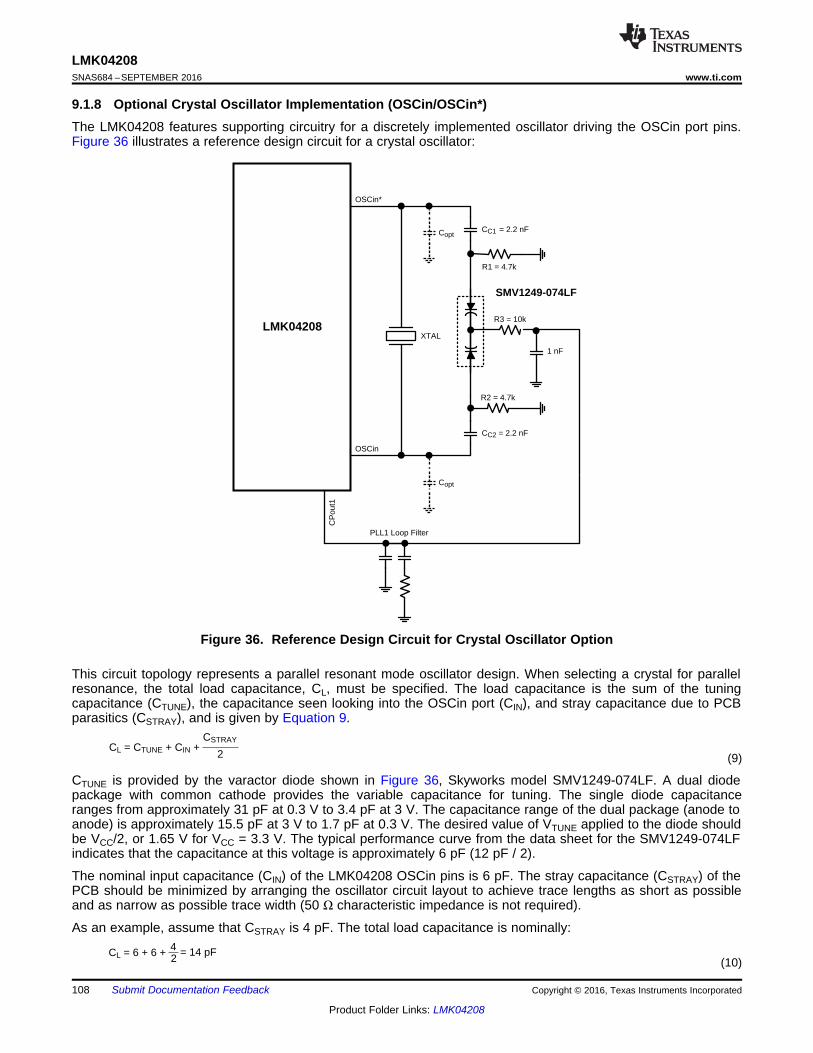
2CL = 6 + 6 + 4 = 14 pF
2
CSTRAYCL = CTUNE + CIN +
CP
out1
LMK04208
OSCin
OSCin*
PLL1 Loop Filter
XTAL
CC1 = 2.2 nF
CC2 = 2.2 nF
R1 = 4.7k
R3 = 10k
1 nF
R2 = 4.7k
SMV1249-074LF
Copt
Copt
108
LMK04208SNAS684 –SEPTEMBER 2016 www.ti.com
Product Folder Links: LMK04208
Submit Documentation Feedback Copyright © 2016, Texas Instruments Incorporated
9.1.8 Optional Crystal Oscillator Implementation (OSCin/OSCin*)The LMK04208 features supporting circuitry for a discretely implemented oscillator driving the OSCin port pins.Figure 36 illustrates a reference design circuit for a crystal oscillator:
Figure 36. Reference Design Circuit for Crystal Oscillator Option
This circuit topology represents a parallel resonant mode oscillator design. When selecting a crystal for parallelresonance, the total load capacitance, CL, must be specified. The load capacitance is the sum of the tuningcapacitance (CTUNE), the capacitance seen looking into the OSCin port (CIN), and stray capacitance due to PCBparasitics (CSTRAY), and is given by Equation 9.
(9)
CTUNE is provided by the varactor diode shown in Figure 36, Skyworks model SMV1249-074LF. A dual diodepackage with common cathode provides the variable capacitance for tuning. The single diode capacitanceranges from approximately 31 pF at 0.3 V to 3.4 pF at 3 V. The capacitance range of the dual package (anode toanode) is approximately 15.5 pF at 3 V to 1.7 pF at 0.3 V. The desired value of VTUNE applied to the diode shouldbe VCC/2, or 1.65 V for VCC = 3.3 V. The typical performance curve from the data sheet for the SMV1249-074LFindicates that the capacitance at this voltage is approximately 6 pF (12 pF / 2).
The nominal input capacitance (CIN) of the LMK04208 OSCin pins is 6 pF. The stray capacitance (CSTRAY) of thePCB should be minimized by arranging the oscillator circuit layout to achieve trace lengths as short as possibleand as narrow as possible trace width (50 Ω characteristic impedance is not required).
As an example, assume that CSTRAY is 4 pF. The total load capacitance is nominally:
(10)
1(C0 + CL1)
- 1(C0 + CL2)
=21À
FFCL1
FCL1 - FCL2=
2À
C1=F
'F C0
C1¸¹
ᬩ
§ CL2
C1+
1-C0
C1¸¹
ᬩ
§ CL1
C1+
1
2(C0 + CL1)+ 1 C0
C1¸¹
ᬩ
§ CL
C1+
1+ 1
2
C1FL = FS À = FS À
109
LMK04208www.ti.com SNAS684 –SEPTEMBER 2016
Product Folder Links: LMK04208
Submit Documentation FeedbackCopyright © 2016, Texas Instruments Incorporated
(1) Performance data and crystal specifications contained in this section are based on Vectron model VXB1-1150-20M480, 20.48 MHz.PLL1 has a narrow loop bandwidth, PLL2 loop parameters are: C1 = 150 pF, C2 = 120 nF, R2 = 470 Ω, Charge Pump current = 3.2 mA,Phase detector frequency = 20.48 MHz or 40.96 MHz, VCO frequency = 2949.12 MHz. Loop filter was optimized for 40.96 MHz phasedetector performance.
Consequently the load capacitance specification for the crystal in this case should be nominally 14 pF.
The 2.2-nF capacitors shown in the circuit are coupling capacitors that block the DC tuning voltage applied bythe 4.7-kΩ and 10-kΩ resistors. The value of these coupling capacitors should be large, relative to the value ofCTUNE (CC1 = CC2 >> CTUNE), so that CTUNE becomes the dominant capacitance.
For a specific value of CL, the corresponding resonant frequency (FL) of the parallel resonant mode circuit is:
where• FS = Series resonant frequency• C1 = Motional capacitance of the crystal• CL = Load capacitance• C0 = Shunt capacitance of the crystal, specified on the crystal datasheet (11)
The normalized tuning range of the circuit is closely approximated by:
(12)
CL1, CL2 = The endpoints of the circuit’s load capacitance range, assuming a variable capacitance element is onecomponent of the load. FCL1, FCL2 = parallel resonant frequencies at the extremes of the circuit’s loadcapacitance range.
A common range for the pullability ratio, C0/C1, is 250 to 280. The ratio of the load capacitance to the shuntcapacitance is ~(n * 1000), n < 10. Hence, picking a crystal with a smaller pullability ratio supports a wider tuningrange because this allows the scale factors related to the load capacitance to dominate.
9.1.8.1 Examples of Phase Noise and Jitter PerformanceExamples of the phase noise and jitter performance of the LMK04208 with a crystal oscillator are shown inTable 116. This table illustrates the clock output phase noise when a 20.48-MHz crystal is paired with PLL1.Performance of other LMK04208 devices will be similar.
Table 116. Example RMS Jitter and Clock Output Phase Noise for LMK04208with a 20.48 MHz Crystal Driving OSCin (T = 25 °C, VCC = 3.3 V) (1)
INTEGRATIONBANDWIDTH CLOCK OUTPUT TYPE
PLL2 PDF = 20.48 MHz(EN_PLL2_REF2X = 0,
XTAL_LVL = 3)PLL2 PDF = 40.96 MHz
(EN_PLL2_REF2X = 1, XTAL_LVL = 3)
fCLK = 245.76 MHz fCLK = 122.88 MHz fCLK = 245.76 MHzRMS JITTER (fs, RMS)
100 Hz – 20 MHzLVCMOS 374 412 382
LVDS 419 421 372LVPECL 1.6 Vpp 460 448 440
10 kHz – 20 MHzLVCMOS 226 195 190
LVDS 231 205 194LVPECL 1.6 Vpp 226 191 188
110
LMK04208SNAS684 –SEPTEMBER 2016 www.ti.com
Product Folder Links: LMK04208
Submit Documentation Feedback Copyright © 2016, Texas Instruments Incorporated
Table 116. Example RMS Jitter and Clock Output Phase Noise for LMK04208with a 20.48 MHz Crystal Driving OSCin (T = 25 °C, VCC = 3.3 V) (1) (continued)
INTEGRATIONBANDWIDTH CLOCK OUTPUT TYPE
PLL2 PDF = 20.48 MHz(EN_PLL2_REF2X = 0,
XTAL_LVL = 3)PLL2 PDF = 40.96 MHz
(EN_PLL2_REF2X = 1, XTAL_LVL = 3)
fCLK = 245.76 MHz fCLK = 122.88 MHz fCLK = 245.76 MHzPHASE NOISE (dBc/Hz)
Offset Clock Output Type
PLL2 PDF = 20.48 MHz(EN_PLL2_REF2X = 0,
XTAL_LVL = 3)
PLL2 PDF = 40.96 MHz(EN_PLL2_REF2X = 1, XTAL_LVL = 3)
fCLK = 245.76 MHz fCLK = 122.88 MHz fCLK = 245.76 MHz
100 HzLVCMOS -87 -93 -87
LVDS -86 -91 -86LVPECL 1.6 Vpp -86 -92 -85
1 kHzLVCMOS -115 -121 -115
LVDS -115 -123 -116LVPECL 1.6 Vpp -114 -122 -116
10 kHzLVCMOS -117 -128 -122
LVDS -117 -128 -122LVPECL 1.6 Vpp -117 -128 -122
100 kHzLVCMOS -130 -135 -129
LVDS -130 -135 -129LVPECL 1.6 Vpp -129 -135 -129
1 MHzLVCMOS -150 -154 -148
LVDS -149 -153 -148LVPECL 1.6 Vpp -150 -154 -148
40 MHzLVCMOS -159 -162 -159
LVDS -157 -159 -157LVPECL 1.6 Vpp -159 -161 -159
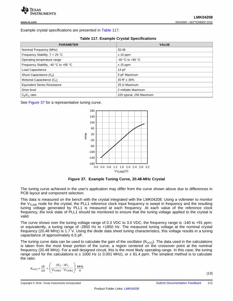
KVCO ='F'V
,MHz
V= ¸
¹
ᬩ
§ 'F2 - 'F1
VTUNE2 - VTUNE1
0.0 0.4 0.8 1.2 1.6 2.0 2.4 2.8 3.2-180
-140
-100
-60
-20
20
60
100
140
180
PP
M
VTUNE(V)
111
LMK04208www.ti.com SNAS684 –SEPTEMBER 2016
Product Folder Links: LMK04208
Submit Documentation FeedbackCopyright © 2016, Texas Instruments Incorporated
Example crystal specifications are presented in Table 117.
Table 117. Example Crystal SpecificationsPARAMETER VALUE
Nominal Frequency (MHz) 20.48Frequency Stability, T = 25 °C ± 10 ppmOperating temperature range -40 °C to +85 °CFrequency Stability, -40 °C to +85 °C ± 15 ppmLoad Capacitance 14 pFShunt Capacitance (C0) 5 pF MaximumMotional Capacitance (C1) 20 fF ± 30%Equivalent Series Resistance 25 Ω MaximumDrive level 2 mWatts MaximumC0/C1 ratio 225 typical, 250 Maximum
See Figure 37 for a representative tuning curve.
Figure 37. Example Tuning Curve, 20.48-MHz Crystal
The tuning curve achieved in the user's application may differ from the curve shown above due to differences inPCB layout and component selection.
This data is measured on the bench with the crystal integrated with the LMK04208. Using a voltmeter to monitorthe VTUNE node for the crystal, the PLL1 reference clock input frequency is swept in frequency and the resultingtuning voltage generated by PLL1 is measured at each frequency. At each value of the reference clockfrequency, the lock state of PLL1 should be monitored to ensure that the tuning voltage applied to the crystal isvalid.
The curve shows over the tuning voltage range of 0.3 VDC to 3.0 VDC, the frequency range is -140 to +91 ppm;or equivalently, a tuning range of -2850 Hz to +1850 Hz. The measured tuning voltage at the nominal crystalfrequency (20.48 MHz) is 1.7 V. Using the diode data sheet tuning characteristics, this voltage results in a tuningcapacitance of approximately 6.5 pF.
The tuning curve data can be used to calculate the gain of the oscillator (KVCO). The data used in the calculationsis taken from the most linear portion of the curve, a region centered on the crossover point at the nominalfrequency (20.48 MHz). For a well designed circuit, this is the most likely operating range. In this case, the tuningrange used for the calculations is ± 1000 Hz (± 0.001 MHz), or ± 81.4 ppm. The simplest method is to calculatethe ratio:
(13)
= 0.00164,MHz
V(2.03 - 0.814) À 106
12.288 À 81.4 - (-81.4)( )
'V À 106
FNOM À ('ppm2 - 'ppm1)KVCO =
= 0.00164MHz
V2.03 - 0.8140.001 - (-0.001)
112
LMK04208SNAS684 –SEPTEMBER 2016 www.ti.com
Product Folder Links: LMK04208
Submit Documentation Feedback Copyright © 2016, Texas Instruments Incorporated
ΔF2 and ΔF1 are in units of MHz. Using data from the curve this becomes:
(14)
A second method uses the tuning data in units of ppm:
(15)
FNOM is the nominal frequency of the crystal and is in units of MHz. Using the data, this becomes:
(16)
In order to ensure startup of the oscillator circuit, the equivalent series resistance (ESR) of the selected crystalshould conform to the specifications listed in the table of Electrical Characteristics.
It is also important to select a crystal with adequate power dissipation capability, or drive level. If the drive levelsupplied by the oscillator exceeds the maximum specified by the crystal manufacturer, the crystal will undergoexcessive aging and possibly become damaged. Drive level is directly proportional to resonant frequency,capacitive load seen by the crystal, voltage and equivalent series resistance (ESR).
For more complete coverage of crystal oscillator design, see:
Clocks and Timers or AN-1939 Crystal Based Oscillator Design with the LMK04000 Family.
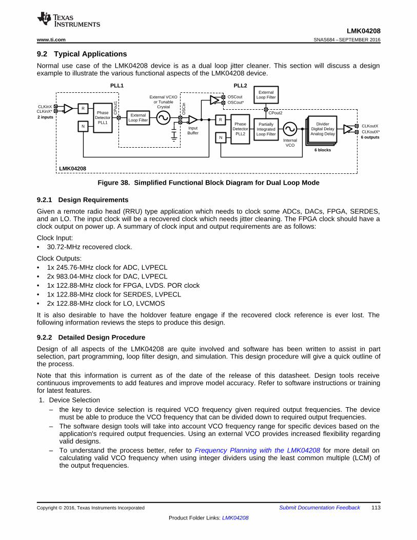
RCLKinXCLKinX*
N
Phase Detector
PLL1
External VCXO or Tunable
Crystal
R
N
Phase Detector
PLL2
InternalVCO
ExternalLoop Filter
OS
Cin
CP
out1
OSCoutOSCout*
LMK04208
CPout2
Partially Integrated Loop Filter
6 outputs
External Loop Filter
PLL1 PLL2
6 blocks
2 inputs
Input Buffer
CLKoutXCLKoutX*
Divider
Digital DelayAnalog Delay
113
LMK04208www.ti.com SNAS684 –SEPTEMBER 2016
Product Folder Links: LMK04208
Submit Documentation FeedbackCopyright © 2016, Texas Instruments Incorporated
9.2 Typical ApplicationsNormal use case of the LMK04208 device is as a dual loop jitter cleaner. This section will discuss a designexample to illustrate the various functional aspects of the LMK04208 device.
Figure 38. Simplified Functional Block Diagram for Dual Loop Mode
9.2.1 Design RequirementsGiven a remote radio head (RRU) type application which needs to clock some ADCs, DACs, FPGA, SERDES,and an LO. The input clock will be a recovered clock which needs jitter cleaning. The FPGA clock should have aclock output on power up. A summary of clock input and output requirements are as follows:
Clock Input:• 30.72-MHz recovered clock.
Clock Outputs:• 1x 245.76-MHz clock for ADC, LVPECL• 2x 983.04-MHz clock for DAC, LVPECL• 1x 122.88-MHz clock for FPGA, LVDS. POR clock• 1x 122.88-MHz clock for SERDES, LVPECL• 2x 122.88-MHz clock for LO, LVCMOS
It is also desirable to have the holdover feature engage if the recovered clock reference is ever lost. Thefollowing information reviews the steps to produce this design.
9.2.2 Detailed Design ProcedureDesign of all aspects of the LMK04208 are quite involved and software has been written to assist in partselection, part programming, loop filter design, and simulation. This design procedure will give a quick outline ofthe process.
Note that this information is current as of the date of the release of this datasheet. Design tools receivecontinuous improvements to add features and improve model accuracy. Refer to software instructions or trainingfor latest features.1. Device Selection
– the key to device selection is required VCO frequency given required output frequencies. The devicemust be able to produce the VCO frequency that can be divided down to required output frequencies.
– The software design tools will take into account VCO frequency range for specific devices based on theapplication's required output frequencies. Using an external VCO provides increased flexibility regardingvalid designs.
– To understand the process better, refer to Frequency Planning with the LMK04208 for more detail oncalculating valid VCO frequency when using integer dividers using the least common multiple (LCM) ofthe output frequencies.
114
LMK04208SNAS684 –SEPTEMBER 2016 www.ti.com
Product Folder Links: LMK04208
Submit Documentation Feedback Copyright © 2016, Texas Instruments Incorporated
Typical Applications (continued)2. Device Configuration
– There are many possible permutations of dividers and other registers to get same input and outputfrequencies from a device. However there are some optimizations and trade-offs to be considered.– If more than one divider is in series, for instance VCO divider to CLKout divider, or VCO divider to PLL
prescaler to PLL N. It is possible although not assured that some crosstalk/mixing could be createdwhen using some divides.
– The design software normally attempts to maximize phase detector frequency, use smallest dividers, andmaximizes PLL charge pump current.
– When an external VCXO or crystal is used for jitter cleaning, the design software will choose themaximum frequency value, depending on design software options, this max frequency may be limited tostandard value VCXOs/Crystals. Note, depending on application, different frequency VCXOs may bechosen to generate some of the required output frequencies.
– Refer to PLL Programming for divider equations need to ensure PLL is locked. The design software isable to configure the device for most cases, but at this time for advanced features like 0-delay, theuser must take care to ensure proper PLL programming.
– These guidelines may be followed when configuring PLL related dividers or other related registers:– For lowest possible in-band PLL flat noise, maximize phase detector frequency to minimize N divide
value.– For lowest possible in-band PLL flat noise, maximize charge pump current. The highest value charge
pump currents often have similar performance due to diminishing returns.– To reduce loop filter component sizes, increase N value and/or reduce charge pump current.– Large capacitors help reduce phase detector spurs at phase detector frequency caused by external
VCOs/VCXOs with low input impedance.– As rule of thumb, keeping the phase detector frequency approximately between 10 * PLL loop
bandwidth and 100 * PLL loop bandwidth. A phase detector frequency less than 5 * PLL bandwidthmay be unstable and a phase detector frequency > 100 * loop bandwidth may experience increasedlock time due to cycle slipping. However for clock generation/jitter cleaning applications, lock time istypically not critical and large phase detector frequencies typically result in reduced PLL noise, socycle-slipping during lock is acceptable.
3. PLL Loop Filter Design– TI recommends using Clock Architect to design your loop filter.– Best loop filter design and simulation can be achieved when:
– Custom reference and VCXO phase noise profiles are loaded into the software.– VCO gain of the external VCXO or possible external VCO device are entered.
– The design tool will return solutions with high reference/phase detector frequencies and high chargepump currents by default. It is possible to reduce the phase detector frequency charge pump current inClock Architect. Due to the narrow loop bandwidth used on PLL1, it is common to lower the phasedetector frequency and/or charge pump current on PLL1 to reduce component size.
– While designing loop filter, adjusting the charge pump current or N value can help with loop filtercomponent selection. Lower charge pump currents and larger N values result in smaller componentvalues but may increase impacts of leakage and reduce PLL phase noise performance.
– More detailed understanding of loop filter design can found in Dean Banerjee's PLL Performance,Simulation, and Design (www.ti.com/tool/pll_book).
115
LMK04208www.ti.com SNAS684 –SEPTEMBER 2016
Product Folder Links: LMK04208
Submit Documentation FeedbackCopyright © 2016, Texas Instruments Incorporated
Typical Applications (continued)4. Clock Output Assignment
– At this time the design software does not take into account frequency assignment to specific outputsexcept to ensure that the output frequencies can be achieved. It is best to consider proximity of eachclock output to each other and other PLL circuitry when choosing final clock output locations. Here aresome guidelines to help achieve best performance when assigning outputs to specific CLKout/OSCoutpins.– Group common frequencies together.– PLL charge pump circuitry can cause crosstalk at charge pump frequency. Place outputs sharing
charge pump frequency or lower priority outputs not sensitive to charge pump frequency spurstogether.
– Muxes can create a path for noise coupling. Consider all frequencies which may have some bleedthrough from non-selected mux inputs.– For example, LMK04208 CLKout3 and CLKout4 share a mux with OSCin.
– Some clock targets require low close-in phase noise. If possible, use a VCXO based PLL1 output fromCLKout3 or CLKout4 for such a clock target. An example is a clock to a PLL reference.
– Some clock targets require excellent noise floor performance. Outputs driven by the internal VCO havethe best noise floor performance. An example is an ADC or DAC.
5. Other device specific configuration. For LMK04208, consider the following:– PLL lock time based on programming:
– In addition to the time it takes the device to lock to frequency, there is a digital filter to avoid false locktime detects which can also be used to ensure a specific PPM frequency accuracy. This also impactsthe time it takes for the digital lock detect (DLD) pin to be asserted. Refer to Digital Lock DetectFrequency Accuracy for more information.
– Holdover configuration:– Specific PPM frequency accuracy required to exit holdover can be programmed. Refer to Digital Lock
Detect Frequency Accuracy for more information.– Digital delay: phase alignment of the output clocks.– Analog delay: another method to shift phases of clocks with finer resolution with the penalty of increase
noise floor.– Dynamic digital delay: ability to shift phase alignment of clocks with minimum disruption during operation.
6. Device Programming– The software tool TICS Pro for EVM programming can be used to setup the device in the desired
configuration, then export a hex register map suitable for use in application.
Some additional information on each part of the design procedure for the RRU example is below.
9.2.2.1 Device SelectionUse the WEBENCH Clock Architect Tool. Enter the required frequencies and formats into the tool. To use thisdevice, find a solution using the LMK04208.
9.2.2.1.1 Clock Architect
When viewing resulting solutions, it is possible to narrow the parts used in the solution by setting a filter.
Filtering of a specific device can be done by selecting the device from the filter combo box. Also, regularexpressions can be typed into filter combo box. LMK04208 will filter for only the LMK04208 device.
To simulate single loop solutions with dual loop device, set PLL1 loop filter to a very narrow or "0 Hz LBW."
9.2.2.1.2 Calculation Using LCM
In this example, the LCM(245.76 MHz, 983.04 MHz, 122.88 MHz) = 983.04 MHz. A valid VCO frequency forLMK04208 is 2949.12 MHz = 3 * 983.04 MHz. Therefore the LMK04208 may be used to produce these outputfrequencies.
116
LMK04208SNAS684 –SEPTEMBER 2016 www.ti.com
Product Folder Links: LMK04208
Submit Documentation Feedback Copyright © 2016, Texas Instruments Incorporated
Typical Applications (continued)9.2.2.2 Device ConfigurationThe tools automatically configure the simulation to meet the input and output frequency requirements given andmake assumptions about other parameters to give some default simulations. The assumptions made are tomaximize input frequencies, phase detector frequencies, and charge pump currents while minimizing VCOfrequency and divider values.
9.2.2.2.1 PLL LO Reference
PLL1 outputs have the best phase noise performance for LO references. As such OSCout, or CLKout3/CLKout4(with CLKout#_OSCin_Sel field selecting OSCin clock source) can be used to provide the 122.88 MHz LOreference clock. To achieve this with a 245.76 MHz VCXO the OSCout_DIV can be set to 2 to provide 122.88MHz at OSCout. CLKout3/4_DIV can be set to 2 for 122.88 MHz output if LO references are clocked fromCLKout3/4.
In the next section it is determined that for the POR clock, a 122.88 MHz VCXO will be used. This means nodivision will be needed to provide 122.88 MHz.
117
LMK04208www.ti.com SNAS684 –SEPTEMBER 2016
Product Folder Links: LMK04208
Submit Documentation FeedbackCopyright © 2016, Texas Instruments Incorporated
Typical Applications (continued)9.2.2.2.2 POR Clock
If OSCout is to be used for LVDS POR 122.88 MHz clock, the POR value of the OSCout_DIV is 1, so a 122.88MHz VCXO frequency must be chosen. This may be desired anyway since the phase detector frequency islimited to 122.88 MHz and lower frequency VCXOs tend to cost less. With this change the OSCin frequency andphase detector frequency are the same, so the doubler must be enabled and the PLL2 R divider programmed =2 to follow the rule stated in PLL2 Frequency Doubler.
Note: it is possible to set the PLL2 R = 0.5 to simulate the doubler in-case lower frequency VCXOs would like tobe simulated. For example a 61.44 MHz VCXO could be used while retaining a 122.88 MHz phase detectorfrequency. However, it would reduce the LO reference frequency and POR clock frequency to 61.44 MHz.
At this time, the VCXO frequency and phase detector frequency is chosen, so loop filter design may begin.
9.2.2.3 PLL Loop Filter DesignThe PLL structure for the LMK04208 is illustrated in Loop Filter.
At this time the user may choose to make adjustments to the simulation tools for more accurate simulations totheir application. For example:• Clock Architect allows loading a custom phase noise plot for any block. Typically, a custom phase noise plot
is entered for CLKin to match the reference phase noise to the device; a phase noise plot for the VCXO canadditionally be provided to match the performance of VCXO used. For improved accuracy in simulation andoptimum loop filter design, be sure to load these custom noise profiles for use in application. After loading aphase noise plot, user should recalculate the recommended loop filter design.
• The Clock Architect will return solutions with high reference/phase detector frequencies by default. The usermay decrease the phase detector frequency if desired. Be sure to decrease by integer relationships with thereference as an integer divider will be used. Due to the narrow loop bandwidth used on PLL1, it is common toreduce the phase detector frequency on PLL1 by increasing PLL1 R.
For this example, for PLL1 to perform jitter cleaning and to minimize jitter from PLL2 used for frequencymultiplication:• PLL1: A narrow loop bandwidth PLL1 filter was design by updating the loop bandwidth to 50 Hz and phase
margin to 50 degrees.• PLL2:
– VCXO noise profile is measured, then loaded into VCXO phase noise profile in Clock Architect. Be surethat the VCO frequency of PLL1 is as desired. If changing the VC(X)O frequency of PLL1, be sure to thePLL2 Phase Detector frequency aligns with an integer divider.
– The recommended loop filter is redesigned. Updates to the PLL1 loop filter and VCXO phase noise maychange the loop filter recommendation, so PLL2 loop filter may need to be recalculated.
The next two sections will discuss PLL1 and PLL2 loop filter design specific to this example using default phasenoise profiles.
NOTEClock Architect provides some recommend loop filters upon first load of the simulation.Anytime PLL related inputs change like an input phase noise, charge pump current,divider values, and so forth. it is best to re-design the PLL1 loop filter to the recommendeddesign or your desired parameters. After PLL1, then update the PLL2 loop filter in thesame way to keep the loop filters designed and optimized for the application. Since PLL1loop filter design may impact PLL2 loop filter design, be sure to update the designs inorder.
118
LMK04208SNAS684 –SEPTEMBER 2016 www.ti.com
Product Folder Links: LMK04208
Submit Documentation Feedback Copyright © 2016, Texas Instruments Incorporated
Typical Applications (continued)9.2.2.3.1 PLL1 Loop Filter Design
For this example, in the Clock Architect tool update the loop bandwidth for 0.05 kHz and the phase margin for 50degrees and press "Choose RC Components for me." With the 30.72 MHz phase detector frequency and 1.6 mAcharge pump; the designed loop filter's largest capacitor, C2, is 27 µF. Supposing a goal of < 10 µF; setting PLL1R = 4 and pressing the calculate again shows that C2 is 6.8 µF. Suppose that a reduction to < 1 µF is desired,continuing to increase the PLL1 R to 8 resulting in a phase detector frequency of 3.84 MHz and reducing thecharge pump current from 1.6 mA to 0.4 mA and calculating again shows that C2 is 820 nF. As N was increasedand charge pump decreased, this final design has R2 = 12 kΩ. The first design with low N value and high chargepump current result in R2 = 390 Ω. The impact of the thermal resistance is calculated in the tool. Viewing thesimulation of the loop filter with the 12-kΩ resistor shows that the thermal noise in the loop is not impactingperformance.
It may be desired to design a 3rd order loop filter for additional attenuation input noise and spurs
With the PLL1 loop filter design complete, PLL2's loop filter is ready to be designed.
9.2.2.3.2 PLL2 Loop Filter Design
In Clock Architect, select LOOPFILTER2 tab under Loop Filters tab. Click "Choose RC Components for me." ForPLL2's loop filter maximum phase detector frequency and maximum charge pump current are typically used.Typically the jitter integration bandwidth includes the loop filter bandwidth for PLL2. The recommended loop filterby the tools are designed to minimize jitter. The integrated loop filter components are minimized with thisrecommendation as to allow maximum flexibility in achieve wide loop bandwidths for low PLL noise. With therecommended loop filter calculated, this loop filter is ready to be simulated.
If using integrated components is desired, make adjustments to the integrated components. The effective loopbandwidth and phase margin with these updates is calculated every time "Update Actual Loop Parameters" isclicked. The integrated loop filter components are good to use when attempting to eliminate some spurs sincethey provide filtering after the bond wires. The recommended procedure is to increase C3/C4 capacitance, thenR3/R4 resistance. Large R3/R4 resistance can result in degraded VCO phase noise performance.
9.2.2.4 Clock Output AssignmentAt this time Clock Architect only assign outputs to specific clock outputs numerically; not necessarily by optimumconfiguration. The user may wish to make some educated re-assignment of outputs.
During device configuration, some output assignment was discussed since it impacted the part's configurationrelating to loop filter design, such as:• In this example, OSCout can be used to provide the power on reset (POR) start-up clock to the FPGA at
122.88 MHz since the VCXO frequency is the same as the output frequency.• Since PLL1 outputs have best in-band noise, CLKout3 is used with CLKout3_OSCin_Sel = 0x01 (OSCin) to
provide a PLL1 based output. LVCMOS (Norm/Inv) is used instead of LVCMOS (Norm/Norm) to reducecrosstalk. If OSCout was not needed for FPGA start-up clock, OSCout could have been used to provide theLO reference clocks with lower noise floor, but close-in noise is typically of more concern since noise abovethe loop bandwidth of the LO will be dominated by the VCO of the LO. See Figure 39.
Since CLKout3 and CLKout4 have a mux allowing them to be driven by the VCXO and due there is a chance forsome 122.88 MHz crosstalk from the VCXO. The 122.88 MHz SERDES clock will be placed on CLKout4 since itwill not be sensitive to crosstalk as it is operating at the same frequency.
Three converter clocks still need to be assigned. The 245.76 MHz ADC clock and two 983.04 MHz DAC. Thereare four remaining clock outputs. To maximize distance of the ADC clock from other clocks which could createsub-harmonic spurs, CLKout0 is chosen for ADC at 245.76 MHz clock. CLKout1 and CLKout2 are chosen for theDAC 983.04 MHz clocks. Because the ADC clock is often the most sensitive to sub-harmonic spurs, the goalwas to place the ADC clock as far as possible from other clocks which could result in sub-harmonic spurs.
119
LMK04208www.ti.com SNAS684 –SEPTEMBER 2016
Product Folder Links: LMK04208
Submit Documentation FeedbackCopyright © 2016, Texas Instruments Incorporated
Typical Applications (continued)9.2.2.5 Other Device Specific Configuration
9.2.2.5.1 Digital Lock Detect
Digital lock time for PLL1 will ultimately depend upon the programming of the PLL1_DLD_CNT register asdiscussed in Digital Lock Detect Frequency Accuracy. Since the PLL1 phase detector frequency in this exampleis 3.84 MHz, the lock time will = 1 / (PLL1_DLD_CNT * 3.84 MHz)
Digital lock time for PLL1 if PLL1_DLD_CNT = 10000 is just over 2.6 ms. When using holdover, it is veryimportant to program the PLL1_DLD_CNT to a value large enough to prevent false digital lock detect signals.
If PLL1_DLD_CNT is too small, when the device exits holdover and is re-locking, the DLD will go high while thephase of the reference and feedback are within the specified window size because the programmedPLL1_DLD_CNT will be satisfied. However, if the loop has not yet settled to without the window size, when thephases of the reference and feedback once again exceed the window size, the DLD will return low. Provided thatDISABLE_DLD1_DET = 0, the device once again enter holdover. Assuming that the reference clock is validbecause holdover was just exited, the exit criteria will again be met, holdover will exit, and PLL1 will start locking.Unfortunately, the same sequence of events will repeat resulting in oscillation out-of and back-into holdover.Setting the PLL1_DLD_CNT to an appropriately large value prevents chattering of the PLL1 DLD signal andstable holdover operation can be achieved.
Refer to Digital Lock Detect Frequency Accuracy for more detail on calculating exit times and how thePLL1_DLD_CNT and PLL1_WND_SIZE work together.
9.2.2.5.2 Holdover
For this example, when the recovered clock is lost, the goal is to set the VCXO to Vcc/2 until the recovered clockreturns. Holdover Mode contains detailed information on how to program holdover.
To achieve the above goal, fixed holdover will be used. Program:• HOLDOVER_MODE = 2 (Holdover enabled)• EN_TRACK = 0 (Tracking disabled)• EN_MAN_DAC = 1 (Use manual DAC for holdover voltage value)• MAN_DAC = 512 (Approximately Vcc/2)• DISABLE_DLD1_DET = 0 (Use PLL1 DLD = Low to start holdover)
9.2.2.6 Device ProgrammingThe TICS Pro software is used to program the LMK04208 evaluation board using the LMK04208 profile. It alsoallows the exporting of a register map which can be used to program the device to the user’s desiredconfiguration.
Once a configuration has been achieved using the TICS Pro to meet the requested input/output frequencies withthe desired performance, the TICS Pro software is manually updated with this information to meet the requiredapplication. At this time no automatic import exists.
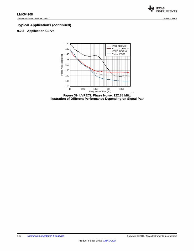
Frequency Offset (Hz)
Pha
se N
oise
(dB
c/H
z)
-170
-165
-160
-155
-150
-145
-140
-135
-130
1k 10k 100k 1M 10M
D001
VCO CLKoutXVCXO CLKout3,4VCXO OSCoutVCXO Direct
120
LMK04208SNAS684 –SEPTEMBER 2016 www.ti.com
Product Folder Links: LMK04208
Submit Documentation Feedback Copyright © 2016, Texas Instruments Incorporated
Typical Applications (continued)9.2.3 Application Curve
Figure 39. LVPECL Phase Noise, 122.88 MHzIllustration of Different Performance Depending on Signal Path
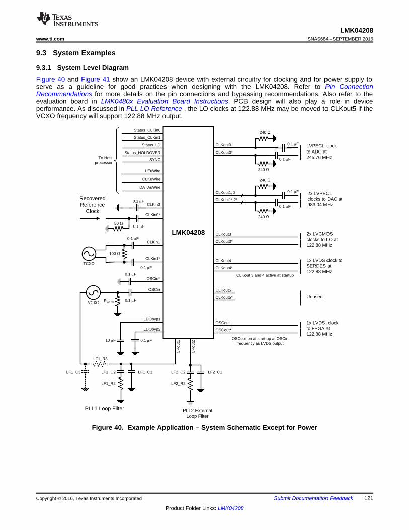
CP
out1
LEuWire
CLKuWire
DATAuWire
To Hostprocessor
LDObyp1
LDObyp2
10 PF 0.1 PF
LMK04208
OSCin
OSCin*
100 Ö
0.1 PF
0.1 PF
PLL1 Loop Filter
Rterm 0.1 PF
CLKin1
CLKin1*TCXO
50 Ö0.1 PF
0.1 PFCLKin0
CLKin0*
RecoveredReference
Clock
0.1 PF
VCXO
CP
out2
PLL2 ExternalLoop Filter
CLKout1*,2*
CLKout1, 2
0.1 PF
240 Ö
2x LVPECL clocks to DAC at 983.04 MHz
0.1 PF
240 Ö
2x LVCMOS clocks to LO at122.88 MHz
OSCout*
OSCout 1x LVDS clock to FPGA at 122.88 MHz
CLKout 3 and 4 active at startup
OSCout on at start-up at OSCin frequency as LVDS output
CLKout0*
CLKout0
0.1 PF
240 Ö
LVPECL clock to ADC at 245.76 MHz
0.1 PF
240 Ö
CLKout5*
CLKout5
Unused
CLKout3*
CLKout3
SYNC
Status_HOLDOVER
Status_LD
Status_CLKin1
Status_CLKin0
1x LVDS clock to SERDES at122.88 MHz
CLKout4*
CLKout4
LF1_C1LF1_C2
LF1_R2
LF2_C1LF2_C2
LF2_R2
LF1_C3
LF1_R3
121
LMK04208www.ti.com SNAS684 –SEPTEMBER 2016
Product Folder Links: LMK04208
Submit Documentation FeedbackCopyright © 2016, Texas Instruments Incorporated
9.3 System Examples
9.3.1 System Level DiagramFigure 40 and Figure 41 show an LMK04208 device with external circuitry for clocking and for power supply toserve as a guideline for good practices when designing with the LMK04208. Refer to Pin ConnectionRecommendations for more details on the pin connections and bypassing recommendations. Also refer to theevaluation board in LMK0480x Evaluation Board Instructions. PCB design will also play a role in deviceperformance. As discussed in PLL LO Reference , the LO clocks at 122.88 MHz may be moved to CLKout5 if theVCXO frequency will support 122.88 MHz output.
Figure 40. Example Application – System Schematic Except for Power
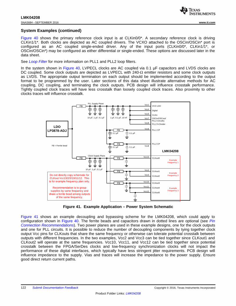
LMK04208
FB = Ferrite bead
Vcc13CLKout0
Vcc12CLKout5
Vcc11CLKout4
Vcc10CLKout3
Vcc9PLL2 N Divider
Vcc7 OSCin/OSCout/PLL2 Circuitry
Vcc6PLL1 CP
Vcc4Digital
Vcc3CLKout2
Vcc2CLKout1
Vcc1VCO LDO
Vcc8PLL2 CP
FB
FB
FB
FB
FB
Vcc5CLKin
PLL Supply Plane
Clock Supply Plane
LDOLP3878-ADJ
10 µF, 1 µF, 0.1 µF
10 µF, 1 µF, 0.1 µF 1 µF, 0.1 µF, 10 nF
0.1 µF
0.1 µF
0.1 µF
0.1 µF
FB
FB
Do not directly copy schematic for CLKout Vcc13/2/3/10/11/12. This is for example frequency plan only.
Recommendation is to group supplies by same frequency and
share a ferrite bead among outputs of the same frequency.
Example Frequency 1
Example Frequency 2
Example Frequency 3
122
LMK04208SNAS684 –SEPTEMBER 2016 www.ti.com
Product Folder Links: LMK04208
Submit Documentation Feedback Copyright © 2016, Texas Instruments Incorporated
System Examples (continued)Figure 40 shows the primary reference clock input is at CLKin0/0*. A secondary reference clock is drivingCLKin1/1*. Both clocks are depicted as AC coupled drivers. The VCXO attached to the OSCin/OSCin* port isconfigured as an AC coupled single-ended driver. Any of the input ports (CLKin0/0*, CLKin1/1*, orOSCin/OSCin*) may be configured as either differential or single-ended. These options are discussed later in thedata sheet.
See Loop Filter for more information on PLL1 and PLL2 loop filters.
In the system shown in Figure 40, LVPECL clocks are AC coupled via 0.1 µF capacitors and LVDS clocks areDC coupled. Some clock outputs are depicted as LVPECL with 240-Ω emitter resistors and some clock outputsas LVDS. The appropriate output termination on each output should be implemented according to the outputformat to be programmed by the user. Later sections of this data sheet illustrate alternative methods for ACcoupling, DC coupling, and terminating the clock outputs. PCB design will influence crosstalk performance.Tightly coupled clock traces will have less crosstalk than loosely coupled clock traces. Also proximity to otherclocks traces will influence crosstalk.
Figure 41. Example Application – Power System Schematic
Figure 41 shows an example decoupling and bypassing scheme for the LMK04208, which could apply toconfiguration shown in Figure 40. The ferrite beads and capacitors drawn in dotted lines are optional (see PinConnection Recommendations). Two power planes are used in these example designs, one for the clock outputsand one for PLL circuits. It is possible to reduce the number of decoupling components by tying together clockoutput Vcc pins for CLKouts that share the same frequency or otherwise can tolerate potential crosstalk betweenoutputs with different frequencies. In the two examples, Vcc2 and Vcc3 can be tied together since CLKout1 andCLKout2 will operate at the same frequencies. Vcc10, Vcc11, and Vcc12 can be tied together since potentialcrosstalk between the FPGA/SerDes clocks and low-frequency synchronization clocks will not impact theperformance of these digital interfaces, which typically have less stringent jitter requirements. PCB design willinfluence impedance to the supply. Vias and traces will increase the impedance to the power supply. Ensuregood direct return current paths.
123
LMK04208www.ti.com SNAS684 –SEPTEMBER 2016
Product Folder Links: LMK04208
Submit Documentation FeedbackCopyright © 2016, Texas Instruments Incorporated
9.4 Do's and Don'ts
9.4.1 LVCMOS Complementary vs. Non-Complementary Operation• TI recommends using a complementary LVCMOS output format such as LVCMOS (Norm/Inv) to reduce
switching noise and crosstalk when using LVCMOS.• If only a single LVCMOS output is required, the complementary LVCMOS output format can still be used by
leaving the unused LVCMOS output floating.• A non-complimentary format such as LVCMOS (Norm/Norm) is not recommended as increased switching
noise is present.
9.4.2 LVPECL OutputsWhen using an LVPECL output it is not recommended to place a capacitor to ground on the output as might bedone when using a capacitor input LC lowpass filter. The capacitor will appear as a short to the LVPECL outputdrivers which are able to supply large amounts of switching current. The effect of the LVPECL sourcing largeswitching currents can result in the following:1. Large switching currents through the Vcc pin of the LVPECL power supply resulting in more Vcc noise and
possible Vcc spikes.2. Large switching currents injected into the ground plane through the capacitor which could couple onto other
Vcc pins with bypass capacitors to ground resulting in more Vcc noise and possible Vcc spikes.
9.4.3 Sharing MICROWIRE (SPI) LinesWhen CLKuWire and DATAuWire toggle and an internal VCO mode is used, there may some spurious contenton the phase noise plot related to the frequency of the CLKuWire and DATAuWire pins.
124
LMK04208SNAS684 –SEPTEMBER 2016 www.ti.com
Product Folder Links: LMK04208
Submit Documentation Feedback Copyright © 2016, Texas Instruments Incorporated
10 Power Supply Recommendations
10.1 Pin Connection Recommendations
10.1.1 Vcc Pins and DecouplingAll Vcc pins must always be connected.
Integrated capacitance on the LMK04208 makes external high frequency decoupling capacitors (≤ 1 nF)unnecessary. The internal capacitance is more effective at filtering high frequency noise than off device bypasscapacitance because there is no bond wire inductance between the LMK04208 circuit and the bypass capacitor.
10.1.1.1 Vcc2, Vcc3, Vcc10, Vcc11, Vcc12, Vcc13 (CLKout Vccs)Each of these pins has an internal 200 pF of capacitance.
Ferrite beads may be used to reduce crosstalk between different clock output frequencies on the sameLMK04208 device. Ferrite beads placed between the power supply and a clock Vcc pin will reduce noisebetween the Vcc pin and the power supply. When several output clocks share the same frequency a single ferritebead can be used between the power supply and each same frequency CLKout Vcc pin.
When using ferrite beads on CLKout Vcc pins, consider the following guidelines to ensure the power supply willsource the needed switching current:• In most cases a ferrite bead may be placed and the internal capacitance is sufficient.• If a ferrite bead is used with a low frequency output (typically ≤ 30 MHz) and a high current switching clock
output format such as non-complementary LVCMOS or high swing LVPECL is used, then:– The ferrite bead can be removed to the lower impedance to the main power supply and bypass capacitors,
or– Localized capacitance can be placed between the ferrite bead and Vcc pin to support the switching
current.– Note: the decoupling capacitors used between the ferrite bead and a CLKout Vcc pin can permit high
frequency switching noise to couple through the capacitors into the ground plane and onto otherCLKout Vcc pins with decoupling capacitors. This can degrade crosstalk performance.
– TI recommends using a complementary LVCMOS output format such as LVCMOS (Norm/Inv) to reduceswitching noise and crosstalk when using LVCMOS. If only a single LVCMOS output is required, thecomplementary LVCMOS output format can still be used by leaving the unused LVCMOS output floating.
10.1.1.2 Vcc1 (VCO), Vcc4 (Digital), and Vcc9 (PLL2)Each of these pins has internal bypass capacitance.
Ferrite beads should not be used between these pins and the power supply/large bypass capacitors becausethese Vcc pins don’t produce much noise and a ferrite bead can cause phase noise disturbances andresonances.
The typical application diagram in Figure 41 shows all these Vccs connected to together to Vcc without a ferritebead.
10.1.1.3 Vcc6 (PLL1 Charge Pump) and Vcc8 (PLL2 Charge Pump)Each of these pins has an internal bypass capacitor.
Use of a ferrite bead between the power supply/large bypass capacitors and PLL1 is optional. PLL1 chargepump can be connected directly to Vcc along with Vcc1, Vcc4, and Vcc9. Depending on the application, a 0.1 µFcapacitor may be placed close to PLL1 charge pump Vcc pin.
A ferrite bead should be placed between the power supply/large bypass capacitors and Vcc8. Most applicationshave high PLL2 phase detector frequencies and (> 50 MHz) such that the internal bypassing is sufficient and aferrite bead can be used to isolate this switching noise from other circuits. For lower phase detector frequenciesa ferrite bead is optional and depending on application a 0.1 µF capacitor may be added on Vcc8.
125
LMK04208www.ti.com SNAS684 –SEPTEMBER 2016
Product Folder Links: LMK04208
Submit Documentation FeedbackCopyright © 2016, Texas Instruments Incorporated
Pin Connection Recommendations (continued)10.1.1.4 Vcc5 (CLKin), Vcc7 (OSCin and OSCout)Each of these pins has an internal 100 pF of capacitance. No ferrite bead should be placed between the powersupply/large bypass capacitors and Vcc5 or Vcc7.
These pins are unique since they supply an output clock and other circuitry.
Vcc5 supplies CLKin.
Vcc7 supplies OSCin, OSCout, and PLL2 circuitry.
Impacts of excessive noise on PLL2 circuitry may impact PLL2 DLD operation.
TI recommends using a complementary LVCMOS output format such as LVCMOS (Norm/Inv) to reduceswitching noise and crosstalk when using LVCMOS. If only a single LVCMOS output is required, thecomplementary LVCMOS output format can still be used by leaving the unused LVCMOS output floating.
10.1.2 LVPECL OutputsWhen using an LVPECL output it is not recommended to place a capacitor to ground on the output as might bedone when using a capacitor input LC lowpass filter. The capacitor will appear as a short to the LVPECL outputdrivers which are able to supply large amounts of switching current. The effect of the LVPECL sourcing largeswitching currents can result in:1. Large switching currents through the Vcc pin of the LVPECL power supply resulting in more Vcc noise and
possible Vcc spikes.2. Large switching currents injected into the ground plane through the capacitor which could couple onto other
Vcc pins with bypass capacitors to ground resulting in more Vcc noise and possible Vcc spikes.
10.1.3 Unused Clock OutputsLeave unused clock outputs floating and powered down.
10.1.4 Unused Clock InputsUnused clock inputs can be left floating.
10.1.5 LDO BypassThe LDObyp1 and LDObyp2 pins should be connected to GND through external capacitors, as shown inFigure 41.
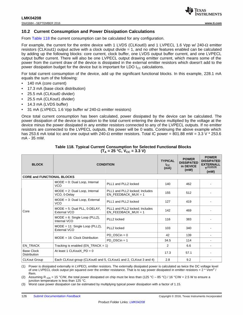
126
LMK04208SNAS684 –SEPTEMBER 2016 www.ti.com
Product Folder Links: LMK04208
Submit Documentation Feedback Copyright © 2016, Texas Instruments Incorporated
(1) Power is dissipated externally in LVPECL emitter resistors. The externally dissipated power is calculated as twice the DC voltage levelof one LVPECL clock output pin squared over the emitter resistance. That is to say power dissipated in emitter resistors = 2 * Vem2 /Rem.
(2) Assuming R θJA = 15 °C/W, the total power dissipated on chip must be less than (125 °C – 85 °C) / 16 °C/W = 2.5 W to ensure ajunction temperature is less than 125 °C.
(3) Worst case power dissipation can be estimated by multiplying typical power dissipation with a factor of 1.15.
10.2 Current Consumption and Power Dissipation CalculationsFrom Table 118 the current consumption can be calculated for any configuration.
For example, the current for the entire device with 1 LVDS (CLKout0) and 1 LVPECL 1.6 Vpp w/ 240-Ω emitterresistors (CLKout1) output active with a clock output divide = 1, and no other features enabled can be calculatedby adding up the following blocks: core current, clock buffer, one LVDS output buffer current, and one LVPECLoutput buffer current. There will also be one LVPECL output drawing emitter current, which means some of thepower from the current draw of the device is dissipated in the external emitter resistors which doesn't add to thepower dissipation budget for the device but is important for LDO ICC calculations.
For total current consumption of the device, add up the significant functional blocks. In this example, 228.1 mAequals the sum of the following:• 140 mA (core current)• 17.3 mA (base clock distribution)• 25.5 mA (CLKout0 divider)• 25.5 mA (CLKout1 divider)• 14.3 mA (LVDS buffer)• 31 mA (LVPECL 1.6 Vpp buffer w/ 240-Ω emitter resistors)
Once total current consumption has been calculated, power dissipated by the device can be calculated. Thepower dissipation of the device is equation to the total current entering the device multiplied by the voltage at thedevice minus the power dissipated in any emitter resistors connected to any of the LVPECL outputs. If no emitterresistors are connected to the LVPECL outputs, this power will be 0 watts. Continuing the above example whichhas 253.6 mA total Icc and one output with 240-Ω emitter resistors. Total IC power = 801.88 mW = 3.3 V * 253.6mA - 35 mW.
Table 118. Typical Current Consumption for Selected Functional Blocks(TA = 25 °C, VCC = 3.3 V)
BLOCK CONDITIONTYPICAL
ICC(mA)
POWERDISSIPATEDin DEVICE
(mW)
POWERDISSIPATEDEXTERNALL
Y (1) (2) (3)
(mW)CORE and FUNCTIONAL BLOCKS
Core
MODE = 0: Dual Loop, InternalVCO PLL1 and PLL2 locked 140 462 -
MODE = 2: Dual Loop, InternalVCO, 0-Delay
PLL1 and PLL2 locked; IncludesEN_FEEDBACK_MUX = 1 155 512 -
MODE = 3: Dual Loop, ExternalVCO PLL1 and PLL2 locked 127 419 -
MODE = 5: Dual PLL, 0-DELAY,External VCO
PLL1 and PLL2 locked; IncludesEN_FEEDBACK_MUX = 1 142 469 -
MODE = 6: Single Loop (PLL2),Internal VCO PLL2 locked 116 383 -
MODE = 11: Single Loop (PLL2),External VCO PLL2 locked 103 340 -
MODE = 16: Clock DistributionPD_OSCin = 0 42 139 -PD_OSCin = 1 34.5 114 -
EN_TRACK Tracking is enabled (EN_TRACK = 1) 2 6.6 -Base ClockDistribution
At least 1 CLKoutX_PD = 0 17.3 57.1 -
CLKout Group Each CLKout group (CLKout0 and 5, CLKout1 and 2, CLKout 3 and 4) 2.8 9.2 -
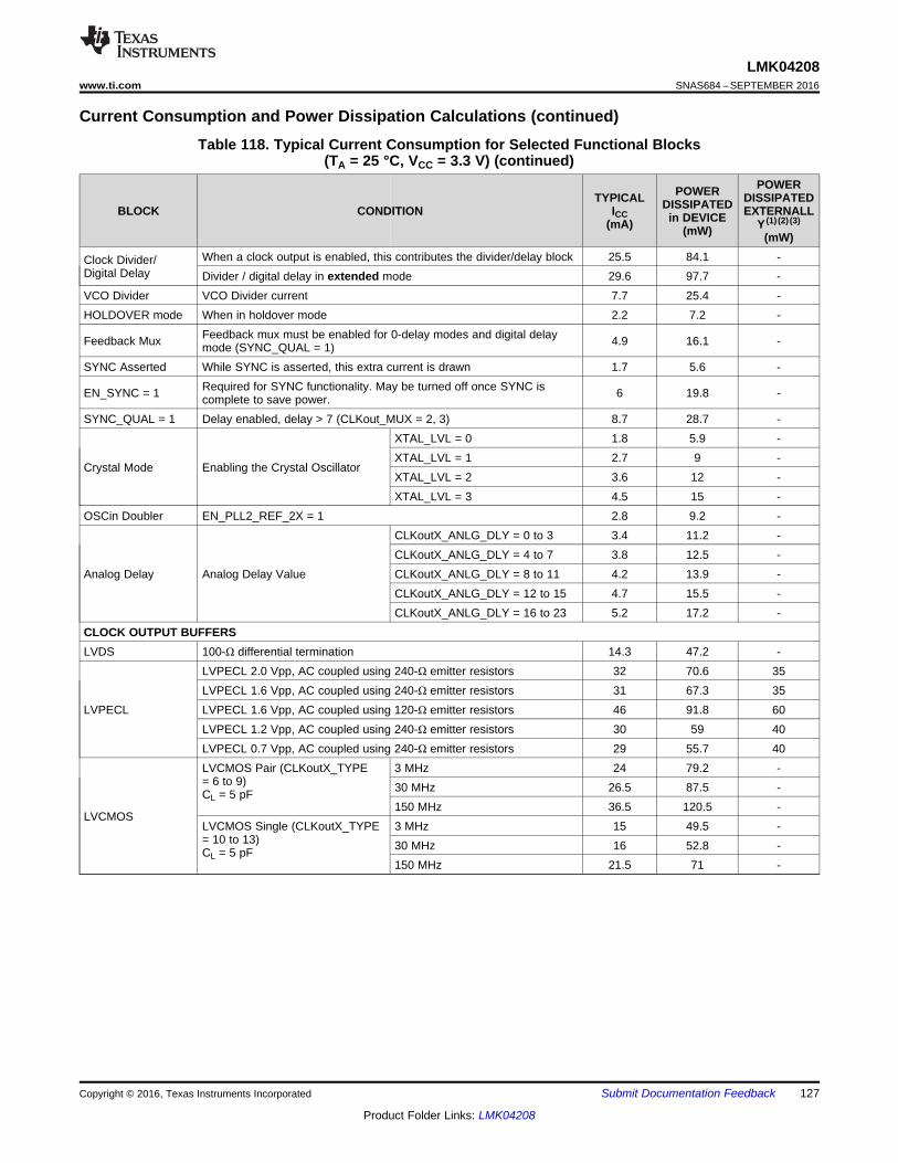
127
LMK04208www.ti.com SNAS684 –SEPTEMBER 2016
Product Folder Links: LMK04208
Submit Documentation FeedbackCopyright © 2016, Texas Instruments Incorporated
Current Consumption and Power Dissipation Calculations (continued)Table 118. Typical Current Consumption for Selected Functional Blocks
(TA = 25 °C, VCC = 3.3 V) (continued)
BLOCK CONDITIONTYPICAL
ICC(mA)
POWERDISSIPATEDin DEVICE
(mW)
POWERDISSIPATEDEXTERNALL
Y (1) (2) (3)
(mW)
Clock Divider/Digital Delay
When a clock output is enabled, this contributes the divider/delay block 25.5 84.1 -Divider / digital delay in extended mode 29.6 97.7 -
VCO Divider VCO Divider current 7.7 25.4 -HOLDOVER mode When in holdover mode 2.2 7.2 -
Feedback Mux Feedback mux must be enabled for 0-delay modes and digital delaymode (SYNC_QUAL = 1) 4.9 16.1 -
SYNC Asserted While SYNC is asserted, this extra current is drawn 1.7 5.6 -
EN_SYNC = 1 Required for SYNC functionality. May be turned off once SYNC iscomplete to save power. 6 19.8 -
SYNC_QUAL = 1 Delay enabled, delay > 7 (CLKout_MUX = 2, 3) 8.7 28.7 -
Crystal Mode Enabling the Crystal Oscillator
XTAL_LVL = 0 1.8 5.9 -XTAL_LVL = 1 2.7 9 -XTAL_LVL = 2 3.6 12 -XTAL_LVL = 3 4.5 15 -
OSCin Doubler EN_PLL2_REF_2X = 1 2.8 9.2 -
Analog Delay Analog Delay Value
CLKoutX_ANLG_DLY = 0 to 3 3.4 11.2 -CLKoutX_ANLG_DLY = 4 to 7 3.8 12.5 -CLKoutX_ANLG_DLY = 8 to 11 4.2 13.9 -CLKoutX_ANLG_DLY = 12 to 15 4.7 15.5 -CLKoutX_ANLG_DLY = 16 to 23 5.2 17.2 -
CLOCK OUTPUT BUFFERSLVDS 100-Ω differential termination 14.3 47.2 -
LVPECL
LVPECL 2.0 Vpp, AC coupled using 240-Ω emitter resistors 32 70.6 35LVPECL 1.6 Vpp, AC coupled using 240-Ω emitter resistors 31 67.3 35LVPECL 1.6 Vpp, AC coupled using 120-Ω emitter resistors 46 91.8 60LVPECL 1.2 Vpp, AC coupled using 240-Ω emitter resistors 30 59 40LVPECL 0.7 Vpp, AC coupled using 240-Ω emitter resistors 29 55.7 40
LVCMOS
LVCMOS Pair (CLKoutX_TYPE= 6 to 9)CL = 5 pF
3 MHz 24 79.2 -30 MHz 26.5 87.5 -150 MHz 36.5 120.5 -
LVCMOS Single (CLKoutX_TYPE= 10 to 13)CL = 5 pF
3 MHz 15 49.5 -30 MHz 16 52.8 -150 MHz 21.5 71 -
128
LMK04208SNAS684 –SEPTEMBER 2016 www.ti.com
Product Folder Links: LMK04208
Submit Documentation Feedback Copyright © 2016, Texas Instruments Incorporated
11 Layout
11.1 Layout GuidelinesPower consumption of the LMK04208 device can be high enough to require attention to thermal management.For reliability and performance reasons the die temperature should be limited to a maximum of 125 °C. That is,as an estimate, TA (ambient temperature) plus device power consumption times RθJA should not exceed 125 °C.
The package of the device has an exposed pad that provides the primary heat removal path as well as excellentelectrical grounding to a printed circuit board. To maximize the removal of heat from the package a thermal landpattern including multiple vias to a ground plane must be incorporated on the PCB within the footprint of thepackage. The exposed pad must be soldered down to ensure adequate heat conduction out of the package.
A recommended land and via pattern is shown at the end of the datasheet, Mechanical, Packaging, andOrderable Information. More information on soldering WQFN packages can be obtained fromwww.ti.com/packaging/.
To minimize junction temperature, TI recommends that a simple heat sink be built into the PCB (if the groundplane layer is not exposed). This is done by including a copper area on the opposite side of the PCB from thedevice. This copper area may be plated or solder coated to prevent corrosion, but should not have conformalcoating (if possible), which could provide thermal insulation.

CLKin and OSCin paths ± if differential input (preferred) route trace tightly coupled like clock outputs. If single ended, have at least 3 trace width (of CLKin/OSCin trace) separation from other RF traces.Example shown is hybrid for both differential and single ended ± not tightly couple to compromise for both configurations. RF Terminations should be placed as close to IC as possible. When using CLKin1 for high frequency input for external VCO or distribution, a 3 dB pi pad is suggested for termination.
)RU&/.RXW9FF¶VSODFHIHUULWHEHDGVRQWRSOD\HUFORVHWRSLQVWRFKRNH
high frequency noise from via.
Charge pump output ± shorter traces are betterPlace all resistors and caps closer to IC except a single capacitor next to VCXO. In a 2nd order filter place C1 close to VCXO Vtune pin. In a 3rd
and 4th order filter place C3 or C4 respectively close to VCXO.
Clock outputs ± differential signals, should be routed tightly coupled to minimize PCB crosstalTrace impedance and terminations should be designed according to output type being used (iLVDS, LVPECL...)
129
LMK04208www.ti.com SNAS684 –SEPTEMBER 2016
Product Folder Links: LMK04208
Submit Documentation FeedbackCopyright © 2016, Texas Instruments Incorporated
11.2 Layout Example
Figure 42. LMK04208 Layout Example
130
LMK04208SNAS684 –SEPTEMBER 2016 www.ti.com
Product Folder Links: LMK04208
Submit Documentation Feedback Copyright © 2016, Texas Instruments Incorporated
12 Device and Documentation Support
12.1 Device Support
12.1.1 Development SupportFor additional support, see the following:• Clock Architect (simulation): http://www.ti.com/lsds/ti/analog/webench/clock-architect.page• TICS Pro (EVM programming and register generation tool):
12.2 Documentation Support
12.2.1 Related DocumentationFor additional information, see the following:• AN-912 Common Data Transmission Parameters and their Definitions• AN-1939 Crystal Based Oscillator Design with the LMK04000 Family• AN-1865 Frequency Synthesis and Planning for PLL Architectures
12.3 Receiving Notification of Documentation UpdatesTo receive notification of documentation updates, navigate to the device product folder on ti.com. In the upperright corner, click on Alert me to register and receive a weekly digest of any product information that haschanged. For change details, review the revision history included in any revised document.
12.4 Community ResourcesThe following links connect to TI community resources. Linked contents are provided "AS IS" by the respectivecontributors. They do not constitute TI specifications and do not necessarily reflect TI's views; see TI's Terms ofUse.
TI E2E™ Online Community TI's Engineer-to-Engineer (E2E) Community. Created to foster collaborationamong engineers. At e2e.ti.com, you can ask questions, share knowledge, explore ideas and helpsolve problems with fellow engineers.
Design Support TI's Design Support Quickly find helpful E2E forums along with design support tools andcontact information for technical support.
12.5 TrademarksPLLatinum, E2E are trademarks of Texas Instruments.All other trademarks are the property of their respective owners.
12.6 Electrostatic Discharge CautionThese devices have limited built-in ESD protection. The leads should be shorted together or the device placed in conductive foamduring storage or handling to prevent electrostatic damage to the MOS gates.
12.7 GlossarySLYZ022 — TI Glossary.
This glossary lists and explains terms, acronyms, and definitions.
13 Mechanical, Packaging, and Orderable InformationThe following pages include mechanical, packaging, and orderable information. This information is the mostcurrent data available for the designated devices. This data is subject to change without notice and revision ofthis document. For browser-based versions of this data sheet, refer to the left-hand navigation.
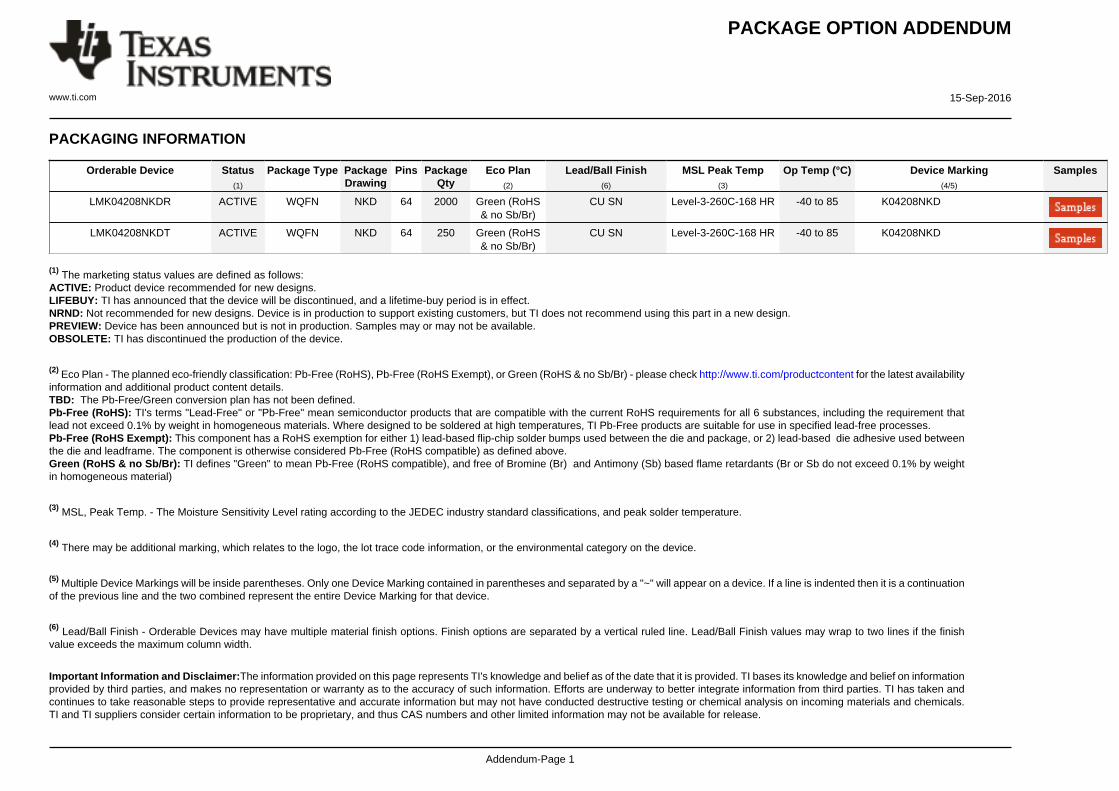
PACKAGE OPTION ADDENDUM
www.ti.com 15-Sep-2016
Addendum-Page 1
PACKAGING INFORMATION
Orderable Device Status(1)
Package Type PackageDrawing
Pins PackageQty
Eco Plan(2)
Lead/Ball Finish(6)
MSL Peak Temp(3)
Op Temp (°C) Device Marking(4/5)
Samples
LMK04208NKDR ACTIVE WQFN NKD 64 2000 Green (RoHS& no Sb/Br)
CU SN Level-3-260C-168 HR -40 to 85 K04208NKD
LMK04208NKDT ACTIVE WQFN NKD 64 250 Green (RoHS& no Sb/Br)
CU SN Level-3-260C-168 HR -40 to 85 K04208NKD
(1) The marketing status values are defined as follows:ACTIVE: Product device recommended for new designs.LIFEBUY: TI has announced that the device will be discontinued, and a lifetime-buy period is in effect.NRND: Not recommended for new designs. Device is in production to support existing customers, but TI does not recommend using this part in a new design.PREVIEW: Device has been announced but is not in production. Samples may or may not be available.OBSOLETE: TI has discontinued the production of the device.
(2) Eco Plan - The planned eco-friendly classification: Pb-Free (RoHS), Pb-Free (RoHS Exempt), or Green (RoHS & no Sb/Br) - please check http://www.ti.com/productcontent for the latest availabilityinformation and additional product content details.TBD: The Pb-Free/Green conversion plan has not been defined.Pb-Free (RoHS): TI's terms "Lead-Free" or "Pb-Free" mean semiconductor products that are compatible with the current RoHS requirements for all 6 substances, including the requirement thatlead not exceed 0.1% by weight in homogeneous materials. Where designed to be soldered at high temperatures, TI Pb-Free products are suitable for use in specified lead-free processes.Pb-Free (RoHS Exempt): This component has a RoHS exemption for either 1) lead-based flip-chip solder bumps used between the die and package, or 2) lead-based die adhesive used betweenthe die and leadframe. The component is otherwise considered Pb-Free (RoHS compatible) as defined above.Green (RoHS & no Sb/Br): TI defines "Green" to mean Pb-Free (RoHS compatible), and free of Bromine (Br) and Antimony (Sb) based flame retardants (Br or Sb do not exceed 0.1% by weightin homogeneous material)
(3) MSL, Peak Temp. - The Moisture Sensitivity Level rating according to the JEDEC industry standard classifications, and peak solder temperature.
(4) There may be additional marking, which relates to the logo, the lot trace code information, or the environmental category on the device.
(5) Multiple Device Markings will be inside parentheses. Only one Device Marking contained in parentheses and separated by a "~" will appear on a device. If a line is indented then it is a continuationof the previous line and the two combined represent the entire Device Marking for that device.
(6) Lead/Ball Finish - Orderable Devices may have multiple material finish options. Finish options are separated by a vertical ruled line. Lead/Ball Finish values may wrap to two lines if the finishvalue exceeds the maximum column width.
Important Information and Disclaimer:The information provided on this page represents TI's knowledge and belief as of the date that it is provided. TI bases its knowledge and belief on informationprovided by third parties, and makes no representation or warranty as to the accuracy of such information. Efforts are underway to better integrate information from third parties. TI has taken andcontinues to take reasonable steps to provide representative and accurate information but may not have conducted destructive testing or chemical analysis on incoming materials and chemicals.TI and TI suppliers consider certain information to be proprietary, and thus CAS numbers and other limited information may not be available for release.
PACKAGE OPTION ADDENDUM
www.ti.com 15-Sep-2016
Addendum-Page 2
In no event shall TI's liability arising out of such information exceed the total purchase price of the TI part(s) at issue in this document sold by TI to Customer on an annual basis.
TAPE AND REEL INFORMATION
*All dimensions are nominal
Device PackageType
PackageDrawing
Pins SPQ ReelDiameter
(mm)
ReelWidth
W1 (mm)
A0(mm)
B0(mm)
K0(mm)
P1(mm)
W(mm)
Pin1Quadrant
LMK04208NKDR WQFN NKD 64 2000 330.0 16.4 9.3 9.3 1.3 12.0 16.0 Q1
LMK04208NKDT WQFN NKD 64 250 178.0 16.4 9.3 9.3 1.3 12.0 16.0 Q1
PACKAGE MATERIALS INFORMATION
www.ti.com 20-Sep-2016
Pack Materials-Page 1
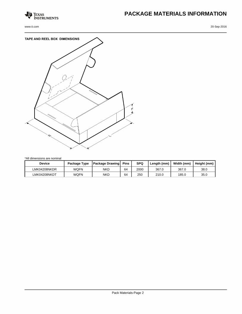
*All dimensions are nominal
Device Package Type Package Drawing Pins SPQ Length (mm) Width (mm) Height (mm)
LMK04208NKDR WQFN NKD 64 2000 367.0 367.0 38.0
LMK04208NKDT WQFN NKD 64 250 210.0 185.0 35.0
PACKAGE MATERIALS INFORMATION
www.ti.com 20-Sep-2016
Pack Materials-Page 2
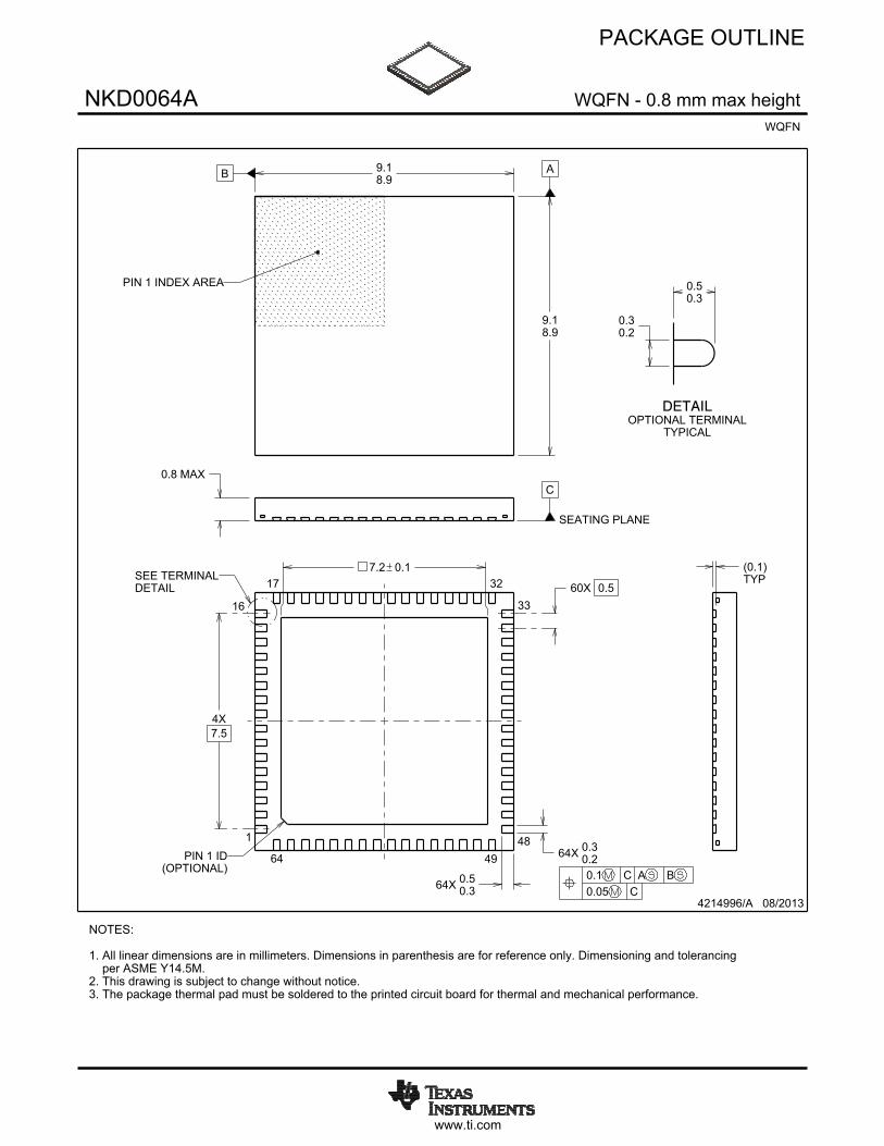
www.ti.com
PACKAGE OUTLINE
C
64X 0.30.2
7.2 0.1
60X 0.5
64X 0.50.3
0.8 MAX
4X7.5
A
9.18.9
B 9.18.9
0.30.2
0.50.3
(0.1)TYP
4214996/A 08/2013
WQFN - 0.8 mm max heightNKD0064AWQFN
PIN 1 INDEX AREA
SEATING PLANE
1
16 33
48
17 32
64 49(OPTIONAL)
PIN 1 ID
SEE TERMINALDETAIL
NOTES: 1. All linear dimensions are in millimeters. Dimensions in parenthesis are for reference only. Dimensioning and tolerancing per ASME Y14.5M.2. This drawing is subject to change without notice. 3. The package thermal pad must be soldered to the printed circuit board for thermal and mechanical performance.
0.1 C A B0.05 C
SCALE 1.600
DETAILOPTIONAL TERMINAL
TYPICAL
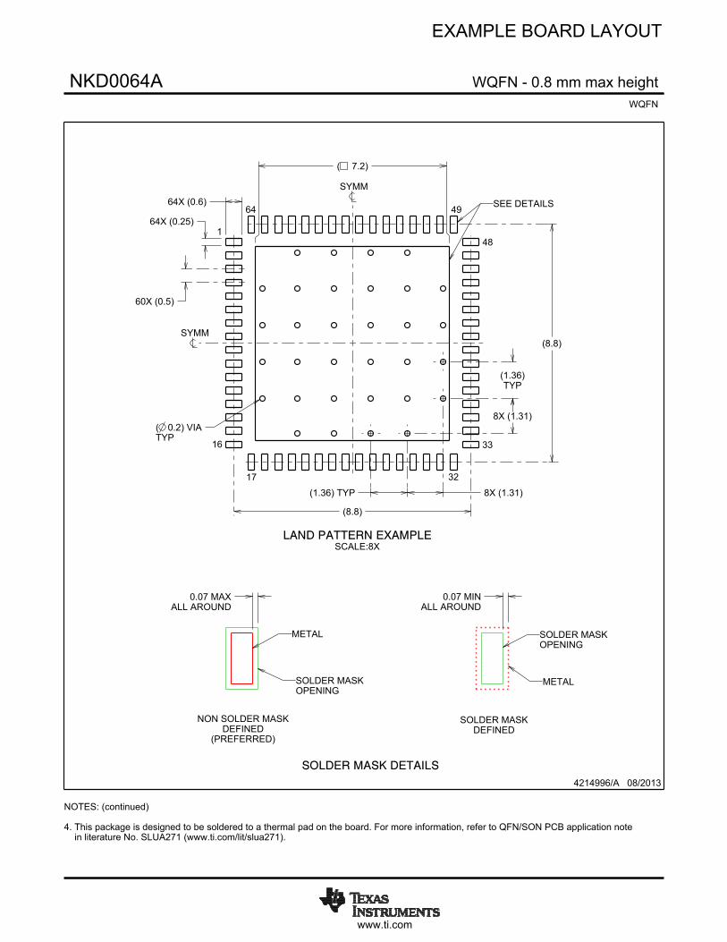
www.ti.com
EXAMPLE BOARD LAYOUT
( 7.2)
0.07 MINALL AROUND
0.07 MAXALL AROUND
64X (0.6)
64X (0.25)
(8.8)
(8.8)
60X (0.5)
( ) VIATYP
0.2
(1.36)TYP
8X (1.31)
(1.36) TYP 8X (1.31)
4214996/A 08/2013
WQFN - 0.8 mm max heightNKD0064AWQFN
SYMM
SEE DETAILS
1
16
17 32
33
48
4964
SYMM
LAND PATTERN EXAMPLESCALE:8X
NOTES: (continued) 4. This package is designed to be soldered to a thermal pad on the board. For more information, refer to QFN/SON PCB application note in literature No. SLUA271 (www.ti.com/lit/slua271).
SOLDER MASKOPENING
METAL
SOLDER MASKDEFINED
METAL
SOLDER MASKOPENING
SOLDER MASK DETAILS
NON SOLDER MASKDEFINED
(PREFERRED)
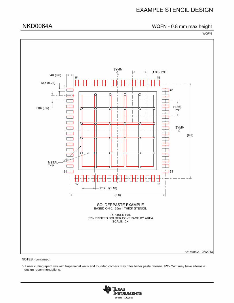
www.ti.com
EXAMPLE STENCIL DESIGN
(8.8)
64X (0.6)
64X (0.25)
25X (1.16)
(8.8)
60X (0.5)
(1.36) TYP
(1.36)TYP
4214996/A 08/2013
WQFN - 0.8 mm max heightNKD0064AWQFN
NOTES: (continued) 5. Laser cutting apertures with trapezoidal walls and rounded corners may offer better paste release. IPC-7525 may have alternate design recommendations.
SYMM
METALTYP
SOLDERPASTE EXAMPLEBASED ON 0.125mm THICK STENCIL
EXPOSED PAD
65% PRINTED SOLDER COVERAGE BY AREASCALE:10X
1
16
17 32
33
48
4964
SYMM
IMPORTANT NOTICE
Texas Instruments Incorporated and its subsidiaries (TI) reserve the right to make corrections, enhancements, improvements and otherchanges to its semiconductor products and services per JESD46, latest issue, and to discontinue any product or service per JESD48, latestissue. Buyers should obtain the latest relevant information before placing orders and should verify that such information is current andcomplete. All semiconductor products (also referred to herein as “components”) are sold subject to TI’s terms and conditions of salesupplied at the time of order acknowledgment.TI warrants performance of its components to the specifications applicable at the time of sale, in accordance with the warranty in TI’s termsand conditions of sale of semiconductor products. Testing and other quality control techniques are used to the extent TI deems necessaryto support this warranty. Except where mandated by applicable law, testing of all parameters of each component is not necessarilyperformed.TI assumes no liability for applications assistance or the design of Buyers’ products. Buyers are responsible for their products andapplications using TI components. To minimize the risks associated with Buyers’ products and applications, Buyers should provideadequate design and operating safeguards.TI does not warrant or represent that any license, either express or implied, is granted under any patent right, copyright, mask work right, orother intellectual property right relating to any combination, machine, or process in which TI components or services are used. Informationpublished by TI regarding third-party products or services does not constitute a license to use such products or services or a warranty orendorsement thereof. Use of such information may require a license from a third party under the patents or other intellectual property of thethird party, or a license from TI under the patents or other intellectual property of TI.Reproduction of significant portions of TI information in TI data books or data sheets is permissible only if reproduction is without alterationand is accompanied by all associated warranties, conditions, limitations, and notices. TI is not responsible or liable for such altereddocumentation. Information of third parties may be subject to additional restrictions.Resale of TI components or services with statements different from or beyond the parameters stated by TI for that component or servicevoids all express and any implied warranties for the associated TI component or service and is an unfair and deceptive business practice.TI is not responsible or liable for any such statements.Buyer acknowledges and agrees that it is solely responsible for compliance with all legal, regulatory and safety-related requirementsconcerning its products, and any use of TI components in its applications, notwithstanding any applications-related information or supportthat may be provided by TI. Buyer represents and agrees that it has all the necessary expertise to create and implement safeguards whichanticipate dangerous consequences of failures, monitor failures and their consequences, lessen the likelihood of failures that might causeharm and take appropriate remedial actions. Buyer will fully indemnify TI and its representatives against any damages arising out of the useof any TI components in safety-critical applications.In some cases, TI components may be promoted specifically to facilitate safety-related applications. With such components, TI’s goal is tohelp enable customers to design and create their own end-product solutions that meet applicable functional safety standards andrequirements. Nonetheless, such components are subject to these terms.No TI components are authorized for use in FDA Class III (or similar life-critical medical equipment) unless authorized officers of the partieshave executed a special agreement specifically governing such use.Only those TI components which TI has specifically designated as military grade or “enhanced plastic” are designed and intended for use inmilitary/aerospace applications or environments. Buyer acknowledges and agrees that any military or aerospace use of TI componentswhich have not been so designated is solely at the Buyer's risk, and that Buyer is solely responsible for compliance with all legal andregulatory requirements in connection with such use.TI has specifically designated certain components as meeting ISO/TS16949 requirements, mainly for automotive use. In any case of use ofnon-designated products, TI will not be responsible for any failure to meet ISO/TS16949.
Products ApplicationsAudio www.ti.com/audio Automotive and Transportation www.ti.com/automotiveAmplifiers amplifier.ti.com Communications and Telecom www.ti.com/communicationsData Converters dataconverter.ti.com Computers and Peripherals www.ti.com/computersDLP® Products www.dlp.com Consumer Electronics www.ti.com/consumer-appsDSP dsp.ti.com Energy and Lighting www.ti.com/energyClocks and Timers www.ti.com/clocks Industrial www.ti.com/industrialInterface interface.ti.com Medical www.ti.com/medicalLogic logic.ti.com Security www.ti.com/securityPower Mgmt power.ti.com Space, Avionics and Defense www.ti.com/space-avionics-defenseMicrocontrollers microcontroller.ti.com Video and Imaging www.ti.com/videoRFID www.ti-rfid.comOMAP Applications Processors www.ti.com/omap TI E2E Community e2e.ti.comWireless Connectivity www.ti.com/wirelessconnectivity
Mailing Address: Texas Instruments, Post Office Box 655303, Dallas, Texas 75265Copyright © 2016, Texas Instruments Incorporated


![IRU * WHFKQRORJLHV ,R7 · 2swlpl]dwlrq dqg 5hvrxufh 0dqdjhphqw lq 120$ :luhohvv 1hwzrunv 6xssruwlqj 5hdo dqg 1rq uhdo 7lph 6huylfh %xqgolqj 0xowlsoh 6huylfhv 5hdo 7lph](https://img.pdfslide.us/doc/110x75/5f57ffe3c50aa64f5e184bef/iru-whfkqrorjlhv-r7-2swlpldwlrq-dqg-5hvrxufh-0dqdjhphqw-lq-120-luhohvv-1hwzrunv.jpg)