Embed Size (px)
Citation preview
OUT
V-
+IN
V+
-IN
+ -
1
2
3
5
4
V+
1
2
3
4 5
6
7
8N/C
-IN
+IN
V-
N/C
OUT
N/C
-
+
LMH6624
www.ti.com SNOSA42F –NOVEMBER 2002–REVISED MARCH 2013
LMH6624/LMH6626 Single/Dual Ultra Low Noise Wideband Operational AmplifierCheck for Samples: LMH6624
1FEATURES DESCRIPTIONThe LMH6624/LMH6626 offer wide bandwidth
2• VS = ±6V, TA = 25°C, AV = 20, (Typical values(1.5GHz for single, 1.3GHz for dual) with very lowunless specified)input noise (0.92nV/√Hz, 2.3pA/√Hz) and ultra low dc
• Gain Bandwidth (LMH6624) 1.5GHz errors (100μV VOS, ±0.1μV/°C drift) providing very• Input Voltage Noise 0.92nV/√Hz precise operational amplifiers with wide dynamic
range. This enables the user to achieve closed-loop• Input Offset Voltage (limit over temp) 700µVgains of greater than 10, in both inverting and non-
• Slew Rate 350V/μs inverting configurations.• Slew Rate (AV = 10) 400V/μs
The LMH6624 (single) and LMH6626’s (dual)• HD2 @ f = 10MHz, RL = 100Ω −63dBc traditional voltage feedback topology provide the• HD3 @ f = 10MHz, RL = 100Ω −80dBc following benefits: balanced inputs, low offset voltage
and offset current, very low offset drift, 81dB open• Supply Voltage Range (dual supply) ±2.5V toloop gain, 95dB common mode rejection ratio, and±6V88dB power supply rejection ratio.
• Supply Voltage Range (single supply) +5V toThe LMH6624/LMH6626 operate from ± 2.5V to ± 6V+12Vin dual supply mode and from +5V to +12V in single• Improved Replacement for the CLC425 supply configuration.
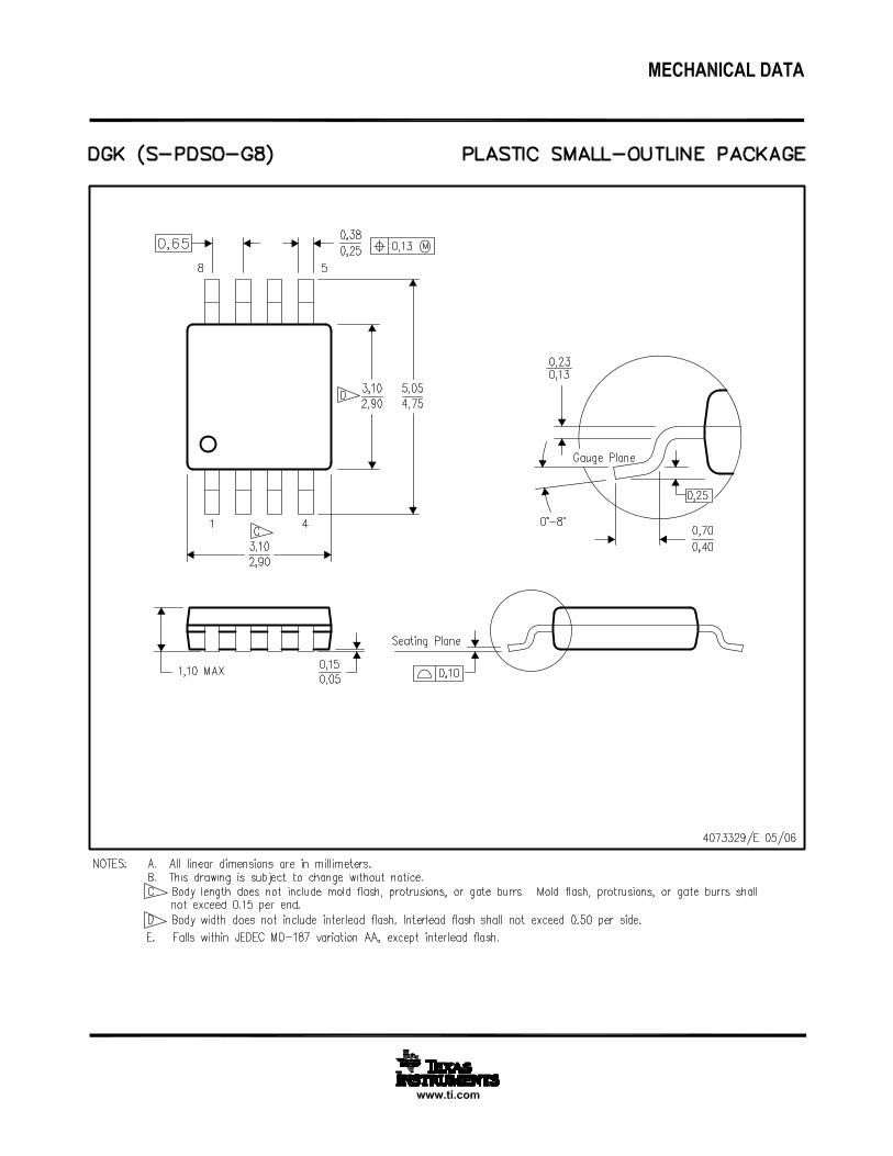
(LMH6624)LMH6624 is offered in SOT-23-5 and SOIC-8• Stable for Closed Loop |AV| ≥ 10packages.
The LMH6626 is offered in SOIC-8 and VSSOP-8APPLICATIONSpackages.• Instrumentation Sense Amplifiers
• Ultrasound Pre-amps• Magnetic Tape & Disk Pre-amps• Wide band active filters• Professional Audio Systems• Opto-electronics• Medical Diagnostic Systems
Connection Diagram
LMH6624 5-Pin SOT-23 LMH6624 8-Pin SOIC LMH6626 8-Pin SOIC/VSSOP
Figure 1. Top View Figure 2. Top View Figure 3. Top View
1
Please be aware that an important notice concerning availability, standard warranty, and use in critical applications ofTexas Instruments semiconductor products and disclaimers thereto appears at the end of this data sheet.
2All trademarks are the property of their respective owners.
PRODUCTION DATA information is current as of publication date. Copyright © 2002–2013, Texas Instruments IncorporatedProducts conform to specifications per the terms of the TexasInstruments standard warranty. Production processing does notnecessarily include testing of all parameters.
LMH6624
SNOSA42F –NOVEMBER 2002–REVISED MARCH 2013 www.ti.com
These devices have limited built-in ESD protection. The leads should be shorted together or the device placed in conductive foamduring storage or handling to prevent electrostatic damage to the MOS gates.
Absolute Maximum Ratings (1)
ESD Tolerance
Human Body Model 2000V (2)
Machine Model 200V (3)
VIN Differential ±1.2V
Supply Voltage (V+ - V−) 13.2V
Voltage at Input pins V+ +0.5V, V− −0.5V
Soldering Information
Infrared or Convection (20 sec.) 235°C
Wave Soldering (10 sec.) 260°C
Storage Temperature Range −65°C to +150°C
Junction Temperature (4), (5) +150°C
(1) Absolute maximum ratings indicate limits beyond which damage to the device may occur. Operating Ratings indicate conditions forwhich the device is intended to be functional, but specific performance is not ensured. For ensured specifications and the testconditions, see the Electrical Characteristics.
(2) Human body model, 1.5kΩ in series with 100pF.(3) Machine Model, 0Ω in series with 200pF.(4) Applies to both single-supply and split-supply operation. Continuous short circuit operation at elevated ambient temperature can result in
exceeding the maximum allowed junction temperature of 150°C.(5) The maximum power dissipation is a function of TJ(MAX), θJA, and TA. The maximum allowable power dissipation at any ambient
temperature is PD = (TJ(MAX) - TA)/ θJA . All numbers apply for packages soldered directly onto a PC board.
Operating Ratings (1)
Operating Temperature Range(2), (3) −40°C to +125°C
Package Thermal Resistance (θJA) (3)
SOIC-8 166°C/W
SOT23–5 265°C/W
VSSOP-8 235°C/W
(1) Absolute maximum ratings indicate limits beyond which damage to the device may occur. Operating Ratings indicate conditions forwhich the device is intended to be functional, but specific performance is not ensured. For ensured specifications and the testconditions, see the Electrical Characteristics.
(2) Applies to both single-supply and split-supply operation. Continuous short circuit operation at elevated ambient temperature can result inexceeding the maximum allowed junction temperature of 150°C.
(3) The maximum power dissipation is a function of TJ(MAX), θJA, and TA. The maximum allowable power dissipation at any ambienttemperature is PD = (TJ(MAX) - TA)/ θJA . All numbers apply for packages soldered directly onto a PC board.
2 Submit Documentation Feedback Copyright © 2002–2013, Texas Instruments Incorporated
Product Folder Links: LMH6624
LMH6624
www.ti.com SNOSA42F –NOVEMBER 2002–REVISED MARCH 2013
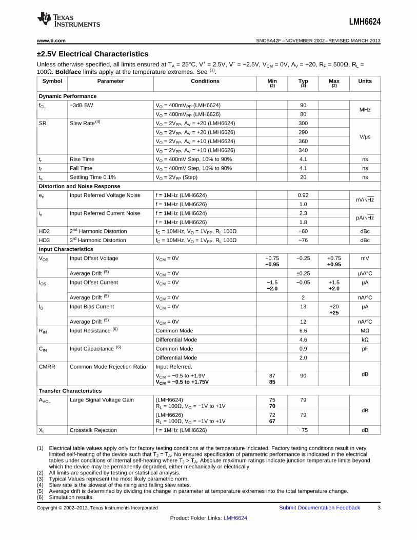
±2.5V Electrical CharacteristicsUnless otherwise specified, all limits ensured at TA = 25°C, V+ = 2.5V, V− = −2.5V, VCM = 0V, AV = +20, RF = 500Ω, RL =100Ω. Boldface limits apply at the temperature extremes. See (1).
Symbol Parameter Conditions Min Typ Max Units(2) (3) (2)
Dynamic Performance
fCL −3dB BW VO = 400mVPP (LMH6624) 90MHz
VO = 400mVPP (LMH6626) 80
SR Slew Rate (4) VO = 2VPP, AV = +20 (LMH6624) 300
VO = 2VPP, AV = +20 (LMH6626) 290V/μs
VO = 2VPP, AV = +10 (LMH6624) 360
VO = 2VPP, AV = +10 (LMH6626) 340
tr Rise Time VO = 400mV Step, 10% to 90% 4.1 ns
tf Fall Time VO = 400mV Step, 10% to 90% 4.1 ns
ts Settling Time 0.1% VO = 2VPP (Step) 20 ns
Distortion and Noise Response
en Input Referred Voltage Noise f = 1MHz (LMH6624) 0.92nV/√Hz
f = 1MHz (LMH6626) 1.0
in Input Referred Current Noise f = 1MHz (LMH6624) 2.3pA/√Hz
f = 1MHz (LMH6626) 1.8
HD2 2nd Harmonic Distortion fC = 10MHz, VO = 1VPP, RL 100Ω −60 dBc
HD3 3rd Harmonic Distortion fC = 10MHz, VO = 1VPP, RL 100Ω −76 dBc
Input Characteristics
VOS Input Offset Voltage VCM = 0V −0.75 −0.25 +0.75 mV−0.95 +0.95
Average Drift (5) VCM = 0V ±0.25 μV/°C
IOS Input Offset Current VCM = 0V −1.5 −0.05 +1.5 μA−2.0 +2.0
Average Drift (5) VCM = 0V 2 nA/°C
IB Input Bias Current VCM = 0V 13 +20 μA+25
Average Drift (5) VCM = 0V 12 nA/°C
RIN Input Resistance (6) Common Mode 6.6 MΩDifferential Mode 4.6 kΩ
CIN Input Capacitance (6) Common Mode 0.9 pF
Differential Mode 2.0
CMRR Common Mode Rejection Ratio Input Referred,dBVCM = −0.5 to +1.9V 87 90
VCM = −0.5 to +1.75V 85
Transfer Characteristics
AVOL Large Signal Voltage Gain (LMH6624) 75 79RL = 100Ω, VO = −1V to +1V 70
dB(LMH6626) 72 79RL = 100Ω, VO = −1V to +1V 67
Xt Crosstalk Rejection f = 1MHz (LMH6626) −75 dB
(1) Electrical table values apply only for factory testing conditions at the temperature indicated. Factory testing conditions result in verylimited self-heating of the device such that TJ = TA. No ensured specification of parametric performance is indicated in the electricaltables under conditions of internal self-heating where TJ > TA. Absolute maximum ratings indicate junction temperature limits beyondwhich the device may be permanently degraded, either mechanically or electrically.
(2) All limits are specified by testing or statistical analysis.(3) Typical Values represent the most likely parametric norm.(4) Slew rate is the slowest of the rising and falling slew rates.(5) Average drift is determined by dividing the change in parameter at temperature extremes into the total temperature change.(6) Simulation results.
Copyright © 2002–2013, Texas Instruments Incorporated Submit Documentation Feedback 3
Product Folder Links: LMH6624
LMH6624
SNOSA42F –NOVEMBER 2002–REVISED MARCH 2013 www.ti.com
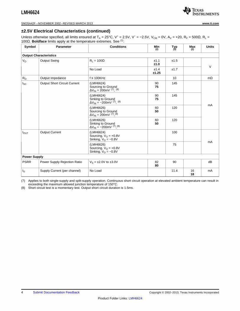
±2.5V Electrical Characteristics (continued)Unless otherwise specified, all limits ensured at TA = 25°C, V+ = 2.5V, V− = −2.5V, VCM = 0V, AV = +20, RF = 500Ω, RL =100Ω. Boldface limits apply at the temperature extremes. See (1).
Symbol Parameter Conditions Min Typ Max Units(2) (3) (2)
Output Characteristics
VO Output Swing RL = 100Ω ±1.1 ±1.5±1.0
VNo Load ±1.4 ±1.7
±1.25
RO Output Impedance f ≤ 100KHz 10 mΩISC Output Short Circuit Current (LMH6624) 90 145
Sourcing to Ground 75ΔVIN = 200mV (7), (8)
(LMH6624) 90 145Sinking to Ground 75ΔVIN = −200mV (7), (8)
mA(LMH6626) 60 120Sourcing to Ground 50ΔVIN = 200mV (7), (8)
(LMH6626) 60 120Sinking to Ground 50ΔVIN = −200mV (7), (8)
IOUT Output Current (LMH6624) 100Sourcing, VO = +0.8VSinking, VO = −0.8V
mA(LMH6626) 75Sourcing, VO = +0.8VSinking, VO = −0.8V
Power Supply
PSRR Power Supply Rejection Ratio VS = ±2.0V to ±3.0V 82 90 dB80
IS Supply Current (per channel) No Load 11.4 16 mA18
(7) Applies to both single-supply and split-supply operation. Continuous short circuit operation at elevated ambient temperature can result inexceeding the maximum allowed junction temperature of 150°C.
(8) Short circuit test is a momentary test. Output short circuit duration is 1.5ms.
4 Submit Documentation Feedback Copyright © 2002–2013, Texas Instruments Incorporated
Product Folder Links: LMH6624
LMH6624
www.ti.com SNOSA42F –NOVEMBER 2002–REVISED MARCH 2013
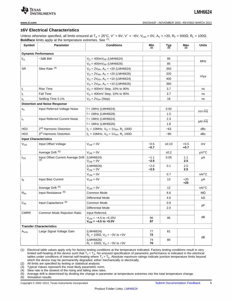
±6V Electrical CharacteristicsUnless otherwise specified, all limits ensured at TA = 25°C, V+ = 6V, V− = −6V, VCM = 0V, AV = +20, RF = 500Ω, RL = 100Ω.Boldface limits apply at the temperature extremes. See (1).
Symbol Parameter Conditions Min Typ Max Units(2) (3) (2)
Dynamic Performance
fCL −3dB BW VO = 400mVPP (LMH6624) 95MHz
VO = 400mVPP (LMH6626) 85
SR Slew Rate (4) VO = 2VPP, AV = +20 (LMH6624) 350
VO = 2VPP, AV = +20 (LMH6626) 320V/μs
VO = 2VPP, AV = +10 (LMH6624) 400
VO = 2VPP, AV = +10 (LMH6626) 360
tr Rise Time VO = 400mV Step, 10% to 90% 3.7 ns
tf Fall Time VO = 400mV Step, 10% to 90% 3.7 ns
ts Settling Time 0.1% VO = 2VPP (Step) 18 ns
Distortion and Noise Response
en Input Referred Voltage Noise f = 1MHz (LMH6624) 0.92nV/√Hz
f = 1MHz (LMH6626) 1.0
in Input Referred Current Noise f = 1MHz (LMH6624) 2.3pA/√Hz
f = 1MHz (LMH6626) 1.8
HD2 2nd Harmonic Distortion fC = 10MHz, VO = 1VPP, RL 100Ω −63 dBc
HD3 3rd Harmonic Distortion fC = 10MHz, VO = 1VPP, RL 100Ω −80 dBc
Input Characteristics
VOS Input Offset Voltage VCM = 0V −0.5 ±0.10 +0.5 mV−0.7 +0.7
Average Drift (5) VCM = 0V ±0.2 μV/°C
IOS Input Offset Current Average Drift (LMH6624) −1.1 0.05 1.1 μA(5) VCM = 0V −2.5 2.5
(LMH6626) −2.0 0.1 2.0VCM = 0V −2.5 2.5
VCM = 0V 0.7 nA/°C
IB Input Bias Current VCM = 0V 13 +20 μA+25
Average Drift (5) VCM = 0V 12 nA/°C
RIN Input Resistance (6) Common Mode 6.6 MΩDifferential Mode 4.6 kΩ
CIN Input Capacitance (6) Common Mode 0.9pF
Differential Mode 2.0
CMRR Common Mode Rejection Ratio Input Referred,dBVCM = −4.5 to +5.25V 90 95
VCM = −4.5 to +5.0V 87
Transfer Characteristics
AVOL Large Signal Voltage Gain (LMH6624) 77 81RL = 100Ω, VO = −3V to +3V 72
dB(LMH6626) 74 80RL = 100Ω, VO = −3V to +3V 70
(1) Electrical table values apply only for factory testing conditions at the temperature indicated. Factory testing conditions result in verylimited self-heating of the device such that TJ = TA. No ensured specification of parametric performance is indicated in the electricaltables under conditions of internal self-heating where TJ > TA. Absolute maximum ratings indicate junction temperature limits beyondwhich the device may be permanently degraded, either mechanically or electrically.
(2) All limits are specified by testing or statistical analysis.(3) Typical Values represent the most likely parametric norm.(4) Slew rate is the slowest of the rising and falling slew rates.(5) Average drift is determined by dividing the change in parameter at temperature extremes into the total temperature change.(6) Simulation results.
Copyright © 2002–2013, Texas Instruments Incorporated Submit Documentation Feedback 5
Product Folder Links: LMH6624
LMH6624
SNOSA42F –NOVEMBER 2002–REVISED MARCH 2013 www.ti.com
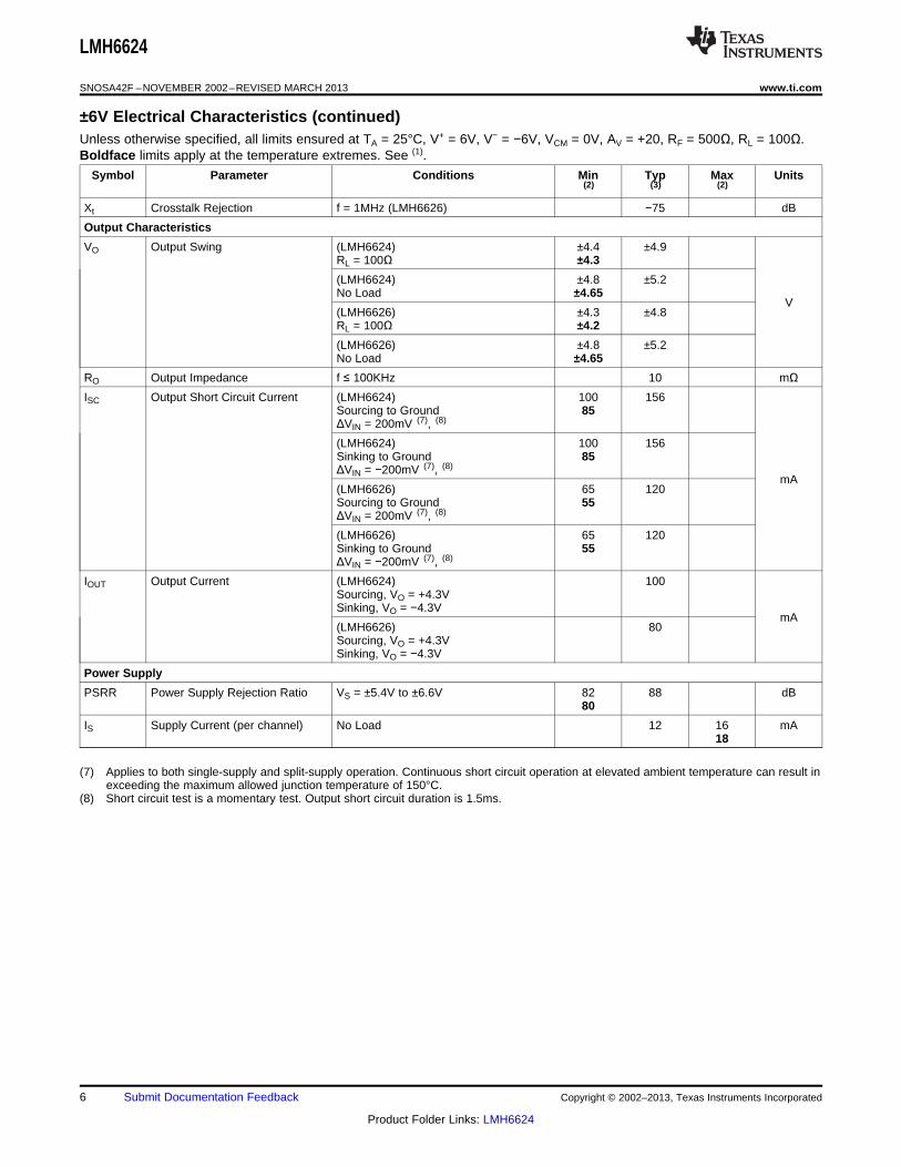
±6V Electrical Characteristics (continued)Unless otherwise specified, all limits ensured at TA = 25°C, V+ = 6V, V− = −6V, VCM = 0V, AV = +20, RF = 500Ω, RL = 100Ω.Boldface limits apply at the temperature extremes. See (1).
Symbol Parameter Conditions Min Typ Max Units(2) (3) (2)
Xt Crosstalk Rejection f = 1MHz (LMH6626) −75 dB
Output Characteristics
VO Output Swing (LMH6624) ±4.4 ±4.9RL = 100Ω ±4.3
(LMH6624) ±4.8 ±5.2No Load ±4.65
V(LMH6626) ±4.3 ±4.8RL = 100Ω ±4.2
(LMH6626) ±4.8 ±5.2No Load ±4.65
RO Output Impedance f ≤ 100KHz 10 mΩISC Output Short Circuit Current (LMH6624) 100 156
Sourcing to Ground 85ΔVIN = 200mV (7), (8)
(LMH6624) 100 156Sinking to Ground 85ΔVIN = −200mV (7), (8)
mA(LMH6626) 65 120Sourcing to Ground 55ΔVIN = 200mV (7), (8)
(LMH6626) 65 120Sinking to Ground 55ΔVIN = −200mV (7), (8)
IOUT Output Current (LMH6624) 100Sourcing, VO = +4.3VSinking, VO = −4.3V
mA(LMH6626) 80Sourcing, VO = +4.3VSinking, VO = −4.3V
Power Supply
PSRR Power Supply Rejection Ratio VS = ±5.4V to ±6.6V 82 88 dB80
IS Supply Current (per channel) No Load 12 16 mA18
(7) Applies to both single-supply and split-supply operation. Continuous short circuit operation at elevated ambient temperature can result inexceeding the maximum allowed junction temperature of 150°C.
(8) Short circuit test is a momentary test. Output short circuit duration is 1.5ms.
6 Submit Documentation Feedback Copyright © 2002–2013, Texas Instruments Incorporated
Product Folder Links: LMH6624

5
1k 100k 10M 1G
FREQUENCY (Hz)
-5
-3
2
NO
RM
ALI
ZE
D G
AIN
(dB
)
100M1M10k
4
3
1
0
-4
-2
-1 AV = +200
AV = +100
AV = +40
AV = +30
AV = +20
AV = +10
VS = ±6V
RF = 500:
VO = 2VPP
5
1k 100k 10M 1G
FREQUENCY (Hz)
-5
-2
2
NO
RM
ALI
ZE
D G
AIN
(dB
)
100M1M10k
4
3
0
-1
-4
1
-3
VS = ±2.5V
RF = 500:
VO = 2VPP
AV = +200
AV = +100
AV = +40
AV = +30
AV = +10
AV = +20
5
1k 100k 10M 1G
FREQUENCY (Hz)
-4
-2
2
NO
RM
ALI
ZE
D G
AIN
(dB
)
100M1M10k
4
3
1
0
-3
-1
-5
VS = ±2.5V
VIN = 5mVPP
RL = 100: AV = -10
AV = -40
AV = -60
AV = -80
AV = -100
AV = -20
5
1k 100k 10M 1G
FREQUENCY (Hz)
-4
-2
2
NO
RM
ALI
ZE
D G
AIN
(dB
)
100M1M10k
4
3
1
0
-3
-1
-5
VS = ±6V
VIN = 5mVPP
RL = 100: AV = -10
AV = -40
AV = -60
AV = -80
AV = -100
AV = -20
LMH6624
www.ti.com SNOSA42F –NOVEMBER 2002–REVISED MARCH 2013
Typical Performance Characteristics
Voltage Noise Current Noisevs. vs.
Frequency Frequency
Figure 4. Figure 5.
Inverting Frequency Response Inverting Frequency Response
Figure 6. Figure 7.
Non-Inverting Frequency Response Non-Inverting Frequency Response
Figure 8. Figure 9.
Copyright © 2002–2013, Texas Instruments Incorporated Submit Documentation Feedback 7
Product Folder Links: LMH6624
1M 10M 100M 1G
FREQUENCY (Hz)
-5
-4
-3
-2
-1
0
1
2
3
4
5
NO
RM
ALI
ZE
D G
AIN
(dB
)
VS = ±2.5V
AV = +10
RF = 250:
RISO = 100:
RL = 1k:||CL
33pF
15pF
5pF
10pF
0pF
1M 10M 100M 1G
FREQUENCY (Hz)
-5
-4
-3
-2
-1
0
1
2
3
4
5
NO
RM
ALI
ZE
D G
AIN
(dB
)
VS = ±6V
AV = +10
RF = 250:
RISO = 100:
RL = 1k:||CL
33pF
15pF
5pF
10pF
0pF
1M 10M 100M 1G
FREQUENCY (Hz)
-5
-4
-3
-2
-1
0
1
2
3
4
5
NO
RM
ALI
ZE
D G
AIN
(dB
)
VS = ±2.5V
AV = +10
RF = 250:
RISO = 10:
RL = 1k:||CL
33pF
15pF10pF
5pF
0pF
1M 10M 100M 1G
FREQUENCY (Hz)
-5
-4
-3
-2
-1
0
1
2
3
4
5
NO
RM
ALI
ZE
D G
AIN
(dB
)
VS = ±6V
AV = +10
RF = 250:
RISO = 10:
RL = 1k:||CL
33pF
15pF10pF
5pF
0pF
100k 1M 10M 100M 1G
FREQUENCY (Hz)
GA
IN (
dB)
GAIN
PHASE
125°C
-40°C
25°C
125°C
25°C
-40°C
VS = ±2.5V0
10
20
30
40
50
60
70
80
-360
-315
-270
-225
-180
-135
-90
-45
0
PH
AS
E (
°)
LMH6624
SNOSA42F –NOVEMBER 2002–REVISED MARCH 2013 www.ti.com
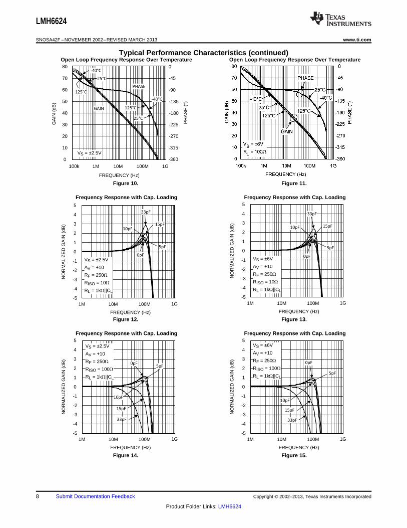
Typical Performance Characteristics (continued)Open Loop Frequency Response Over Temperature Open Loop Frequency Response Over Temperature
Figure 10. Figure 11.
Frequency Response with Cap. Loading Frequency Response with Cap. Loading
Figure 12. Figure 13.
Frequency Response with Cap. Loading Frequency Response with Cap. Loading
Figure 14. Figure 15.
8 Submit Documentation Feedback Copyright © 2002–2013, Texas Instruments Incorporated
Product Folder Links: LMH6624
100k 1M 10M 100M 1G
FREQUENCY (Hz)
-5
-4
-3
-2
-1
0
1
2
3
4
5
NO
RM
ALI
ZE
D G
AIN
(dB
)
VS = ±6V
AV = +20
RF = 500:
VIN = 20mV
VIN = 200mV
100k 1M 10M 100M 1G
FREQUENCY (Hz)
-5
-4
-3
-2
-1
0
1
2
3
4
5
NO
MA
LIZ
ED
GA
IN (
dB)
VS = ±6V
AV = +20
RF = 500:
VIN = 200mV
VIN = 20mV
100k 1M 10M 100M 1G
FREQUENCY (Hz)
-5
-4
-3
-2
-1
0
1
2
3
4
5
NO
RM
ALI
ZE
D G
AIN
(dB
)
VS = ±2.5V
AV = +20
RF = 500:
VIN = 20mV
VIN = 200mV
100k 1M 10M 100M 1G
FREQUENCY (Hz)
-5
-4
-3
-2
-1
0
1
2
3
4
5
NO
MA
LIZ
ED
GA
IN (
dB)
VS = ±2.5V
AV = +20
RF = 500:
VIN = 200mV
VIN = 20mV
100k 1M 10M 100M 1G
FREQUENCY (Hz)
-5
-4
-3
-2
-1
0
1
2
3
4
5N
OM
ALI
ZE
D G
AIN
(dB
)VS = ±2.5V
AV = +10
RF = 500:
VIN = 200mV
VIN = 20mV
100k 1M 10M 100M 1G
FREQUENCY (Hz)
-5
-4
-3
-2
-1
0
1
2
3
4
5
NO
MA
LIZ
ED
GA
IN (
dB)
VS = ±6V
AV = +10
RF = 500:
VIN = 200mV
VIN = 20mV
LMH6624
www.ti.com SNOSA42F –NOVEMBER 2002–REVISED MARCH 2013
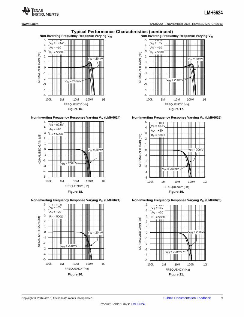
Typical Performance Characteristics (continued)Non-Inverting Frequency Response Varying VIN Non-Inverting Frequency Response Varying VIN
Figure 16. Figure 17.
Non-Inverting Frequency Response Varying VIN (LMH6624) Non-Inverting Frequency Response Varying VIN (LMH6626)
Figure 18. Figure 19.
Non-Inverting Frequency Response Varying VIN (LMH6624) Non-Inverting Frequency Response Varying VIN (LMH6626)
Figure 20. Figure 21.
Copyright © 2002–2013, Texas Instruments Incorporated Submit Documentation Feedback 9
Product Folder Links: LMH6624
4 5 6 7 8 9 10 11 12
VSUPPLY (V)
-300
-250
-200
-150
-100
-50
0
50
VO
S (P
V)
125°C
25°C
-40°C
4 5 6 7 8 9 10 11 12
VSUPPLY (V)
-250
-200
-150
-100
-50
0
50
100
150
VO
S (P
V)
25°C
125°C
-40°C
0 1 2 3 4 50
20
40
60
80
100
120
140
I SO
UR
CE
(m
A)
VOUT (V)
-40°C
25°C
125°C
VS = ±6V
0 1 2 3 4 50
20
40
60
80
100
120
140
160
180
I SO
UR
CE
(m
A)
VOUT (V)
125°C
25°C
-40°C
VS = ±6V
0 0.5 1 1.50
20
40
60
80
100
120
140
I SO
UR
CE
(m
A)
VOUT (V)
-40°C
125°C 25°C
VS = ±2.5V
0 0.5 1 1.50
20
40
60
80
100
120
140
160
I SO
UR
CE
(m
A)
VOUT (V)
125°C25°C
-40°C
VS = ±2.5V
LMH6624
SNOSA42F –NOVEMBER 2002–REVISED MARCH 2013 www.ti.com
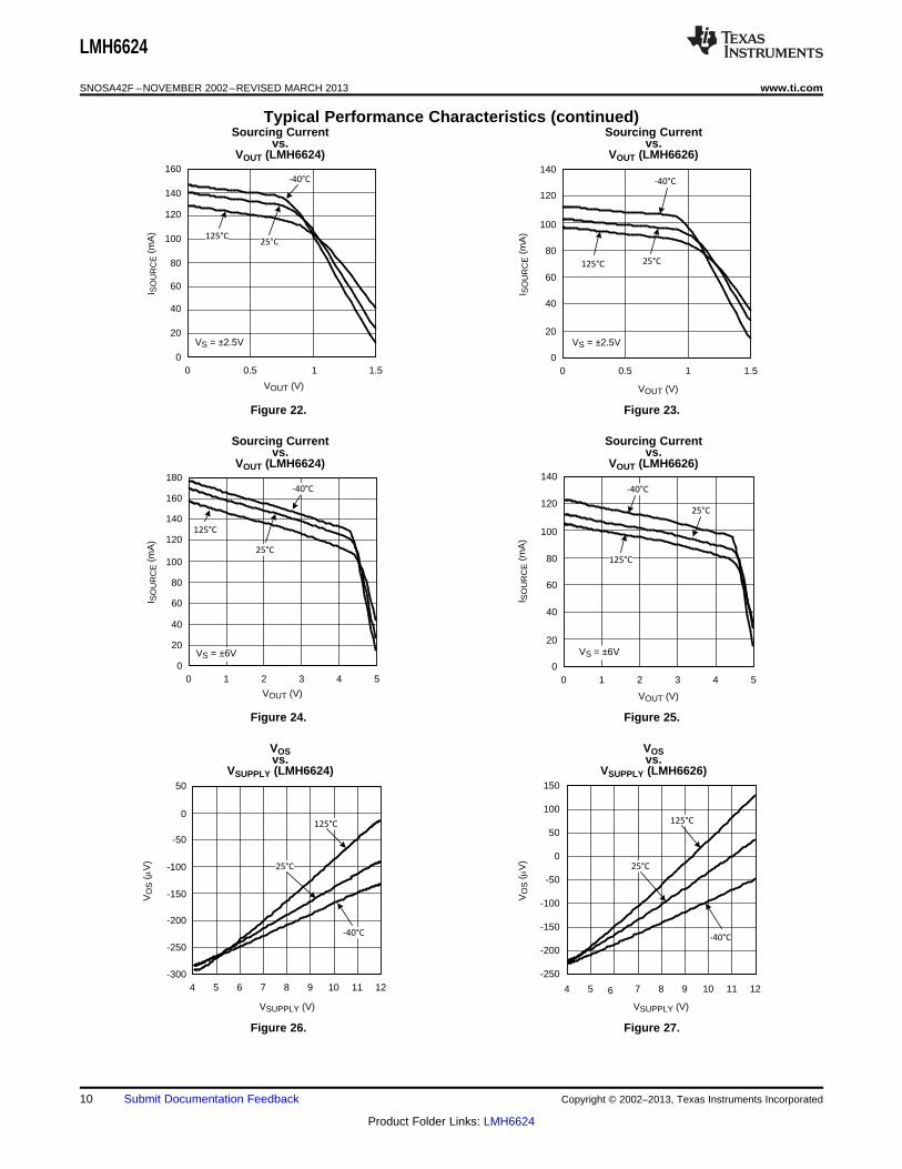
Typical Performance Characteristics (continued)Sourcing Current Sourcing Current
vs. vs.VOUT (LMH6624) VOUT (LMH6626)
Figure 22. Figure 23.
Sourcing Current Sourcing Currentvs. vs.
VOUT (LMH6624) VOUT (LMH6626)
Figure 24. Figure 25.
VOS VOSvs. vs.
VSUPPLY (LMH6624) VSUPPLY (LMH6626)
Figure 26. Figure 27.
10 Submit Documentation Feedback Copyright © 2002–2013, Texas Instruments Incorporated
Product Folder Links: LMH6624
4 5 6 7 8 9 10 11 12
VSUPPLY (V)
-0.15
-0.1
-0.05
0
0.05
0.1
0.15
0.2
I OS
(P
A)
125°C
25°C
-40°C
1k 100k 100M
FREQUENCY (Hz)
-140
-100
-60
0
CR
OS
ST
ALK
(dB
)
10M1M10k
-20
-80
-120
-40
VIN = 60mVPP
AV = +20
RL = 100:
VS = ±6V
VS = ±2.5V
CH 1 OUTPUT
CH 2 OUTPUT
0 1 2 3 4 50
20
40
60
80
100
120
140
I SIN
K (
mA
)
VOUT (V)
-40°C
25°C
125°C
VS = ±6V
0 1 2 3 4 50
20
40
60
80
100
120
140
160
180
I SIN
K (
mA
)
VOUT (V)
125°C
25°C
-40°C
VS = ±6V
0 0.5 1 1.50
20
40
60
80
100
120
140
I SIN
K (
mA
)
VOUT (V)
-40°C
125°C25°C
VS = ±2.5V
0 0.5 1 1.5-20
0
20
40
60
80
100
120
140
160
I SIN
K (
mA
)
VOUT (V)
125°C 25°C
-40°C
VS = ±2.5V
LMH6624
www.ti.com SNOSA42F –NOVEMBER 2002–REVISED MARCH 2013
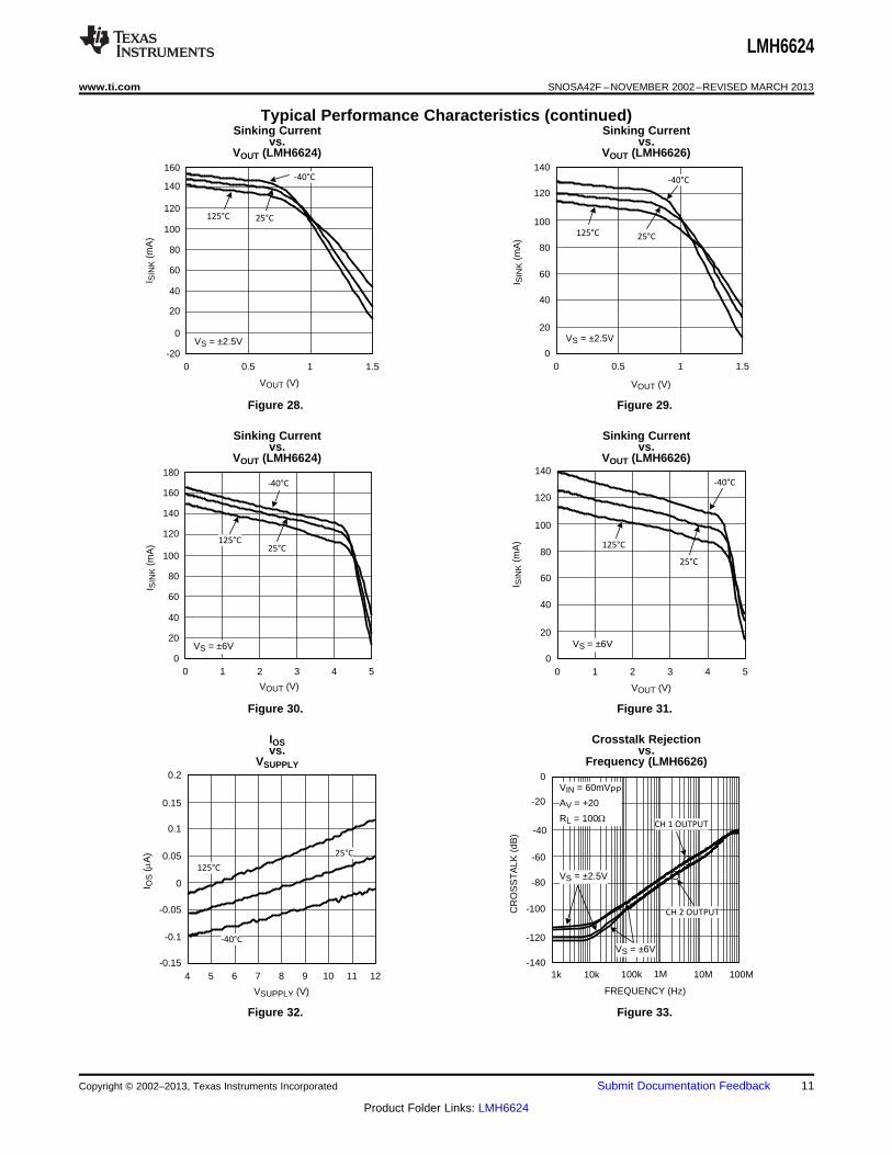
Typical Performance Characteristics (continued)Sinking Current Sinking Current
vs. vs.VOUT (LMH6624) VOUT (LMH6626)
Figure 28. Figure 29.
Sinking Current Sinking Currentvs. vs.
VOUT (LMH6624) VOUT (LMH6626)
Figure 30. Figure 31.
IOS Crosstalk Rejectionvs. vs.
VSUPPLY Frequency (LMH6626)
Figure 32. Figure 33.
Copyright © 2002–2013, Texas Instruments Incorporated Submit Documentation Feedback 11
Product Folder Links: LMH6624
0 2 4 6 8 10 12
VOUT (VPP)
-120
-100
-80
-60
-40
-20
0
DIS
TO
RT
ION
(dB
c)
AV = +20
VS = ±6V
RL = 100:
fC = 10MHz
fC = 1MHz
HD2
HD3
0 0.5 1 1.5 2 2.5 3 3.5 4
VOUT (V)
-120
-100
-80
-60
-40
-20
0
DIS
TO
RT
ION
(dB
c)
AV = +20
VS = ±2.5V
RL = 100:
HD2
HD3
fC = 10MHz
fC = 1MHz
100k 1M 10M 100M
FREQUENCY (Hz)
-140
-120
-100
-80
-60
-40
-20
0
DIS
TO
RT
ION
(dB
c)
AV = +20
RL = 500:
VS = ±2.5V,
VO = 1VPP
VS = ±6V, VO = 2VPP
HD2
HD3
0 20 40 60 80 100-100
-90
-80
-70
-60
-50
DIS
TO
RT
ION
(dB
c)
GAIN (V/V)
fC = 1MHz
RL = 100:
VS = ±6V
VO = 2VPP
HD2
HD3
VS = ±2.5V
VO = 1VPP
100k 1M 10M 100M
FREQUENCY (Hz)
-140
-120
-100
-80
-60
-40
-20
0
DIS
TO
RT
ION
(dB
c)
HD3
HD2
AV = +10
RL = 100:
VS = ±6V, VO = 2VPP
VS = ±2.5V, VO = 1VPP
100k 1M 10M 100M
FREQUENCY (Hz)
-120
-100
-80
-60
-40
-20
0
DIS
TO
RT
ION
(dB
c)
AV = +20
RL = 100:
VS = ±6V,
VO = 2VPP
VS = ±2.5V,
VO = 1VPP
HD2
HD3
LMH6624
SNOSA42F –NOVEMBER 2002–REVISED MARCH 2013 www.ti.com
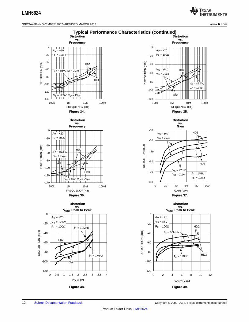
Typical Performance Characteristics (continued)Distortion Distortion
vs. vs.Frequency Frequency
Figure 34. Figure 35.
Distortion Distortionvs. vs.
Frequency Gain
Figure 36. Figure 37.
Distortion Distortionvs. vs.
VOUT Peak to Peak VOUT Peak to Peak
Figure 38. Figure 39.
12 Submit Documentation Feedback Copyright © 2002–2013, Texas Instruments Incorporated
Product Folder Links: LMH6624
0
1k 100k 10M 1G
FREQUENCY (Hz)
-100
-80
-50
PS
RR
(dB
)
100M1M10k
-10
-20
-60
-70
-90
-40
-30
VS = ±2.5V
+PSRR, AV +20
+PSRR, AV +10
-PSRR, AV +20
-PSRR, AV +10
0
1k 100k 10M 1G
FREQUENCY (Hz)
-140
-100
-60
PS
RR
(dB
)
100M1M10k
-20
-40
-80
-120
VS = ±6V
+PSRR, AV = +20
+PSRR, AV = +10
-PSRR, AV = +20
-PSRR, AV = +10
50 m
V/D
IV
10 ns/DIV
VS = ±2.5V
VO = 200mV
AV = +10
RL = 100:10
0 m
V/D
IV
10 ns/DIV
VS = ±6V
VO = 500mV
AV = +20
RL = 100:
200
mV
/DIV
10 ns/DIV
VS = ±2.5V
VO = 1VPP
AV = +10
RL = 100:
200
mV
/DIV
10 ns/DIV
VS = ±6V
VO = 1VPP
AV = +20
RL = 100:
LMH6624
www.ti.com SNOSA42F –NOVEMBER 2002–REVISED MARCH 2013
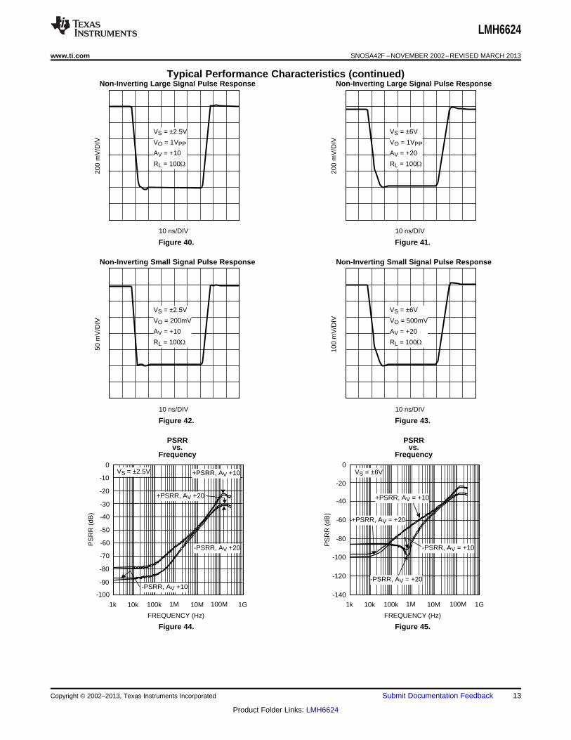
Typical Performance Characteristics (continued)Non-Inverting Large Signal Pulse Response Non-Inverting Large Signal Pulse Response
Figure 40. Figure 41.
Non-Inverting Small Signal Pulse Response Non-Inverting Small Signal Pulse Response
Figure 42. Figure 43.
PSRR PSRRvs. vs.
Frequency Frequency
Figure 44. Figure 45.
Copyright © 2002–2013, Texas Instruments Incorporated Submit Documentation Feedback 13
Product Folder Links: LMH6624
10M 100M 1G
FREQUENCY (Hz)
-5
-4
-3
-2
-1
0
1
2
3
4
5
NO
RM
ALI
ZE
D G
AIN
(dB
)
VS = ±2.5V
AV = +10
RL = 100:
RF = 2k:RF = 1.5k:
RF = 1k:
RF = 511:
RF = 750:
10M 100M 1G
FREQUENCY (Hz)
-5
-4
-3
-2
-1
0
1
2
3
4
5
NO
RM
ALI
ZE
D G
AIN
(dB
)
VS = ±6V
AV = +10V
RL = 100:
RF = 2k:RF = 1.5k:
RF = 1k:
RF = 511:
RF = 750:
1k 100k 100M
FREQUENCY (Hz)
-90
-70
0
CM
RR
(dB
)
10M1M10k
-20
-30
-80
-10
-40
-50
-60
VS = ±2.5V
VIN = 5mVPP
AV = +10
AV = +20
1k 100k 100M
FREQUENCY (Hz)
-90
-70
0
CM
RR
(dB
)
10M1M10k
-20
-30
-80
-10
-40
-50
-60
VS = ±6V
VIN = 5mVPP
AV = +10
AV = +20
LMH6624
SNOSA42F –NOVEMBER 2002–REVISED MARCH 2013 www.ti.com
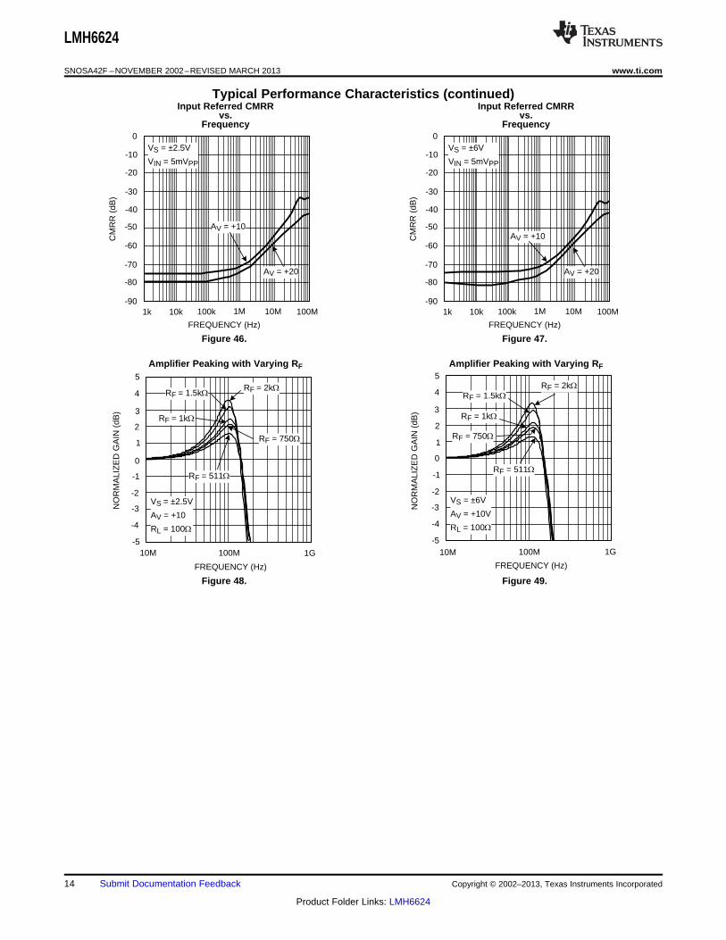
Typical Performance Characteristics (continued)Input Referred CMRR Input Referred CMRR
vs. vs.Frequency Frequency
Figure 46. Figure 47.
Amplifier Peaking with Varying RF Amplifier Peaking with Varying RF
Figure 48. Figure 49.
14 Submit Documentation Feedback Copyright © 2002–2013, Texas Instruments Incorporated
Product Folder Links: LMH6624
LMH6624
www.ti.com SNOSA42F –NOVEMBER 2002–REVISED MARCH 2013
APPLICATION SECTION
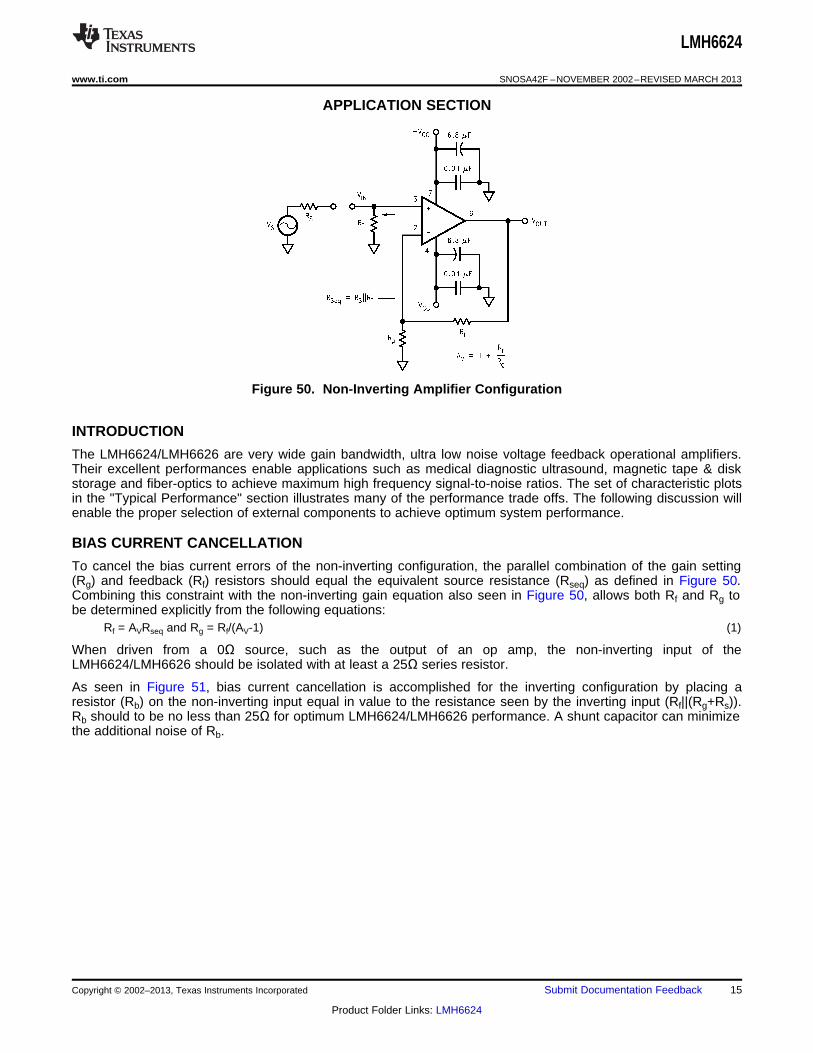
Figure 50. Non-Inverting Amplifier Configuration
INTRODUCTION
The LMH6624/LMH6626 are very wide gain bandwidth, ultra low noise voltage feedback operational amplifiers.Their excellent performances enable applications such as medical diagnostic ultrasound, magnetic tape & diskstorage and fiber-optics to achieve maximum high frequency signal-to-noise ratios. The set of characteristic plotsin the "Typical Performance" section illustrates many of the performance trade offs. The following discussion willenable the proper selection of external components to achieve optimum system performance.
BIAS CURRENT CANCELLATION
To cancel the bias current errors of the non-inverting configuration, the parallel combination of the gain setting(Rg) and feedback (Rf) resistors should equal the equivalent source resistance (Rseq) as defined in Figure 50.Combining this constraint with the non-inverting gain equation also seen in Figure 50, allows both Rf and Rg tobe determined explicitly from the following equations:
Rf = AVRseq and Rg = Rf/(AV-1) (1)
When driven from a 0Ω source, such as the output of an op amp, the non-inverting input of theLMH6624/LMH6626 should be isolated with at least a 25Ω series resistor.
As seen in Figure 51, bias current cancellation is accomplished for the inverting configuration by placing aresistor (Rb) on the non-inverting input equal in value to the resistance seen by the inverting input (Rf||(Rg+Rs)).Rb should to be no less than 25Ω for optimum LMH6624/LMH6626 performance. A shunt capacitor can minimizethe additional noise of Rb.
Copyright © 2002–2013, Texas Instruments Incorporated Submit Documentation Feedback 15
Product Folder Links: LMH6624

LMH6624
SNOSA42F –NOVEMBER 2002–REVISED MARCH 2013 www.ti.com
Figure 51. Inverting Amplifier Configuration
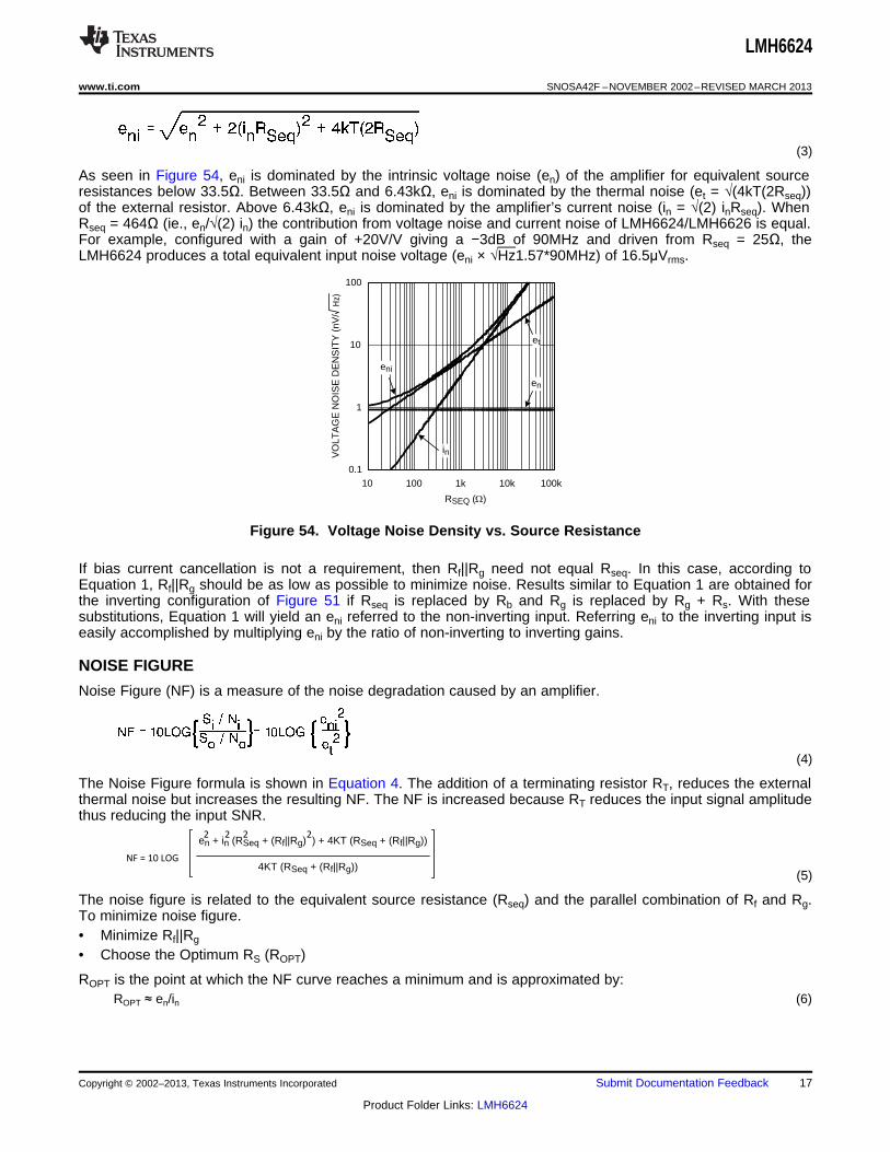
TOTAL INPUT NOISE vs. SOURCE RESISTANCE
To determine maximum signal-to-noise ratios from the LMH6624/LMH6626, an understanding of the interactionbetween the amplifier’s intrinsic noise sources and the noise arising from its external resistors is necessary.
Figure 52 describes the noise model for the non-inverting amplifier configuration showing all noise sources. Inaddition to the intrinsic input voltage noise (en) and current noise (in = in
+ = in−) source, there is also thermal
voltage noise (et = √(4KTR)) associated with each of the external resistors. Equation 1 provides the general formfor total equivalent input voltage noise density (eni). Equation 2 is a simplification of Equation 1 that assumes
Figure 52. Non-Inverting Amplifier Noise Model
(2)
Rf||Rg = Rseq for bias current cancellation. Figure 53 illustrates the equivalent noise model using this assumption.Figure 54 is a plot of eni against equivalent source resistance (Rseq) with all of the contributing voltage noisesource of Equation 2. This plot gives the expected eni for a given (Rseq) which assumes Rf||Rg = Rseq for biascurrent cancellation. The total equivalent output voltage noise (eno) is eni*AV.
Figure 53. Noise Model with Rf||Rg = Rseq
16 Submit Documentation Feedback Copyright © 2002–2013, Texas Instruments Incorporated
Product Folder Links: LMH6624
NF = 10 LOG
en + in (RSeq + (Rf||Rg) ) + 4KT (RSeq + (Rf||Rg)) 2
4KT (RSeq + (Rf||Rg))
2 2 2
10 100 1k 10k 100k
RSEQ (:)
0.1
1
10
100
VO
LTA
GE
NO
ISE
DE
NS
ITY
(nV
/Hz)
eni
en
et
in
LMH6624
www.ti.com SNOSA42F –NOVEMBER 2002–REVISED MARCH 2013
(3)
As seen in Figure 54, eni is dominated by the intrinsic voltage noise (en) of the amplifier for equivalent sourceresistances below 33.5Ω. Between 33.5Ω and 6.43kΩ, eni is dominated by the thermal noise (et = √(4kT(2Rseq))of the external resistor. Above 6.43kΩ, eni is dominated by the amplifier’s current noise (in = √(2) inRseq). WhenRseq = 464Ω (ie., en/√(2) in) the contribution from voltage noise and current noise of LMH6624/LMH6626 is equal.For example, configured with a gain of +20V/V giving a −3dB of 90MHz and driven from Rseq = 25Ω, theLMH6624 produces a total equivalent input noise voltage (eni × √Hz1.57*90MHz) of 16.5μVrms.
Figure 54. Voltage Noise Density vs. Source Resistance
If bias current cancellation is not a requirement, then Rf||Rg need not equal Rseq. In this case, according toEquation 1, Rf||Rg should be as low as possible to minimize noise. Results similar to Equation 1 are obtained forthe inverting configuration of Figure 51 if Rseq is replaced by Rb and Rg is replaced by Rg + Rs. With thesesubstitutions, Equation 1 will yield an eni referred to the non-inverting input. Referring eni to the inverting input iseasily accomplished by multiplying eni by the ratio of non-inverting to inverting gains.
NOISE FIGURE
Noise Figure (NF) is a measure of the noise degradation caused by an amplifier.
(4)
The Noise Figure formula is shown in Equation 4. The addition of a terminating resistor RT, reduces the externalthermal noise but increases the resulting NF. The NF is increased because RT reduces the input signal amplitudethus reducing the input SNR.
(5)
The noise figure is related to the equivalent source resistance (Rseq) and the parallel combination of Rf and Rg.To minimize noise figure.• Minimize Rf||Rg
• Choose the Optimum RS (ROPT)
ROPT is the point at which the NF curve reaches a minimum and is approximated by:ROPT ≈ en/in (6)
Copyright © 2002–2013, Texas Instruments Incorporated Submit Documentation Feedback 17
Product Folder Links: LMH6624
100 1k 10k0
2
4
6
8
10
12
14
16
FEEDBACK RESISTANCE, RF (:)
CU
RR
EN
T N
OIS
E D
EN
SIT
Y (
pA/
Hz)
in
ini
it
en/RF
LMH6624
SNOSA42F –NOVEMBER 2002–REVISED MARCH 2013 www.ti.com
SINGLE SUPPLY OPERATION
The LMH6624/LMH6626 can be operated with single power supply as shown in Figure 55. Both the input andoutput are capacitively coupled to set the DC operating point.
Figure 55. Single Supply Operation
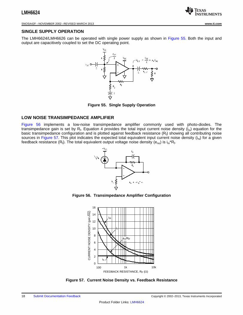
LOW NOISE TRANSIMPEDANCE AMPLIFIER
Figure 56 implements a low-noise transimpedance amplifier commonly used with photo-diodes. Thetransimpedance gain is set by Rf. Equation 4 provides the total input current noise density (ini) equation for thebasic transimpedance configuration and is plotted against feedback resistance (Rf) showing all contributing noisesources in Figure 57. This plot indicates the expected total equivalent input current noise density (ini) for a givenfeedback resistance (Rf). The total equivalent output voltage noise density (eno) is ini*Rf.
Figure 56. Transimpedance Amplifier Configuration
Figure 57. Current Noise Density vs. Feedback Resistance
18 Submit Documentation Feedback Copyright © 2002–2013, Texas Instruments Incorporated
Product Folder Links: LMH6624
C1
+
-
R2R1
C2
RG
RF
RB
RF
C R
RSVO
VIN
-
+
50:50:
RGRF = RB
RG = RS||R
VO #VINKO
sRSC; KO = 1 +
RF
RG
LMH6624
www.ti.com SNOSA42F –NOVEMBER 2002–REVISED MARCH 2013
(7)
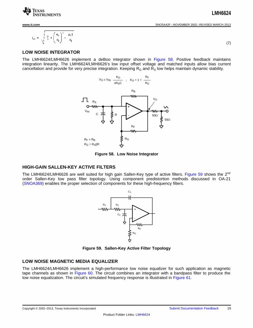
LOW NOISE INTEGRATOR
The LMH6624/LMH6626 implement a deBoo integrator shown in Figure 58. Positive feedback maintainsintegration linearity. The LMH6624/LMH6626’s low input offset voltage and matched inputs allow bias currentcancellation and provide for very precise integration. Keeping RG and RS low helps maintain dynamic stability.
Figure 58. Low Noise Integrator
HIGH-GAIN SALLEN-KEY ACTIVE FILTERS
The LMH6624/LMH6626 are well suited for high gain Sallen-Key type of active filters. Figure 59 shows the 2nd
order Sallen-Key low pass filter topology. Using component predistortion methods discussed in OA-21(SNOA369) enables the proper selection of components for these high-frequency filters.
Figure 59. Sallen-Key Active Filter Topology
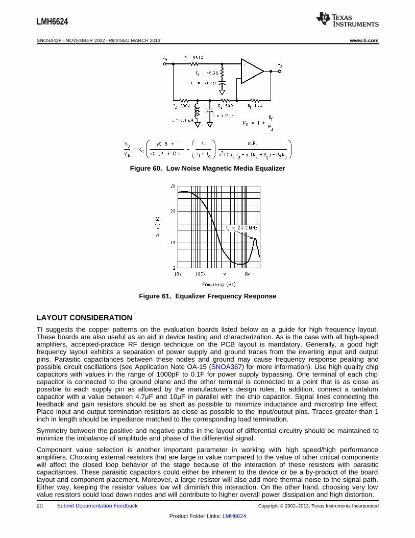
LOW NOISE MAGNETIC MEDIA EQUALIZER
The LMH6624/LMH6626 implement a high-performance low noise equalizer for such application as magnetictape channels as shown in Figure 60. The circuit combines an integrator with a bandpass filter to produce thelow noise equalization. The circuit’s simulated frequency response is illustrated in Figure 61.
Copyright © 2002–2013, Texas Instruments Incorporated Submit Documentation Feedback 19
Product Folder Links: LMH6624
LMH6624
SNOSA42F –NOVEMBER 2002–REVISED MARCH 2013 www.ti.com
Figure 60. Low Noise Magnetic Media Equalizer
Figure 61. Equalizer Frequency Response
LAYOUT CONSIDERATION
TI suggests the copper patterns on the evaluation boards listed below as a guide for high frequency layout.These boards are also useful as an aid in device testing and characterization. As is the case with all high-speedamplifiers, accepted-practice RF design technique on the PCB layout is mandatory. Generally, a good highfrequency layout exhibits a separation of power supply and ground traces from the inverting input and outputpins. Parasitic capacitances between these nodes and ground may cause frequency response peaking andpossible circuit oscillations (see Application Note OA-15 (SNOA367) for more information). Use high quality chipcapacitors with values in the range of 1000pF to 0.1F for power supply bypassing. One terminal of each chipcapacitor is connected to the ground plane and the other terminal is connected to a point that is as close aspossible to each supply pin as allowed by the manufacturer’s design rules. In addition, connect a tantalumcapacitor with a value between 4.7μF and 10μF in parallel with the chip capacitor. Signal lines connecting thefeedback and gain resistors should be as short as possible to minimize inductance and microstrip line effect.Place input and output termination resistors as close as possible to the input/output pins. Traces greater than 1inch in length should be impedance matched to the corresponding load termination.
Symmetry between the positive and negative paths in the layout of differential circuitry should be maintained tominimize the imbalance of amplitude and phase of the differential signal.
Component value selection is another important parameter in working with high speed/high performanceamplifiers. Choosing external resistors that are large in value compared to the value of other critical componentswill affect the closed loop behavior of the stage because of the interaction of these resistors with parasiticcapacitances. These parasitic capacitors could either be inherent to the device or be a by-product of the boardlayout and component placement. Moreover, a large resistor will also add more thermal noise to the signal path.Either way, keeping the resistor values low will diminish this interaction. On the other hand, choosing very lowvalue resistors could load down nodes and will contribute to higher overall power dissipation and high distortion.
20 Submit Documentation Feedback Copyright © 2002–2013, Texas Instruments Incorporated
Product Folder Links: LMH6624
LMH6624
www.ti.com SNOSA42F –NOVEMBER 2002–REVISED MARCH 2013
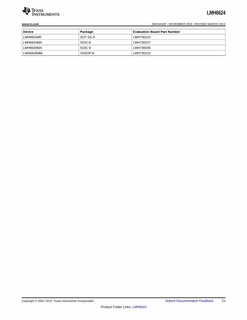
Device Package Evaluation Board Part Number
LMH6624MF SOT-23–5 LMH730216
LMH6624MA SOIC-8 LMH730227
LMH6626MA SOIC-8 LMH730036
LMH6626MM VSSOP-8 LMH730123
Copyright © 2002–2013, Texas Instruments Incorporated Submit Documentation Feedback 21
Product Folder Links: LMH6624
LMH6624
SNOSA42F –NOVEMBER 2002–REVISED MARCH 2013 www.ti.com
REVISION HISTORY
Changes from Revision E (March 2013) to Revision F Page
• Changed layout of National Data Sheet to TI format .......................................................................................................... 20
22 Submit Documentation Feedback Copyright © 2002–2013, Texas Instruments Incorporated
Product Folder Links: LMH6624
PACKAGE OPTION ADDENDUM
www.ti.com 1-Nov-2013
Addendum-Page 1
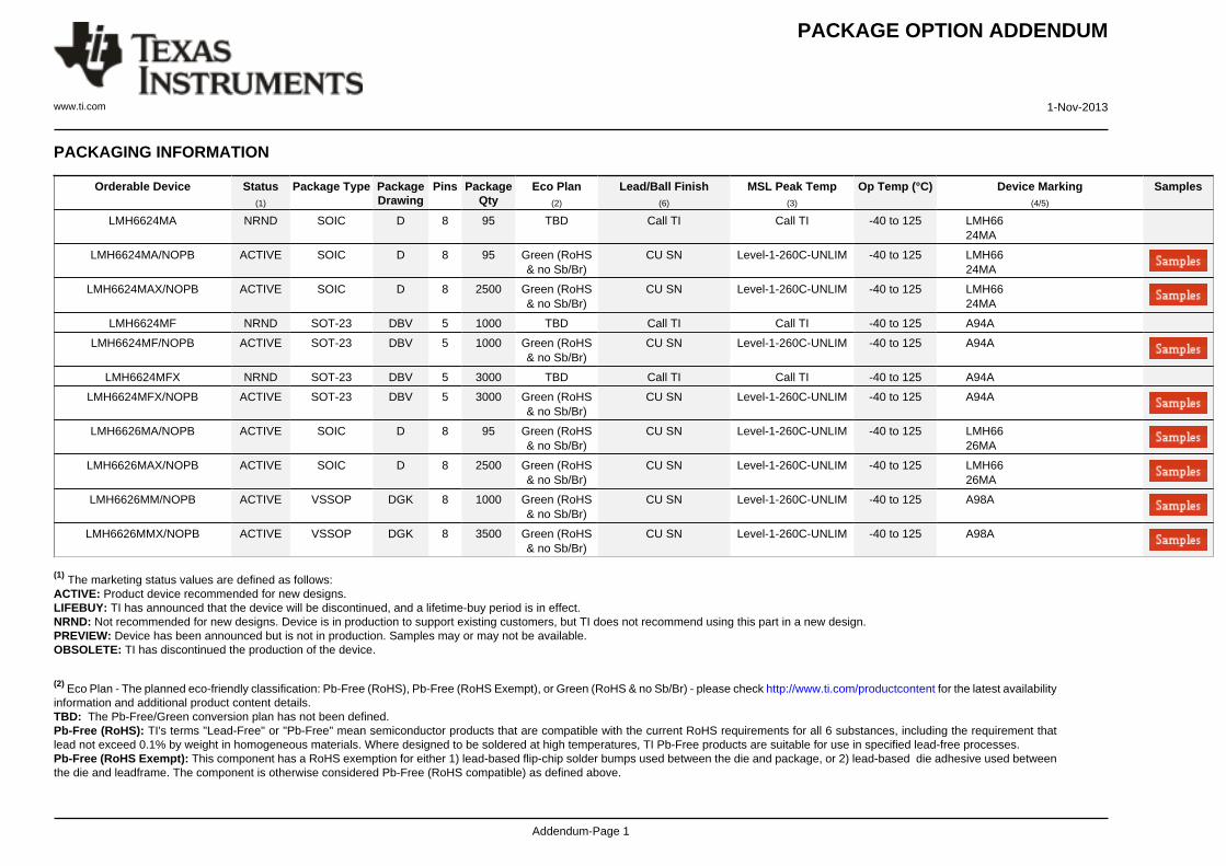
PACKAGING INFORMATION
Orderable Device Status(1)
Package Type PackageDrawing
Pins PackageQty
Eco Plan(2)
Lead/Ball Finish(6)
MSL Peak Temp(3)
Op Temp (°C) Device Marking(4/5)
Samples
LMH6624MA NRND SOIC D 8 95 TBD Call TI Call TI -40 to 125 LMH6624MA
LMH6624MA/NOPB ACTIVE SOIC D 8 95 Green (RoHS& no Sb/Br)
CU SN Level-1-260C-UNLIM -40 to 125 LMH6624MA
LMH6624MAX/NOPB ACTIVE SOIC D 8 2500 Green (RoHS& no Sb/Br)
CU SN Level-1-260C-UNLIM -40 to 125 LMH6624MA
LMH6624MF NRND SOT-23 DBV 5 1000 TBD Call TI Call TI -40 to 125 A94A
LMH6624MF/NOPB ACTIVE SOT-23 DBV 5 1000 Green (RoHS& no Sb/Br)
CU SN Level-1-260C-UNLIM -40 to 125 A94A
LMH6624MFX NRND SOT-23 DBV 5 3000 TBD Call TI Call TI -40 to 125 A94A
LMH6624MFX/NOPB ACTIVE SOT-23 DBV 5 3000 Green (RoHS& no Sb/Br)
CU SN Level-1-260C-UNLIM -40 to 125 A94A
LMH6626MA/NOPB ACTIVE SOIC D 8 95 Green (RoHS& no Sb/Br)
CU SN Level-1-260C-UNLIM -40 to 125 LMH6626MA
LMH6626MAX/NOPB ACTIVE SOIC D 8 2500 Green (RoHS& no Sb/Br)
CU SN Level-1-260C-UNLIM -40 to 125 LMH6626MA
LMH6626MM/NOPB ACTIVE VSSOP DGK 8 1000 Green (RoHS& no Sb/Br)
CU SN Level-1-260C-UNLIM -40 to 125 A98A
LMH6626MMX/NOPB ACTIVE VSSOP DGK 8 3500 Green (RoHS& no Sb/Br)
CU SN Level-1-260C-UNLIM -40 to 125 A98A
(1) The marketing status values are defined as follows:ACTIVE: Product device recommended for new designs.LIFEBUY: TI has announced that the device will be discontinued, and a lifetime-buy period is in effect.NRND: Not recommended for new designs. Device is in production to support existing customers, but TI does not recommend using this part in a new design.PREVIEW: Device has been announced but is not in production. Samples may or may not be available.OBSOLETE: TI has discontinued the production of the device.
(2) Eco Plan - The planned eco-friendly classification: Pb-Free (RoHS), Pb-Free (RoHS Exempt), or Green (RoHS & no Sb/Br) - please check http://www.ti.com/productcontent for the latest availabilityinformation and additional product content details.TBD: The Pb-Free/Green conversion plan has not been defined.Pb-Free (RoHS): TI's terms "Lead-Free" or "Pb-Free" mean semiconductor products that are compatible with the current RoHS requirements for all 6 substances, including the requirement thatlead not exceed 0.1% by weight in homogeneous materials. Where designed to be soldered at high temperatures, TI Pb-Free products are suitable for use in specified lead-free processes.Pb-Free (RoHS Exempt): This component has a RoHS exemption for either 1) lead-based flip-chip solder bumps used between the die and package, or 2) lead-based die adhesive used betweenthe die and leadframe. The component is otherwise considered Pb-Free (RoHS compatible) as defined above.
PACKAGE OPTION ADDENDUM
www.ti.com 1-Nov-2013
Addendum-Page 2
Green (RoHS & no Sb/Br): TI defines "Green" to mean Pb-Free (RoHS compatible), and free of Bromine (Br) and Antimony (Sb) based flame retardants (Br or Sb do not exceed 0.1% by weightin homogeneous material)
(3) MSL, Peak Temp. - The Moisture Sensitivity Level rating according to the JEDEC industry standard classifications, and peak solder temperature.
(4) There may be additional marking, which relates to the logo, the lot trace code information, or the environmental category on the device.
(5) Multiple Device Markings will be inside parentheses. Only one Device Marking contained in parentheses and separated by a "~" will appear on a device. If a line is indented then it is a continuationof the previous line and the two combined represent the entire Device Marking for that device.
(6) Lead/Ball Finish - Orderable Devices may have multiple material finish options. Finish options are separated by a vertical ruled line. Lead/Ball Finish values may wrap to two lines if the finishvalue exceeds the maximum column width.
Important Information and Disclaimer:The information provided on this page represents TI's knowledge and belief as of the date that it is provided. TI bases its knowledge and belief on informationprovided by third parties, and makes no representation or warranty as to the accuracy of such information. Efforts are underway to better integrate information from third parties. TI has taken andcontinues to take reasonable steps to provide representative and accurate information but may not have conducted destructive testing or chemical analysis on incoming materials and chemicals.TI and TI suppliers consider certain information to be proprietary, and thus CAS numbers and other limited information may not be available for release.
In no event shall TI's liability arising out of such information exceed the total purchase price of the TI part(s) at issue in this document sold by TI to Customer on an annual basis.
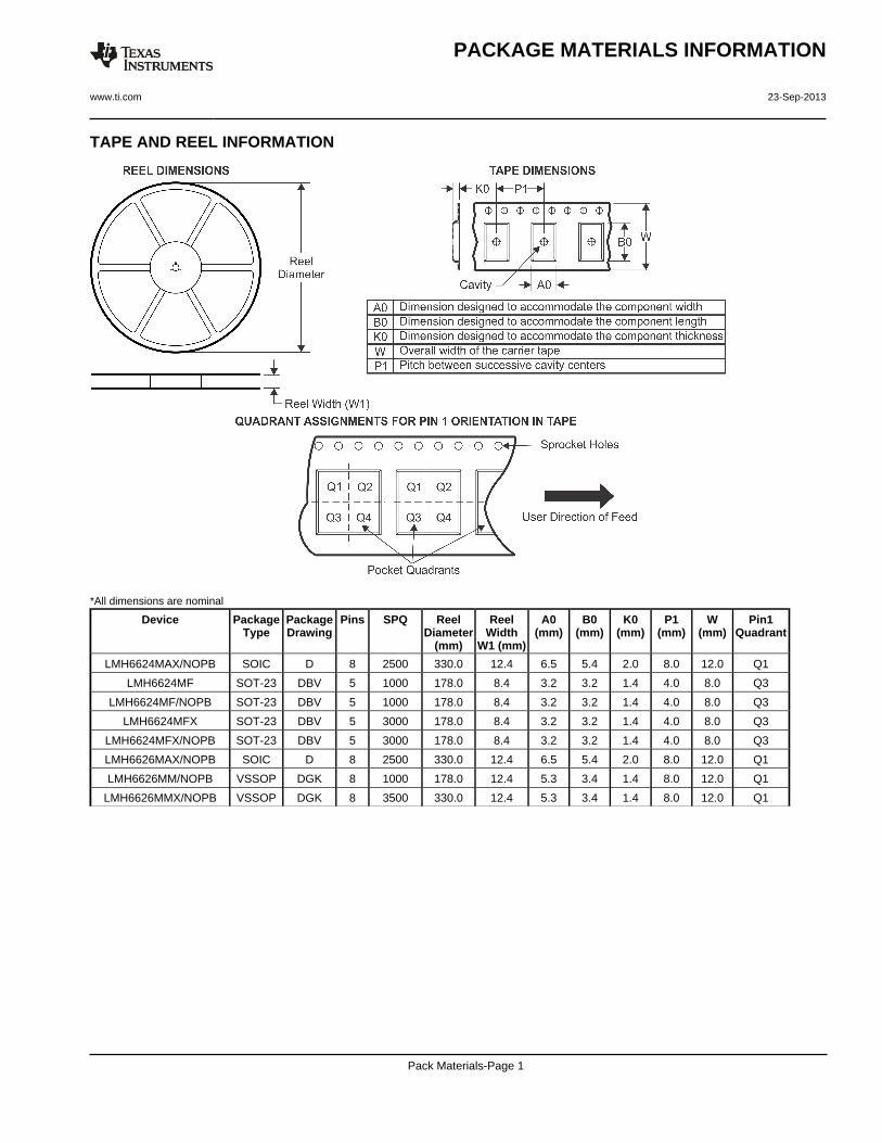
TAPE AND REEL INFORMATION
*All dimensions are nominal
Device PackageType
PackageDrawing
Pins SPQ ReelDiameter
(mm)
ReelWidth
W1 (mm)
A0(mm)
B0(mm)
K0(mm)
P1(mm)
W(mm)
Pin1Quadrant
LMH6624MAX/NOPB SOIC D 8 2500 330.0 12.4 6.5 5.4 2.0 8.0 12.0 Q1
LMH6624MF SOT-23 DBV 5 1000 178.0 8.4 3.2 3.2 1.4 4.0 8.0 Q3
LMH6624MF/NOPB SOT-23 DBV 5 1000 178.0 8.4 3.2 3.2 1.4 4.0 8.0 Q3
LMH6624MFX SOT-23 DBV 5 3000 178.0 8.4 3.2 3.2 1.4 4.0 8.0 Q3
LMH6624MFX/NOPB SOT-23 DBV 5 3000 178.0 8.4 3.2 3.2 1.4 4.0 8.0 Q3
LMH6626MAX/NOPB SOIC D 8 2500 330.0 12.4 6.5 5.4 2.0 8.0 12.0 Q1
LMH6626MM/NOPB VSSOP DGK 8 1000 178.0 12.4 5.3 3.4 1.4 8.0 12.0 Q1
LMH6626MMX/NOPB VSSOP DGK 8 3500 330.0 12.4 5.3 3.4 1.4 8.0 12.0 Q1
PACKAGE MATERIALS INFORMATION
www.ti.com 23-Sep-2013
Pack Materials-Page 1
*All dimensions are nominal
Device Package Type Package Drawing Pins SPQ Length (mm) Width (mm) Height (mm)
LMH6624MAX/NOPB SOIC D 8 2500 367.0 367.0 35.0
LMH6624MF SOT-23 DBV 5 1000 210.0 185.0 35.0
LMH6624MF/NOPB SOT-23 DBV 5 1000 210.0 185.0 35.0
LMH6624MFX SOT-23 DBV 5 3000 210.0 185.0 35.0
LMH6624MFX/NOPB SOT-23 DBV 5 3000 210.0 185.0 35.0
LMH6626MAX/NOPB SOIC D 8 2500 367.0 367.0 35.0
LMH6626MM/NOPB VSSOP DGK 8 1000 210.0 185.0 35.0
LMH6626MMX/NOPB VSSOP DGK 8 3500 367.0 367.0 35.0
PACKAGE MATERIALS INFORMATION
www.ti.com 23-Sep-2013
Pack Materials-Page 2

IMPORTANT NOTICE
Texas Instruments Incorporated and its subsidiaries (TI) reserve the right to make corrections, enhancements, improvements and otherchanges to its semiconductor products and services per JESD46, latest issue, and to discontinue any product or service per JESD48, latestissue. Buyers should obtain the latest relevant information before placing orders and should verify that such information is current andcomplete. All semiconductor products (also referred to herein as “components”) are sold subject to TI’s terms and conditions of salesupplied at the time of order acknowledgment.
TI warrants performance of its components to the specifications applicable at the time of sale, in accordance with the warranty in TI’s termsand conditions of sale of semiconductor products. Testing and other quality control techniques are used to the extent TI deems necessaryto support this warranty. Except where mandated by applicable law, testing of all parameters of each component is not necessarilyperformed.
TI assumes no liability for applications assistance or the design of Buyers’ products. Buyers are responsible for their products andapplications using TI components. To minimize the risks associated with Buyers’ products and applications, Buyers should provideadequate design and operating safeguards.
TI does not warrant or represent that any license, either express or implied, is granted under any patent right, copyright, mask work right, orother intellectual property right relating to any combination, machine, or process in which TI components or services are used. Informationpublished by TI regarding third-party products or services does not constitute a license to use such products or services or a warranty orendorsement thereof. Use of such information may require a license from a third party under the patents or other intellectual property of thethird party, or a license from TI under the patents or other intellectual property of TI.
Reproduction of significant portions of TI information in TI data books or data sheets is permissible only if reproduction is without alterationand is accompanied by all associated warranties, conditions, limitations, and notices. TI is not responsible or liable for such altereddocumentation. Information of third parties may be subject to additional restrictions.
Resale of TI components or services with statements different from or beyond the parameters stated by TI for that component or servicevoids all express and any implied warranties for the associated TI component or service and is an unfair and deceptive business practice.TI is not responsible or liable for any such statements.
Buyer acknowledges and agrees that it is solely responsible for compliance with all legal, regulatory and safety-related requirementsconcerning its products, and any use of TI components in its applications, notwithstanding any applications-related information or supportthat may be provided by TI. Buyer represents and agrees that it has all the necessary expertise to create and implement safeguards whichanticipate dangerous consequences of failures, monitor failures and their consequences, lessen the likelihood of failures that might causeharm and take appropriate remedial actions. Buyer will fully indemnify TI and its representatives against any damages arising out of the useof any TI components in safety-critical applications.
In some cases, TI components may be promoted specifically to facilitate safety-related applications. With such components, TI’s goal is tohelp enable customers to design and create their own end-product solutions that meet applicable functional safety standards andrequirements. Nonetheless, such components are subject to these terms.
No TI components are authorized for use in FDA Class III (or similar life-critical medical equipment) unless authorized officers of the partieshave executed a special agreement specifically governing such use.
Only those TI components which TI has specifically designated as military grade or “enhanced plastic” are designed and intended for use inmilitary/aerospace applications or environments. Buyer acknowledges and agrees that any military or aerospace use of TI componentswhich have not been so designated is solely at the Buyer's risk, and that Buyer is solely responsible for compliance with all legal andregulatory requirements in connection with such use.
TI has specifically designated certain components as meeting ISO/TS16949 requirements, mainly for automotive use. In any case of use ofnon-designated products, TI will not be responsible for any failure to meet ISO/TS16949.
Products Applications
Audio www.ti.com/audio Automotive and Transportation www.ti.com/automotive
Amplifiers amplifier.ti.com Communications and Telecom www.ti.com/communications
Data Converters dataconverter.ti.com Computers and Peripherals www.ti.com/computers
DLP® Products www.dlp.com Consumer Electronics www.ti.com/consumer-apps
DSP dsp.ti.com Energy and Lighting www.ti.com/energy
Clocks and Timers www.ti.com/clocks Industrial www.ti.com/industrial
Interface interface.ti.com Medical www.ti.com/medical
Logic logic.ti.com Security www.ti.com/security
Power Mgmt power.ti.com Space, Avionics and Defense www.ti.com/space-avionics-defense
Microcontrollers microcontroller.ti.com Video and Imaging www.ti.com/video
RFID www.ti-rfid.com
OMAP Applications Processors www.ti.com/omap TI E2E Community e2e.ti.com
Wireless Connectivity www.ti.com/wirelessconnectivity
Mailing Address: Texas Instruments, Post Office Box 655303, Dallas, Texas 75265Copyright © 2013, Texas Instruments Incorporated