Embed Size (px)
Citation preview
AEC+
Equalizer Filter
AEC-
MUTE
MUTEREF
DC Restoration/ Level Control
AutomaticEqualization
Control
SDI
SDI SDO
SDO
BYPASS
OutputDriver
6
Carrier Detect/ Mute
Energy Detect
Energy Detect
CD
Product
Folder
Sample &Buy
Technical
Documents
Tools &
Software
Support &Community
LMH0344SNLS233O –APRIL 2007–REVISED JULY 2015
LMH0344 3-Gbps HD - SD SDI Adaptive Cable Equalizer1 Features 2 Applications1• Compliant With ST 424, ST 292, ST 344, and ST • ST 424, ST 292, ST 344, and ST 259 Serial
259 (1) Digital Interfaces (1)
• Supports DVB-ASI at 270 Mbps • Serial Digital Data Equalization and Reception• Wide Range of Data Rates: 125 Mbps to 2.97 • Data Recovery Equalization
Gbps3 Description• Equalizes up to 120 Meters of Belden 1694A atThe LMH0344 3-Gbps HD – SD SDI Adaptive Cable2.97 Gbps, up to 140 Meters of Belden 1694A atEqualizer is designed to equalize data transmitted1.485 Gbps, or up to 400 Meters of Belden 1694Aover cable (or any media with similar dispersive lossat 270 Mbpscharacteristics). The equalizer operates over a wide• Equalizes up to 120m of Belden 1694A at 2.97 range of data rates from 125 Mbps to 2.97 Gbps and
Gbps With 0.3 UI Maximum Output Jitter supports ST 424, ST 292, ST 344, and ST 259.• Manual Bypass and Output Mute With a The LMH0344 device implements DC restoration toProgrammable Threshold correctly handle pathological data conditions. The• Single-Ended or Differential Input equalizer may be driven in either a single-ended or
differential configuration.• 50-Ω Differential Outputs (Internal 50-Ω Pullups)• Single 3.3-V Supply Operation Additional features include separate carrier detect
and output mute pins which may be tied together to• 280-mW Typical Power Consumptionmute the output when no signal is present. A• 16-Pin WQFN or 25-Ball CS-BGA Package programmable mute reference is provided to mute the
• Industrial Temperature Range: −40°C to +85°C output at a selectable level of signal degradation.• HBM ESD Rating: 8 kV For applications using the 4:4:4:4 10 bits video• WQFN Version Footprint Compatible With the format, the LMH0394 cable equalizer will provide
LMH0044, LMH0384, and LMH0074 better performance.• Replaces the Semtech GS2974A or GS2974B The device is available in two space–saving
packages: a 4-mm × 4-mm 16-pin WQFN and evenmore space-efficient 3-mm × 3-mm 25-ball CS-BGApackage.
Device Information(1)
PART NUMBER PACKAGE BODY SIZE (NOM)(1) Due to SMPTE naming convention, all SMPTE Engineering WQFN (16) 4.00 mm × 4.00 mmDocuments will be numbered as a two-letter prefix and a LMH0344
CS-BGA (25) 3.00 mm × 3.00 mmnumber. Documents and references with the same rootnumber and year are functionally identical; for example ST
(1) For all available packages, see the orderable addendum at424-2006 and SMPTE 424M-2006 refer to the samethe end of the data sheet.document.
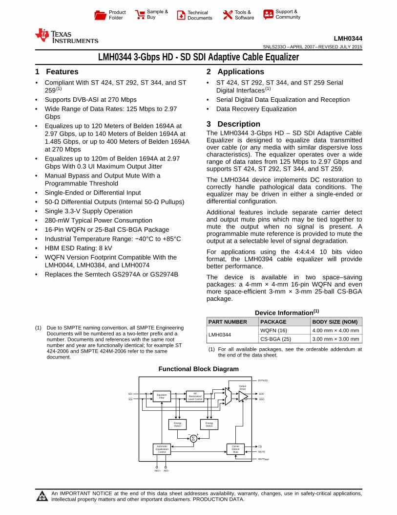
Functional Block Diagram
1
An IMPORTANT NOTICE at the end of this data sheet addresses availability, warranty, changes, use in safety-critical applications,intellectual property matters and other important disclaimers. PRODUCTION DATA.
LMH0344SNLS233O –APRIL 2007–REVISED JULY 2015 www.ti.com
Table of Contents7.4 Device Functional Modes........................................ 101 Features .................................................................. 1
8 Application and Implementation ........................ 112 Applications ........................................................... 18.1 Application Information............................................ 113 Description ............................................................. 18.2 Typical Application ................................................. 114 Revision History..................................................... 28.3 Dos and Don'ts........................................................ 135 Pin Configurations and Functions ....................... 3
9 Power Supply Recommendations ...................... 136 Specifications......................................................... 610 Layout................................................................... 146.1 Absolute Maximum Ratings ...................................... 6
10.1 Layout Guidelines ................................................. 146.2 ESD Ratings.............................................................. 610.2 Layout Example .................................................... 156.3 Recommended Operating Conditions....................... 6
11 Device and Documentation Support ................. 166.4 Thermal Information .................................................. 611.1 Documentation Support ........................................ 166.5 DC Electrical Characteristics .................................... 611.2 Community Resources.......................................... 166.6 AC Electrical Characteristics..................................... 711.3 Trademarks ........................................................... 166.7 Typical Characteristics .............................................. 811.4 Electrostatic Discharge Caution............................ 167 Detailed Description .............................................. 911.5 Glossary ................................................................ 167.1 Overview ................................................................... 9
12 Mechanical, Packaging, and Orderable7.2 Functional Block Diagram ......................................... 9Information ........................................................... 167.3 Feature Description................................................... 9
4 Revision HistoryNOTE: Page numbers for previous revisions may differ from page numbers in the current version.
Changes from Revision N (June 2015) to Revision O Page
• Fixed typo in Features bullet to change "Equalizes up 120m of Belden 1694A" to "Equalizes up to 120m of Belden1694A" ................................................................................................................................................................................... 1
Changes from Revision M (January 2014) to Revision N Page
• Added, updated, or renamed the following sections: Device Information Table, Pin Configuration and Functions;Specifications; Applications and Implementation; Detailed Description; Layout;Device and Documentation Support;Mechanical, Packaging, and Ordering Information ............................................................................................................... 1
• Changed "RGBα data patterns" to "4:4:4:4 10-bit video format" in Description section ........................................................ 1
Changes from Revision L (April 2013) to Revision M Page
• Added BYPASS Sentence...................................................................................................................................................... 3• Added BYPASS Sentence...................................................................................................................................................... 4
Changes from Revision K (April 2013) to Revision L Page
• Changed layout of National Data Sheet to TI format ........................................................................................................... 10
2 Submit Documentation Feedback Copyright © 2007–2015, Texas Instruments Incorporated
Product Folder Links: LMH0344
1
4
3
2
LMH0344
12
9
10
11
85 6 7
1316 15 14
VEE
VEE
SDI
SDI SDO
SDO
VEE
VEE
AE
C+
AE
C-
BY
PA
SS
MU
TE
RE
F
CD
VC
C
VC
C
MU
TE
LMH0344www.ti.com SNLS233O –APRIL 2007–REVISED JULY 2015
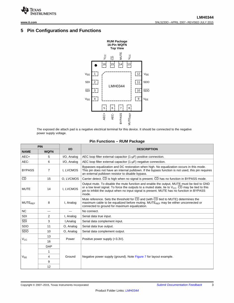
5 Pin Configurations and Functions
RUM Package16-Pin WQFN
Top View
The exposed die attach pad is a negative electrical terminal for this device. It should be connected to the negativepower supply voltage.
Pin Functions – RUM PackagePIN
I/O DESCRIPTIONNAME WQFNAEC+ 5 I/O, Analog AEC loop filter external capacitor (1-µF) positive connection.AEC- 6 I/O, Analog AEC loop filter external capacitor (1-µF) negative connection.
Bypasses equalization and DC restoration when high. No equalization occurs in this mode.BYPASS 7 I, LVCMOS This pin does not have an internal pulldown. If the bypass function is not used, this pin requires
an external pulldown resistor to disable bypass.CD 15 O, LVCMOS Carrier detect. CD is high when no signal is present. CD has no function in BYPASS mode.
Output mute. To disable the mute function and enable the output, MUTE must be tied to GNDor a low level signal. To force the outputs to a muted state, tie to VCC. CD may be tied to thisMUTE 14 I, LVCMOS pin to inhibit the output when no input signal is present. MUTE has no function in BYPASSmode.Mute reference. Sets the threshold for CD and (with CD tied to MUTE) determines the
MUTEREF 8 I, Analog maximum cable to be equalized before muting. MUTEREF may be either unconnected orconnected to ground for maximum equalization.
NC — — No connect.SDI 2 I, Analog Serial data true input.SDI 3 I,Analog Serial data complement input.SDO 11 O, Analog Serial data true output.SDO 10 O, Analog Serial data complement output.
13VCC Power Positive power supply (+3.3V).
16DAP
1VEE 4 Ground Negative power supply (ground). Note Figure 7 for layout example.
912
Copyright © 2007–2015, Texas Instruments Incorporated Submit Documentation Feedback 3
Product Folder Links: LMH0344
VEE
BYPASS
CD
MUTE
E1
D1
C1
B1
A1
VCC
VEE
SDI
NC
E2
D2
C2
B2
A2
VCC
NC
VEE
AEC+
E3
D3
C3
B3
A3
NC
AEC-
VCC
E4
D4
C4
B4
A4
NC
VCC
VEE
NC
MUTEREF
E5
D5
C5
B5
A5
NC
NC
SDO
SDO
A
B
C
D
E
1 2 3 4 5
SDI
LMH0344SNLS233O –APRIL 2007–REVISED JULY 2015 www.ti.com
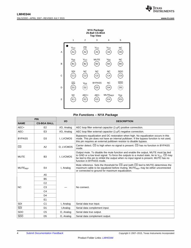
NYA Package25-Ball CS-BGA
Top View
Pin Functions – NYA PackagePIN
I/O DESCRIPTIONNAME CS-BGA BALLAEC+ E2 I/O, Analog AEC loop filter external capacitor (1-µF) positive connection.AEC- E3 I/O, Analog AEC loop filter external capacitor (1-µF) negative connection.
Bypasses equalization and DC restoration when high. No equalization occurs in thisBYPASS D3 I, LVCMOS mode. This pin does not have an internal pulldown. If the bypass function is not used,
this pin requires an external pulldown resistor to disable bypass.Carrier detect. CD is high when no signal is present. CD has no function in BYPASSCD A2 O, LVCMOS mode.Output mute. To disable the mute function and enable the output, MUTE must be tiedto GND or a low level signal. To force the outputs to a muted state, tie to VCC. CD mayMUTE B3 I, LVCMOS be tied to this pin to inhibit the output when no input signal is present. MUTE has nofunction in BYPASS mode.Mute reference. Sets the threshold for CD and (with CD tied to MUTE) determines the
MUTEREF E4 I, Analog maximum cable to be equalized before muting. MUTEREF may be either unconnectedor connected to ground for maximum equalization.
A5B5C2
NC C3 — No connect.C4D4E1
SDI C1 I, Analog Serial data true input.SDI D1 I,Analog Serial data complement input.SDO C5 O, Analog Serial data true output.SDO D5 O, Analog Serial data complement output.
4 Submit Documentation Feedback Copyright © 2007–2015, Texas Instruments Incorporated
Product Folder Links: LMH0344
LMH0344www.ti.com SNLS233O –APRIL 2007–REVISED JULY 2015
Pin Functions – NYA Package (continued)PIN
I/O DESCRIPTIONNAME CS-BGA BALL
A1A3
VCC Power Positive power supply (+3.3V).A4B2B1B4
VEE Ground Negative power supply (ground).D2E5
Copyright © 2007–2015, Texas Instruments Incorporated Submit Documentation Feedback 5
Product Folder Links: LMH0344
LMH0344SNLS233O –APRIL 2007–REVISED JULY 2015 www.ti.com
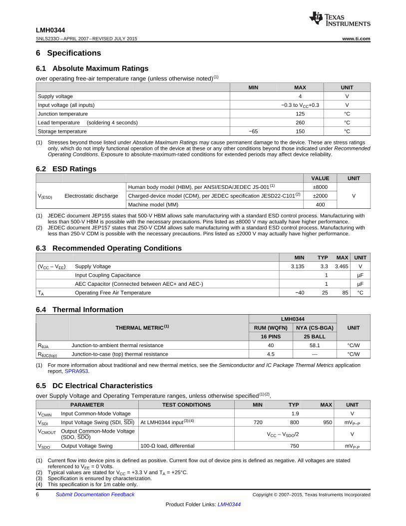
6 Specifications
6.1 Absolute Maximum Ratingsover operating free-air temperature range (unless otherwise noted) (1)
MIN MAX UNITSupply voltage 4 VInput voltage (all inputs) −0.3 to VCC+0.3 VJunction temperature 125 °CLead temperature (soldering 4 seconds) 260 °CStorage temperature −65 150 °C
(1) Stresses beyond those listed under Absolute Maximum Ratings may cause permanent damage to the device. These are stress ratingsonly, which do not imply functional operation of the device at these or any other conditions beyond those indicated under RecommendedOperating Conditions. Exposure to absolute-maximum-rated conditions for extended periods may affect device reliability.
6.2 ESD RatingsVALUE UNIT
Human body model (HBM), per ANSI/ESDA/JEDEC JS-001 (1) ±8000V(ESD) Electrostatic discharge Charged-device model (CDM), per JEDEC specification JESD22-C101 (2) ±2000 V
Machine model (MM) 400
(1) JEDEC document JEP155 states that 500-V HBM allows safe manufacturing with a standard ESD control process. Manufacturing withless than 500-V HBM is possible with the necessary precautions. Pins listed as ±8000 V may actually have higher performance.
(2) JEDEC document JEP157 states that 250-V CDM allows safe manufacturing with a standard ESD control process. Manufacturing withless than 250-V CDM is possible with the necessary precautions. Pins listed as ±2000 V may actually have higher performance.
6.3 Recommended Operating ConditionsMIN TYP MAX UNIT
(VCC – VEE) Supply Voltage 3.135 3.3 3.465 VInput Coupling Capacitance 1 µFAEC Capacitor (Connected between AEC+ and AEC-) 1 µF
TA Operating Free Air Temperature −40 25 85 °C
6.4 Thermal InformationLMH0344
THERMAL METRIC (1) RUM (WQFN) NYA (CS-BGA) UNIT16 PINS 25 BALL
RθJA Junction-to-ambient thermal resistance 40 58.1 °C/WRθJC(top) Junction-to-case (top) thermal resistance 4.5 — °C/W
(1) For more information about traditional and new thermal metrics, see the Semiconductor and IC Package Thermal Metrics applicationreport, SPRA953.
6.5 DC Electrical Characteristicsover Supply Voltage and Operating Temperature ranges, unless otherwise specified (1) (2).
PARAMETER TEST CONDITIONS MIN TYP MAX UNITVCMIN Input Common-Mode Voltage 1.9 VVSDI Input Voltage Swing (SDI, SDI) At LMH0344 input (3) (4) 720 800 950 mVP−P
VCMOUT Output Common-Mode Voltage VCC – VSDO/2 V(SDO, SDO)VSDO Output Voltage Swing 100-Ω load, differential 750 mVP-P
(1) Current flow into device pins is defined as positive. Current flow out of device pins is defined as negative. All voltages are statedreferenced to VEE = 0 Volts.
(2) Typical values are stated for VCC = +3.3 V and TA = +25°C.(3) Specification is ensured by characterization.(4) This specification is for 1m cable only.
6 Submit Documentation Feedback Copyright © 2007–2015, Texas Instruments Incorporated
Product Folder Links: LMH0344
LMH0344www.ti.com SNLS233O –APRIL 2007–REVISED JULY 2015
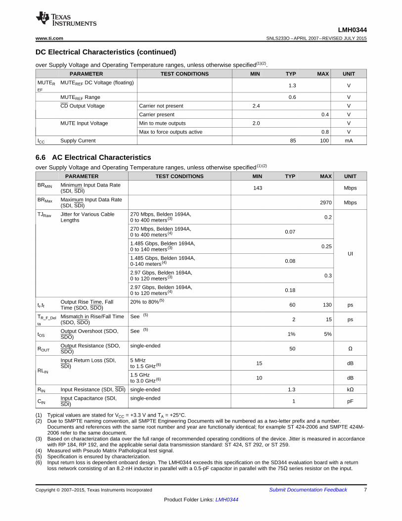
DC Electrical Characteristics (continued)over Supply Voltage and Operating Temperature ranges, unless otherwise specified(1)(2).
PARAMETER TEST CONDITIONS MIN TYP MAX UNITMUTER MUTEREF DC Voltage (floating) 1.3 VEF
MUTEREF Range 0.6 VCD Output Voltage Carrier not present 2.4 V
Carrier present 0.4 VMUTE Input Voltage Min to mute outputs 2.0 V
Max to force outputs active 0.8 VICC Supply Current 85 100 mA
6.6 AC Electrical Characteristicsover Supply Voltage and Operating Temperature ranges, unless otherwise specified (1) (2)
PARAMETER TEST CONDITIONS MIN TYP MAX UNITBRMIN Minimum Input Data Rate 143 Mbps(SDI, SDI)BRMax Maximum Input Data Rate 2970 Mbps(SDI, SDI)TJRaw Jitter for Various Cable 270 Mbps, Belden 1694A, 0.2Lengths 0 to 400 meters (3)
270 Mbps, Belden 1694A, 0.070 to 400 meters (4)
1.485 Gbps, Belden 1694A, 0.250 to 140 meters (3)UI
1.485 Gbps, Belden 1694A, 0.080-140 meters (4)
2.97 Gbps, Belden 1694A, 0.30 to 120 meters (3)
2.97 Gbps, Belden 1694A, 0.180 to 120 meters (4)
Output Rise Time, Fall 20% to 80% (5)tr,tf 60 130 psTime (SDO, SDO)TR_F_Del Mismatch in Rise/Fall Time See (5)
2 15 psta (SDO, SDO)
Output Overshoot (SDO, See (5)tOS 1% 5%SDO)
Output Resistance (SDO, single-endedROUT 50 ΩSDO)Input Return Loss (SDI, 5 MHz 15 dBSDI) to 1.5 GHz (6)
RLIN 1.5 GHz 10 dBto 3.0 GHz (6)
RIN Input Resistance (SDI, SDI) single-ended 1.3 kΩInput Capacitance (SDI, single-endedCIN 1 pFSDI)
(1) Typical values are stated for VCC = +3.3 V and TA = +25°C.(2) Due to SMPTE naming convention, all SMPTE Engineering Documents will be numbered as a two-letter prefix and a number.
Documents and references with the same root number and year are functionally identical; for example ST 424-2006 and SMPTE 424M-2006 refer to the same document.
(3) Based on characterization data over the full range of recommended operating conditions of the device. Jitter is measured in accordancewith RP 184, RP 192, and the applicable serial data transmission standard: ST 424, ST 292, or ST 259.
(4) Measured with Pseudo Matrix Pathological test signal.(5) Specification is ensured by characterization.(6) Input return loss is dependent onboard design. The LMH0344 exceeds this specification on the SD344 evaluation board with a return
loss network consisting of an 8.2-nH inductor in parallel with a 0.5-pF capacitor in parallel with the 75Ω series resistor on the input.
Copyright © 2007–2015, Texas Instruments Incorporated Submit Documentation Feedback 7
Product Folder Links: LMH0344
Time: 56 ps/div
Am
plit
ud
e: 12
5m
V/d
iv
Time: 56 ps/div
Am
plit
ud
e: 12
5m
V/d
iv
LMH0344SNLS233O –APRIL 2007–REVISED JULY 2015 www.ti.com
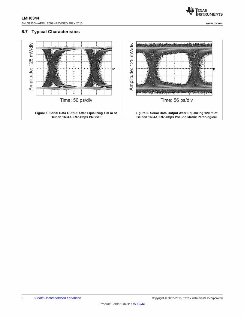
6.7 Typical Characteristics
Figure 1. Serial Data Output After Equalizing 120 m of Figure 2. Serial Data Output After Equalizing 120 m ofBelden 1694A 2.97-Gbps PRBS10 Belden 1694A 2.97-Gbps Pseudo Matrix Pathological
8 Submit Documentation Feedback Copyright © 2007–2015, Texas Instruments Incorporated
Product Folder Links: LMH0344
AEC+
Equalizer Filter
AEC-
MUTE
MUTEREF
DC Restoration/ Level Control
AutomaticEqualization
Control
SDI
SDI SDO
SDO
BYPASS
OutputDriver
6
Carrier Detect/ Mute
Energy Detect
Energy Detect
CD
LMH0344www.ti.com SNLS233O –APRIL 2007–REVISED JULY 2015
7 Detailed Description
7.1 OverviewThe LMH0344 3-Gbps HD–SD SDI Adaptive Cable Equalizer is designed to equalize data transmitted over cableor any other media with similar dispersive loss characteristics. The equalizer operates over a wide range of datarates from 125 Mbps to 2.97 Gbps and supports ST 424, ST 292, ST 344, and ST 259.
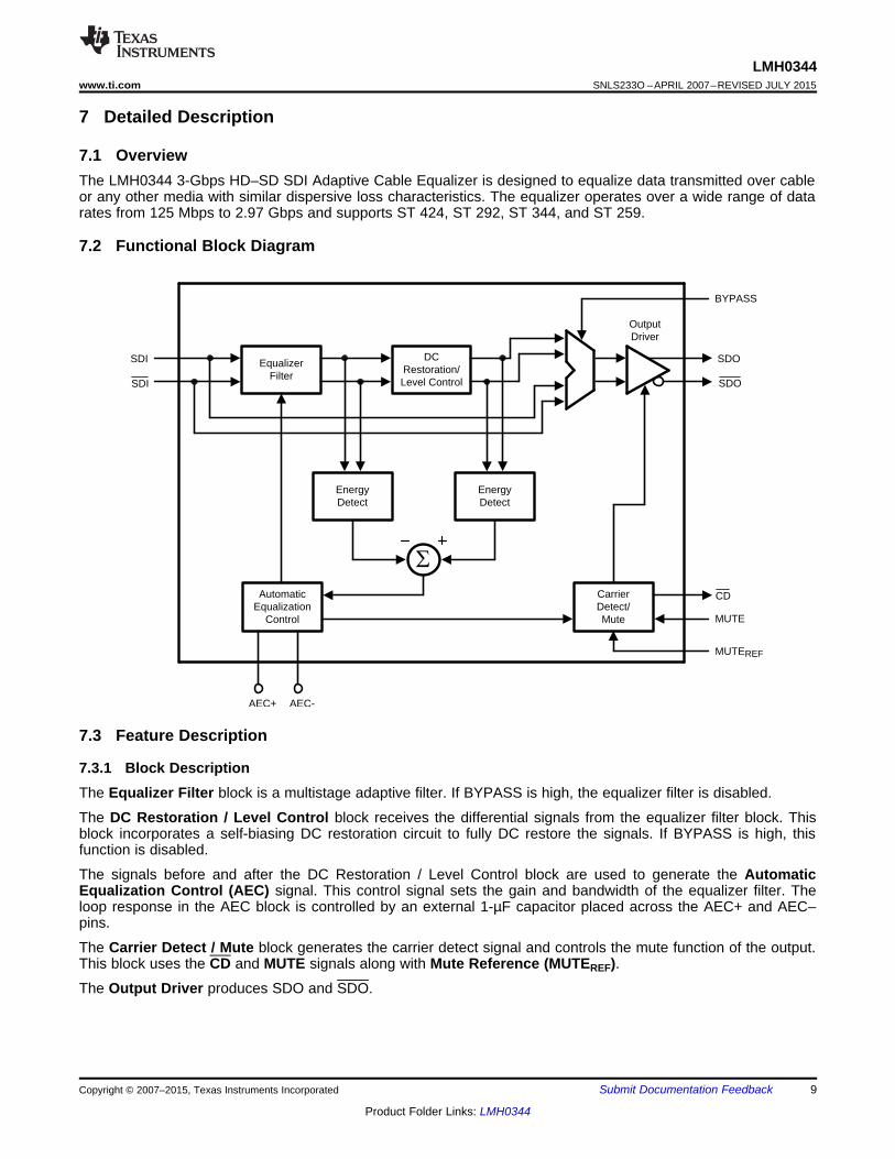
7.2 Functional Block Diagram
7.3 Feature Description
7.3.1 Block DescriptionThe Equalizer Filter block is a multistage adaptive filter. If BYPASS is high, the equalizer filter is disabled.
The DC Restoration / Level Control block receives the differential signals from the equalizer filter block. Thisblock incorporates a self-biasing DC restoration circuit to fully DC restore the signals. If BYPASS is high, thisfunction is disabled.
The signals before and after the DC Restoration / Level Control block are used to generate the AutomaticEqualization Control (AEC) signal. This control signal sets the gain and bandwidth of the equalizer filter. Theloop response in the AEC block is controlled by an external 1-µF capacitor placed across the AEC+ and AEC–pins.
The Carrier Detect / Mute block generates the carrier detect signal and controls the mute function of the output.This block uses the CD and MUTE signals along with Mute Reference (MUTEREF).The Output Driver produces SDO and SDO.
Copyright © 2007–2015, Texas Instruments Incorporated Submit Documentation Feedback 9
Product Folder Links: LMH0344
LMH0344SNLS233O –APRIL 2007–REVISED JULY 2015 www.ti.com
Feature Description (continued)7.3.2 Mute Reference (MuteREF)The mute reference sets the threshold for CD and (with CD tied to MUTE) determines the amount of cable toequalize before automatically muting the outputs. This is set by applying a voltage inversely proportional to thelength of cable to equalize. The applied voltage must be greater than the MUTEREF floating voltage (typically 1.3V) to change the CD threshold. As the applied MUTEREF voltage is increased, the amount of cable that can beequalized before carrier detect is deasserted and the outputs are muted is decreased. MUTEREF may be leftunconnected or connected to ground for maximum equalization before muting.
7.3.3 Carrier Detect (CD) and MuteCarrier detect CD indicates if a valid signal is present at the LMH0344 input. If MUTEREF is used, the carrierdetect threshold will be altered accordingly. CD provides a high voltage when no signal is present at theLMH0344 input. CD is low when a valid input signal is detected.
MUTE can be used to manually mute or enable SDO and SDO. Applying a high input to MUTE will mute theLMH0344 outputs by forcing the output to a logic zero. Applying a low input will force the outputs to be active.
CD and MUTE may be tied together to automatically mute the output when no input signal is present.
7.3.4 Input InterfacingThe LMH0344 accepts either differential or single-ended input. The input must be AC-coupled. Transformercoupling is not supported.
The LMH0344 correctly handles equalizer pathological signals for standard definition and high definition serialdigital video, as described in SMPTE RP 178 and RP 198, respectively.
7.3.5 Output InterfacingThe SDO and SDO outputs are internally loaded with 50 Ω. These outputs produce a 750-mVP-P differentialoutput, or a 375-mVP-P single-ended output.
7.4 Device Functional ModesThe LMH0344 features can be programmed using pin mode only.
10 Submit Documentation Feedback Copyright © 2007–2015, Texas Instruments Incorporated
Product Folder Links: LMH0344
Coaxial Cable
75:
37.4:
75:
3.9 nH 1.0 PF
1.0 PF
LMH0344 3G SDI Adaptive Cable
Equalizer
SDI SDO
SDI SDO
CDMUTEREF
MUTE
BYPASS
RXIN0 TXOUT
RXIN0
LMH0341 3G SDI Deserializer
To FPGARX[4:0]
RXCLK
MUTEREF
MUTE
BYPASS
AE
C+
AE
C-
1.0 PFCD
Reclocked Loopthrough
5-bit LVDS+ clk
TXOUT
LMH0344www.ti.com SNLS233O –APRIL 2007–REVISED JULY 2015
8 Application and Implementation
NOTEInformation in the following applications sections is not part of the TI componentspecification, and TI does not warrant its accuracy or completeness. TI’s customers areresponsible for determining suitability of components for their purposes. Customers shouldvalidate and test their design implementation to confirm system functionality.
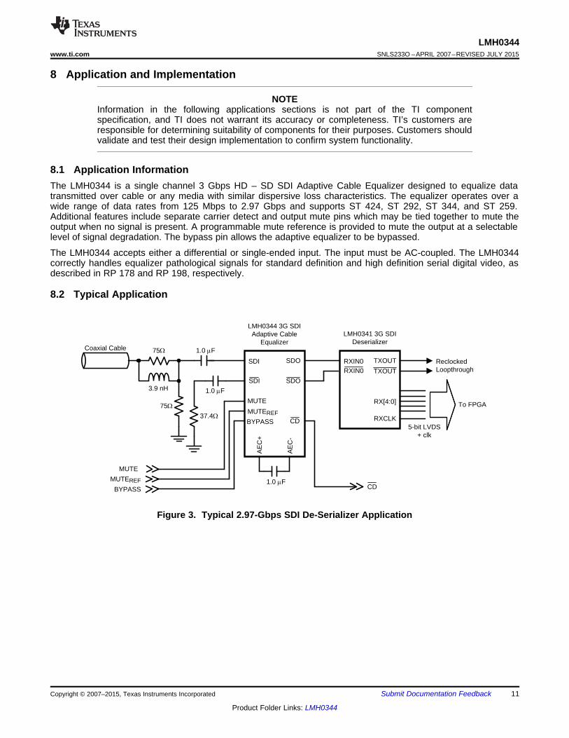
8.1 Application InformationThe LMH0344 is a single channel 3 Gbps HD – SD SDI Adaptive Cable Equalizer designed to equalize datatransmitted over cable or any media with similar dispersive loss characteristics. The equalizer operates over awide range of data rates from 125 Mbps to 2.97 Gbps and supports ST 424, ST 292, ST 344, and ST 259.Additional features include separate carrier detect and output mute pins which may be tied together to mute theoutput when no signal is present. A programmable mute reference is provided to mute the output at a selectablelevel of signal degradation. The bypass pin allows the adaptive equalizer to be bypassed.
The LMH0344 accepts either a differential or single-ended input. The input must be AC-coupled. The LMH0344correctly handles equalizer pathological signals for standard definition and high definition serial digital video, asdescribed in RP 178 and RP 198, respectively.
8.2 Typical Application
Figure 3. Typical 2.97-Gbps SDI De-Serializer Application
Copyright © 2007–2015, Texas Instruments Incorporated Submit Documentation Feedback 11
Product Folder Links: LMH0344
Time: 56 ps /div
Am
plit
ud
e:
12
5 m
V/d
iv
Time: 56 ps /div
Am
plit
ud
e:
12
5 m
V/d
iv
LMH0344SNLS233O –APRIL 2007–REVISED JULY 2015 www.ti.com
Typical Application (continued)8.2.1 Design RequirementsTable 1 lists the design parameters for the LMH0344.
Table 1. LMH0344 Design ParametersDESIGN PARAMETER REQUIREMENT
Required. A common type of AC-coupling capacitor is1 µF ±10% X7R ceramic capacitor (0402 or 0201Input AC-coupling capacitors size). Capacitors may be implemented on the PCB orin the connector.The user should check input common mode voltage ofthe device attached to SDO . If AC-coupling CapacitorOutput AC-coupling capacitors is required, AC-coupling capacitor is expected to be4.7 µF ±10%.Refer to DC Electrical Characteristics and ACInput launch amplitude Electrical Characteristics.
8.2.2 Detailed Design ProcedureTo begin the design process, determine the following:1. Maximum power draw for PCB regulator selection. Use maximum power consumption in the data sheet.2. Closely compare schematic against typical connection diagram in the data sheet.3. Plan out the PCB layout and component placement to minimize parasitic losses and reflections.4. To optimize return loss result, return loss components may need to be adjusted.
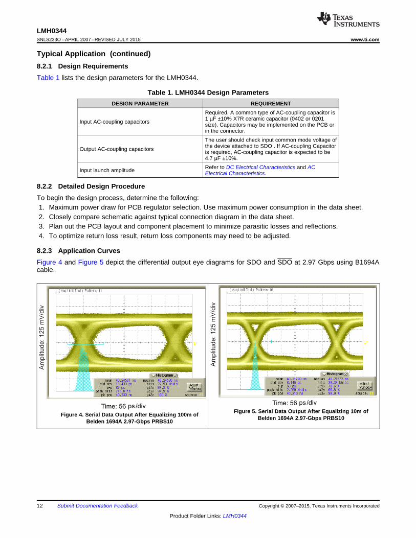
8.2.3 Application CurvesFigure 4 and Figure 5 depict the differential output eye diagrams for SDO and SDO at 2.97 Gbps using B1694Acable.
Figure 5. Serial Data Output After Equalizing 10m ofFigure 4. Serial Data Output After Equalizing 100m of Belden 1694A 2.97-Gbps PRBS10Belden 1694A 2.97-Gbps PRBS10
12 Submit Documentation Feedback Copyright © 2007–2015, Texas Instruments Incorporated
Product Folder Links: LMH0344

LMH0344www.ti.com SNLS233O –APRIL 2007–REVISED JULY 2015
8.3 Dos and Don'tsPay special attention to the PCB layout for the high speed signals. The SMPTE organization specifies therequirements for the Serial Digital Interface to transport digital video at SD, HD, and 3 Gbps data rates overcoaxial cables. One of the requirements is meeting the required Return Loss. This requirement specifies howclosely the port resembles 75-Ω impedance across a specified frequency band. The SMPTE specifications alsodefines the use of AC-coupling capacitors for transporting uncompressed serial data streams with heavy lowfrequency content. This specification requires the use of a 1 µF, AC-coupling capacitors on the input of theLMH0344 to avoid low frequency DC wander.
9 Power Supply RecommendationsFollow these general guidelines when designing the power supply:1. The power supply should be designed to provide the recommended operating conditions in terms of DC
voltage.2. The maximum current draw for the LMH0344 is provided in the data sheet. This figure can be used to
calculate the maximum current the supply must provide.3. The LMH0344 does not require any special power supply filtering, provided the recommended operating
conditions are met. Only standard supply decoupling is required.
Copyright © 2007–2015, Texas Instruments Incorporated Submit Documentation Feedback 13
Product Folder Links: LMH0344
LMH0344SNLS233O –APRIL 2007–REVISED JULY 2015 www.ti.com
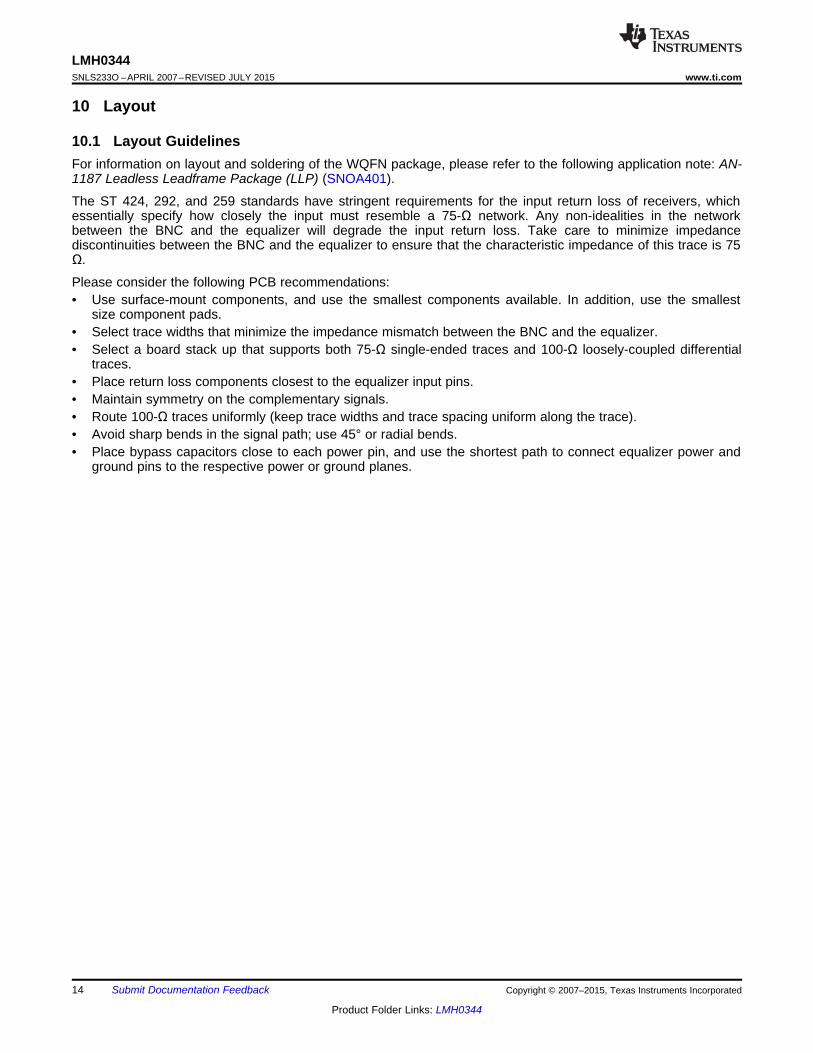
10 Layout
10.1 Layout GuidelinesFor information on layout and soldering of the WQFN package, please refer to the following application note: AN-1187 Leadless Leadframe Package (LLP) (SNOA401).
The ST 424, 292, and 259 standards have stringent requirements for the input return loss of receivers, whichessentially specify how closely the input must resemble a 75-Ω network. Any non-idealities in the networkbetween the BNC and the equalizer will degrade the input return loss. Take care to minimize impedancediscontinuities between the BNC and the equalizer to ensure that the characteristic impedance of this trace is 75Ω.
Please consider the following PCB recommendations:• Use surface-mount components, and use the smallest components available. In addition, use the smallest
size component pads.• Select trace widths that minimize the impedance mismatch between the BNC and the equalizer.• Select a board stack up that supports both 75-Ω single-ended traces and 100-Ω loosely-coupled differential
traces.• Place return loss components closest to the equalizer input pins.• Maintain symmetry on the complementary signals.• Route 100-Ω traces uniformly (keep trace widths and trace spacing uniform along the trace).• Avoid sharp bends in the signal path; use 45° or radial bends.• Place bypass capacitors close to each power pin, and use the shortest path to connect equalizer power and
ground pins to the respective power or ground planes.
14 Submit Documentation Feedback Copyright © 2007–2015, Texas Instruments Incorporated
Product Folder Links: LMH0344
LMH0344www.ti.com SNLS233O –APRIL 2007–REVISED JULY 2015
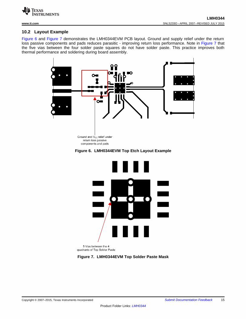
10.2 Layout ExampleFigure 6 and Figure 7 demonstrates the LMH0344EVM PCB layout. Ground and supply relief under the returnloss passive components and pads reduces parasitic - improving return loss performance. Note in Figure 7 thatthe five vias between the four solder paste squares do not have solder paste. This practice improves boththermal performance and soldering during board assembly.
Figure 6. LMH0344EVM Top Etch Layout Example
Figure 7. LMH0344EVM Top Solder Paste Mask
Copyright © 2007–2015, Texas Instruments Incorporated Submit Documentation Feedback 15
Product Folder Links: LMH0344
LMH0344SNLS233O –APRIL 2007–REVISED JULY 2015 www.ti.com
11 Device and Documentation Support
11.1 Documentation Support
11.1.1 Related DocumentationFor additional information, see the following:
Application Note AN- 1187, Leadless Leadframe Package (LLP) (SNOA401).
11.2 Community ResourcesThe following links connect to TI community resources. Linked contents are provided "AS IS" by the respectivecontributors. They do not constitute TI specifications and do not necessarily reflect TI's views; see TI's Terms ofUse.
TI E2E™ Online Community TI's Engineer-to-Engineer (E2E) Community. Created to foster collaborationamong engineers. At e2e.ti.com, you can ask questions, share knowledge, explore ideas and helpsolve problems with fellow engineers.
Design Support TI's Design Support Quickly find helpful E2E forums along with design support tools andcontact information for technical support.
11.3 TrademarksE2E is a trademark of Texas Instruments.All other trademarks are the property of their respective owners.
11.4 Electrostatic Discharge CautionThese devices have limited built-in ESD protection. The leads should be shorted together or the device placed in conductive foamduring storage or handling to prevent electrostatic damage to the MOS gates.
11.5 GlossarySLYZ022 — TI Glossary.
This glossary lists and explains terms, acronyms, and definitions.
12 Mechanical, Packaging, and Orderable InformationThe following pages include mechanical, packaging, and orderable information. This information is the mostcurrent data available for the designated devices. This data is subject to change without notice and revision ofthis document. For browser-based versions of this data sheet, refer to the left-hand navigation.
16 Submit Documentation Feedback Copyright © 2007–2015, Texas Instruments Incorporated
Product Folder Links: LMH0344
PACKAGE OPTION ADDENDUM
www.ti.com 15-Apr-2017
Addendum-Page 1
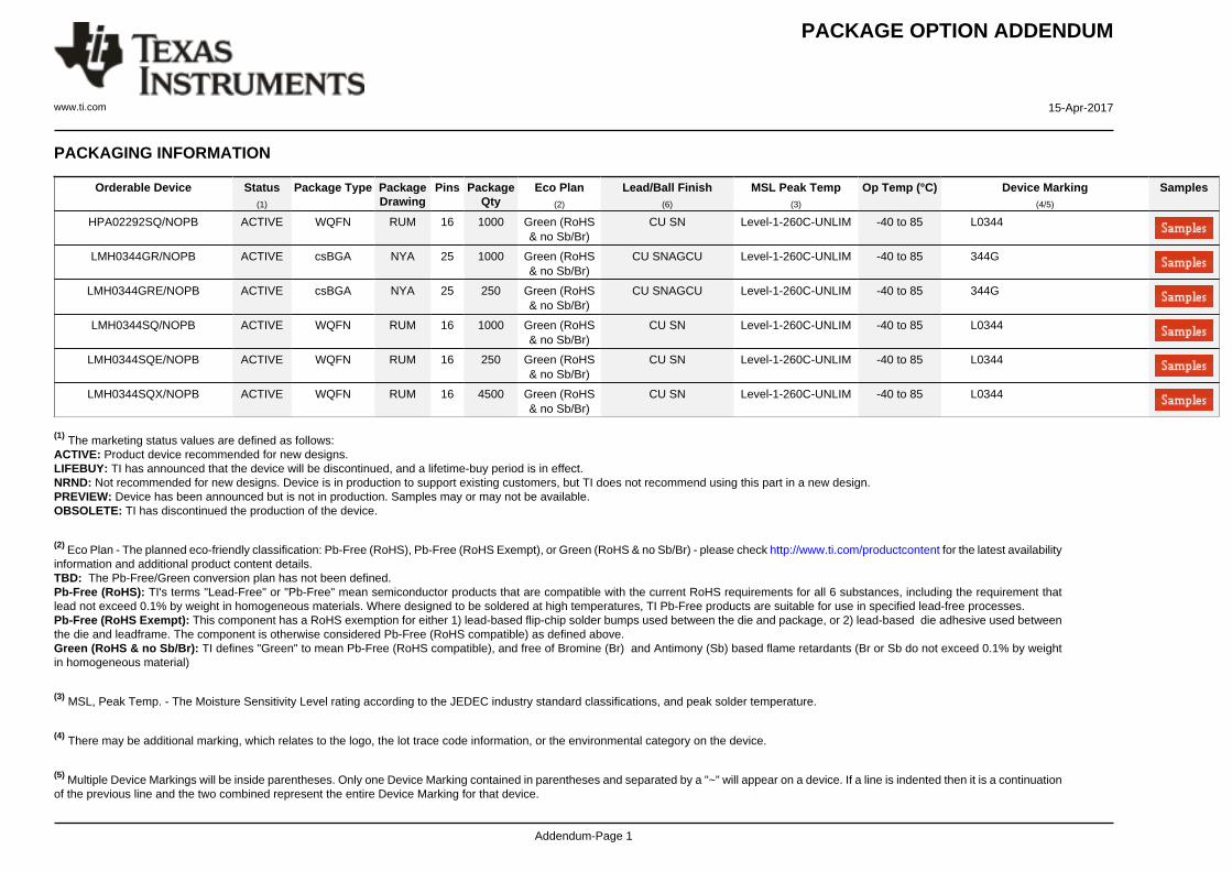
PACKAGING INFORMATION
Orderable Device Status(1)
Package Type PackageDrawing
Pins PackageQty
Eco Plan(2)
Lead/Ball Finish(6)
MSL Peak Temp(3)
Op Temp (°C) Device Marking(4/5)
Samples
HPA02292SQ/NOPB ACTIVE WQFN RUM 16 1000 Green (RoHS& no Sb/Br)
CU SN Level-1-260C-UNLIM -40 to 85 L0344
LMH0344GR/NOPB ACTIVE csBGA NYA 25 1000 Green (RoHS& no Sb/Br)
CU SNAGCU Level-1-260C-UNLIM -40 to 85 344G
LMH0344GRE/NOPB ACTIVE csBGA NYA 25 250 Green (RoHS& no Sb/Br)
CU SNAGCU Level-1-260C-UNLIM -40 to 85 344G
LMH0344SQ/NOPB ACTIVE WQFN RUM 16 1000 Green (RoHS& no Sb/Br)
CU SN Level-1-260C-UNLIM -40 to 85 L0344
LMH0344SQE/NOPB ACTIVE WQFN RUM 16 250 Green (RoHS& no Sb/Br)
CU SN Level-1-260C-UNLIM -40 to 85 L0344
LMH0344SQX/NOPB ACTIVE WQFN RUM 16 4500 Green (RoHS& no Sb/Br)
CU SN Level-1-260C-UNLIM -40 to 85 L0344
(1) The marketing status values are defined as follows:ACTIVE: Product device recommended for new designs.LIFEBUY: TI has announced that the device will be discontinued, and a lifetime-buy period is in effect.NRND: Not recommended for new designs. Device is in production to support existing customers, but TI does not recommend using this part in a new design.PREVIEW: Device has been announced but is not in production. Samples may or may not be available.OBSOLETE: TI has discontinued the production of the device.
(2) Eco Plan - The planned eco-friendly classification: Pb-Free (RoHS), Pb-Free (RoHS Exempt), or Green (RoHS & no Sb/Br) - please check http://www.ti.com/productcontent for the latest availabilityinformation and additional product content details.TBD: The Pb-Free/Green conversion plan has not been defined.Pb-Free (RoHS): TI's terms "Lead-Free" or "Pb-Free" mean semiconductor products that are compatible with the current RoHS requirements for all 6 substances, including the requirement thatlead not exceed 0.1% by weight in homogeneous materials. Where designed to be soldered at high temperatures, TI Pb-Free products are suitable for use in specified lead-free processes.Pb-Free (RoHS Exempt): This component has a RoHS exemption for either 1) lead-based flip-chip solder bumps used between the die and package, or 2) lead-based die adhesive used betweenthe die and leadframe. The component is otherwise considered Pb-Free (RoHS compatible) as defined above.Green (RoHS & no Sb/Br): TI defines "Green" to mean Pb-Free (RoHS compatible), and free of Bromine (Br) and Antimony (Sb) based flame retardants (Br or Sb do not exceed 0.1% by weightin homogeneous material)
(3) MSL, Peak Temp. - The Moisture Sensitivity Level rating according to the JEDEC industry standard classifications, and peak solder temperature.
(4) There may be additional marking, which relates to the logo, the lot trace code information, or the environmental category on the device.
(5) Multiple Device Markings will be inside parentheses. Only one Device Marking contained in parentheses and separated by a "~" will appear on a device. If a line is indented then it is a continuationof the previous line and the two combined represent the entire Device Marking for that device.
PACKAGE OPTION ADDENDUM
www.ti.com 15-Apr-2017
Addendum-Page 2
(6) Lead/Ball Finish - Orderable Devices may have multiple material finish options. Finish options are separated by a vertical ruled line. Lead/Ball Finish values may wrap to two lines if the finishvalue exceeds the maximum column width.
Important Information and Disclaimer:The information provided on this page represents TI's knowledge and belief as of the date that it is provided. TI bases its knowledge and belief on informationprovided by third parties, and makes no representation or warranty as to the accuracy of such information. Efforts are underway to better integrate information from third parties. TI has taken andcontinues to take reasonable steps to provide representative and accurate information but may not have conducted destructive testing or chemical analysis on incoming materials and chemicals.TI and TI suppliers consider certain information to be proprietary, and thus CAS numbers and other limited information may not be available for release.
In no event shall TI's liability arising out of such information exceed the total purchase price of the TI part(s) at issue in this document sold by TI to Customer on an annual basis.
TAPE AND REEL INFORMATION
*All dimensions are nominal
Device PackageType
PackageDrawing
Pins SPQ ReelDiameter
(mm)
ReelWidth
W1 (mm)
A0(mm)
B0(mm)
K0(mm)
P1(mm)
W(mm)
Pin1Quadrant
LMH0344GR/NOPB csBGA NYA 25 1000 178.0 12.4 3.3 3.3 1.6 8.0 12.0 Q1
LMH0344GRE/NOPB csBGA NYA 25 250 178.0 12.4 3.3 3.3 1.6 8.0 12.0 Q1
LMH0344SQ/NOPB WQFN RUM 16 1000 178.0 12.4 4.3 4.3 1.3 8.0 12.0 Q1
LMH0344SQE/NOPB WQFN RUM 16 250 178.0 12.4 4.3 4.3 1.3 8.0 12.0 Q1
LMH0344SQX/NOPB WQFN RUM 16 4500 330.0 12.4 4.3 4.3 1.3 8.0 12.0 Q1
PACKAGE MATERIALS INFORMATION
www.ti.com 2-Sep-2015
Pack Materials-Page 1
*All dimensions are nominal
Device Package Type Package Drawing Pins SPQ Length (mm) Width (mm) Height (mm)
LMH0344GR/NOPB csBGA NYA 25 1000 210.0 185.0 35.0
LMH0344GRE/NOPB csBGA NYA 25 250 210.0 185.0 35.0
LMH0344SQ/NOPB WQFN RUM 16 1000 210.0 185.0 35.0
LMH0344SQE/NOPB WQFN RUM 16 250 210.0 185.0 35.0
LMH0344SQX/NOPB WQFN RUM 16 4500 367.0 367.0 35.0
PACKAGE MATERIALS INFORMATION
www.ti.com 2-Sep-2015
Pack Materials-Page 2
MECHANICAL DATA
NYA0025A
www.ti.com
GRA25A (Rev A)
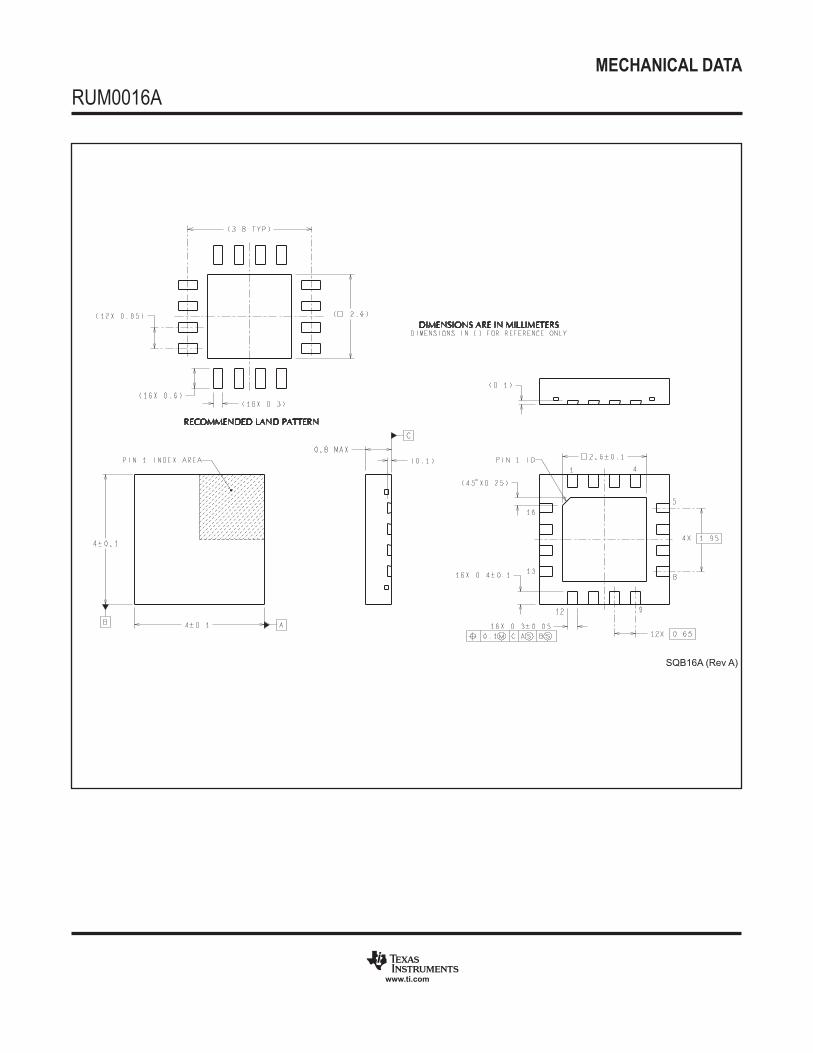
MECHANICAL DATA
RUM0016A
www.ti.com
SQB16A (Rev A)

IMPORTANT NOTICE
Texas Instruments Incorporated (TI) reserves the right to make corrections, enhancements, improvements and other changes to itssemiconductor products and services per JESD46, latest issue, and to discontinue any product or service per JESD48, latest issue. Buyersshould obtain the latest relevant information before placing orders and should verify that such information is current and complete.TI’s published terms of sale for semiconductor products (http://www.ti.com/sc/docs/stdterms.htm) apply to the sale of packaged integratedcircuit products that TI has qualified and released to market. Additional terms may apply to the use or sale of other types of TI products andservices.Reproduction of significant portions of TI information in TI data sheets is permissible only if reproduction is without alteration and isaccompanied by all associated warranties, conditions, limitations, and notices. TI is not responsible or liable for such reproduceddocumentation. Information of third parties may be subject to additional restrictions. Resale of TI products or services with statementsdifferent from or beyond the parameters stated by TI for that product or service voids all express and any implied warranties for theassociated TI product or service and is an unfair and deceptive business practice. TI is not responsible or liable for any such statements.Buyers and others who are developing systems that incorporate TI products (collectively, “Designers”) understand and agree that Designersremain responsible for using their independent analysis, evaluation and judgment in designing their applications and that Designers havefull and exclusive responsibility to assure the safety of Designers' applications and compliance of their applications (and of all TI productsused in or for Designers’ applications) with all applicable regulations, laws and other applicable requirements. Designer represents that, withrespect to their applications, Designer has all the necessary expertise to create and implement safeguards that (1) anticipate dangerousconsequences of failures, (2) monitor failures and their consequences, and (3) lessen the likelihood of failures that might cause harm andtake appropriate actions. Designer agrees that prior to using or distributing any applications that include TI products, Designer willthoroughly test such applications and the functionality of such TI products as used in such applications.TI’s provision of technical, application or other design advice, quality characterization, reliability data or other services or information,including, but not limited to, reference designs and materials relating to evaluation modules, (collectively, “TI Resources”) are intended toassist designers who are developing applications that incorporate TI products; by downloading, accessing or using TI Resources in anyway, Designer (individually or, if Designer is acting on behalf of a company, Designer’s company) agrees to use any particular TI Resourcesolely for this purpose and subject to the terms of this Notice.TI’s provision of TI Resources does not expand or otherwise alter TI’s applicable published warranties or warranty disclaimers for TIproducts, and no additional obligations or liabilities arise from TI providing such TI Resources. TI reserves the right to make corrections,enhancements, improvements and other changes to its TI Resources. TI has not conducted any testing other than that specificallydescribed in the published documentation for a particular TI Resource.Designer is authorized to use, copy and modify any individual TI Resource only in connection with the development of applications thatinclude the TI product(s) identified in such TI Resource. NO OTHER LICENSE, EXPRESS OR IMPLIED, BY ESTOPPEL OR OTHERWISETO ANY OTHER TI INTELLECTUAL PROPERTY RIGHT, AND NO LICENSE TO ANY TECHNOLOGY OR INTELLECTUAL PROPERTYRIGHT OF TI OR ANY THIRD PARTY IS GRANTED HEREIN, including but not limited to any patent right, copyright, mask work right, orother intellectual property right relating to any combination, machine, or process in which TI products or services are used. Informationregarding or referencing third-party products or services does not constitute a license to use such products or services, or a warranty orendorsement thereof. Use of TI Resources may require a license from a third party under the patents or other intellectual property of thethird party, or a license from TI under the patents or other intellectual property of TI.TI RESOURCES ARE PROVIDED “AS IS” AND WITH ALL FAULTS. TI DISCLAIMS ALL OTHER WARRANTIES ORREPRESENTATIONS, EXPRESS OR IMPLIED, REGARDING RESOURCES OR USE THEREOF, INCLUDING BUT NOT LIMITED TOACCURACY OR COMPLETENESS, TITLE, ANY EPIDEMIC FAILURE WARRANTY AND ANY IMPLIED WARRANTIES OFMERCHANTABILITY, FITNESS FOR A PARTICULAR PURPOSE, AND NON-INFRINGEMENT OF ANY THIRD PARTY INTELLECTUALPROPERTY RIGHTS. TI SHALL NOT BE LIABLE FOR AND SHALL NOT DEFEND OR INDEMNIFY DESIGNER AGAINST ANY CLAIM,INCLUDING BUT NOT LIMITED TO ANY INFRINGEMENT CLAIM THAT RELATES TO OR IS BASED ON ANY COMBINATION OFPRODUCTS EVEN IF DESCRIBED IN TI RESOURCES OR OTHERWISE. IN NO EVENT SHALL TI BE LIABLE FOR ANY ACTUAL,DIRECT, SPECIAL, COLLATERAL, INDIRECT, PUNITIVE, INCIDENTAL, CONSEQUENTIAL OR EXEMPLARY DAMAGES INCONNECTION WITH OR ARISING OUT OF TI RESOURCES OR USE THEREOF, AND REGARDLESS OF WHETHER TI HAS BEENADVISED OF THE POSSIBILITY OF SUCH DAMAGES.Unless TI has explicitly designated an individual product as meeting the requirements of a particular industry standard (e.g., ISO/TS 16949and ISO 26262), TI is not responsible for any failure to meet such industry standard requirements.Where TI specifically promotes products as facilitating functional safety or as compliant with industry functional safety standards, suchproducts are intended to help enable customers to design and create their own applications that meet applicable functional safety standardsand requirements. Using products in an application does not by itself establish any safety features in the application. Designers mustensure compliance with safety-related requirements and standards applicable to their applications. Designer may not use any TI products inlife-critical medical equipment unless authorized officers of the parties have executed a special contract specifically governing such use.Life-critical medical equipment is medical equipment where failure of such equipment would cause serious bodily injury or death (e.g., lifesupport, pacemakers, defibrillators, heart pumps, neurostimulators, and implantables). Such equipment includes, without limitation, allmedical devices identified by the U.S. Food and Drug Administration as Class III devices and equivalent classifications outside the U.S.TI may expressly designate certain products as completing a particular qualification (e.g., Q100, Military Grade, or Enhanced Product).Designers agree that it has the necessary expertise to select the product with the appropriate qualification designation for their applicationsand that proper product selection is at Designers’ own risk. Designers are solely responsible for compliance with all legal and regulatoryrequirements in connection with such selection.Designer will fully indemnify TI and its representatives against any damages, costs, losses, and/or liabilities arising out of Designer’s non-compliance with the terms and provisions of this Notice.
Mailing Address: Texas Instruments, Post Office Box 655303, Dallas, Texas 75265Copyright © 2017, Texas Instruments Incorporated