Embed Size (px)
Citation preview

1# Product Family Data Sheet Rev.7.0 2016. 7. 4
Middle Power LED Series 5630
LM561C LM561C is highest performance and lm/W for fluorescent replacement
Features & Benefits
• 0.3 W class middle power LED
• Mold resin for high reliability
• Standard form factor for design flexibility (5.6 × 3.0 mm)

2
Table of Contents
1. Characteristics ----------------------- 3
2. Product Code Information ----------------------- 5
3. Typical Characteristics Graphs ----------------------- 20
4. Outline Drawing & Dimension ----------------------- 23
5. Reliability Test Items & Conditions ----------------------- 24
6. Soldering Conditions ----------------------- 25
7. Tape & Reel ----------------------- 26
8. Label Structure ----------------------- 28
9. Packing Structure ----------------------- 29
10. Precautions in Handling & Use ----------------------- 32

3
1. Characteristics
a) Absolute Maximum Rating
Item Symbol Rating Unit Condition
Ambient / Operating Temperature Ta -40 ~ +85 ºC -
Storage Temperature Tstg -40 ~ +120 ºC -
LED Junction Temperature Tj 110 ºC -
Forward Current IF 200 mA -
Peak Pulsed Forward Current Ifp 300 mA Duty 1/10, pulse width 10 ms
Assembly Process Temperature - 260 <10
ºC s -
ESD (HBM) - ±5 kV -

4
b) Electro-optical Characteristics (IF = 65 mA, Ts = 25 ºC)
Item Unit CRI (Ra)
Min. Nominal CCT (K)
Rank Bin Min. Typ. Max.
Forward Voltage (VF) V XA
AY 2.6 - 2.7
AZ 2.7 - 2.8
A1 2.8 - 2.9
Luminous Flux (Φv) lm 80
2700
S4 30.0 32.0
S5 32.0 34.0
S6 34.0 36.0
3000
S4 30.5 32.5
S5 32.5 34.5
S6 34.5 36.5
3500
S4 31.0 33.0
S5 33.0 35.0
S6 35.0 37.0
4000
S4 32.0 34.0
S5 34.0 36.0
S6 36.0 38.0
5000
S4 33.0 35.0
S5 35.0 37.0
S6 37.0 39.0
5700
S4 32.5 34.5
S5 34.5 36.5
S6 36.5 38.5
6500
S4 32.0 34.0
S5 34.0 36.0
S6 36.0 38.0
Reverse Voltage (@ 5 mA) V 0.7 - 1.2
Color Rendering Index (Ra) - 80 - -
Special CRI (R9) - 0 - -
Thermal Resistance (junction to solder point) ºC/W - 12 16-
Beam Angle º - 120 -
Note:
Samsung maintains measurement tolerance of: forward voltage = ±0.1 V, luminous flux = ±5 %, CRI = ±3, R9 = ±6.5

5
2. Product Code Information
1 2 3 4 5 6 7 8 9 10 11 12 13 14 15 16 17 18
S P M W H T 5 4 1 M L 5 X A R K S 0
Digit PKG Information Code Specification
1 2 3 Samsung Package Middle Power SPM
4 5 Color WH White
6 Product Version T
7 8 9 Form Factor 541 5.6 x 3.0 x 0.7 mm; 4 pads; LM561C
10 Sorting Current (mA) M 65 mA
11 Chromaticity Coordinates L ANSI Standard
12 CRI 5 Min. 80
7 Min. 90
13 14 Forward Voltage (V) XA
XK
2.6~2.9V (2,500 pcs/Reel)
2.6~2.9V (10,000 pcs/Reel)
15 16 CCT (K)
W☆ 2700
Bin Code:
W1, W2, W3, W4, W5, W6, W7, W8, W9, WA, WB, WC, WD, WE, WF, WG
V☆ 3000 V1, V2, V3, V4, V5, V6, V7, V8, V9, VA, VB, VC, VD, VE, VF, VG
U☆ 3500 U1, U2, U3, U4, U5, U6, U7, U8, U9, UA, UB, UC, UD, UE, UF, UG
T☆ 4000 T1, T2, T3, T4, T5, T6, T7, T8, T9, TA, TB, TC, TD, TE, TF, TG
R☆ 5000 R1, R2, R3, R4, R5, R6, R7, R8, R9, RA, RB, RC, RD, RE, RF, RG
Q☆ 5700 Q1, Q2, Q3, Q4, Q5, Q6, Q7, Q8, Q9, QA, QB, QC, QD, QE, QF, QG
P☆ 6500 P1, P2, P3, P4, P5, P6, P7, P8, P9, PA, PB, PC, PD, PE, PF, PG
☆ "0" (Whole bin) "M" (Quarter bin) “K” (K Kitting) or “S” (S Kitting)
17 18 Luminous Flux
S0
S5
S6
Bin Code:
S4, S5, S6
S5
S6

6
a) Luminous Flux Bins(IF = 65 mA, Ts= 25ºC)
CRI (Ra) Min.
Nominal CCT (K)
Product Code Flux Bin Flux Range (Φv, lm)
80
2700 SPMWHT541ML5X◆W☆S0
S4 30.0 ~32.0
S5 32.0 ~34.0
SPMWHT541ML5X◆W☆S5 S5 32.0 ~34.0
3000
SPMWHT541ML5X◆V☆S0
S4 30.5 ~ 32.5
S5 32.5 ~ 34.5
S6 34.5 ~ 36.5
SPMWHT541ML5X◆V☆S5 S5 32.5 ~ 34.5
SPMWHT541ML5X◆V☆S6 S6 34.5 ~ 36.5
3500
SPMWHT541ML5X◆U☆S0
S4 31.0 ~ 33.0
S5 33.0 ~ 35.0
S6 35.0 ~ 37.0
SPMWHT541ML5X◆U☆S5 S5 33.0 ~ 35.0
SPMWHT541ML5X◆U☆S6 S6 35.0 ~ 37.0
4000
SPMWHT541ML5X◆T☆S0
S4 32.0 ~ 34.0
S5 34.0 ~ 36.0
S6 36.0 ~ 38.0
SPMWHT541ML5X◆T☆S5 S5 34.0 ~ 36.0
SPMWHT541ML5X◆T☆S6 S6 36.0 ~ 38.0
5000
SPMWHT541ML5X◆R☆S0
S4 33.0 ~ 35.0
S5 35.0 ~ 37.0
S6 37.0 ~ 39.0
SPMWHT541ML5X◆R☆S5 S5 35.0 ~ 37.0
SPMWHT541ML5X◆R☆S6 S6 37.0 ~ 39.0
5700
SPMWHT541ML5X◆Q☆S0
S4 32.5 ~ 34.5
S5 34.5 ~ 36.5
S6 36.5 ~ 38.5
SPMWHT541ML5X◆Q☆S5 S5 34.5 ~ 36.5
SPMWHT541ML5X◆Q☆S6 S6 36.5 ~ 38.5
6500
SPMWHT541ML5X◆P☆S0
S4 32.0 ~ 34.0
S5 34.0 ~ 36.0
S6 36.0 ~ 38.0
SPMWHT541ML5X◆P☆S5 S5 34.0 ~ 36.0
SPMWHT541ML5X◆P☆S6 S6 36.0 ~ 38.0
Note:
"◆" can be "A" (2,500pcs) or "K" (10,000pcs) of reel taping
"☆" can be "0" (Whole bin), "M" (Quarter bin), "K" (K Kitting) or "S" (S Kitting) of the color binning

7
b) Kitting rule
1) K Kitting bin Concept
1. Under agreement between customer and SAMSUNG ELECTRONICS, SAMSUNG can supply kitting bin (VF, Color, lm).
2. A forward voltage (VF) of kitting bin is combined by a pair of same VF rank such as (A1+A1), (AY+AY) or (AZ+AZ).
3. A Chromaticity Coordinates of kitting bin is mixed by kitting procedure.(below kitting simulation)
4. A luminous flux(lm) of kitting bin is combined by a pair of IV rank such as (S4+S4), (S4+S5) or (S5+S5).
[Kitting example]
※ Each of V,W,X,Y and Z can be one bin without details division.
[Binning Information]
Bin #1 Bin #2
VF
AY AY
AZ AZ
A1 A1
CIE
W (1, 2, 5, 6) Z (B, C, F, G)
V (6, 7, A, B) V (6, 7, A, B)
X (3, 4, 7, 8) Y (9, A, D, E)
IV
S4 S4
S4 S5
S5 S5
S5 S6
S6 S6

8
2) S Kitting bin Concept
1. Under agreement between customer and SAMSUNG ELECTRONICS, SAMSUNG can supply kitting bin (VF, Color, lm).
2. A forward voltage (VF) of kitting bin is combined by a pair of same VF rank such as (A1+A1), (AY+AY) or (AZ+AZ).
3. A Chromaticity Coordinates of kitting bin is mixed by kitting procedure.(below kitting simulation)
4. A luminous flux(lm) of kitting bin is combined by a pair of IV rank such as (S4+S4), (S4+S5) or (S5+S5).
[Kitting example]
※ Each of V,W,X,Y and Z can be one bin without details division.
[Binning Information]
Bin #1 Bin #2 Priority
VF
AY AY
AZ AZ
A1 A1
CIE
W (1, 2, 5) B 1
X (3, 4, 8) A 1
Y (9, D, E) 7 1
Z (C, F, G) 6 1
6 6 2
7 7 2
A A 2
B B 2
V (6, 7, A, B) V (6, 7, A, B) 3
IV
S4 S4
S4 S5
S5 S5
S5 S6
S6 S6
9
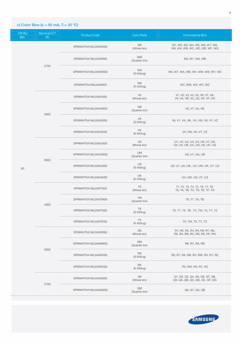
c) Color Bins (IF = 65 mA, Ts= 25 ºC)
CRI (Ra) Min.
Nominal CCT (K)
Product Code Color Rank Chromaticity Bins
80
2700
SPMWHT541ML5XAW0S0 W0 (Whole bin)
W1, W2, W3, W4, W5, W6, W7, W8, W9, WA, WB, WC, WD, WE, WF, WG
SPMWHT541ML5XAWM0 WM (Quarter bin) W6, W7, WA, WB
SPMWHT541ML5XAWSS0 WS (S Kitting) W6, W7, WA, WB, WV, WW, WX, WY, WZ
SPMWHT541ML5XAWK0 WK (K Kitting) WV, WW, WX, WY, WZ
3000
SPMWHT541ML5XAV0S0 V0 (Whole bin)
V1, V2, V3, V4, V5, V6, V7, V8, V9, VA, VB, VC, VD, VE, VF, VG
SPMWHT541ML5XAVMS0 VM (Quarter bin) V6, V7, VA, VB
SPMWHT541ML5XAVSS0 VS (S Kitting) V6, V7, VA, VB , VV, VW, VX, VY, VZ
SPMWHT541ML5XAVKS0 VK (K Kitting) VV, VW, VX, VY, VZ
3500
SPMWHT541ML5XAU0S0 U0 (Whole bin)
U1, U2, U3, U4, U5, U6, U7, U8, U9, UA, UB, UC, UD, UE, UF, UG
SPMWHT541ML5XAUMS0 UM (Quarter bin)
U6, U7, UA, UB
SPMWHT541ML5XAUSS0 US (S Kitting) U6, U7, UA, UB , UV, UW, UX, UY, UZ
SPMWHT541ML5XAUKS0 UK (K Kitting) UV, UW, UX, UY, UZ
4000
SPMWHT541ML5XAT0S0 T0 (Whole bin)
T1, T2, T3, T4, T5, T6, T7, T8, T9, TA, TB, TC, TD, TE, TF, TG
SPMWHT541ML5XATMS0 TM (Quarter bin) T6, T7, TA, TB
SPMWHT541ML5XATSS0 TS (S Kitting)
T6, T7, TA, TB , TV, TW, TX, TY, TZ
SPMWHT541ML5XATKS0 TK (K Kitting) TV, TW, TX, TY, TZ
5000
SPMWHT541ML5XAR0S0 R0 (Whole bin)
R1, R2, R3, R4, R5, R6, R7, R8, R9, RA, RB, RC, RD, RE, RF, RG
SPMWHT541ML5XARMS0 RM (Quarter bin) R6, R7, RA, RB
SPMWHT541ML5XARSS0 RS (S Kitting) R6, R7, RA, RB, RV, RW, RX, RY, RZ
SPMWHT541ML5XARKS0 RK (K Kitting) RV, RW, RX, RY, RZ
5700
SPMWHT541ML5XAQ0S0 Q0 (Whole bin)
Q1, Q2, Q3, Q4, Q5, Q6, Q7, Q8, Q9, QA, QB, QC, QD, QE, QF, QG
SPMWHT541ML5XAQMS0 QM (Quarter bin) Q6, Q7, QA, QB

10
SPMWHT541ML5XAQSS0 QS (S Kitting) Q6, Q7, QA, QB, QV, QW, QX, QY, QZ
SPMWHT541ML5XAQKS0 QK (K Kitting) QV, QW, QX, QY, QZ
6500
SPMWHT541ML5XAP0S0 P0 (Whole bin)
P1, P2, P3, P4, P5, P6, P7, P8, P9, PA, PB, PC, PD, PE, PF, PG
SPMWHT541ML5XAPMS0 PM (Quarter bin) P6, P7, PA, PB
SPMWHT541ML5XAPSS0 PS (S Kitting) P6, P7, PA, PB, PV, PW, PX, PY, PZ
SPMWHT541ML5XAPKS0 PK (K Kitting) PV, PW, PX, PY, PZ

11
d) Voltage Bins (IF = 65 mA, Ts = 25 ºC)
CRI (Ra) Min.
Nominal CCT (K)
Product Code Voltage Rank Voltage Bin Voltage Range
(V)
- - - XA (XK)
AY 2.6 ~ 2.7
AZ 2.7 ~ 2.8
A1 2.8 ~ 2.9

12
e) Chromaticity Region & Coordinates (IF = 65 mA, Ts = 25 ºC)

13
e) Chromaticity Region & Coordinates (IF = 65 mA, Ts = 25 ºC)
Region CIE x CIE y Region CIE x CIE y
W rank (2700 K)
W1
0.4373 0.3893
W9
0.4465 0.4071
0.4418 0.3981 0.4513 0.4164
0.4475 0.3994 0.4573 0.4178
0.4428 0.3906 0.4523 0.4085
W2
0.4428 0.3906
WA
0.4523 0.4085
0.4475 0.3994 0.4573 0.4178
0.4532 0.4008 0.4634 0.4193
0.4483 0.3919 0.4582 0.4099
W3
0.4483 0.3919
WB
0.4582 0.4099
0.4532 0.4008 0.4634 0.4193
0.4589 0.4021 0.4695 0.4207
0.4538 0.3931 0.4641 0.4112
W4
0.4538 0.3931
WC
0.4641 0.4112
0.4589 0.4021 0.4695 0.4207
0.4646 0.4034 0.4756 0.4221
0.4593 0.3944 0.4700 0.4126
W5
0.4418 0.3981
WD
0.4513 0.4164
0.4465 0.4071 0.4562 0.4260
0.4523 0.4085 0.4624 0.4274
0.4475 0.3994 0.4573 0.4178
W6
0.4475 0.3994
WE
0.4573 0.4178
0.4523 0.4085 0.4624 0.4274
0.4582 0.4099 0.4687 0.4289
0.4532 0.4008 0.4634 0.4193
W7
0.4532 0.4008
WF
0.4634 0.4193
0.4582 0.4099 0.4687 0.4289
0.4641 0.4112 0.4750 0.4304
0.4589 0.4021 0.4695 0.4207
W8
0.4589 0.4021
WG
0.4695 0.4207
0.4641 0.4112 0.4750 0.4304
0.4700 0.4126 0.4813 0.4319
0.4646 0.4034 0.4756 0.4221
Region CIE x CIE y Region CIE x CIE y
V rank (3000 K)
V1
0.4147 0.3814
V9
0.4221 0.3984
0.4183 0.3898 0.4259 0.4073
0.4242 0.3919 0.4322 0.4096
0.4203 0.3833 0.4281 0.4006
V2
0.4203 0.3833
VA
0.4281 0.4006
0.4242 0.3919 0.4322 0.4096
0.4300 0.3939 0.4385 0.4119
0.4259 0.3853 0.4342 0.4028
V3
0.4259 0.3853
VB
0.4342 0.4028
0.4300 0.3939 0.4385 0.4119
0.4359 0.3960 0.4449 0.4141
0.4316 0.3873 0.4403 0.4049
V4
0.4316 0.3873
VC
0.4403 0.4049
0.4359 0.3960 0.4449 0.4141
0.4418 0.3981 0.4513 0.4164
0.4373 0.3893 0.4465 0.4071
V5
0.4183 0.3898
VD
0.4259 0.4073
0.4221 0.3984 0.4299 0.4165
0.4281 0.4006 0.4364 0.4188
0.4242 0.3919 0.4322 0.4096
V6
0.4242 0.3919
VE
0.4322 0.4096
0.4281 0.4006 0.4364 0.4188
0.4342 0.4028 0.4430 0.4212
0.4300 0.3939 0.4385 0.4119
V7
0.4300 0.3939
VF
0.4385 0.4119
0.4342 0.4028 0.4430 0.4212
0.4403 0.4049 0.4496 0.4236
0.4359 0.3960 0.4449 0.4141
V8
0.4359 0.3960
VG
0.4449 0.4141
0.4403 0.4049 0.4496 0.4236
0.4465 0.4071 0.4562 0.4260
0.4418 0.3981 0.4513 0.4164

14
e) Chromaticity Region & Coordinates
Region CIE x CIE y Region CIE x CIE y
U rank (3500 K)
U1
0.3889 0.3690
U9
0.3941 0.3848
0.3915 0.3768 0.3968 0.3930
0.3981 0.3800 0.4040 0.3966
0.3953 0.3720 0.4010 0.3882
U2
0.3953 0.3720
UA
0.4010 0.3882
0.3981 0.3800 0.4040 0.3966
0.4048 0.3832 0.4113 0.4001
0.4017 0.3751 0.4080 0.3916
U3
0.4017 0.3751
UB
0.4080 0.3916
0.4048 0.3832 0.4113 0.4001
0.4116 0.3865 0.4186 0.4037
0.4082 0.3782 0.4150 0.3950
U4
0.4082 0.3782
UC
0.4150 0.3950
0.4116 0.3865 0.4186 0.4037
0.4183 0.3898 0.4259 0.4073
0.4147 0.3814 0.4221 0.3984
U5
0.3915 0.3768
UD
0.3968 0.3930
0.3941 0.3848 0.3996 0.4015
0.4010 0.3882 0.4071 0.4052
0.3981 0.3800 0.4040 0.3966
U6
0.3981 0.3800
UE
0.4040 0.3966
0.4010 0.3882 0.4071 0.4052
0.4080 0.3916 0.4146 0.4089
0.4048 0.3832 0.4113 0.4001
U7
0.4048 0.3832
UF
0.4113 0.4001
0.4080 0.3916 0.4146 0.4089
0.4150 0.3950 0.4222 0.4127
0.4116 0.3865 0.4186 0.4037
U8
0.4116 0.3865
UG
0.4186 0.4037
0.4150 0.3950 0.4222 0.4127
0.4221 0.3984 0.4299 0.4165
0.4183 0.3898 0.4259 0.4073
Region CIE x CIE y Region CIE x CIE y
T rank (4000 K)
T1
0.3670 0.3578
T9
0.3702 0.3722
0.3726 0.3612 0.3763 0.3760
0.3744 0.3685 0.3782 0.3837
0.3686 0.3649 0.3719 0.3797
T2
0.3726 0.3612
TA
0.3763 0.3760
0.3783 0.3646 0.3825 0.3798
0.3804 0.3721 0.3847 0.3877
0.3744 0.3685 0.3782 0.3837
T3
0.3783 0.3646
TB
0.3825 0.3798
0.3840 0.3681 0.3887 0.3836
0.3863 0.3758 0.3912 0.3917
0.3804 0.3721 0.3847 0.3877
T4
0.3840 0.3681
TC
0.3887 0.3837
0.3898 0.3716 0.3950 0.3875
0.3924 0.3794 0.3978 0.3958
0.3863 0.3758 0.3912 0.3917
T5
0.3686 0.3649
TD
0.3719 0.3797
0.3744 0.3685 0.3782 0.3837
0.3763 0.3760 0.3802 0.3916
0.3702 0.3722 0.3736 0.3874
T6
0.3744 0.3685
TE
0.3782 0.3837
0.3804 0.3721 0.3847 0.3877
0.3825 0.3798 0.3869 0.3958
0.3763 0.376 0.3802 0.3916
T7
0.3804 0.3721
TF
0.3847 0.3877
0.3863 0.3758 0.3912 0.3917
0.3887 0.3836 0.3937 0.4001
0.3825 0.3798 0.3869 0.3958
T8
0.3863 0.3758
TG
0.3912 0.3917
0.3924 0.3794 0.3978 0.3958
0.3950 0.3875 0.4006 0.4044
0.3887 0.3836 0.3937 0.4001

15
e) Chromaticity Region & Coordinates
Region CIE x CIE y Region CIE x CIE y
R rank (5000 K)
R1
0.3366 0.3369
R9
0.3371 0.3490
0.3369 0.3430 0.3374 0.3553
0.3407 0.3460 0.3415 0.3587
0.3403 0.3398 0.3411 0.3522
R2
0.3403 0.3398
RA
0.3411 0.3522
0.3407 0.3460 0.3415 0.3587
0.3446 0.3491 0.3457 0.3621
0.3440 0.3427 0.3451 0.3554
R3
0.3440 0.3427
RB
0.3451 0.3554
0.3446 0.3491 0.3457 0.3621
0.3485 0.3522 0.3500 0.3655
0.3478 0.3457 0.3492 0.3587
R4
0.3478 0.3457
RC
0.3492 0.3587
0.3485 0.3522 0.3500 0.3655
0.3524 0.3554 0.3542 0.3690
0.3515 0.3487 0.3533 0.3620
R5
0.3369 0.3430
RD
0.3374 0.3553
0.3371 0.3490 0.3376 0.3616
0.3411 0.3522 0.3420 0.3652
0.3407 0.3460 0.3415 0.3587
R6
0.3407 0.3460
RE
0.3415 0.3587
0.3411 0.3522 0.3420 0.3652
0.3451 0.3554 0.3463 0.3687
0.3446 0.3491 0.3457 0.3621
R7
0.3446 0.3491
RF
0.3457 0.3621
0.3451 0.3554 0.3463 0.3687
0.3492 0.3587 0.3507 0.3724
0.3485 0.3522 0.3500 0.3655
R8
0.3485 0.3522
RG
0.3500 0.3655
0.3492 0.3587 0.3507 0.3724
0.3533 0.3620 0.3551 0.3760
0.3524 0.3554 0.3542 0.3690
Region CIE x CIE y Region CIE x CIE y
Q rank (5700 K)
Q1
0.3218 0.3298
Q9
0.3211 0.3407
0.3222 0.3243 0.3215 0.3353
0.3258 0.3275 0.3254 0.3388
0.3256 0.3331 0.3252 0.3444
Q2
0.3256 0.3331
QA
0.3252 0.3444
0.3258 0.3275 0.3254 0.3388
0.3294 0.3306 0.3293 0.3423
0.3294 0.3364 0.3293 0.3481
Q3
0.3294 0.3364
QB
0.3293 0.3481
0.3294 0.3306 0.3293 0.3423
0.333 0.3338 0.3332 0.3458
0.3331 0.3398 0.3333 0.3518
Q4
0.3331 0.3398
QC
0.3333 0.3518
0.333 0.3338 0.3332 0.3458
0.3366 0.3369 0.3371 0.3493
0.3369 0.3431 0.3374 0.3554
Q5
0.3215 0.3353
QD
0.3207 0.3462
0.3218 0.3298 0.3211 0.3407
0.3256 0.3331 0.3252 0.3444
0.3254 0.3388 0.325 0.3501
Q6
0.3254 0.3388
QE
0.325 0.3501
0.3256 0.3331 0.3252 0.3444
0.3294 0.3364 0.3293 0.3481
0.3293 0.3423 0.3292 0.3539
Q7
0.3293 0.3423
QF
0.3292 0.3539
0.3294 0.3364 0.3293 0.3481
0.3331 0.3398 0.3333 0.3518
0.3332 0.3458 0.3334 0.3578
Q8
0.3332 0.3458
QG
0.3334 0.3578
0.3331 0.3398 0.3333 0.3518
0.3369 0.3431 0.3374 0.3554
0.3371 0.3493 0.3376 0.3616

16
e) Chromaticity Region & Coordinates
Region CIE x CIE y Region CIE x CIE y
P rank (6500 K)
P1
0.3068 0.3113
P9
0.3048 0.3207
0.3106 0.3150 0.3089 0.3249
0.3098 0.3199 0.3080 0.3298
0.3058 0.3160 0.3038 0.3256
P2
0.3106 0.3150
PA
0.3089 0.3249
0.3144 0.3186 0.3130 0.3290
0.3137 0.3238 0.3123 0.3341
0.3098 0.3199 0.3080 0.3298
P3
0.3144 0.3186
PB
0.3130 0.3290
0.3183 0.3224 0.3172 0.3332
0.3177 0.3278 0.3166 0.3384
0.3137 0.3238 0.3123 0.3341
P4
0.3183 0.3224
PC
0.3172 0.3332
0.3221 0.3261 0.3213 0.3373
0.3217 0.3317 0.3209 0.3427
0.3177 0.3278 0.3166 0.3384
P5
0.3058 0.3160
PD
0.3038 0.3256
0.3098 0.3199 0.3080 0.3298
0.3089 0.3249 0.3072 0.3348
0.3048 0.3207 0.3028 0.3304
P6
0.3098 0.3199
PE
0.3080 0.3298
0.3137 0.3238 0.3123 0.3341
0.3130 0.3290 0.3115 0.3391
0.3089 0.3249 0.3072 0.3348
P7
0.3137 0.3238
PF
0.3123 0.3341
0.3177 0.3278 0.3166 0.3384
0.3172 0.3332 0.3160 0.3436
0.3130 0.3290 0.3115 0.3391
P8
0.3177 0.3278
PG
0.3166 0.3384
0.3217 0.3317 0.3209 0.3427
0.3213 0.3373 0.3205 0.3481
0.3172 0.3332 0.3160 0.3436
Note:
Samsung maintains measurement tolerance of: Cx, Cy = ±0.005

17
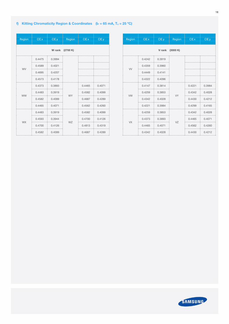
f) Kitting Chromaticity Region & Coordinates (IF = 65 mA, Ts = 25 ºC)
18
f) Kitting Chromaticity Region & Coordinates (IF = 65 mA, Ts = 25 ºC)
Region CIE x CIE y Region CIE x CIE y
W rank (2700 K)
WV
0.4475 0.3994
0.4589 0.4021
0.4695 0.4207
0.4573 0.4178
WW
0.4373 0.3893
WY
0.4465 0.4071
0.4483 0.3919 0.4582 0.4099
0.4582 0.4099 0.4687 0.4289
0.4465 0.4071 0.4562 0.4260
WX
0.4483 0.3919
WZ
0.4582 0.4099
0.4593 0.3944 0.4700 0.4126
0.4700 0.4126 0.4813 0.4319
0.4582 0.4099 0.4687 0.4289
Region CIE x CIE y Region CIE x CIE y
V rank (3000 K)
VV
0.4242 0.3919
0.4359 0.3960
0.4449 0.4141
0.4322 0.4096
VW
0.4147 0.3814
VY
0.4221 0.3984
0.4259 0.3853 0.4342 0.4028
0.4342 0.4028 0.4430 0.4212
0.4221 0.3984 0.4299 0.4165
VX
0.4259 0.3853
VZ
0.4342 0.4028
0.4373 0.3893 0.4465 0.4071
0.4465 0.4071 0.4562 0.4260
0.4342 0.4028 0.4430 0.4212

19
f) Kitting Chromaticity Region & Coordinates
Region CIE x CIE y Region CIE x CIE y
U rank (3500 K)
UV
0.3981 0.3800
0.4116 0.3865
0.4186 0.4037
0.4040 0.3966
UW
0.3889 0.3690
UY
0.3941 0.3848
0.4017 0.3751 0.4080 0.3916
0.4080 0.3916 0.4146 0.4089
0.3941 0.3848 0.3996 0.4015
UX
0.4017 0.3751
UZ
0.4080 0.3916
0.4147 0.3814 0.4221 0.3984
0.4221 0.3984 0.4299 0.4165
0.4080 0.3916 0.4146 0.4089
Region CIE x CIE y Region CIE x CIE y
T rank (4000 K)
TV
0.3744 0.3685
0.3863 0.3758
0.3912 0.3917
0.3782 0.3837
TW
0.3670 0.3578
TY
0.3702 0.3722
0.3783 0.3646 0.3825 0.3798
0.3825 0.3798 0.3869 0.3958
0.3702 0.3722 0.3736 0.3874
TX
0.3783 0.3646
TZ
0.3825 0.3798
0.3898 0.3716 0.3950 0.3875
0.3950 0.3875 0.4006 0.4044
0.3825 0.3798 0.3869 0.3958

20
f) Kitting Chromaticity Region & Coordinates
Region CIE x CIE y Region CIE x CIE y
R rank (5000 K)
RV
0.3407 0.3460
0.3485 0.3524
0.3500 0.3655
0.3415 0.3588
RW
0.3366 0.3369
RY
0.3371 0.3493
0.3440 0.3427 0.3411 0.3525
0.3446 0.3491 0.3415 0.3588
0.3407 0.3460 0.3457 0.3621
RX
0.3440 0.3428
RZ
0.3457 0.3621
0.3514 0.3487 0.3500 0.3655
0.3533 0.3620 0.3492 0.3587
0.3492 0.3587 0.3533 0.3620
Region CIE x CIE y Region CIE x CIE y
Q rank (5700 K)
QV
0.3256 0.3331
0.3331 0.3398
0.3333 0.3518
0.3252 0.3444
QW
0.3222 0.3243
QY
0.3215 0.3353
0.3294 0.3306 0.3293 0.3423
0.3293 0.3423 0.3292 0.3539
0.3215 0.3353 0.3207 0.3462
QX
0.3294 0.3306
QZ
0.3293 0.3423
0.3366 0.3369 0.3371 0.3493
0.3371 0.3493 0.3376 0.3616
0.3293 0.3423 0.3292 0.3539

21
f) Kitting Chromaticity Region & Coordinates
Region CIE x CIE y Region CIE x CIE y
P rank (6500 K)
PV
0.3098 0.3199
0.3177 0.3278
0.3166 0.3384
0.3080 0.3298
PW
0.3068 0.3113
PY
0.3048 0.3207
0.3144 0.3186 0.3130 0.3290
0.3130 0.3290 0.3115 0.3391
0.3089 0.3249 0.3028 0.3304
PX
0.3144 0.3186
PZ
0.3130 0.3290
0.3221 0.3261 0.3213 0.3373
0.3213 0.3373 0.3205 0.3481
0.3130 0.3290 0.3115 0.3391
Note:
Samsung maintains measurement tolerance of: Cx, Cy = ±0.005

22
3. Typical Characteristics Graphs
a) Spectrum Distribution (IF = 65 mA, Ts = 25 ºC)
CCT: 2700 K (80 CRI) CCT: 3000 K (80 CRI)
CCT: 3500 K (80 CRI) CCT: 4000 K (80 CRI)
CCT: 5000 K (80 CRI) CCT: 5700 K (80 CRI)

23
CCT: 6500 K (80 CRI)
b) Forward Current Characteristics (Ts = 25 ºC)
c) Temperature Characteristics (IF = 65 mA)

24
d) Color Shift Characteristics Ts = 25 ºC IF = 65 mA
e) Derating Curve
f) Beam Angle Characteristics (IF = 65 mA, Ts = 25 ºC)

25
4. Outline Drawing & Dimension
Notes:
1) This LED has built-in ESD protection device(s) connected in parallel to LED chip(s).
2) Ts point and measurement method:
① Measure one point at the cathode pad, if necessary remove PSR of PCB to reach Ts point.
② All pads must be soldered to the PCB to dissipate heat properly, otherwise the LED can be damaged.
Precautions:
1) Pressure on the LEDs will influence to the reliability of the LEDs. Precautions should be taken to avoid strong pressure on
the LEDs. Do not put stress on the LEDs during heating.
2) Re-soldering should not be done after the LEDs have been soldered. If re-soldering is unavoidable, LED`s characteristics
should be carefully checked before and after such repair.
3) Do not stack assembled PCBs together. Since materials of LEDs is soft, abrasion between two PCB assembled with LED
might cause catastrophic failure of the LEDs.
• Measurement unit: mm • Tolerance is ±0.10mm • Maximum compressing force is 15 N on the body ⓐ • Do not place pressure on the encapsulation resin ⓑ
ⓐ ⓑ
Tape Ts point
26
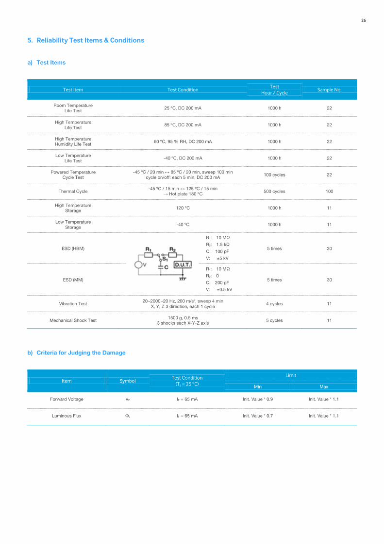
5. Reliability Test Items & Conditions
a) Test Items
Test Item Test Condition Test
Hour / Cycle Sample No.
Room Temperature Life Test 25 ºC, DC 200 mA 1000 h 22
High Temperature Life Test
85 ºC, DC 200 mA 1000 h 22
High Temperature Humidity Life Test 60 ºC, 95 % RH, DC 200 mA 1000 h 22
Low Temperature Life Test -40 ºC, DC 200 mA 1000 h 22
Powered Temperature Cycle Test
-45 ºC / 20 min ↔ 85 ºC / 20 min, sweep 100 min cycle on/off: each 5 min, DC 200 mA 100 cycles 22
Thermal Cycle -45 ºC / 15 min ↔ 125 ºC / 15 min
→ Hot plate 180 ºC 500 cycles 100
High Temperature Storage 120 ºC 1000 h 11
Low Temperature Storage
-40 ºC 1000 h 11
ESD (HBM)
R1: 10 MΩ
R2: 1.5 kΩ
C: 100 pF
V: ±5 kV
5 times 30
ESD (MM)
R1: 10 MΩ
R2: 0
C: 200 pF
V: ±0.5 kV
5 times 30
Vibration Test 20~2000~20 Hz, 200 m/s2, sweep 4 min X, Y, Z 3 direction, each 1 cycle
4 cycles 11
Mechanical Shock Test 1500 g, 0.5 ms 3 shocks each X-Y-Z axis 5 cycles 11
b) Criteria for Judging the Damage
Item Symbol Test Condition
(Ts = 25 ºC)
Limit
Min Max
Forward Voltage VF IF = 65 mA Init. Value * 0.9 Init. Value * 1.1
Luminous Flux Φv IF = 65 mA Init. Value * 0.7 Init. Value * 1.1

27
6. Soldering Conditions
a) Reflow Conditions (Pb free)
Reflow frequency: 2 times max.
b) Manual Soldering Conditions
Not more than 5 seconds @ max. 300 ºC, under soldering iron.
28
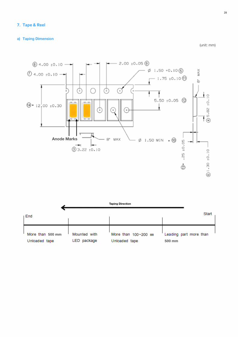
7. Tape & Reel
a) Taping Dimension
(unit: mm)
Taping Direction
500 mm
500 mm
Anode Marks
29
b-1) Reel Dimension(Max 2,500 pcs)
(unit: mm)
b-2) Reel Dimension (Max 10,000 pcs)
Symbol A B C W1 W2
Spec(mm) Ø330±1 80±1 13±0.5 13±0.3 17.5±1
Notes:
1) Quantity: The quantity/reel is 2,500 pcs
2) Cumulative Tolerance: Cumulative tolerance / 10 pitches is ±0.2 mm
3) Adhesion Strength of Cover Tape: Adhesion strength is 0.1-0.7 N when the cover tape is turned off from the carrier tape
at 10° angle to the carrier tape
4) Packaging: P/N, Manufacturing data code no. and quantity are indicated on the aluminum packing bag

30
A1R1S5 SPMWHT541ML5XAR0S0 A1R1S5 01 IIIIIIIIIIIIIIIIIIIIIIIIIIIIIIIIIIIIIIIIIIIIIIIII GLAYC4001 / 1001 / 2,500 pcs IIIIIIIIIIIIIIIIIIIIIIIIIIIIIIIIIIIIIIIIII
Bin Code
Product Code
Lot Number
A1R1S5 SPMWHT541ML5XAR0S0 A1R1S5 01 IIIIIIIIIIIIIIIIIIIIIIIIIIIIIIIIIIIIIIIIIIIIIIIII ①②③④⑤⑥⑦⑧⑨/1ⓐⓑⓒ/ 2,500 pcs IIIIIIIIIIIIIIIIIIIIIIIIIIIIIIIIIIIIIIIIII
8. Label Structure
a) Label Structure
Note: Denoted bin code and product code above is only an example (see description on page 5)
Bin Code:
ⓐⓑ: Forward Voltage bin (refer to page 8)
ⓒⓓ: Chromaticity bin (refer to page 10-13)
ⓔⓕ: Luminous Flux bin (refer to page 8)
b) Lot Number
The lot number is composed of the following characters:
①②③④⑤⑥⑦⑧⑨ / 1ⓐⓑⓒ / 2,500 pcs
① : Production site (S: Giheung, Korea, G: Tianjin, China)
② : L (LED)
③ : Product state (A: Normal, B: Bulk, C: First Production, R: Reproduction, S: Sample)
④ : Year (Z: 2015, A: 2016, B: 2017…)
⑤ : Month (1~9, A, B, C)
⑥⑦⑧⑨ : Day (1~9, A, B~V)
ⓐⓑⓒ : Product serial number (001 ~ 999)
ⓐⓑⓒⓓⓔⓕ

31
A1R1S5 SPMWHT541ML5XAR0S0 A1R1S5 01 IIIIIIIIIIIIIIIIIIIIIIIIIIIIIIIIIIIIIIIIIIIIIIIII GLAYC4001 / 1001 / 2,500 pcs IIIIIIIIIIIIIIIIIIIIIIIIIIIIIIIIIIIIIIIIII
A1R1S5 SPMWHT541ML5XAR0S0 A1R1S5 01 IIIIIIIIIIIIIIIIIIIIIIIIIIIIIIIIIIIIIIIIIIIIIIIII GLAYC4001 / 1001 / 25,000 pcs IIIIIIIIIIIIIIIIIIIIIIIIIIIIIIIIIIIIIIIIII
A1R1S5 SPMWHT541ML5XAR0S0 A1R1S5 01 IIIIIIIIIIIIIIIIIIIIIIIIIIIIIIIIIIIIIIIIIIIIIIIII GLAYC4001 / 1001 / 2,500 pcs IIIIIIIIIIIIIIIIIIIIIIIIIIIIIIIIIIIIIIIIII
9. Packing Structure
a-1) Packing Process (The quantity of PKG on the Reel to be Max 2,500pcs)
Material: Paper (SW3B(B))
Type Size (mm)
Note L W H
7 inch L 245 ± 5 220 ± 5 182 ± 5 Up to 10 reels
7 inch S 245 ± 5 220 ± 5 86 ± 5 Up to 5 reels
Reel
Aluminum Vinyl Packing Bag
Outer Box
LED
① H
W
L
① Side Label

32
A1R1S4 SPMWHT541ML5XKR0S0 A1R1S5 01 IIIIIIIIIIIIIIIIIIIIIIIIIIIIIIIIIIIIIIIIIIIIIIIII GLAZC4001 / 1001 / 10,000 pcs IIIIIIIIIIIIIIIIIIIIIIIIIIIIIIIIIIIIIIIIII
A1R1S4 SPMWHT541MP5WKR0S4 A1R1S4 01 IIIIIIIIIIIIIIIIIIIIIIIIIIIIIIIIIIIIIIIIIIIIIIIII GLAZC4001 / 1001 / 25,000 pcs IIIIIIIIIIIIIIIIIIIIIIIIIIIIIIIIIIIIIIIIII
A1R1S4 SPMWHT541ML5XKR0S0 A1R1S5 01 IIIIIIIIIIIIIIIIIIIIIIIIIIIIIIIIIIIIIIIIIIIIIIIII GLAZC4001 / 1001 / 10,000 pcs IIIIIIIIIIIIIIIIIIIIIIIIIIIIIIIIIIIIIIIIII
a-2) Packing Process (The quantity of PKG on the Reel to be Max 10,000pcs)
Aluminum Vinyl Packing Bag
② Side Label
Reel
A1R1S4 SPMWHT541ML5XKR0S0 A1R1S5 01 IIIIIIIIIIIIIIIIIIIIIIIIIIIIIIIIIIIIIIIIIIIIIIIII GLAZC4001 / 1001 / 150,000 pcs IIIIIIIIIIIIIIIIIIIIIIIIIIIIIIIIIIIIIIIIII
[Box Label]

33
AY◇WS4 SPMWHT541ML5XA◇KS0 AY◇WS4 01
IIIIIIIIIIIIIIIIIIIIIIIIIIIIIIIIIIIIIIIIIIIIIIIII GLAW94001 / 1001 / 2,500 pcs
IIIIIIIIIIIIIIIIIIIIIIIIIIIIIIIIIIIIIIIIII
AY◇WS4 SPMWHT541ML5XA◇KS0 AY◇WS4 01
IIIIIIIIIIIIIIIIIIIIIIIIIIIIIIIIIIIIIIIIIIIIIIIII GLAW94001 / 1001 / 2,500 pcs
IIIIIIIIIIIIIIIIIIIIIIIIIIIIIIIIIIIIIIIIII
AY◇ZS4 SPMWHT541ML5XA◇KS0 AY◇ZS4 01
IIIIIIIIIIIIIIIIIIIIIIIIIIIIIIIIIIIIIIIIIIIIIIIII GLAW94001 / 1001 / 2,500 pcs
IIIIIIIIIIIIIIIIIIIIIIIIIIIIIIIIIIIIIIIIII
AY◇ZS4 SPMWHT541ML5XA◇KS0 AY◇ZS4 01
IIIIIIIIIIIIIIIIIIIIIIIIIIIIIIIIIIIIIIIIIIIIIIIII GLAW94001 / 1001 / 2,500 pcs
IIIIIIIIIIIIIIIIIIIIIIIIIIIIIIIIIIIIIIIIII
AY◇WS4 SPMWHT541ML5XA◇KS0 AY◇WS4 01
IIIIIIIIIIIIIIIIIIIIIIIIIIIIIIIIIIIIIIIIIIIIIIIII GLAW94001 / 1001 / 25,000 pcs
IIIIIIIIIIIIIIIIIIIIIIIIIIIIIIIIIIIIIIIIII [BOX Label]
AY◇ZS4 SPMWHT541ML5XA◇KS0 AY◇ZS4 01
IIIIIIIIIIIIIIIIIIIIIIIIIIIIIIIIIIIIIIIIIIIIIIIII GLAW94001 / 1001 / 25,000 pcs
IIIIIIIIIIIIIIIIIIIIIIIIIIIIIIIIIIIIIIIIII [BOX Label]
b-1) Packing Process for kitting (The quantity of PKG on the Reel to be Max 2,500pcs)
Material: Paper (SW3B(B))
Type Size (mm)
Note L W H
7 inch L 245 ± 5 220 ± 5 182 ± 5 Up to 10 reels
Reel
Kitting ‘A’
Kitting ‘A’ Kitting ‘B’
Aluminum Vinyl Packing Bag
Kitting ‘A’ Kitting ‘B’
Kitting ‘B’
Outer Box
Kitting ‘A’ Kitting ‘B’
LED
Note: "◇" can be Nominal CCT code.

34
A1◇WS4 SPMWHT541ML5XK◇KS0 AY◇WS4 01
IIIIIIIIIIIIIIIIIIIIIIIIIIIIIIIIIIIIIIIIIIIIIIIII GLAW94001 / 1001 / 10,000 pcs
IIIIIIIIIIIIIIIIIIIIIIIIIIIIIIIIIIIIIIIIII
A1◇ZS4 SPMWHT541ML5XK◇KS0 AY◇WS4 01
IIIIIIIIIIIIIIIIIIIIIIIIIIIIIIIIIIIIIIIIIIIIIIIII GLAW94001 / 1001 / 10,000 pcs
IIIIIIIIIIIIIIIIIIIIIIIIIIIIIIIIIIIIIIIIII
A1◇WS4 SPMWHT541ML5XK◇KS0 AY◇WS4 01
IIIIIIIIIIIIIIIIIIIIIIIIIIIIIIIIIIIIIIIIIIIIIIIII GLAW94001 / 1001 / 10,000 pcs
IIIIIIIIIIIIIIIIIIIIIIIIIIIIIIIIIIIIIIIIII [BOX Label]
A1◇ZS4 SPMWHT541ML5XK◇KS0 AY◇WS4 01
IIIIIIIIIIIIIIIIIIIIIIIIIIIIIIIIIIIIIIIIIIIIIIIII GLAW94001 / 1001 / 10,000 pcs
IIIIIIIIIIIIIIIIIIIIIIIIIIIIIIIIIIIIIIIIII [BOX Label]
b-2) Packing Process for kitting (The quantity of PKG on the Reel to be Max 10,000pcs)
Material: Paper (SW3B(B))
Type Size (mm)
Note L W H
13 inch L 345 ± 5 378 ± 5 405 ± 5 Up to 10 reels
LED
Aluminum Vinyl Packing Bag
Reel
Kitting ‘A’
Kitting ‘A’ Kitting ‘B’
Kitting ‘B’
Kitting ‘A’ Kitting ‘B’
Outer Box
Kitting ‘A’ Kitting ‘B’
Note: "◇" can be Nominal CCT code.
AB AB AB AB AB
35
b) Aluminum Vinyl Packing Bag
c) Silica Gel & Humidity Indicator Card inside Aluminum Vinyl Bag
A1R1S5 SPMWHT541ML5XAR0S0 A1R1S5 01 IIIIIIIIIIIIIIIIIIIIIIIIIIIIIIIIIIIIIIIIIIIIIIIII GLAYC4001 / 1001 / 2,500 pcs IIIIIIIIIIIIIIIIIIIIIIIIIIIIIIIIIIIIIIIIII

36
10. Precautions in Handling & Use
1) For over-current protection, users are recommended to apply resistors connected in series with the LEDs to mitigate
sudden change of the forward current caused by shift of forward voltage.
2) This device should not be used in any type of fluid such as water, oil, organic solvent, etc. When cleaning is required,
IPA is recommended as the cleaning agent. Some solvent-based cleaning agent may damage the silicone resins used
in the device.
3) When the device is in operation, the forward current should be carefully determined considering the maximum ambient
temperature and corresponding junction temperature.
4) LEDs must be stored in a clean environment. If the LEDs are to be stored for three months or more after being shipped
from Samsung, they should be packed with a nitrogen-filled container (shelf life of sealed bags is 12 months at
temperature 0~40 ºC, 0~90 % RH).
5) After storage bag is opened, device subjected to soldering, solder reflow, or other high temperature processes must be:
a. Mounted within 672 hours (28 days) at an assembly line with a condition of no more than 30 ºC / 60 % RH, or
b. Stored at <10 % RH
6) Repack unused devices with anti-moisture packing, fold to close any opening and then store in a dry place.
7) Devices require baking before mounting, if humidity card reading is >60 % at 23 ± 5 ºC.
8) Devices must be baked for 10~24 hours at 60 ± 5 ºC, if baking is required.
9) The LEDs are sensitive to the static electricity and surge current. It is recommended to use a wrist band or anti-
electrostatic glove when handling the LEDs. If voltage exceeding the absolute maximum rating is applied to LEDs, it
may cause damage or even destruction to LED devices. Damaged LEDs may show some unusual characteristics such
as increase in leakage current, lowered turn-on voltage, or abnormal lighting of LEDs at low current.
10) VOCs (Volatile Organic Compounds) can be generated from adhesives, flux, hardener or organic additives used in
luminaires (fixtures). Transparent LED silicone encapsulant is permeable to those chemicals and they may lead to a
discoloration of encapsulant when they exposed to heat or light. This phenomenon can cause a significant loss of light
emitted (output) from the luminaires. In order to prevent these problems, we recommend users to know the physical
properties of materials used in luminaires and they must be carefully selected.
11) Risk of sulfurization (or tarnishing)
The LED from Samsung uses a silver-plated lead frame and its surface color may change to black (or dark colored) when
it is exposed to sulfur (S), chlorine (Cl) or other halogen compound. Sulfurization of lead frame may cause intensity
degradation, change of chromaticity coordinates and, in extreme cases, open circuit. It requires caution. Due to possible
sulfurization of lead frame, LED should not be used and stored together with oxidizing substances made of materials
such as rubber, plain paper, lead solder cream, etc.

Legal and additional information.
About Samsung Electronics Co., Ltd.
Samsung Electronics Co., Ltd. inspires the world and shapes the future with
transformative ideas and technologies that redefine the worlds of TVs, smartphones,
wearable devices, tablets, cameras, digital appliances, printers, medical equipment,
network systems, and semiconductor and LED solutions. We are also leading in the
Internet of Things space with the open platform SmartThings, our broad range of smart
devices, and through proactive cross-industry collaboration. We employ 319,000 people
across 84 countries with annual sales of US $196 billion. To discover more, and for the
latest news, feature articles and press material, please visit the Samsung Newsroom at
news.samsung.com.
Copyright © 2015 Samsung Electronics Co., Ltd. All rights reserved.
Samsung is a registered trademark of Samsung Electronics Co., Ltd.
Specifications and designs are subject to change without notice. Non-metric
weights and measurements are approximate. All data were deemed correct
at time of creation. Samsung is not liable for errors or omissions. All brand, product,
service names and logos are trademarks and/or registered trademarks of their
respective owners and are hereby recognized and acknowledged.
Samsung Electronics Co., Ltd.
95, Samsung 2-ro
Giheung-gu
Yongin-si, Gyeonggi-do, 446-711
KOREA
www.samsungled.com