Embed Size (px)
Citation preview

VOUT
SSRESRT
COMP
FB
RAMP
PGND
CSG
CS
LO
SW
HO
HB
VCCVIN
AGND
UVLO
VCCDIS
DEMB
CM
VIN
VOUT
SW
LM5117
Product
Folder
Sample &Buy
Technical
Documents
Tools &
Software
Support &Community
LM5117, LM5117-Q1SNVS698F –APRIL 2011–REVISED AUGUST 2015
LM5117/Q1 Wide Input Range Synchronous Buck Controller with Analog Current Monitor1 Features 3 Description
The LM5117 is a synchronous buck controller1• LM5117-Q1 is Qualified for Automotive
intended for step-down regulator applications from aApplicationshigh voltage or widely varying input supply. The
• AEC-Q100 Qualified With the Following Results: control method is based upon current mode control– Device Temperature Grade 1: -40°C to 125°C utilizing an emulated current ramp. Current mode
control provides inherent line feed-forward, cycle-by-Ambient Operating Temperature Rangecycle current limiting and ease of loop compensation.• Emulated Peak Current Mode ControlThe use of an emulated control ramp reduces noise
• Wide Operating Range from 5.5 V to 65 V sensitivity of the pulse-width modulation circuit,• Robust 3.3-A Peak Gate Drives allowing reliable control of very small duty cycles
necessary in high input voltage applications.• Adaptive Dead-Time Output Driver Control• Free-Run or Synchronizable Clock up to 750 kHz The operating frequency is programmable from 50
kHz to 750 kHz. The LM5117 drives external high-• Optional Diode Emulation Modeside and low-side NMOS power switches with• Programmable Output from 0.8 V adaptive dead-time control. A user-selectable diode
• Precision 1.5% Voltage Reference emulation mode enables discontinuous modeoperation for improved efficiency at light load• Analog Current Monitorconditions. A high voltage bias regulator that allows• Programmable Current Limit external bias supply further improves efficiency. The
• Hiccup Mode Overcurrent Protection LM5117’s unique analog telemetry feature providesaverage output current information. Additional• Programmable Soft-Start and Trackingfeatures include thermal shutdown, frequency• Programmable Line Undervoltage Lockoutsynchronization, hiccup mode current limit, and• Programmable Switchover to External Bias Supply adjustable line undervoltage lockout.
• Thermal ShutdownDevice Information(1)
2 Applications PART NUMBER PACKAGE BODY SIZE (NOM)LM5117 HTSSOP (20) PWP 6.50 mm × 4.40 mm• Automotive InfotainmentLM5117-Q1 WQFN (24) RTW 4.00 mm × 4.00 mm• Industrial DC-DC Motor Drivers(1) For all available packages, see the orderable addendum at• Automotive USB Power
the end of the datasheet.• Telecom Server
Typical Application
1
An IMPORTANT NOTICE at the end of this data sheet addresses availability, warranty, changes, use in safety-critical applications,intellectual property matters and other important disclaimers. PRODUCTION DATA.
LM5117, LM5117-Q1SNVS698F –APRIL 2011–REVISED AUGUST 2015 www.ti.com
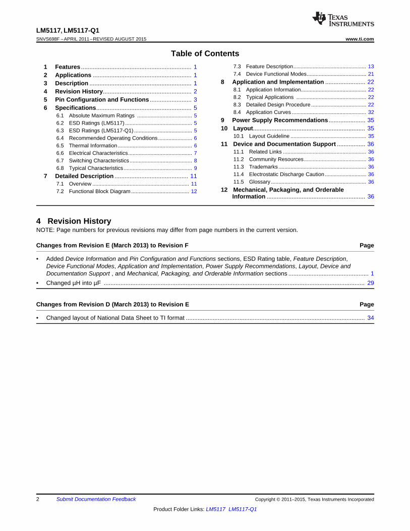
Table of Contents7.3 Feature Description................................................. 131 Features .................................................................. 17.4 Device Functional Modes........................................ 212 Applications ........................................................... 1
8 Application and Implementation ........................ 223 Description ............................................................. 18.1 Application Information............................................ 224 Revision History..................................................... 28.2 Typical Applications ............................................... 225 Pin Configuration and Functions ......................... 38.3 Detailed Design Procedure ..................................... 226 Specifications......................................................... 58.4 Application Curves .................................................. 326.1 Absolute Maximum Ratings ..................................... 5
9 Power Supply Recommendations ...................... 356.2 ESD Ratings (LM5117) ............................................. 510 Layout................................................................... 356.3 ESD Ratings (LM5117-Q1) ....................................... 5
10.1 Layout Guideline ................................................... 356.4 Recommended Operating Conditions....................... 611 Device and Documentation Support ................. 366.5 Thermal Information .................................................. 6
11.1 Related Links ........................................................ 366.6 Electrical Characteristics........................................... 711.2 Community Resources.......................................... 366.7 Switching Characteristics .......................................... 811.3 Trademarks ........................................................... 366.8 Typical Characteristics .............................................. 911.4 Electrostatic Discharge Caution............................ 367 Detailed Description ............................................ 1111.5 Glossary ................................................................ 367.1 Overview ................................................................. 11
12 Mechanical, Packaging, and Orderable7.2 Functional Block Diagram ....................................... 12Information ........................................................... 36
4 Revision HistoryNOTE: Page numbers for previous revisions may differ from page numbers in the current version.
Changes from Revision E (March 2013) to Revision F Page
• Added Device Information and Pin Configuration and Functions sections, ESD Rating table, Feature Description,Device Functional Modes, Application and Implementation, Power Supply Recommendations, Layout, Device andDocumentation Support , and Mechanical, Packaging, and Orderable Information sections ................................................ 1
• Changed µH into µF ............................................................................................................................................................ 29
Changes from Revision D (March 2013) to Revision E Page
• Changed layout of National Data Sheet to TI format ........................................................................................................... 34
2 Submit Documentation Feedback Copyright © 2011–2015, Texas Instruments Incorporated
Product Folder Links: LM5117 LM5117-Q1

PGND
UV
LO
AGND
DEMB
RES
SS
RT
FB
CO
MP
CM
1
6
2
3
4
5
8 9
20
14
15
19
18
17
16
13
1211
VIN
LO
HB
HO
SW
VCC
CSG
CS
RA
MP
21222324
VC
CD
IS
7 10
NC
NC
NC
NC
EP
UVLO
AGND
DEMB
RES
SS
RT
FB
COMP
CM
VIN
PGND
LO
HB
HO
SW
VCC
CSG
CS
RAMP
1
6
2
3
4
5
8
9
20
14
15
19
18
17
16
13
12
11
EP
VCCDIS
10
7
LM5117, LM5117-Q1www.ti.com SNVS698F –APRIL 2011–REVISED AUGUST 2015
5 Pin Configuration and Functions
PWP Package20-Pin HTSSOP
Top View
RTW Package24-Pin WQFN
Top View
Copyright © 2011–2015, Texas Instruments Incorporated Submit Documentation Feedback 3
Product Folder Links: LM5117 LM5117-Q1
LM5117, LM5117-Q1SNVS698F –APRIL 2011–REVISED AUGUST 2015 www.ti.com
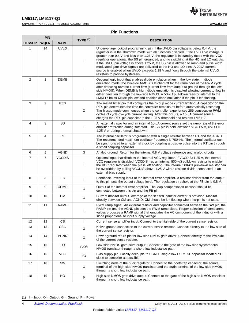
Pin FunctionsPIN
TYPE (1) DESCRIPTIONHTSSOP WQFN NAME
1 24 UVLO Undervoltage lockout programming pin. If the UVLO pin voltage is below 0.4 V, theregulator is in the shutdown mode with all functions disabled. If the UVLO pin voltage isgreater than 0.4 V and less than 1.25 V, the regulator is in standby mode with the VCCregulator operational, the SS pin grounded, and no switching at the HO and LO outputs.I If the UVLO pin voltage is above 1.25 V, the SS pin is allowed to ramp and pulse widthmodulated gate drive signals are delivered to the HO and LO pins. A 20μA currentsource is enabled when UVLO exceeds 1.25 V and flows through the external UVLOresistors to provide hysteresis.
2 1 DEMB Optional logic input that enables diode emulation when in the low state. In diodeemulation mode, the low-side NMOS is latched off for the remainder of the PWM cycleafter detecting reverse current flow (current flow from output to ground through the low-I side NMOS). When DEMB is high, diode emulation is disabled allowing current to flow ineither direction through the low-side NMOS. A 50-kΩ pull-down resistor internal to theLM5117 holds DEMB pin low and enables diode emulation if the pin is left floating.
3 2 RES The restart timer pin that configures the hiccup mode current limiting. A capacitor on theRES pin determines the time the controller remains off before automatically restarting.
O The hiccup mode commences when the controller experiences 256 consecutive PWMcycles of cycle-by-cycle current limiting. After this occurs, a 10-μA current sourcecharges the RES pin capacitor to the 1.25 V threshold and restarts LM5117.
4 3 SS An external capacitor and an internal 10-μA current source set the ramp rate of the errorI amplifier reference during soft-start. The SS pin is held low when VCC< 5 V, UVLO <
1.25 V or during thermal shutdown.5 4 RT The internal oscillator is programmed with a single resistor between RT and the AGND.
The recommended maximum oscillator frequency is 750kHz. The internal oscillator canI be synchronized to an external clock by coupling a positive pulse into the RT pin througha small coupling capacitor.
6 5 AGND G Analog ground. Return for the internal 0.8 V voltage reference and analog circuits.7 7 VCCDIS Optional input that disables the internal VCC regulator. If VCCDIS>1.25 V, the internal
VCC regulator is disabled. VCCDIS has an internal 500-kΩ pulldown resistor to enableI the VCC regulator when the pin is left floating. The internal 500-kΩ pull-down resistor can
be overridden by pulling VCCDIS above 1.25 V with a resistor divider connected to anexternal bias supply.
8 8 FB Feedback. Inverting input of the internal error amplifier. A resistor divider from the outputI to this pin sets the output voltage level. The regulation threshold at the FB pin is 0.8 V.9 9 COMP Output of the internal error amplifier. The loop compensation network should beO connected between this pin and the FB pin.10 10 CM Current monitor output. Average of the sensed inductor current is provided. MonitorO directly between CM and AGND. CM should be left floating when the pin is not used.11 11 RAMP PWM ramp signal. An external resistor and capacitor connected between the SW pin, the
RAMP pin and the AGND pin sets the PWM ramp slope. Proper selection of componentI values produces a RAMP signal that emulates the AC component of the inductor with aslope proportional to input supply voltage.
12 12 CS I Current sense amplifier input. Connect to the high-side of the current sense resistor.13 13 CSG Kelvin ground connection to the current sense resistor. Connect directly to the low-side ofG the current sense resistor.14 14 PGND Power ground return pin for low-side NMOS gate driver. Connect directly to the low-sideO of the current sense resistor.15 15 LO Low-side NMOS gate drive output. Connect to the gate of the low-side synchronousP/O/I NMOS transistor through a short, low inductance path.16 16 VCC Bias supply pin. Locally decouple to PGND using a low ESR/ESL capacitor located asI/O close to controller as possible.17 18 SW Switching node of the buck regulator. Connect to the bootstrap capacitor, the source
O terminal of the high-side NMOS transistor and the drain terminal of the low-side NMOSthrough a short, low inductance path.
18 19 HO High-side NMOS gate drive output. Connect to the gate of the high-side NMOS transistorP through a short, low inductance path.
(1) I = Input, O = Output, G = Ground, P = Power
4 Submit Documentation Feedback Copyright © 2011–2015, Texas Instruments Incorporated
Product Folder Links: LM5117 LM5117-Q1

LM5117, LM5117-Q1www.ti.com SNVS698F –APRIL 2011–REVISED AUGUST 2015
Pin Functions (continued)PIN
TYPE (1) DESCRIPTIONHTSSOP WQFN NAME
19 20 HB High-side driver supply for the bootstrap gate drive. Connect to the cathode of theexternal bootstrap diode and to the bootstrap capacitor. The bootstrap capacitor suppliesP/I current to charge the high-side NMOS gate and should be placed as close to controlleras possible.
20 22 VIN P/I Supply voltage input source for the VCC regulator.EP EP EP Exposed pad of the package. Electrically isolated. Should be soldered to the ground- plane to reduce thermal resistance.
6 NC - No electrical contact.17 NC - No electrical contact.21 NC - No electrical contact.23 NC - No electrical contact.
6 Specifications
6.1 Absolute Maximum Ratingsover operating free-air temperature range (unless otherwise noted) (1)
MIN MAX UNITVIN to AGND –0.3 75 VSW to AGND –3.0 75 VHB to SW –0.3 15 VVCC to AGND (2) –0.3 15 VHO to SW –0.3 HB + 0.3 VLO to AGND –0.3 VCC + 0.3 VFB, DEMB, RES, VCCDIS, UVLO to AGND –0.3 15 VCM, COMP to AGND (3) –0.3 7 VSS, RAMP, RT to AGND –0.3 7 VCS, CSG, PGND, to AGND –0.3 0.3 VStorage Temperature, Tstg –55 150 °CJunction temperature –40 150 °C
(1) Stresses beyond those listed under Absolute Maximum Ratings may cause permanent damage to the device. These are stress ratingsonly, which do not imply functional operation of the device at these or any other conditions beyond those indicated under RecommendedOperating Conditions. Exposure to absolute-maximum-rated conditions for extended periods may affect device reliability.
(2) See Application and Implementation when input supply voltage is less than the VCC voltage.(3) These pins are output pins. As such they are not specified to have an external voltage applied.
6.2 ESD Ratings (LM5117)VALUE UNIT
Human-body model (HBM), per ANSI/ESDA/JEDEC JS-001 (1) ±2000 VV(ESD) Electrostatic discharge Charged-device model (CDM), per JEDEC specification JESD22- V ±750 VC101 (2)
(1) JEDEC document JEP155 states that 500-V HBM allows safe manufacturing with a standard ESD control process.(2) JEDEC document JEP157 states that 250-V CDM allows safe manufacturing with a standard ESD control process.
6.3 ESD Ratings (LM5117-Q1)VALUE UNIT
Human-body model (HBM), per AEC Q100-002 (1) ±2000 VV(ESD) Electrostatic discharge
Charged-device model (CDM), per AEC Q100-011 ±750 V
(1) AEC Q100-002 indicates that HBM stressing shall be in accordance with the ANSI/ESDA/JEDEC JS-001 specification.
Copyright © 2011–2015, Texas Instruments Incorporated Submit Documentation Feedback 5
Product Folder Links: LM5117 LM5117-Q1
LM5117, LM5117-Q1SNVS698F –APRIL 2011–REVISED AUGUST 2015 www.ti.com
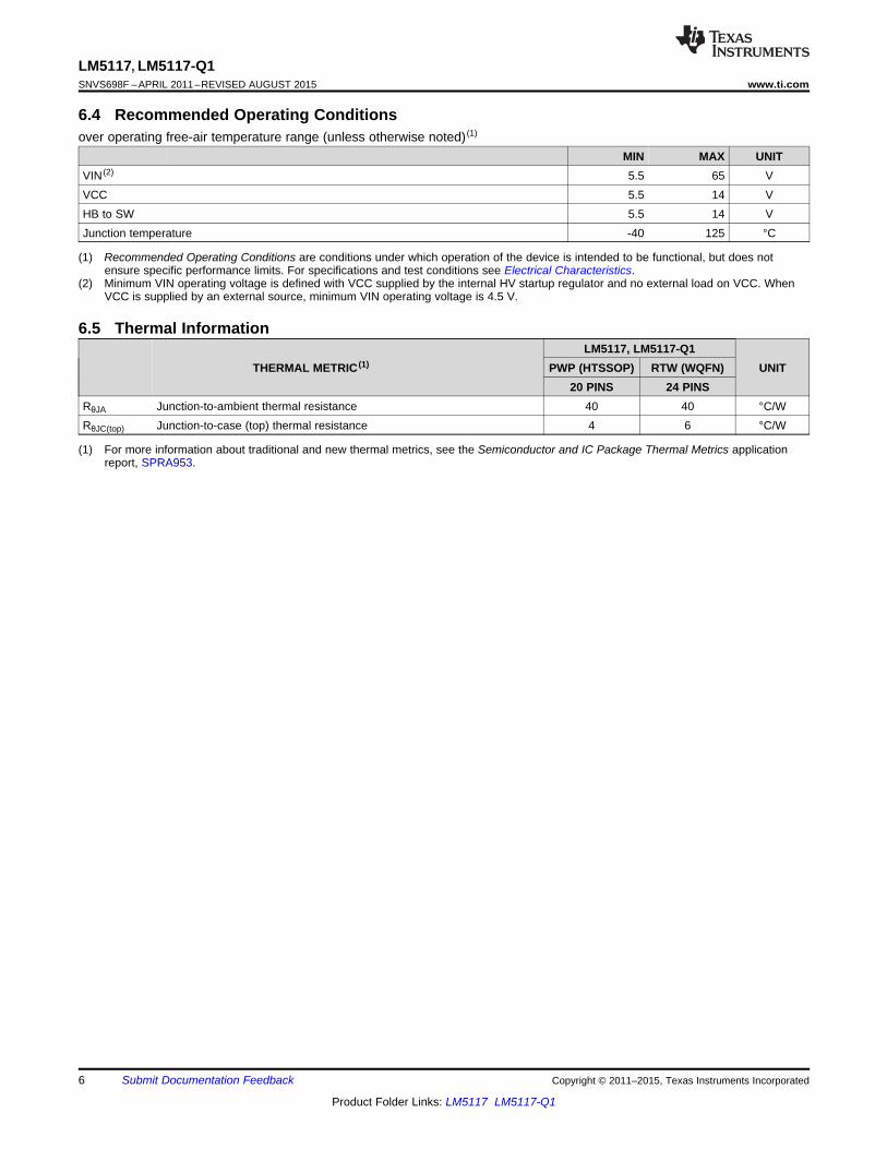
6.4 Recommended Operating Conditionsover operating free-air temperature range (unless otherwise noted) (1)
MIN MAX UNITVIN (2) 5.5 65 VVCC 5.5 14 VHB to SW 5.5 14 VJunction temperature -40 125 °C
(1) Recommended Operating Conditions are conditions under which operation of the device is intended to be functional, but does notensure specific performance limits. For specifications and test conditions see Electrical Characteristics.
(2) Minimum VIN operating voltage is defined with VCC supplied by the internal HV startup regulator and no external load on VCC. WhenVCC is supplied by an external source, minimum VIN operating voltage is 4.5 V.
6.5 Thermal InformationLM5117, LM5117-Q1
THERMAL METRIC (1) PWP (HTSSOP) RTW (WQFN) UNIT20 PINS 24 PINS
RθJA Junction-to-ambient thermal resistance 40 40 °C/WRθJC(top) Junction-to-case (top) thermal resistance 4 6 °C/W
(1) For more information about traditional and new thermal metrics, see the Semiconductor and IC Package Thermal Metrics applicationreport, SPRA953.
6 Submit Documentation Feedback Copyright © 2011–2015, Texas Instruments Incorporated
Product Folder Links: LM5117 LM5117-Q1

LM5117, LM5117-Q1www.ti.com SNVS698F –APRIL 2011–REVISED AUGUST 2015
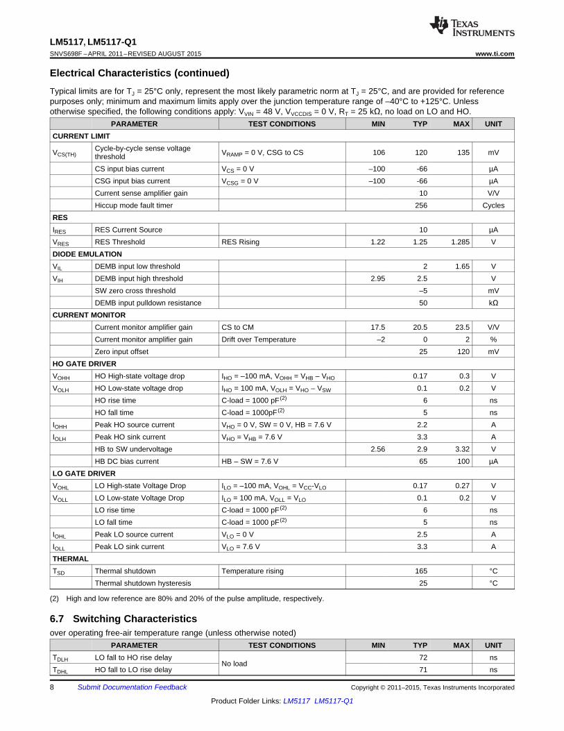
6.6 Electrical CharacteristicsTypical limits are for TJ = 25°C only, represent the most likely parametric norm at TJ = 25°C, and are provided for referencepurposes only; minimum and maximum limits apply over the junction temperature range of –40°C to +125°C. Unlessotherwise specified, the following conditions apply: VVIN = 48 V, VVCCDIS = 0 V, RT = 25 kΩ, no load on LO and HO.
PARAMETER TEST CONDITIONS MIN TYP MAX UNITVIN SUPPLY
VSS = 0 V 4.8 6.2 mAIBIAS VIN operating current (1)
VSS = 0 V, VVCCDIS = 2 V 0.4 0.55 mAISHUTDOWN VIN shutdown current VSS = 0 V, VUVLO = 0 V 16 40 µAVCC REGULATORVCC(REG) VCC regulation No load 6.85 7.6 8.2 V
VVIN = 5.5 V, No external load 0.05 0.14 VVCC dropout (VIN to VCC)
VVIN = 6 V, ICC = 20 mA 0.4 0.5 VVCC sourcing current limit VVCC = 0 V 30 42 mA
VSS = 0 V, VVCCDIS = 2 V 4 5 mAIVCC VCC operating current (1) VSS = 0 V, VVCCDIS = 2 V, VVCC = 14 5.8 7.3 mAV
VCC undervoltage threshold VCC rising 4.7 4.9 5.15 VVCC undervoltage hysteresis 0.2 V
VCC DISABLEVCCDIS threshold VCCDIS rising 1.22 1.25 1.29 VVCCDIS hysteresis 0.06 VVCCDIS input current VVCCDIS = 0 V -20 nAVCCDIS pulldown resistance 500 kΩ
UVLOUVLO threshold UVLO rising 1.22 1.25 1.29 VUVLO hysteresis current VUVLO = 1.4 V 15 20 25 µAUVLO shutdown threshold UVLO falling 0.23 0.3 VUVLO shutdown hysteresis 0.1 V
SOFT STARTISS SS current source VSS = 0 V 7 10 12 µA
SS pulldown resistance 13 24 ΩERROR AMPLIFIERVREF FB reference voltage Measured at FB, FB = COMP 788 800 812 mV
FB input bias current VFB = 0.8 V 1 nAVOH COMP output high voltage ISOURCE = 3 mA 2.8 VVOL COMP output low voltage ISINK = 3 mA 0.26 VAOL DC gain 80 dBƒBW Unity gain bandwidth 3 MHzPWM COMPARATORtHO(OFF) Forced HO Off-time 260 320 440 nstON(MIN) Minimum HO On-time VVIN = 65 V 100 ns
COMP to PWM comparator offset 1.2 VOSCILLATORƒSW1 Frequency 1 RT = 25 kΩ 180 200 220 kHzƒSW2 Frequency 2 RT = 10 kΩ 430 480 530 kHz
RT output voltage 1.25 VRT sync positive threshold 2.6 3.2 3.95 VSync pulse width 100 ns
(1) Operating current does not include the current into the RT resistor.
Copyright © 2011–2015, Texas Instruments Incorporated Submit Documentation Feedback 7
Product Folder Links: LM5117 LM5117-Q1
LM5117, LM5117-Q1SNVS698F –APRIL 2011–REVISED AUGUST 2015 www.ti.com
Electrical Characteristics (continued)Typical limits are for TJ = 25°C only, represent the most likely parametric norm at TJ = 25°C, and are provided for referencepurposes only; minimum and maximum limits apply over the junction temperature range of –40°C to +125°C. Unlessotherwise specified, the following conditions apply: VVIN = 48 V, VVCCDIS = 0 V, RT = 25 kΩ, no load on LO and HO.
PARAMETER TEST CONDITIONS MIN TYP MAX UNITCURRENT LIMIT
Cycle-by-cycle sense voltageVCS(TH) VRAMP = 0 V, CSG to CS 106 120 135 mVthresholdCS input bias current VCS = 0 V –100 -66 µACSG input bias current VCSG = 0 V –100 -66 µACurrent sense amplifier gain 10 V/VHiccup mode fault timer 256 Cycles
RESIRES RES Current Source 10 µAVRES RES Threshold RES Rising 1.22 1.25 1.285 VDIODE EMULATIONVIL DEMB input low threshold 2 1.65 VVIH DEMB input high threshold 2.95 2.5 V
SW zero cross threshold –5 mVDEMB input pulldown resistance 50 kΩ
CURRENT MONITORCurrent monitor amplifier gain CS to CM 17.5 20.5 23.5 V/VCurrent monitor amplifier gain Drift over Temperature –2 0 2 %Zero input offset 25 120 mV
HO GATE DRIVERVOHH HO High-state voltage drop IHO = –100 mA, VOHH = VHB – VHO 0.17 0.3 VVOLH HO Low-state voltage drop IHO = 100 mA, VOLH = VHO – VSW 0.1 0.2 V
HO rise time C-load = 1000 pF (2) 6 nsHO fall time C-load = 1000pF (2) 5 ns
IOHH Peak HO source current VHO = 0 V, SW = 0 V, HB = 7.6 V 2.2 AIOLH Peak HO sink current VHO = VHB = 7.6 V 3.3 A
HB to SW undervoltage 2.56 2.9 3.32 VHB DC bias current HB – SW = 7.6 V 65 100 µA
LO GATE DRIVERVOHL LO High-state Voltage Drop ILO = –100 mA, VOHL = VCC-VLO 0.17 0.27 VVOLL LO Low-state Voltage Drop ILO = 100 mA, VOLL = VLO 0.1 0.2 V
LO rise time C-load = 1000 pF (2) 6 nsLO fall time C-load = 1000 pF (2) 5 ns
IOHL Peak LO source current VLO = 0 V 2.5 AIOLL Peak LO sink current VLO = 7.6 V 3.3 ATHERMALTSD Thermal shutdown Temperature rising 165 °C
Thermal shutdown hysteresis 25 °C
(2) High and low reference are 80% and 20% of the pulse amplitude, respectively.
6.7 Switching Characteristicsover operating free-air temperature range (unless otherwise noted)
PARAMETER TEST CONDITIONS MIN TYP MAX UNITTDLH LO fall to HO rise delay 72 ns
No loadTDHL HO fall to LO rise delay 71 ns
8 Submit Documentation Feedback Copyright © 2011–2015, Texas Instruments Incorporated
Product Folder Links: LM5117 LM5117-Q1
LM5117, LM5117-Q1www.ti.com SNVS698F –APRIL 2011–REVISED AUGUST 2015
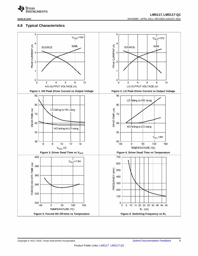
6.8 Typical Characteristics
Figure 1. HO Peak Driver Current vs Output Voltage Figure 2. LO Peak Driver Current vs Output Voltage
Figure 3. Driver Dead Time vs VVCC Figure 4. Driver Dead Time vs Temperature
Figure 5. Forced HO Off-time vs Temperature Figure 6. Switching Frequency vs RT
Copyright © 2011–2015, Texas Instruments Incorporated Submit Documentation Feedback 9
Product Folder Links: LM5117 LM5117-Q1

LM5117, LM5117-Q1SNVS698F –APRIL 2011–REVISED AUGUST 2015 www.ti.com
Typical Characteristics (continued)
Figure 7. VVCC vs IVCC Figure 8. VVCC vs VVIN
Figure 9. VCS(TH) vs Temperature Figure 10. VREF vs Temperature
Figure 12. Error Amp Gain and Phase vs FrequencyFigure 11. VVCC vs Temperature
10 Submit Documentation Feedback Copyright © 2011–2015, Texas Instruments Incorporated
Product Folder Links: LM5117 LM5117-Q1

LM5117, LM5117-Q1www.ti.com SNVS698F –APRIL 2011–REVISED AUGUST 2015
Typical Characteristics (continued)
Figure 13. VCM vs IOUT Figure 14. VCM vs VCSG-CS
7 Detailed Description
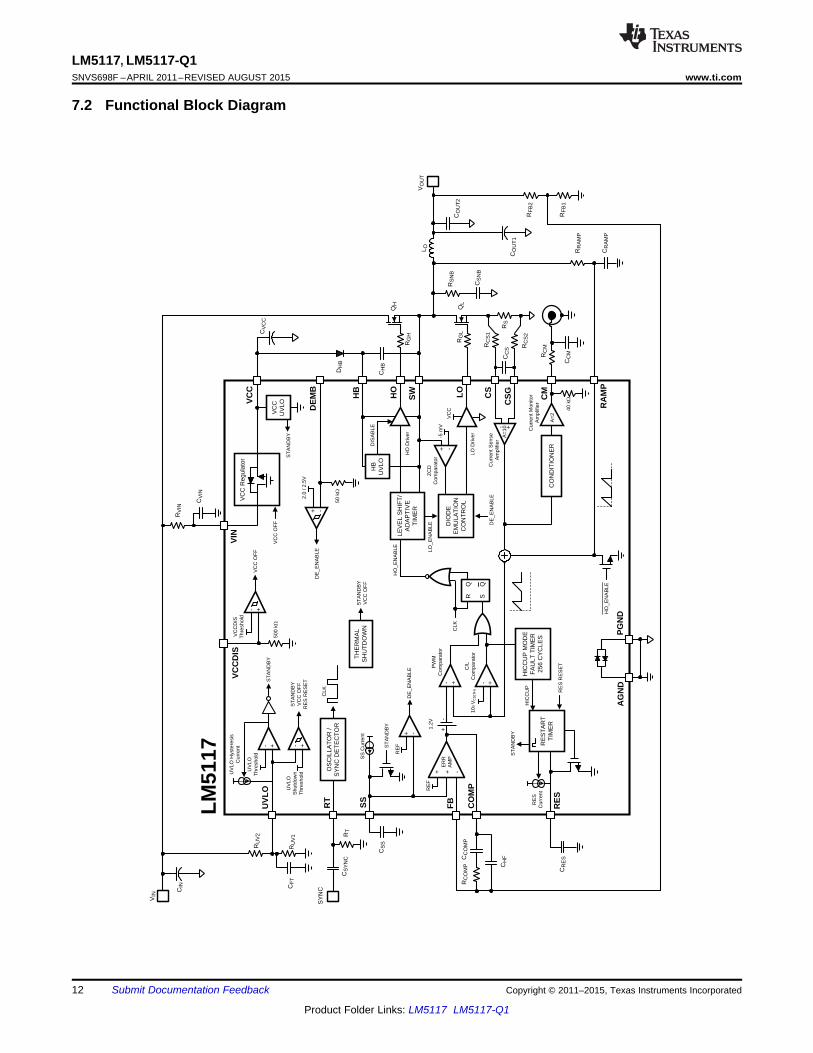
7.1 OverviewThe LM5117 high voltage switching controller features all of the functions necessary to implement an efficienthigh voltage buck regulator that operates over a very wide input voltage range. This easy to use controllerintegrates high-side and low-side NMOS drivers. The regulator control method is based upon peak current modecontrol utilizing an emulated current ramp. Peak current mode control provides inherent line feed-forward, cycle-by-cycle current limiting and ease of loop compensation. The use of an emulated control ramp reduces noisesensitivity of the PWM circuit, allowing reliable processing of the very small duty cycles necessary in high inputvoltage applications.
The switching frequency is user programmable up to 750 kHz. The RT pin allows the switching frequency to beprogrammed by a single resistor or synchronized to an external clock. Fault protection features include cycle-by-cycle and hiccup mode current limiting, thermal shutdown and remote shutdown capability by pulling down UVLOpin. The UVLO input enables the regulator when the input voltage reaches a user selected threshold andprovides a very low quiescent shutdown current when pulled low. A unique analog telemetry feature providesaveraged output current information, allowing various applications that need either a current monitor or currentcontrol. The functional block diagram and typical application circuit of the LM5117 are shown in Functional BlockDiagram.
The device is available in a HTSSOP-20 (6.5 mm x 4.4 mm) package, as well as a WQFN-24 (4 mm × 4 mm)package which features an exposed pad to aid in thermal dissipation.
Copyright © 2011–2015, Texas Instruments Incorporated Submit Documentation Feedback 11
Product Folder Links: LM5117 LM5117-Q1
RT
RE
S
AG
ND
RE
F
DIS
AB
LE
VC
C
HO
Driv
er
LO D
river
LEV
EL
SH
IFT
/A
DA
PT
IVE
T
IME
R
+-
SRQ Q
CLK
+- +-
-+
+ + -
1.2V
DE
MB
SS
Cur
rent
VIN
VC
CU
VLO
VC
C O
FF
FBSS
HB
HO
SW LO
CS
PG
ND
CO
MP
CS
G
CM
VC
C R
egul
ator
TH
ER
MA
L S
HU
TD
OW
N
UV
LO
Shu
tdow
n T
hres
hold
ST
AN
DB
YS
TA
ND
BY
VC
C O
FF
RE
S R
ES
ET
UV
LO
Thr
esho
ld
UV
LO H
yste
resi
s C
urre
nt R
ES
TA
RT
T
IME
R
HIC
CU
P M
OD
E
FA
ULT
TIM
ER
256
CY
CLE
SR
ES
C
urre
nt
UV
LO
VC
C
ST
AN
DB
Y
DE
_EN
AB
LE+ -
ST
AN
DB
Y
RE
S R
ES
ET
HIC
CU
P
10uV
CS
(TH
)
PW
M
Com
para
tor
C/L
C
ompa
rato
r
50 k:
+-
+ -D
E_E
NA
BLE
2.0
/ 2.5
V
OS
CIL
LAT
OR
/S
YN
C D
ET
EC
TO
R
CLK
A=
2
40 k:
CO
ND
ITIO
NE
R
Cur
rent
Sen
se
Am
plifi
er
RA
MP
HO
_EN
AB
LE
+-
+ -
ZC
DC
ompa
rato
r-5
mV
DIO
DE
E
MU
LAT
ION
C
ON
TR
OL
LO_E
NA
BLE
ER
R
AM
P
VC
CD
IS
500
k:
VC
CD
IS
Thr
esho
ld
VC
C O
FF
+-
DE
_EN
AB
LE
LM
5117 R
EF
VO
UT
VIN
CIN
CO
UT
1
CO
UT
2
L O
QH
QL
RS
NB
CS
NB
RS
RG
H
RG
L
DH
B
CV
CC
CC
S RC
S2
RC
S1
CH
B
RV
IN
CV
IN
SY
NCC
FT
CR
AM
P
RR
AM
P
RF
B2
RF
B1
RC
OM
PC
CO
MP
CH
F
CS
YN
CR
T
CR
ES
CS
SRU
V2
RU
V1
RC
M
CC
M
ST
AN
DB
Y
ST
AN
DB
YV
CC
OF
F
HO
_EN
AB
LE
HB
UV
LO
Cur
rent
Mon
itor
Am
plifi
er
A=
10
LM5117, LM5117-Q1SNVS698F –APRIL 2011–REVISED AUGUST 2015 www.ti.com
7.2 Functional Block Diagram
12 Submit Documentation Feedback Copyright © 2011–2015, Texas Instruments Incorporated
Product Folder Links: LM5117 LM5117-Q1
VCC
VCCDIS
LM5117
VOUT
VCCDIS resistor divider is required when external VCC supplying voltage is smaller than 8.5V
SW
VCC
VCCDIS
LM5117
VOUT
VCCDIS resistor divider is required when external VCC supplying voltage is smaller than 8.5V
VIN
LM5117
VIN
VCCExternal
VCC Supply
LM5117, LM5117-Q1www.ti.com SNVS698F –APRIL 2011–REVISED AUGUST 2015
7.3 Feature Description
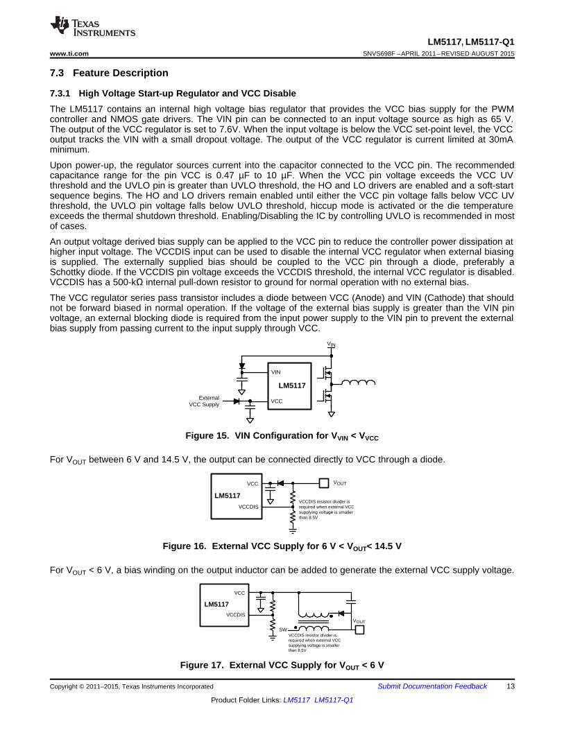
7.3.1 High Voltage Start-up Regulator and VCC DisableThe LM5117 contains an internal high voltage bias regulator that provides the VCC bias supply for the PWMcontroller and NMOS gate drivers. The VIN pin can be connected to an input voltage source as high as 65 V.The output of the VCC regulator is set to 7.6V. When the input voltage is below the VCC set-point level, the VCCoutput tracks the VIN with a small dropout voltage. The output of the VCC regulator is current limited at 30mAminimum.
Upon power-up, the regulator sources current into the capacitor connected to the VCC pin. The recommendedcapacitance range for the pin VCC is 0.47 µF to 10 µF. When the VCC pin voltage exceeds the VCC UVthreshold and the UVLO pin is greater than UVLO threshold, the HO and LO drivers are enabled and a soft-startsequence begins. The HO and LO drivers remain enabled until either the VCC pin voltage falls below VCC UVthreshold, the UVLO pin voltage falls below UVLO threshold, hiccup mode is activated or the die temperatureexceeds the thermal shutdown threshold. Enabling/Disabling the IC by controlling UVLO is recommended in mostof cases.
An output voltage derived bias supply can be applied to the VCC pin to reduce the controller power dissipation athigher input voltage. The VCCDIS input can be used to disable the internal VCC regulator when external biasingis supplied. The externally supplied bias should be coupled to the VCC pin through a diode, preferably aSchottky diode. If the VCCDIS pin voltage exceeds the VCCDIS threshold, the internal VCC regulator is disabled.VCCDIS has a 500-kΩ internal pull-down resistor to ground for normal operation with no external bias.
The VCC regulator series pass transistor includes a diode between VCC (Anode) and VIN (Cathode) that shouldnot be forward biased in normal operation. If the voltage of the external bias supply is greater than the VIN pinvoltage, an external blocking diode is required from the input power supply to the VIN pin to prevent the externalbias supply from passing current to the input supply through VCC.
Figure 15. VIN Configuration for VVIN < VVCC
For VOUT between 6 V and 14.5 V, the output can be connected directly to VCC through a diode.
Figure 16. External VCC Supply for 6 V < VOUT< 14.5 V
For VOUT < 6 V, a bias winding on the output inductor can be added to generate the external VCC supply voltage.
Figure 17. External VCC Supply for VOUT < 6 V
Copyright © 2011–2015, Texas Instruments Incorporated Submit Documentation Feedback 13
Product Folder Links: LM5117 LM5117-Q1

LM5117VIN
UVLO Shutdown Threshold SHUTDOWN
UVLO Threshold
UVLO Hysteresis Current
UVLO
+-
+-
CFT
RUV2
RUV1
STANDBY
VCC
LM5117
VOUT
Zener
R1
R1 is required to limit maximum reverse zener current 30 k: minimum resistive loss at VCC guarantees minimum reverse zener current
30 k:
LM5117, LM5117-Q1SNVS698F –APRIL 2011–REVISED AUGUST 2015 www.ti.com
Feature Description (continued)For 14.5 V <VOUT, the external supply voltage can be regulated by using a series Zener diode from the output toVCC.
Figure 18. External VCC Supply for 14.5 V < VOUT
In high input voltage applications, extra care should be taken to ensure the VIN pin does not exceed the absolutemaximum voltage rating of 75V. During line or load transients, voltage ringing on the VIN that exceeds theAbsolute Maximum Rating can damage the IC. Both careful PC board layout and the use of quality bypasscapacitors located close to the VIN and AGND pin are essential. Adding an R-C filter (RVIN, CVIN) on VIN isoptional and helps to prevent faulty operation caused by poor PC board layout and high frequency switchingnoise injection. The recommended capacitance and resistance range are 0.1 µF to 10 µF and 1 Ω to 10 Ω.
7.3.2 UVLOThe LM5117 contains a dual level UVLO (under-voltage lockout) circuit. When the UVLO is less than 0.4 V, theLM5117 is in shutdown mode. The shutdown comparator provides 100 mV of hysteresis to avoid chatter duringtransitions. When the UVLO pin voltage is greater than 0.4 V but less than 1.25 V, the controller is in standbymode. In the standby mode, the VCC bias regulator is active but the HO and LO drivers are disabled and the SSpin is held low. This feature allows the UVLO pin to be used as a remote shutdown function by pulling the UVLOpin down below 0.4 V with an external open collector or open drain device. When the VCC pin exceeds its under-voltage lockout threshold and the UVLO pin voltage is greater than 1.25 V, the HO and LO drivers are enabledand normal operation begins.
Figure 19. UVLO Configuration
The UVLO pin should not be left floating. An external UVLO set-point voltage divider from the VIN to AGND isused to set the minimum input operating voltage of the regulator. The divider must be designed such that thevoltage at the UVLO pin is greater than 1.25 V and never exceeds 15 V when the input voltage is in the desiredoperating range. If necessary, the UVLO pin can be clamped with a Zener diode.
UVLO hysteresis is accomplished with an internal 20μA current source that is switched on or off into theimpedance of the UVLO set-point divider. When the UVLO pin voltage exceeds the 1.25 V threshold, the currentsource is enabled to quickly raise the voltage at the UVLO pin. When the UVLO pin voltage falls below the 1.25V threshold, the current source is disabled causing the voltage at the UVLO pin to quickly fall. The use of a CFTcapacitor in parallel with RUV1 helps to minimize switching noise injection into UVLO pin, but it may slow downthe falling speed of the UVLO pin when the 20 μA current source is disabled. The recommended range for CFT is10 pF to 220 pF.
14 Submit Documentation Feedback Copyright © 2011–2015, Texas Instruments Incorporated
Product Folder Links: LM5117 LM5117-Q1
5.2 x 10⁹
RT = - 948 [5]fSW
1.25V x RUV2RUV1 = VIN(STARTUP) - 1.25V
[5]
VHYSRUV2 = 20 µA
[5]
LM5117, LM5117-Q1www.ti.com SNVS698F –APRIL 2011–REVISED AUGUST 2015
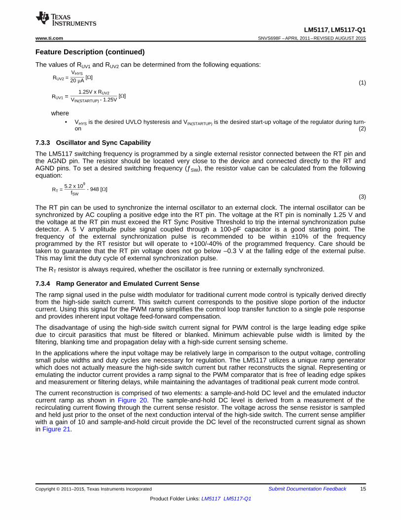
Feature Description (continued)The values of RUV1 and RUV2 can be determined from the following equations:
(1)
where• VHYS is the desired UVLO hysteresis and VIN(STARTUP) is the desired start-up voltage of the regulator during turn-
on (2)
7.3.3 Oscillator and Sync CapabilityThe LM5117 switching frequency is programmed by a single external resistor connected between the RT pin andthe AGND pin. The resistor should be located very close to the device and connected directly to the RT andAGND pins. To set a desired switching frequency (ƒSW), the resistor value can be calculated from the followingequation:
(3)
The RT pin can be used to synchronize the internal oscillator to an external clock. The internal oscillator can besynchronized by AC coupling a positive edge into the RT pin. The voltage at the RT pin is nominally 1.25 V andthe voltage at the RT pin must exceed the RT Sync Positive Threshold to trip the internal synchronization pulsedetector. A 5 V amplitude pulse signal coupled through a 100-pF capacitor is a good starting point. Thefrequency of the external synchronization pulse is recommended to be within ±10% of the frequencyprogrammed by the RT resistor but will operate to +100/-40% of the programmed frequency. Care should betaken to guarantee that the RT pin voltage does not go below –0.3 V at the falling edge of the external pulse.This may limit the duty cycle of external synchronization pulse.
The RT resistor is always required, whether the oscillator is free running or externally synchronized.
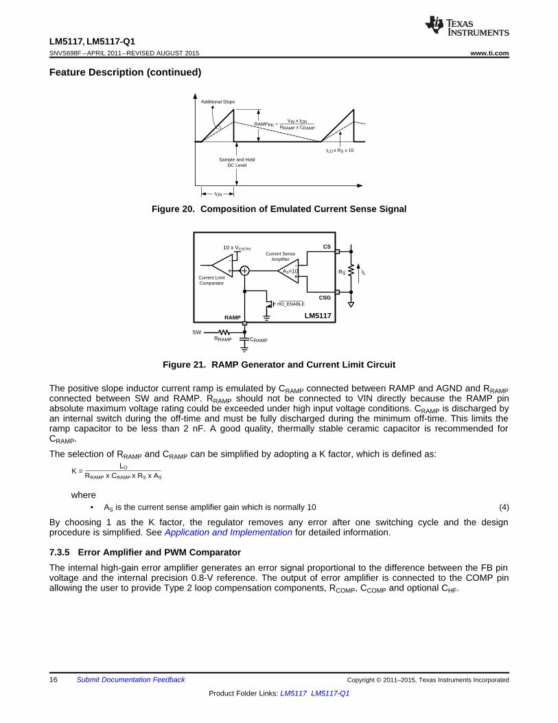
7.3.4 Ramp Generator and Emulated Current SenseThe ramp signal used in the pulse width modulator for traditional current mode control is typically derived directlyfrom the high-side switch current. This switch current corresponds to the positive slope portion of the inductorcurrent. Using this signal for the PWM ramp simplifies the control loop transfer function to a single pole responseand provides inherent input voltage feed-forward compensation.
The disadvantage of using the high-side switch current signal for PWM control is the large leading edge spikedue to circuit parasitics that must be filtered or blanked. Minimum achievable pulse width is limited by thefiltering, blanking time and propagation delay with a high-side current sensing scheme.
In the applications where the input voltage may be relatively large in comparison to the output voltage, controllingsmall pulse widths and duty cycles are necessary for regulation. The LM5117 utilizes a unique ramp generatorwhich does not actually measure the high-side switch current but rather reconstructs the signal. Representing oremulating the inductor current provides a ramp signal to the PWM comparator that is free of leading edge spikesand measurement or filtering delays, while maintaining the advantages of traditional peak current mode control.
The current reconstruction is comprised of two elements: a sample-and-hold DC level and the emulated inductorcurrent ramp as shown in Figure 20. The sample-and-hold DC level is derived from a measurement of therecirculating current flowing through the current sense resistor. The voltage across the sense resistor is sampledand held just prior to the onset of the next conduction interval of the high-side switch. The current sense amplifierwith a gain of 10 and sample-and-hold circuit provide the DC level of the reconstructed current signal as shownin Figure 21.
Copyright © 2011–2015, Texas Instruments Incorporated Submit Documentation Feedback 15
Product Folder Links: LM5117 LM5117-Q1
LO
RRAMP x CRAMP x RS x ASK =
HO_ENABLE
SW
CS
RAMP
CSG
+-
+-
AS=10
RRAMP CRAMP
RS IL
10 xVCS(TH)
Current Limit Comparator
Current Sense Amplifier
LM5117
Sample and Hold DC Level
tON
ILO x RS x 10
Additional Slope
VIN x tONRRAMP x CRAMP
RAMPPK =
LM5117, LM5117-Q1SNVS698F –APRIL 2011–REVISED AUGUST 2015 www.ti.com
Feature Description (continued)
Figure 20. Composition of Emulated Current Sense Signal
Figure 21. RAMP Generator and Current Limit Circuit
The positive slope inductor current ramp is emulated by CRAMP connected between RAMP and AGND and RRAMPconnected between SW and RAMP. RRAMP should not be connected to VIN directly because the RAMP pinabsolute maximum voltage rating could be exceeded under high input voltage conditions. CRAMP is discharged byan internal switch during the off-time and must be fully discharged during the minimum off-time. This limits theramp capacitor to be less than 2 nF. A good quality, thermally stable ceramic capacitor is recommended forCRAMP.
The selection of RRAMP and CRAMP can be simplified by adopting a K factor, which is defined as:
where• AS is the current sense amplifier gain which is normally 10 (4)
By choosing 1 as the K factor, the regulator removes any error after one switching cycle and the designprocedure is simplified. See Application and Implementation for detailed information.
7.3.5 Error Amplifier and PWM ComparatorThe internal high-gain error amplifier generates an error signal proportional to the difference between the FB pinvoltage and the internal precision 0.8-V reference. The output of error amplifier is connected to the COMP pinallowing the user to provide Type 2 loop compensation components, RCOMP, CCOMP and optional CHF.
16 Submit Documentation Feedback Copyright © 2011–2015, Texas Instruments Incorporated
Product Folder Links: LM5117 LM5117-Q1
10 µA
CSS x 0.8VtSS = [sec]
FP2 =1CCOMP x CHF
CCOMP + CHF2S x RCOMP x ¹
ᩤ
[Hz]
2Sx RCOMP x CCOMP
1FZ = [Hz]
FP1 = 0 [Hz]
VOUT
COMP
FB
LM5117
+-
RFB2
RFB1
RCOMP CCOMP
CHF
REF
Error Amplifier
Type 2 Compensation Components
- +
PWM Comparator
+-
RAMP Generator Output
(optional)
LM5117, LM5117-Q1www.ti.com SNVS698F –APRIL 2011–REVISED AUGUST 2015
Feature Description (continued)
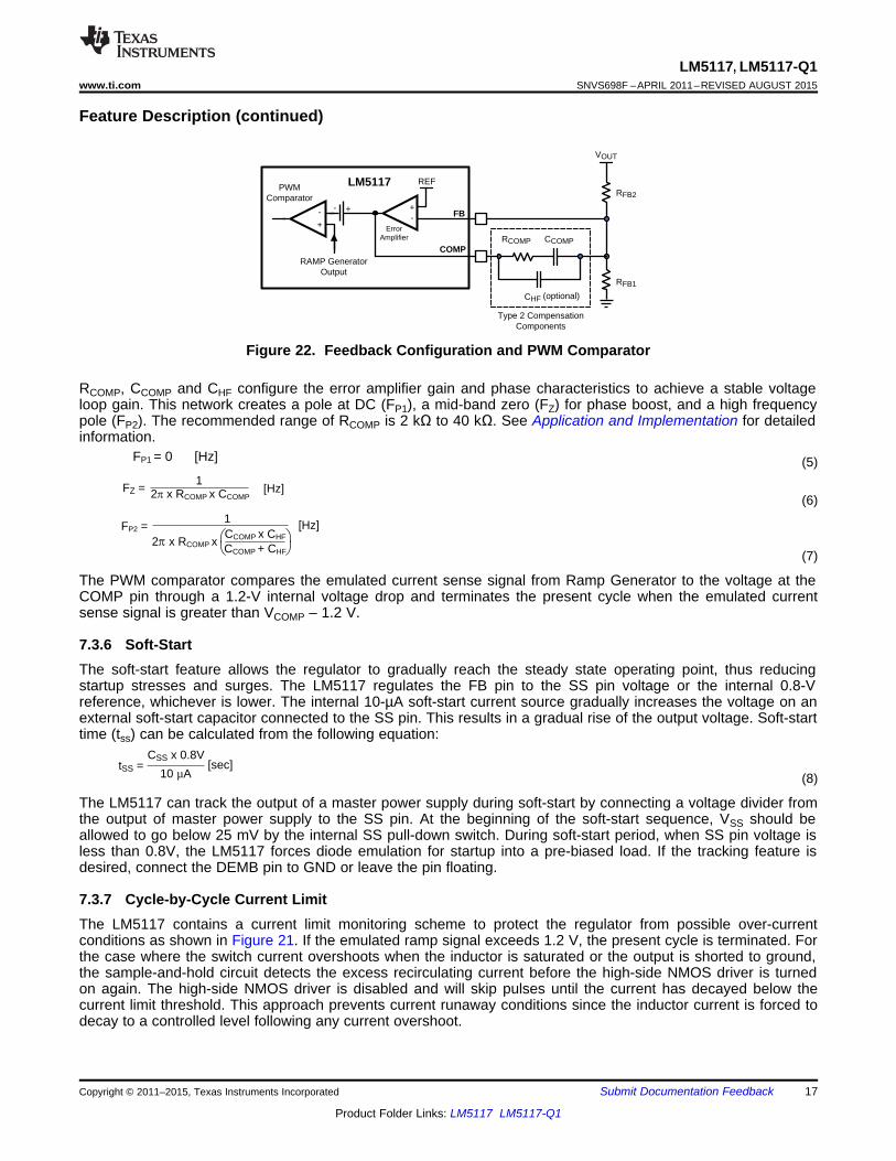
Figure 22. Feedback Configuration and PWM Comparator
RCOMP, CCOMP and CHF configure the error amplifier gain and phase characteristics to achieve a stable voltageloop gain. This network creates a pole at DC (FP1), a mid-band zero (FZ) for phase boost, and a high frequencypole (FP2). The recommended range of RCOMP is 2 kΩ to 40 kΩ. See Application and Implementation for detailedinformation.
(5)
(6)
(7)
The PWM comparator compares the emulated current sense signal from Ramp Generator to the voltage at theCOMP pin through a 1.2-V internal voltage drop and terminates the present cycle when the emulated currentsense signal is greater than VCOMP – 1.2 V.
7.3.6 Soft-StartThe soft-start feature allows the regulator to gradually reach the steady state operating point, thus reducingstartup stresses and surges. The LM5117 regulates the FB pin to the SS pin voltage or the internal 0.8-Vreference, whichever is lower. The internal 10-µA soft-start current source gradually increases the voltage on anexternal soft-start capacitor connected to the SS pin. This results in a gradual rise of the output voltage. Soft-starttime (tss) can be calculated from the following equation:
(8)
The LM5117 can track the output of a master power supply during soft-start by connecting a voltage divider fromthe output of master power supply to the SS pin. At the beginning of the soft-start sequence, VSS should beallowed to go below 25 mV by the internal SS pull-down switch. During soft-start period, when SS pin voltage isless than 0.8V, the LM5117 forces diode emulation for startup into a pre-biased load. If the tracking feature isdesired, connect the DEMB pin to GND or leave the pin floating.
7.3.7 Cycle-by-Cycle Current LimitThe LM5117 contains a current limit monitoring scheme to protect the regulator from possible over-currentconditions as shown in Figure 21. If the emulated ramp signal exceeds 1.2 V, the present cycle is terminated. Forthe case where the switch current overshoots when the inductor is saturated or the output is shorted to ground,the sample-and-hold circuit detects the excess recirculating current before the high-side NMOS driver is turnedon again. The high-side NMOS driver is disabled and will skip pulses until the current has decayed below thecurrent limit threshold. This approach prevents current runaway conditions since the inductor current is forced todecay to a controlled level following any current overshoot.
Copyright © 2011–2015, Texas Instruments Incorporated Submit Documentation Feedback 17
Product Folder Links: LM5117 LM5117-Q1

RS LO
VIN(MAX) x tON(MIN)+ILIM_PK =
VCS(TH)[A]
0
IOUT IPP
fSW
1T=
¸¹
ᬩ
§VIN
IPP = 1 -VOUT VOUT
xLO x fSW
[A]
2
IPPIL(MAX)_AVE = IL(MAX)_PK - [A]
VOUT
fSW x AS x RS x RRAMP x CRAMP+ IPP -
VCS(TH)
RSIL(MAX)_PK = [A]
LM5117, LM5117-Q1SNVS698F –APRIL 2011–REVISED AUGUST 2015 www.ti.com
Feature Description (continued)Maximum peak inductor current can be calculated as:
(9)
where• IPP represents inductor peak to peak ripple current in Figure 23, and is defined as: (10)
(11)
Figure 23. Inductor Current
During an output short condition, the worst case peak inductor current is limited to:
where• tON(MIN) is the minimum HO on-time (12)
In most cases, especially if the output voltage is relatively high, it is recommended that a soft-saturating inductorsuch as a powder core device is used. If a sharp-saturating inductor is used, the inductor saturation level mustbe above ILIM_PK. The temperatures of the NMOS devices, RS and inductor should be checked under this outputshort condition.
7.3.8 Hiccup Mode Current LimitingTo further protect the regulator during prolonged current limit conditions, LM5117 provides a hiccup mode currentlimit. An internal hiccup mode fault timer counts the PWM clock cycles during which cycle-by-cycle currentlimiting occurs. When the hiccup mode fault timer detects 256 consecutive cycles of current limiting, an internalrestart timer forces the controller to enter a low power dissipation standby mode and starts sourcing 10 μA ofcurrent into the RES pin capacitor CRES. In this standby mode, HO and LO outputs are disabled and the soft-startcapacitor CSS is discharged.
18 Submit Documentation Feedback Copyright © 2011–2015, Texas Instruments Incorporated
Product Folder Links: LM5117 LM5117-Q1
RES
LM5117
VCC
CRES
RES
LM5117
RES
LM5117
VCC
(a) Hiccup Mode Current Limit
(b) Latch-off Mode Current Limit
(c) Cycle-by-cycle Current Limit
RES
RESTART TIMER
HICCUP MODE FAULT TIMER256 CYCLES
RES Current
STANDBY
HICCUP
Current Limit Comparator
CRES
+-
LM5117
HO
LO
SS
RES0V
1.25V RES Threshold
0.8V REF
Current Limit Detected
Current Limit persists during 256 consecutive cycles
tSStRES
IRES = 10 µA
ISS = 10 µA
10 PA
CRES x 1.25VtRES = [sec]
LM5117, LM5117-Q1www.ti.com SNVS698F –APRIL 2011–REVISED AUGUST 2015
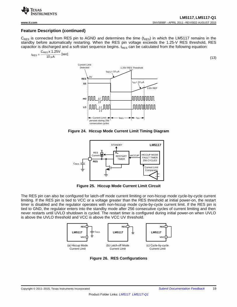
Feature Description (continued)CRES is connected from RES pin to AGND and determines the time (tRES) in which the LM5117 remains in thestandby before automatically restarting. When the RES pin voltage exceeds the 1.25-V RES threshold, REScapacitor is discharged and a soft-start sequence begins. tRES can be calculated from the following equation:
(13)
Figure 24. Hiccup Mode Current Limit Timing Diagram
Figure 25. Hiccup Mode Current Limit Circuit
The RES pin can also be configured for latch-off mode current limiting or non-hiccup mode cycle-by-cycle currentlimiting. If the RES pin is tied to VCC or a voltage greater than the RES threshold at initial power-on, the restarttimer is disabled and the regulator operates with non-hiccup mode cycle-by-cycle current limit. If the RES pin istied to GND, the regulator enters into the standby mode after 256 consecutive cycles of current limiting and thennever restarts until UVLO shutdown is cycled. The restart timer is configured during initial power-on when UVLOis above the UVLO threshold and VCC is above the VCC UV threshold.
Figure 26. RES Configurations
Copyright © 2011–2015, Texas Instruments Incorporated Submit Documentation Feedback 19
Product Folder Links: LM5117 LM5117-Q1
( ) [ ]CM_ AVE PEAK VALLEY S SV I I R A V= + ´ ´
CMAM = 2
40 k:
RCM
CCM
Current Monitor Amplifier
Current Sense Amplifier Output LM5117
CONDITIONER
LM5117, LM5117-Q1SNVS698F –APRIL 2011–REVISED AUGUST 2015 www.ti.com
Feature Description (continued)7.3.9 HO and LO DriversThe LM5117 contains high current NMOS drivers and an associated high-side level shifter to drive the externalhigh-side NMOS device. This high-side gate driver works in conjunction with an external diode DHB, andbootstrap capacitor CHB. A 0.1-μF or larger ceramic capacitor, connected with short traces between the HB andSW pin, is recommended. During the off-time of the high-side NMOS driver, the SW pin voltage is approximately0V and the CHB is charged from VCC through the DHB. When operating with a high PWM duty cycle, the high-side NMOS device is forced off each cycle for 320 ns to ensure that CHB is recharged.
The LO and HO outputs are controlled with an adaptive dead-time methodology which insures that both outputsare never enabled at the same time. When the controller commands HO to be enabled, the adaptive dead-timelogic first disables LO and waits for the LO voltage to drop. HO is then enabled after a small delay (LO Fall to HORise Delay). Similarly, the LO turn-on is delayed until the HO voltage has discharged. LO is then enabled after asmall delay (HO Fall to LO Rise Delay). This technique insures adequate dead-time for any size NMOS device,especially when VCC is supplied by a higher external voltage source. The adaptive dead-time circuitry monitorsthe voltages of HO and LO outputs and insures the dead-time between the HO and LO outputs. Adding a gateresister, RGH or RGL, may decrease the effective dead-time.
Care should be exercised in selecting an output NMOS device with the appropriate threshold voltage, especiallyif VCC is supplied by an external bias supply voltage below the VCC regulation level. During startup at low inputvoltages, the low-side NMOS device gate plateau voltage should be lower than the VCC under-voltage lockoutthreshold. Otherwise, there may be insufficient VCC voltage to completely enhance the NMOS device as theVCC under-voltage lockout is released during startup. If the high-side NMOS drive voltage is lower than the high-side NMOS device gate plateau voltage during startup, the regulator may not start or it may hang up momentarilyin a high power dissipation state. This condition can be addressed by selecting an NMOS device with a lowerthreshold voltage. This situation can be avoided if the minimum input voltage programmed by the UVLO resistoris above the VCC regulation level.
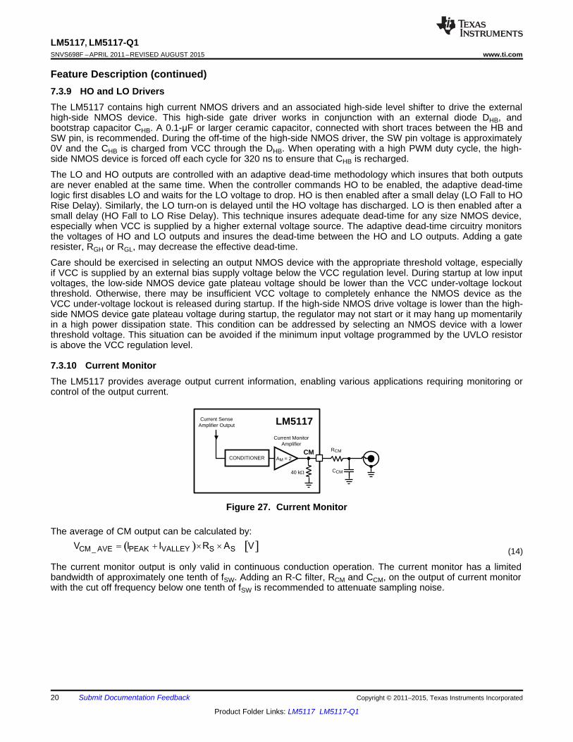
7.3.10 Current MonitorThe LM5117 provides average output current information, enabling various applications requiring monitoring orcontrol of the output current.
Figure 27. Current Monitor
The average of CM output can be calculated by:
(14)
The current monitor output is only valid in continuous conduction operation. The current monitor has a limitedbandwidth of approximately one tenth of fSW. Adding an R-C filter, RCM and CCM, on the output of current monitorwith the cut off frequency below one tenth of fSW is recommended to attenuate sampling noise.
20 Submit Documentation Feedback Copyright © 2011–2015, Texas Instruments Incorporated
Product Folder Links: LM5117 LM5117-Q1
LM5117, LM5117-Q1www.ti.com SNVS698F –APRIL 2011–REVISED AUGUST 2015
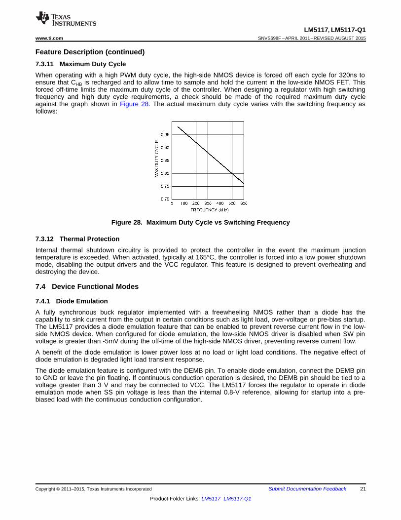
Feature Description (continued)7.3.11 Maximum Duty CycleWhen operating with a high PWM duty cycle, the high-side NMOS device is forced off each cycle for 320ns toensure that CHB is recharged and to allow time to sample and hold the current in the low-side NMOS FET. Thisforced off-time limits the maximum duty cycle of the controller. When designing a regulator with high switchingfrequency and high duty cycle requirements, a check should be made of the required maximum duty cycleagainst the graph shown in Figure 28. The actual maximum duty cycle varies with the switching frequency asfollows:
Figure 28. Maximum Duty Cycle vs Switching Frequency
7.3.12 Thermal ProtectionInternal thermal shutdown circuitry is provided to protect the controller in the event the maximum junctiontemperature is exceeded. When activated, typically at 165°C, the controller is forced into a low power shutdownmode, disabling the output drivers and the VCC regulator. This feature is designed to prevent overheating anddestroying the device.
7.4 Device Functional Modes
7.4.1 Diode EmulationA fully synchronous buck regulator implemented with a freewheeling NMOS rather than a diode has thecapability to sink current from the output in certain conditions such as light load, over-voltage or pre-bias startup.The LM5117 provides a diode emulation feature that can be enabled to prevent reverse current flow in the low-side NMOS device. When configured for diode emulation, the low-side NMOS driver is disabled when SW pinvoltage is greater than -5mV during the off-time of the high-side NMOS driver, preventing reverse current flow.
A benefit of the diode emulation is lower power loss at no load or light load conditions. The negative effect ofdiode emulation is degraded light load transient response.
The diode emulation feature is configured with the DEMB pin. To enable diode emulation, connect the DEMB pinto GND or leave the pin floating. If continuous conduction operation is desired, the DEMB pin should be tied to avoltage greater than 3 V and may be connected to VCC. The LM5117 forces the regulator to operate in diodeemulation mode when SS pin voltage is less than the internal 0.8-V reference, allowing for startup into a pre-biased load with the continuous conduction configuration.
Copyright © 2011–2015, Texas Instruments Incorporated Submit Documentation Feedback 21
Product Folder Links: LM5117 LM5117-Q1
LM5117, LM5117-Q1SNVS698F –APRIL 2011–REVISED AUGUST 2015 www.ti.com
8 Application and Implementation
NOTEInformation in the following applications sections is not part of the TI componentspecification, and TI does not warrant its accuracy or completeness. TI’s customers areresponsible for determining suitability of components for their purposes. Customers shouldvalidate and test their design implementation to confirm system functionality.
8.1 Application InformationThe LM5117 is a step-down dc-dc controller. The device is typically used to convert a higher dc-dc voltage to alower dc voltage. Use the following design procedure to select component values. Alternately, use theWEBENCH® software to generate a complete design. The WEBENCH software uses an iterative designprocedure and assesses a comprehensive database of components when generating a design.
8.2 Typical Applications
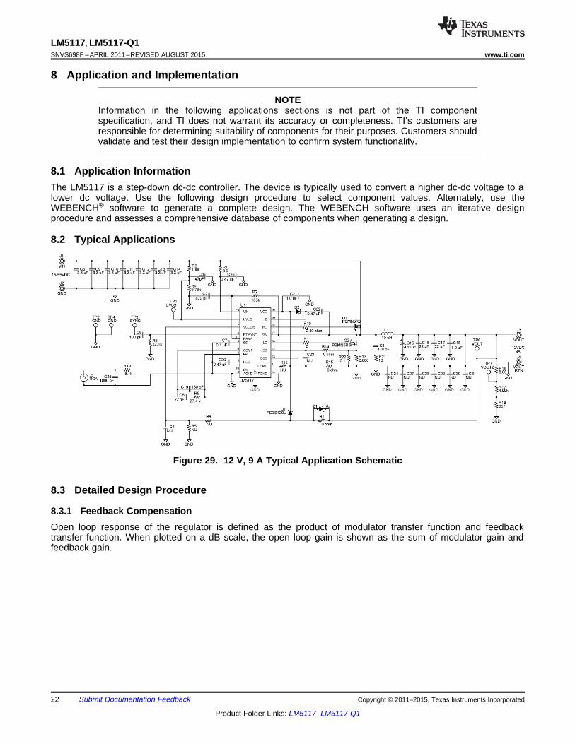
Figure 29. 12 V, 9 A Typical Application Schematic
8.3 Detailed Design Procedure
8.3.1 Feedback CompensationOpen loop response of the regulator is defined as the product of modulator transfer function and feedbacktransfer function. When plotted on a dB scale, the open loop gain is shown as the sum of modulator gain andfeedback gain.
22 Submit Documentation Feedback Copyright © 2011–2015, Texas Instruments Incorporated
Product Folder Links: LM5117 LM5117-Q1

K - 0.5
fSWZp_HF =
2 x ' x RS x RFB2 x AS x COUT
RCOMPfCROSS = [Hz]
RFB2 x (CCOMP + CHF)1
Where AFB (Feedback DC gain) = ,
RCOMP x CCOMP
1wZ_EA (Low frequency zero) = ,
RCOMP x CHF
1wP_EA (High frequency pole) =
=s
AFB x
ZP_EAVOUT^
VCOMP^
-ZZ_EA
1 + s
s x (1+ )
1RLOAD x COUT
ZP_LF (Load pole) =
ZZ_ESR (ESR zero) =1
RESR x COUT,
RLOAD
RS x ASWhere AM (Modulator DC gain) = ,
ZZ_ESR1 +
VOUT
VCOMP
= AM x
s
1+s
ZP_LF©§
¹·
^
^
LM5117, LM5117-Q1www.ti.com SNVS698F –APRIL 2011–REVISED AUGUST 2015
Detailed Design Procedure (continued)The modulator transfer function includes a power stage transfer function with an embedded current loop and canbe simplified as one pole and one zero system as shown in Equation 15.
(15)
If the ESR of COUT (RESR) is very small, the modulator transfer function can be further simplified to a one polesystem and the voltage loop can be closed with only two loop compensation components, RCOMP and CCOMP,leaving a single pole response at the crossover frequency. A single pole response at the crossover frequencyyields a very stable loop with 90 degrees of phase margin.
The feedback transfer function includes the feedback resistor divider and loop compensation of the erroramplifier. RCOMP, CCOMP and optional CHF configure the error amplifier gain and phase characteristics and createa pole at origin, a low frequency zero and a high frequency pole. This is shown mathematically in Equation 16.
(16)
The pole at the origin minimizes output steady state error. The low frequency zero should be placed to cancel theload pole of the modulator. The high frequency pole can be used to cancel the zero created by the outputcapacitor ESR or to decrease noise susceptibility of the error amplifier. By placing the low frequency zero anorder of magnitude less than the crossover frequency, the maximum amount of phase boost can be achieved atthe crossover frequency. The high frequency pole should be placed well beyond the crossover frequency sincethe addition of CHF adds a pole in the feedback transfer function.
The crossover frequency (loop bandwidth) is usually selected between one twentieth and one fifth of the fSW. In asimplified formula, the crossover frequency can be defined as:
(17)
For higher crossover frequency, RCOMP can be increased, while proportionally decreasing CCOMP. Conversely,decreasing RCOMP while proportionally increasing CCOMP, results in lower bandwidth while keeping the same zerofrequency in the feedback transfer function.
The sampled gain inductor pole is inversely proportional to the K factor, which is defined as:
(18)
Copyright © 2011–2015, Texas Instruments Incorporated Submit Documentation Feedback 23
Product Folder Links: LM5117 LM5117-Q1
= 1 - K1
dl0dl1
Steady-State Inductor Current
dI0
dI1tON
Inductor Current with Initial Perturbation
LM5117, LM5117-Q1SNVS698F –APRIL 2011–REVISED AUGUST 2015 www.ti.com
Detailed Design Procedure (continued)The maximum achievable loop bandwidth, in fact, is limited by this sampled gain inductor pole. In traditionalcurrent mode control, the maximum achievable loop bandwidth varies with input voltage. With the LM5117’sunique slope compensation scheme, the sampled gain inductor pole is independent of changes to the inputvoltage. This frees the user from additional concerns in wide varying input range applications and is anadvantage of the LM5117.
If the sampled gain inductor pole or the ESR zero is close to the crossover frequency, it is recommended that thecomprehensive formulas in Table 1 be used and the stability should be checked by a network analyzer. Themodulator transfer function can be measured and the feedback transfer function can be configured for thedesired open loop transfer function. If a network analyzer is not available, step load transient tests can beperformed to verify acceptable performance. The step load goal is minimum overshoot/undershoot with adamped response.
8.3.2 Sub-Harmonic OscillationPeak current mode regulators can exhibit unstable behavior when operating above 50% duty cycle. Thisbehavior is known as sub-harmonic oscillation and is characterized by alternating wide and narrow pulses at theSW pin. Sub-harmonic oscillation can be prevented by adding an additional voltage ramp (slope compensation)on top of the sensed inductor current shown in Figure 20. By choosing K≥1, the regulator will not be subject tosub-harmonic oscillation caused by a varying input voltage.
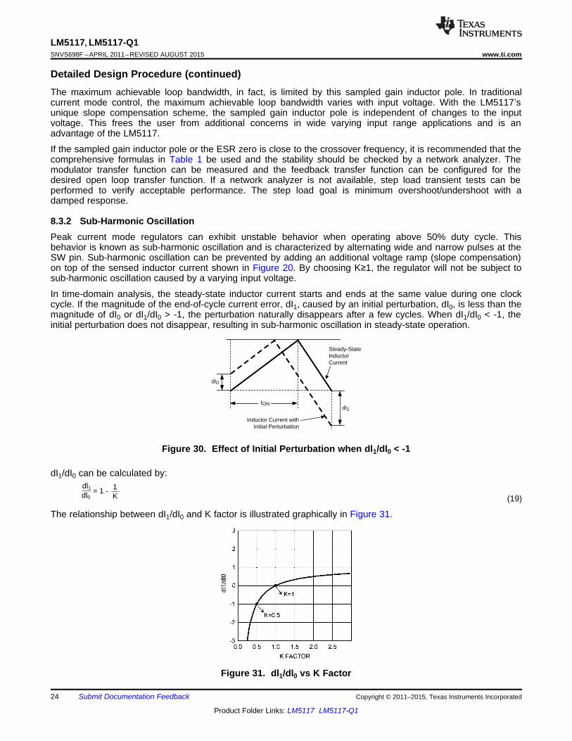
In time-domain analysis, the steady-state inductor current starts and ends at the same value during one clockcycle. If the magnitude of the end-of-cycle current error, dI1, caused by an initial perturbation, dI0, is less than themagnitude of dI0 or dI1/dI0 > -1, the perturbation naturally disappears after a few cycles. When dI1/dI0 < -1, theinitial perturbation does not disappear, resulting in sub-harmonic oscillation in steady-state operation.
Figure 30. Effect of Initial Perturbation when dl1/dl0 < -1
dI1/dI0 can be calculated by:
(19)
The relationship between dI1/dI0 and K factor is illustrated graphically in Figure 31.
Figure 31. dl1/dl0 vs K Factor
24 Submit Documentation Feedback Copyright © 2011–2015, Texas Instruments Incorporated
Product Folder Links: LM5117 LM5117-Q1
5.2 x 10⁹
RT =230 x 103 - 948 = 21.7 k:
1S(K-0.5)
Q =
LM5117, LM5117-Q1www.ti.com SNVS698F –APRIL 2011–REVISED AUGUST 2015
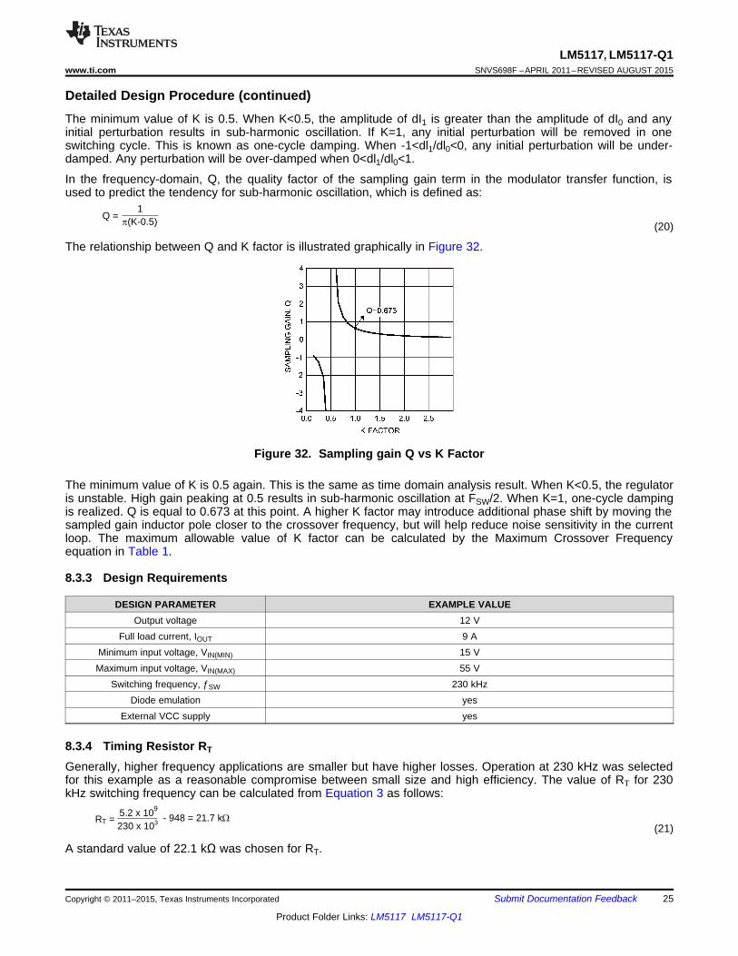
Detailed Design Procedure (continued)The minimum value of K is 0.5. When K<0.5, the amplitude of dI1 is greater than the amplitude of dI0 and anyinitial perturbation results in sub-harmonic oscillation. If K=1, any initial perturbation will be removed in oneswitching cycle. This is known as one-cycle damping. When -1<dl1/dl0<0, any initial perturbation will be under-damped. Any perturbation will be over-damped when 0<dl1/dl0<1.
In the frequency-domain, Q, the quality factor of the sampling gain term in the modulator transfer function, isused to predict the tendency for sub-harmonic oscillation, which is defined as:
(20)
The relationship between Q and K factor is illustrated graphically in Figure 32.
Figure 32. Sampling gain Q vs K Factor
The minimum value of K is 0.5 again. This is the same as time domain analysis result. When K<0.5, the regulatoris unstable. High gain peaking at 0.5 results in sub-harmonic oscillation at FSW/2. When K=1, one-cycle dampingis realized. Q is equal to 0.673 at this point. A higher K factor may introduce additional phase shift by moving thesampled gain inductor pole closer to the crossover frequency, but will help reduce noise sensitivity in the currentloop. The maximum allowable value of K factor can be calculated by the Maximum Crossover Frequencyequation in Table 1.
8.3.3 Design Requirements
DESIGN PARAMETER EXAMPLE VALUEOutput voltage 12 V
Full load current, IOUT 9 AMinimum input voltage, VIN(MIN) 15 VMaximum input voltage, VIN(MAX) 55 V
Switching frequency, ƒSW 230 kHzDiode emulation yes
External VCC supply yes
8.3.4 Timing Resistor RT
Generally, higher frequency applications are smaller but have higher losses. Operation at 230 kHz was selectedfor this example as a reasonable compromise between small size and high efficiency. The value of RT for 230kHz switching frequency can be calculated from Equation 3 as follows:
(21)
A standard value of 22.1 kΩ was chosen for RT.
Copyright © 2011–2015, Texas Instruments Incorporated Submit Documentation Feedback 25
Product Folder Links: LM5117 LM5117-Q1
7.41 m: 10 PH55V x 100 ns
+ILIM_PK =0.12V
= 16.7A
¹·
©§
55VPRS = 1 - x 9A2 x 7.41 m: = 0.47W
12V
¸¹
ᬩ
§VIN(MAX)
PRS = 1 - IOUT2 x RS
VOUT x [W]
9A x 1.3 +230 kHz x 10 µH
12 x 1RS =
0.12V= 7.3 m:
1.04A_2
RS =VCS(TH)
>:@
IOUT(MAX) + fSW x LO
VOUT x K IPP
2_
¸¹·
¨©§
55VIPP(MAX) = x 1 -12V12V
10 PH x 230 kHz= 4.1A
( )
OUT OUTO
PP(MAX) SW IN MAX
V V 12V 12VL 1 1 11.3 H
I f V 9 A 0.4 230kHz 55 V
æ ö æ öç ÷= ´ - = ´ - = mç ÷ç ÷´ ´ ´ è øè ø
LM5117, LM5117-Q1SNVS698F –APRIL 2011–REVISED AUGUST 2015 www.ti.com
8.3.5 Output Inductor LO
The maximum inductor ripple current occurs at the maximum input voltage. Typically, 20% to 40% of the full loadcurrent is a good compromise between core loss and copper loss of the inductor. Higher ripple current allows fora smaller inductor size, but places more of a burden on the output capacitor to smooth the ripple voltage on theoutput. For this example, a ripple current of 40% of 9 A was chosen. Knowing the switching frequency, maximumripple current, maximum input voltage and the nominal output voltage, the inductor value can be calculated asfollows:
(22)
The closest standard value of 10 μH was chosen for LO. Using the value of 10 μH for LO, calculate IPP again.This step is necessary if the chosen value of LO differs significantly from the calculated value.
From Equation 11,
(23)
At the minimum input voltage, this value is 1.04 A.
8.3.6 Diode Emulation FunctionThe DEMB pin is left floating since this example uses diode emulation to reduce the power loss under no load orlight load conditions.
8.3.7 Current Sense Resistor RS
The performance of the converter will vary depending on the K value. For this example, K = 1 was chosen tocontrol sub-harmonic oscillation and achieve one-cycle damping. The maximum output current capability(IOUT(MAX)) should be 20~50% higher than the required output current, to account for tolerances and ripplecurrent. For this example, 130% of 9 A was chosen. The current sense resistor value can be calculated fromEquation 9 and Equation 10 as follows:
(24)
(25)
A value of 7.41 mΩ was realized for RS by placing an additional 0.1-Ω sense resistor in parallel with 8 mΩ. Thesense resistor must be rated to handle the power dissipation at maximum input voltage when current flowsthrough the low-side NMOS for the majority of the PWM cycle. The maximum power dissipation of RS can becalculated as:
(26)
(27)
The worst case peak inductor current under the output short condition can be calculated from Equation 12 asfollows:
where• tON(MIN) is normally 100ns (28)
26 Submit Documentation Feedback Copyright © 2011–2015, Texas Instruments Incorporated
Product Folder Links: LM5117 LM5117-Q1

PDC (Low-Side) = (1 ± D) x (IOUT2 x RDS(ON) x 1.3) [W]
PDC (High-Side) = D x (IOUT2 x RDS(ON) x 1.3) [W]
1.25V x 100 k:14V -1.25V
RUV1 = = 9.8 k:
2V20 µA
RUV2 = = 100 k:
10 PH1 x 820 pF x 7.41 m:x 10
RRAMP = = 165 k:
LO
K x CRAMP x RSx ASRRAMP = [:@
LM5117, LM5117-Q1www.ti.com SNVS698F –APRIL 2011–REVISED AUGUST 2015
8.3.8 Current Sense Filter RCS and CCS
The LM5117 itself is not affected by the large leading edge spike because it samples valley current just prior tothe onset of the high-side switch. A current sense filter is used to minimize a noise injection from any externalnoise sources. In general, a current sense filter is not necessary. In this example, a current sense filter is notused
Adding RCS resistor changes the current sense amplifier gain which is defined as AS=10 k / (1 k+RCS). A smallvalue of RCS resistor below 100 Ω is recommended to minimize the gain change which is caused by thetemperature coefficient difference between internal and external resistors.
8.3.9 Ramp Resistor RRAMP and Ramp Capacitor CRAMP
The positive slope of the inductor current ramp signal is emulated by RRAMP and CRAMP. For this example, thevalue of CRAMP was set at the standard capacitor value of 820 pF. With the inductor, sense resistor and the Kfactor selected, the value of RRAMP can be calculated from Equation 4 as follows:
(29)
(30)
The standard value of 165 kΩ was selected for RRAMP.
8.3.10 UVLO Divider RUV2, RUV1 and CFT
The desired startup voltage and the hysteresis are set by the voltage divider RUV1 and RUV2. Capacitor CFTprovides filtering for the divider. For this design, the startup voltage was set to 14 V, 1 V below VIN(MIN). VHYS wasset to 2 V. The value of RUV1, RUV2 can be calculated from Equation 1 and Equation 2 as follows:
(31)
(32)
The standard value of 100 kΩ was selected for RUV2. RUV1 was selected to be 9.76 kΩ. A value of 47 pF waschosen for CFT.
8.3.11 VCC Disable and External VCC SupplyThe 12-V output voltage allows the external VCC supply configuration as shown in Figure 16. In this example,VCCDIS can be left floating since VOUT is higher than VCC regulator set-point level.
8.3.12 Power Switches QH and QL
Selection of the power NMOS devices is governed by the same trade-offs as switching frequency. Breakingdown the losses in the high-side and low-side NMOS devices is one way to compare the relative efficiencies ofdifferent devices. Losses in the power NMOS devices can be broken down into conduction loss, gate chargingloss, and switching loss.
Conduction loss PDC is approximately:
(33)
where• D is the duty cycle• the factor of 1.3 accounts for the increase in the NMOS device on-resistance due to heating (34)
Alternatively, the factor of 1.3 can be eliminated and the high temperature on-resistance of the NMOS device canbe estimated using the RDS(ON) vs Temperature curves in the MOSFET datasheet.
Copyright © 2011–2015, Texas Instruments Incorporated Submit Documentation Feedback 27
Product Folder Links: LM5117 LM5117-Q1
CHB Qg
'VHBt [F]
PSW = 0.5 x VIN x IOUT x (tR + tF) x fSW [W]
PGC = n x VVCC x Qg x fSW [W]
LM5117, LM5117-Q1SNVS698F –APRIL 2011–REVISED AUGUST 2015 www.ti.com
Gate charging loss (PGC) results from the current driving the gate capacitance of the power NMOS devices and isapproximated as:
(35)
Qg refers to the total gate charge of an individual NMOS device, and ‘n’ is the number of NMOS devices. Gatecharge loss differs from conduction and switching losses in that the actual dissipation occurs in the controller IC.Switching loss (PSW) occurs during the brief transition period as the high-side NMOS device turns on and off.During the transition period both current and voltage are present in the channel of the NMOS device. Theswitching loss can be approximated as:
(36)
tR and tF are the rise and fall times of the high-side NMOS device. The rise and fall times are usually mentionedin the MOSFET datasheet or can be empirically observed with an oscilloscope. Switching loss is calculated forthe high-side NMOS device only. Switching loss in the low-side NMOS device is negligible because the bodydiode of the low-side NMOS device turns on before and after the low-side NMOS device switches. For thisexample, the maximum drain-to-source voltage applied to either NMOS device is 55 V. The selected NMOSdevices must be able to withstand 55 V plus any ringing from drain to source and must be able to handle at leastthe VCC voltage plus any ringing from gate to source.
8.3.13 Snubber Components RSNB and CSNB
A resistor-capacitor snubber network across the low-side NMOS device reduces ringing and spikes at theswitching node. Excessive ringing and spikes can cause erratic operation and can couple noise to the outputvoltage. Selecting the values for the snubber is best accomplished through empirical methods. First, make surethe lead lengths for the snubber connections are very short. Start with a resistor value between 5 and 50 Ω.Increasing the value of the snubber capacitor results in more damping, but higher snubber losses. Select aminimum value for the snubber capacitor that provides adequate damping of the spikes on the switch waveformat heavy load. A snubber may not be necessary with an optimized layout.
8.3.14 Bootstrap Capacitor CHB and Bootstrap Diode DHB
The bootstrap capacitor between the HB and SW pin supplies the gate current to charge the high-side NMOSdevice gate during each cycle’s turn-on and also supplies recovery charge for the bootstrap diode. These currentpeaks can be several amperes. The recommended value of the bootstrap capacitor is at least 0.1 μF. CHB shouldbe a good quality, low ESR, ceramic capacitor located at the pins of the IC to minimize potentially damagingvoltage transients caused by trace inductance. The absolute minimum value for the bootstrap capacitor iscalculated as:
where• Qg is the high-side NMOS gate charge• ΔVHB is the tolerable voltage droop on CHB, which is typically less than 5% of VCC or 0.15 V conservatively
(37)
A value of 0.47 μF was selected for this design.
8.3.15 VCC Capacitor CVCC
The primary purpose of the VCC capacitor (CVCC) is to supply the peak transient currents of the LO driver andbootstrap diode as well as provide stability for the VCC regulator. These peak currents can be several amperes.The recommended value of CVCC should be no smaller than 0.47μF, and should be a good quality, low ESR,ceramic capacitor. CVCC should be placed at the pins of the IC to minimize potentially damaging voltagetransients caused by trace inductance. A value of 1 μF was selected for this design.
28 Submit Documentation Feedback Copyright © 2011–2015, Texas Instruments Incorporated
Product Folder Links: LM5117 LM5117-Q1

tRES 0.47 µF x 1.25V
10 µA= = 59 ms
0.1 µF x 0.8VtSS =
10 µA= 8 ms
'VIN =4 x 230 kHz x 3.3 PFx 7
9 A= 0.42 V
'VIN =4 x x CIN fSW
IOUT[V]
12
¸¹·
¨©§8 x 230 kHz x 470 PF
'VOUT = 4.1 x 0.02:2 + =82 mV
12
¸¹
ᬩ
§8 x x COUT fSW
'VOUT = IPP x RESR2 + [V]
LM5117, LM5117-Q1www.ti.com SNVS698F –APRIL 2011–REVISED AUGUST 2015
8.3.16 Output Capacitor CO
The output capacitors smooth the output voltage ripple caused by inductor ripple current and provide a source ofcharge during transient loading conditions. For this design example, a 470-μF electrolytic capacitor withmaximum 20mΩ ESR was selected as the main output capacitor. The fundamental component of the outputripple voltage with maximum ESR is approximated as:
(38)
(39)
Additional low ERS / ESL ceramic capacitors can be placed in parallel with the main output capacitor to furtherreduce the output voltage ripple and spikes. In this example, two 22μF capacitors were added.
8.3.17 Input Capacitor CIN
The regulator input supply voltage typically has high source impedance at the switching frequency. Good qualityinput capacitors are necessary to limit the ripple voltage at the VIN pin while supplying most of the switch currentduring the on-time. When the high-side NMOS device turns on, the current into the device steps to the valley ofthe inductor current waveform, ramps up to the peak value, and then drops to the zero at turnoff. The inputcapacitor should be selected for RMS current rating and minimum ripple voltage. A good approximation for therequired ripple current rating necessary is IRMS > IOUT / 2.
In this example, seven 3.3μF ceramic capacitors were used. With ceramic capacitors, the input ripple voltage willbe triangular. The input ripple voltage can be approximated as:
(40)
(41)
Capacitors connected in parallel should be evaluated for RMS current rating. The current will split between theinput capacitors based on the relative impedance of the capacitors at the switching frequency.
8.3.18 VIN Filter RVIN, CVIN
An R-C filter (RVIN, CVIN) on VIN is optional. The filter helps to prevent faults caused by high frequency switchingnoise injection into the VIN pin. A 0.47-μF ceramic capacitor is used for CVIN in the example. RVIN is selected tobe 3.9 Ω.
8.3.19 Soft-Start Capacitor CSS
The capacitor at the SS pin (CSS) determines the soft-start time (tSS), which is the time for the output voltage toreach the final regulated value. The tSS for a given CSS can be calculated from Equation 8 as follows:
(42)
For this example, a value of 0.1 μF was chosen for a soft-start time of 8 ms.
8.3.20 Restart Capacitor CRES
The capacitor at the RES pin (CRES) determines tRES, which is the time the LM5117 remains off before a restartattempt is made in hiccup mode current limiting. tRES for a given CRES can be calculated from Equation 13 asfollows:
(43)
For this example, a value of 0.47 μF was chosen for a restart time of 59 ms.
Copyright © 2011–2015, Texas Instruments Incorporated Submit Documentation Feedback 29
Product Folder Links: LM5117 LM5117-Q1
CHF 10 m: x 514 µF x 22 nF
27.4k: x 22 nF - 10 m: x 514 µF= = 189 pF
CHF RESR x COUT x CCOMP
RCOMP x CCOMP - RESR x COUT= [F]
LOAD OUTCOMP
COMP
12V514 F
9 AR CC 25nF
R 27.4k
æ ö´ mç ÷´ è ø= = =
W
RCOMP = 2Sx 7.41 m: x 10 x 514 µF x 4.99 k: x 23 kHz = 27.5 k:
RCOMP = 2Sx RS x AS x COUT x RFB2 x fCROSS [:@
10fCROSS = = 23 kHzfSW
RFB2- 1
RFB1
VOUT
0.8V=
LM5117, LM5117-Q1SNVS698F –APRIL 2011–REVISED AUGUST 2015 www.ti.com
8.3.21 Output Voltage Divider RFB2 and RFB1
RFB1 and RFB2 set the output voltage level. The ratio of these resistors is calculated as:
(44)
The ratio between RCOMP and RFB2 determines the mid-band gain, AFB_MID. A larger value for RFB2 may require acorresponding larger value for RCOMP. RFB2 should be large enough to keep the total divider power dissipationsmall. 4.99 kΩ was chosen for RFB2 in this example, which results in a RFB1 value of 357 Ω for 12-V output.
8.3.22 Loop Compensation Components CCOMP, RCOMP and CHF
RCOMP, CCOMP and CHF configure the error amplifier gain and phase characteristics to produce a stable voltageloop. For a quick start, follow the 4 steps listed below.
STEP1: Select fCROSS
By selecting one tenth of the switching frequency, fCROSS is calculated as follows:
(45)
STEP2: Determine required RCOMP
Knowing fCROSS, RCOMP is calculated as follows:
(46)
(47)
The standard value of 27.4kΩ was selected for RCOMP
STEP3: Determine CCOMP to cancel load poleKnowing RCOMP, CCOMP is calculated as follows:
(48)
The standard value of 22nF was selected for CCOMP
STEP4: Determine CHF to cancel ESR zeroKnowing RCOMP and CCOMP, CHF is calculated as follows:
(49)
(50)
Half of the maximum ESR is assumed as a typical ESR. The standard value of 180pF was selected for CHF.
30 Submit Documentation Feedback Copyright © 2011–2015, Texas Instruments Incorporated
Product Folder Links: LM5117 LM5117-Q1
1 ZP_EA =
RCOMP x CHF
1 ZP_EA =
RCOMP x (CHF // CCOMP )
ZZ_EA = RCOMP x CCOMP 1
ZZ_EA = RCOMP x CCOMP 1
AFB_MID =RCOMP
RFB2AFB_MID =
RCOMP
RFB2
AFB =1
RFB2 x (CCOMP + CHF)AFB =
1RFB2 x (CCOMP + CHF)
=s
AFB x
ZP_EAVOUT^
VCOMP^
-ZZ_EA
1 + s
s x (1+ ) =
sAFB x
ZP_EAVOUT^
VCOMP^
-ZZ_EA
1 + s
s x (1+ )
K = 1 K = LO
RRAMP x CRAMP x RS x AS
2
fSWZn =
ZSW
2=Sx fSW or fn =
Q = 1
S(K - 0.5)
ZP_HF Q x Zn =ZP_HFfSW
K 0.5 = or
ZP_LF = RLOAD x COUT
1 ZP_LF =
(RLOAD + RESR1) x (COUT1 + COUT2) LO x (COUT1 + COUT2) x ZP_HF
1 1 +
RESR1
1 ZP_ESR =
x (COUT1 // COUT2 )
ZZ_ESR =RESR
1 x COUT
ZZ_ESR =RESR1
1 x COUT1
AM =RLOAD
RS x AS x LO ZP_HF
x1
1 + RLOADAM =
RLOAD
RS x AS
=VOUT^
VCOMP^
AM xZZ_ESR
1 + s
s(1 + ) ZP_LF
x (1 + ) ZP_ESR
x (1 + + ) s sZP_HF
s2
Zn2(1 + )
ZZ_ESR=
sVOUT^
VCOMP^ AM x
ZP_LF
1 + s
LM5117, LM5117-Q1www.ti.com SNVS698F –APRIL 2011–REVISED AUGUST 2015
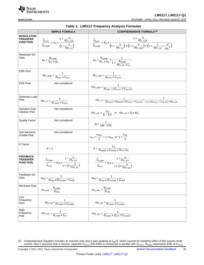
Table 1. LM5117 Frequency Analysis FormulasSIMPLE FORMULA COMPREHENSIVE FORMULA (1)
MODULATORTRANSFERFUNCTION
Modulator DCGain
ESR Zero
ESR Pole Not considered
Dominant LoadPole
Sampled Gain Not consideredInductor Pole
Quality Factor Not considered
Sub-harmonic Not consideredDouble Pole
K Factor
FEEDBACKTRANSFERFUNCTION
Feedback DCGain
Mid-band Gain
LowFrequencyZero
HighFrequencyPole
(1) Comprehensive Equation includes an inductor pole and a gain peaking at fSW/2, which caused by sampling effect of the current modecontrol. Also it assumes that a ceramic capacitor COUT2 (No ESR) is connected in parallel with COUT1. RESR1 represents ESR of COUT1 .
Copyright © 2011–2015, Texas Instruments Incorporated Submit Documentation Feedback 31
Product Folder Links: LM5117 LM5117-Q1

fCROSS_MAX = fSW
4 x Q1 + 4 x Q2 -1 x ( ) fCROSS_MAX =
fSW
5
ZP_EA = ZZ_ESRZZ_EA = ZP_LFwhen &
fCROSS < ZP_HF
2 x S x 10& & fCROSS < ZP_ESR
2 x S x 10
ZP_EA = ZZ_ESRZZ_EA = ZP_LF &when
2 x ' x RS x RFB2 x AS x COUT
RCOMPfCROSS =
2 x ' x RS x RFB2 x AS x (COUT1 + COUT2)
RCOMPfCROSS =
ZZ_EA = ZP_LFwhen
ZP_EA = ZZ_ESRZZ_EA = ZP_LF &when
T(s) = s
AM x AFB x
ZZ_ESR1 + s
s(1 + ) ZP_EA
x (1 + ) ZP_ESR
x (1 + + ) s sZP_HF
s2
Zn2
T(s) AM x AFB
s=
T(s) = AM x AFB x xZZ_ESR
1 + s
s(1 + ) ZP_LF
x (1 + ) ZP_ESR
x (1 + + ) s sZP_HF
s2
Zn2
s(1 + ) ZP_EA
s x
ZZ_EA1 + s
T(s) = AM x AFB xZZ_EA
s(1 + ) ZP_EA
1 + s
s x s(1 + ) ZP_LF
xZZ_ESR
1 + s
LM5117, LM5117-Q1SNVS698F –APRIL 2011–REVISED AUGUST 2015 www.ti.com
Table 1. LM5117 Frequency Analysis Formulas (continued)SIMPLE FORMULA COMPREHENSIVE FORMULA (1)
OPEN-LOOPRESPONSE
Cross OverFrequency(Open LoopBandwidth)
MaximumCross OverFrequency
The frequency at which 45° phase shift occurs in modulator phasecharacteristics.
8.4 Application Curves
Figure 34. Typical Efficiency vs Load CurrentFigure 33. Start-Up with Resistive Load
32 Submit Documentation Feedback Copyright © 2011–2015, Texas Instruments Incorporated
Product Folder Links: LM5117 LM5117-Q1

VOUT
SS
RES
RT
COMP
FB
RAMP
PGND
CSG
CS
LO
SW
HO
HB
VCCVIN
AGND
UVLO
VCCDIS
DEMB
CM
VIN
VOUT
SW
LM5117
CIN
QH
QL
CHB
DHB
CVCC
Hiccup Mode OVPTriggered at 13.4V
CC Mode: 2A
100k:
15 k:
80 µF
68 µH1500 pF
100 k:
22.1 k:0.47 µF
3.24 k:
2.37 k:
0.022 µF
47 m:
Current Control (CC)
3.24 k:
332:
LM5117, LM5117-Q1www.ti.com SNVS698F –APRIL 2011–REVISED AUGUST 2015
Application Curves (continued)8.4.1 Constant Current RegulatorThe LM5117 can be configured as a constant current regulator by using the current monitor feature (CM) as thefeedback input. A voltage divider at the VCCDIS pin from VOUT to AGND can be used to protect against outputover-voltage. When the VCCDIS pin voltage is greater than the VCCDIS threshold, the controller disables theVCC regulator and the VCC pin voltage decays. When the VCC pin voltage is less than the VCC UV threshold,both HO and LO outputs stop switching. Due to the time delay required for VCC to decay below the VCC UVthreshold, the over-voltage protection operates in hiccup mode. See Figure 35.
Figure 35. Constant Current Regulator With Hiccup Mode Output OVP
8.4.2 Constant Voltage and Constant Current RegulatorThe LM5117 also can be configured as a constant voltage and constant current regulator, known as CV+CCregulator. In this configuration, there is much less variation in the current limiting as compared to peak cycle-by-cycle current limiting of the inductor current. The LMV431 and the PNP transistor create a voltage-to-currentamplifier in the current loop. This amplifier circuitry does not affect the normal operation when the output currentis less than the current limit set-point. When the output current is greater than the set-point, the PNP transistorsources a current into CRAMP and increases the positive slope of emulated inductor current ramp until the outputcurrent is less than or equal to the current limit set-point. See Figure 36 and Figure 37.
Copyright © 2011–2015, Texas Instruments Incorporated Submit Documentation Feedback 33
Product Folder Links: LM5117 LM5117-Q1

VOUT
SS
RES
RT
COMP
FB
RAMP
PGND
CSG
CS
LO
SW
HO
HB
VCCVIN
AGND
UVLO
VCCDIS
DEMB
CM
VIN
VOUT
SW
LM5117
CIN
QH
QL
Current Control (CC)
CHB
DHB
CVCC
VCC
Voltage Control (CV)
LMV431
CV Mode : 5VCC Mode: 2A
100 k:
15 k:
80 PF
68 PH1500 pF
100 k:
22.1 k:0.33 PF x2
3.24 k:
619:
34.8 k:0.1 PF
47 m:
1 nF
100 k:
10 k: 100:
PNP
200 k:
LM5117, LM5117-Q1SNVS698F –APRIL 2011–REVISED AUGUST 2015 www.ti.com
Application Curves (continued)
Figure 36. Constant Voltage Regulator with Accurate Current Limit
Figure 37. Current Limit Comparison
34 Submit Documentation Feedback Copyright © 2011–2015, Texas Instruments Incorporated
Product Folder Links: LM5117 LM5117-Q1
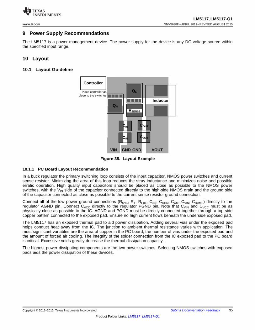
Controller
VOUTGNDGNDVIN
Inductor
CIN
CIN
COUT
COUT
RSENSE
QH
QLPlace controller as close to the switches
LM5117, LM5117-Q1www.ti.com SNVS698F –APRIL 2011–REVISED AUGUST 2015
9 Power Supply RecommendationsThe LM5117 is a power management device. The power supply for the device is any DC voltage source withinthe specified input range.
10 Layout
10.1 Layout Guideline
Figure 38. Layout Example
10.1.1 PC Board Layout RecommendationIn a buck regulator the primary switching loop consists of the input capacitor, NMOS power switches and currentsense resistor. Minimizing the area of this loop reduces the stray inductance and minimizes noise and possibleerratic operation. High quality input capacitors should be placed as close as possible to the NMOS powerswitches, with the VIN side of the capacitor connected directly to the high-side NMOS drain and the ground sideof the capacitor connected as close as possible to the current sense resistor ground connection.
Connect all of the low power ground connections (RUV1, RT, RFB1, CSS, CRES, CCM, CVIN, CRAMP) directly to theregulator AGND pin. Connect CVCC directly to the regulator PGND pin. Note that CVIN and CVCC must be asphysically close as possible to the IC. AGND and PGND must be directly connected together through a top-sidecopper pattern connected to the exposed pad. Ensure no high current flows beneath the underside exposed pad.
The LM5117 has an exposed thermal pad to aid power dissipation. Adding several vias under the exposed padhelps conduct heat away from the IC. The junction to ambient thermal resistance varies with application. Themost significant variables are the area of copper in the PC board, the number of vias under the exposed pad andthe amount of forced air cooling. The integrity of the solder connection from the IC exposed pad to the PC boardis critical. Excessive voids greatly decrease the thermal dissipation capacity.
The highest power dissipating components are the two power switches. Selecting NMOS switches with exposedpads aids the power dissipation of these devices.
Copyright © 2011–2015, Texas Instruments Incorporated Submit Documentation Feedback 35
Product Folder Links: LM5117 LM5117-Q1
LM5117, LM5117-Q1SNVS698F –APRIL 2011–REVISED AUGUST 2015 www.ti.com
11 Device and Documentation Support
11.1 Related LinksThe table below lists quick access links. Categories include technical documents, support and communityresources, tools and software, and quick access to sample or buy.
Table 2. Related LinksTECHNICAL TOOLS & SUPPORT &PARTS PRODUCT FOLDER SAMPLE & BUY DOCUMENTS SOFTWARE COMMUNITY
LM5117 Click here Click here Click here Click here Click hereLM5117-Q1 Click here Click here Click here Click here Click here
11.2 Community ResourcesThe following links connect to TI community resources. Linked contents are provided "AS IS" by the respectivecontributors. They do not constitute TI specifications and do not necessarily reflect TI's views; see TI's Terms ofUse.
TI E2E™ Online Community TI's Engineer-to-Engineer (E2E) Community. Created to foster collaborationamong engineers. At e2e.ti.com, you can ask questions, share knowledge, explore ideas and helpsolve problems with fellow engineers.
Design Support TI's Design Support Quickly find helpful E2E forums along with design support tools andcontact information for technical support.
11.3 TrademarksE2E is a trademark of Texas Instruments.WEBENCH is a registered trademark of Texas Instruments.All other trademarks are the property of their respective owners.
11.4 Electrostatic Discharge CautionThese devices have limited built-in ESD protection. The leads should be shorted together or the device placed in conductive foamduring storage or handling to prevent electrostatic damage to the MOS gates.
11.5 GlossarySLYZ022 — TI Glossary.
This glossary lists and explains terms, acronyms, and definitions.
12 Mechanical, Packaging, and Orderable InformationThe following pages include mechanical, packaging, and orderable information. This information is the mostcurrent data available for the designated devices. This data is subject to change without notice and revision ofthis document. For browser-based versions of this data sheet, refer to the left-hand navigation.
36 Submit Documentation Feedback Copyright © 2011–2015, Texas Instruments Incorporated
Product Folder Links: LM5117 LM5117-Q1
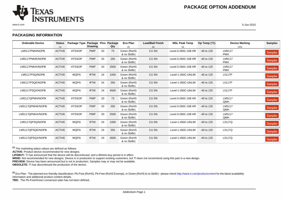
PACKAGE OPTION ADDENDUM
www.ti.com 5-Jun-2015
Addendum-Page 1
PACKAGING INFORMATION
Orderable Device Status(1)
Package Type PackageDrawing
Pins PackageQty
Eco Plan(2)
Lead/Ball Finish(6)
MSL Peak Temp(3)
Op Temp (°C) Device Marking(4/5)
Samples
LM5117PMH/NOPB ACTIVE HTSSOP PWP 20 73 Green (RoHS& no Sb/Br)
CU SN Level-3-260C-168 HR -40 to 125 LM5117PMH
LM5117PMHE/NOPB ACTIVE HTSSOP PWP 20 250 Green (RoHS& no Sb/Br)
CU SN Level-3-260C-168 HR -40 to 125 LM5117PMH
LM5117PMHX/NOPB ACTIVE HTSSOP PWP 20 2500 Green (RoHS& no Sb/Br)
CU SN Level-3-260C-168 HR -40 to 125 LM5117PMH
LM5117PSQ/NOPB ACTIVE WQFN RTW 24 1000 Green (RoHS& no Sb/Br)
CU SN Level-1-260C-UNLIM -40 to 125 L5117P
LM5117PSQE/NOPB ACTIVE WQFN RTW 24 250 Green (RoHS& no Sb/Br)
CU SN Level-1-260C-UNLIM -40 to 125 L5117P
LM5117PSQX/NOPB ACTIVE WQFN RTW 24 4500 Green (RoHS& no Sb/Br)
CU SN Level-1-260C-UNLIM -40 to 125 L5117P
LM5117QPMH/NOPB ACTIVE HTSSOP PWP 20 73 Green (RoHS& no Sb/Br)
CU SN Level-3-260C-168 HR -40 to 125 LM5117QMH
LM5117QPMHE/NOPB ACTIVE HTSSOP PWP 20 250 Green (RoHS& no Sb/Br)
CU SN Level-3-260C-168 HR -40 to 125 LM5117QMH
LM5117QPMHX/NOPB ACTIVE HTSSOP PWP 20 2500 Green (RoHS& no Sb/Br)
CU SN Level-3-260C-168 HR -40 to 125 LM5117QMH
LM5117QPSQ/NOPB ACTIVE WQFN RTW 24 1000 Green (RoHS& no Sb/Br)
CU SN Level-1-260C-UNLIM -40 to 125 L5117Q
LM5117QPSQE/NOPB ACTIVE WQFN RTW 24 250 Green (RoHS& no Sb/Br)
CU SN Level-1-260C-UNLIM -40 to 125 L5117Q
LM5117QPSQX/NOPB ACTIVE WQFN RTW 24 4500 Green (RoHS& no Sb/Br)
CU SN Level-1-260C-UNLIM -40 to 125 L5117Q
(1) The marketing status values are defined as follows:ACTIVE: Product device recommended for new designs.LIFEBUY: TI has announced that the device will be discontinued, and a lifetime-buy period is in effect.NRND: Not recommended for new designs. Device is in production to support existing customers, but TI does not recommend using this part in a new design.PREVIEW: Device has been announced but is not in production. Samples may or may not be available.OBSOLETE: TI has discontinued the production of the device.
(2) Eco Plan - The planned eco-friendly classification: Pb-Free (RoHS), Pb-Free (RoHS Exempt), or Green (RoHS & no Sb/Br) - please check http://www.ti.com/productcontent for the latest availabilityinformation and additional product content details.TBD: The Pb-Free/Green conversion plan has not been defined.
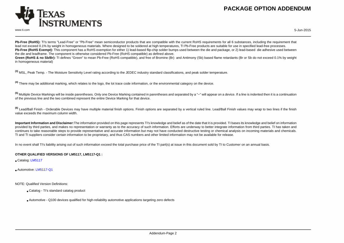
PACKAGE OPTION ADDENDUM
www.ti.com 5-Jun-2015
Addendum-Page 2
Pb-Free (RoHS): TI's terms "Lead-Free" or "Pb-Free" mean semiconductor products that are compatible with the current RoHS requirements for all 6 substances, including the requirement thatlead not exceed 0.1% by weight in homogeneous materials. Where designed to be soldered at high temperatures, TI Pb-Free products are suitable for use in specified lead-free processes.Pb-Free (RoHS Exempt): This component has a RoHS exemption for either 1) lead-based flip-chip solder bumps used between the die and package, or 2) lead-based die adhesive used betweenthe die and leadframe. The component is otherwise considered Pb-Free (RoHS compatible) as defined above.Green (RoHS & no Sb/Br): TI defines "Green" to mean Pb-Free (RoHS compatible), and free of Bromine (Br) and Antimony (Sb) based flame retardants (Br or Sb do not exceed 0.1% by weightin homogeneous material)
(3) MSL, Peak Temp. - The Moisture Sensitivity Level rating according to the JEDEC industry standard classifications, and peak solder temperature.
(4) There may be additional marking, which relates to the logo, the lot trace code information, or the environmental category on the device.
(5) Multiple Device Markings will be inside parentheses. Only one Device Marking contained in parentheses and separated by a "~" will appear on a device. If a line is indented then it is a continuationof the previous line and the two combined represent the entire Device Marking for that device.
(6) Lead/Ball Finish - Orderable Devices may have multiple material finish options. Finish options are separated by a vertical ruled line. Lead/Ball Finish values may wrap to two lines if the finishvalue exceeds the maximum column width.
Important Information and Disclaimer:The information provided on this page represents TI's knowledge and belief as of the date that it is provided. TI bases its knowledge and belief on informationprovided by third parties, and makes no representation or warranty as to the accuracy of such information. Efforts are underway to better integrate information from third parties. TI has taken andcontinues to take reasonable steps to provide representative and accurate information but may not have conducted destructive testing or chemical analysis on incoming materials and chemicals.TI and TI suppliers consider certain information to be proprietary, and thus CAS numbers and other limited information may not be available for release.
In no event shall TI's liability arising out of such information exceed the total purchase price of the TI part(s) at issue in this document sold by TI to Customer on an annual basis.
OTHER QUALIFIED VERSIONS OF LM5117, LM5117-Q1 :
• Catalog: LM5117
• Automotive: LM5117-Q1
NOTE: Qualified Version Definitions:
• Catalog - TI's standard catalog product
• Automotive - Q100 devices qualified for high-reliability automotive applications targeting zero defects

TAPE AND REEL INFORMATION
*All dimensions are nominal
Device PackageType
PackageDrawing
Pins SPQ ReelDiameter
(mm)
ReelWidth
W1 (mm)
A0(mm)
B0(mm)
K0(mm)
P1(mm)
W(mm)
Pin1Quadrant
LM5117PMHE/NOPB HTSSOP PWP 20 250 178.0 16.4 6.95 7.1 1.6 8.0 16.0 Q1
LM5117PMHX/NOPB HTSSOP PWP 20 2500 330.0 16.4 6.95 7.1 1.6 8.0 16.0 Q1
LM5117PSQ/NOPB WQFN RTW 24 1000 178.0 12.4 4.3 4.3 1.3 8.0 12.0 Q1
LM5117PSQE/NOPB WQFN RTW 24 250 178.0 12.4 4.3 4.3 1.3 8.0 12.0 Q1
LM5117PSQX/NOPB WQFN RTW 24 4500 330.0 12.4 4.3 4.3 1.3 8.0 12.0 Q1
LM5117QPMHE/NOPB HTSSOP PWP 20 250 178.0 16.4 6.95 7.1 1.6 8.0 16.0 Q1
LM5117QPMHX/NOPB HTSSOP PWP 20 2500 330.0 16.4 6.95 7.1 1.6 8.0 16.0 Q1
LM5117QPSQ/NOPB WQFN RTW 24 1000 178.0 12.4 4.3 4.3 1.3 8.0 12.0 Q1
LM5117QPSQE/NOPB WQFN RTW 24 250 178.0 12.4 4.3 4.3 1.3 8.0 12.0 Q1
LM5117QPSQX/NOPB WQFN RTW 24 4500 330.0 12.4 4.3 4.3 1.3 8.0 12.0 Q1
PACKAGE MATERIALS INFORMATION
www.ti.com 20-Sep-2016
Pack Materials-Page 1
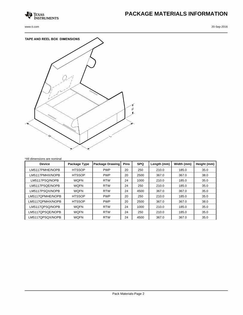
*All dimensions are nominal
Device Package Type Package Drawing Pins SPQ Length (mm) Width (mm) Height (mm)
LM5117PMHE/NOPB HTSSOP PWP 20 250 210.0 185.0 35.0
LM5117PMHX/NOPB HTSSOP PWP 20 2500 367.0 367.0 38.0
LM5117PSQ/NOPB WQFN RTW 24 1000 210.0 185.0 35.0
LM5117PSQE/NOPB WQFN RTW 24 250 210.0 185.0 35.0
LM5117PSQX/NOPB WQFN RTW 24 4500 367.0 367.0 35.0
LM5117QPMHE/NOPB HTSSOP PWP 20 250 210.0 185.0 35.0
LM5117QPMHX/NOPB HTSSOP PWP 20 2500 367.0 367.0 38.0
LM5117QPSQ/NOPB WQFN RTW 24 1000 210.0 185.0 35.0
LM5117QPSQE/NOPB WQFN RTW 24 250 210.0 185.0 35.0
LM5117QPSQX/NOPB WQFN RTW 24 4500 367.0 367.0 35.0
PACKAGE MATERIALS INFORMATION
www.ti.com 20-Sep-2016
Pack Materials-Page 2
www.ti.com
PACKAGE OUTLINE
C
24X 0.30.2
24X 0.50.3
0.8 MAX
(0.1) TYP
0.050.00
20X 0.5
2X2.5
2X 2.5
2.6 0.1
A 4.13.9
B
4.13.9
WQFN - 0.8 mm max heightRTW0024APLASTIC QUAD FLATPACK - NO LEAD
4222815/A 03/2016
PIN 1 INDEX AREA
0.08 C
SEATING PLANE
1
6 13
18
7 12
24 19(OPTIONAL)
PIN 1 ID 0.1 C A B0.05 C
EXPOSEDTHERMAL PAD
25
NOTES: 1. All linear dimensions are in millimeters. Any dimensions in parenthesis are for reference only. Dimensioning and tolerancing per ASME Y14.5M. 2. This drawing is subject to change without notice. 3. The package thermal pad must be soldered to the printed circuit board for thermal and mechanical performance.
SCALE 3.000

www.ti.com
EXAMPLE BOARD LAYOUT
0.07 MINALL AROUND
0.07 MAXALL AROUND
24X (0.25)
24X (0.6)
( ) TYPVIA
0.2
20X (0.5)(3.8)
(3.8)
(1.05)
( 2.6)
(R )TYP
0.05
(1.05)
WQFN - 0.8 mm max heightRTW0024APLASTIC QUAD FLATPACK - NO LEAD
4222815/A 03/2016
SYMM
1
6
7 12
13
18
1924
SYMM
LAND PATTERN EXAMPLESCALE:15X
25
NOTES: (continued) 4. This package is designed to be soldered to a thermal pad on the board. For more information, see Texas Instruments literature number SLUA271 (www.ti.com/lit/slua271).
SOLDER MASKOPENING
METAL UNDERSOLDER MASK
SOLDER MASKDEFINED
METAL
SOLDER MASKOPENING
SOLDER MASK DETAILS
NON SOLDER MASKDEFINED
(PREFERRED)

www.ti.com
EXAMPLE STENCIL DESIGN
24X (0.6)
24X (0.25)
20X (0.5)
(3.8)
(3.8)
4X ( 1.15)
(0.675)TYP
(0.675) TYP(R ) TYP0.05
WQFN - 0.8 mm max heightRTW0024APLASTIC QUAD FLATPACK - NO LEAD
4222815/A 03/2016
NOTES: (continued) 5. Laser cutting apertures with trapezoidal walls and rounded corners may offer better paste release. IPC-7525 may have alternate design recommendations.
SYMM
METALTYP
SOLDER PASTE EXAMPLEBASED ON 0.125 mm THICK STENCIL
EXPOSED PAD 25:
78% PRINTED SOLDER COVERAGE BY AREA UNDER PACKAGESCALE:20X
SYMM
1
6
7 12
13
18
1924
25
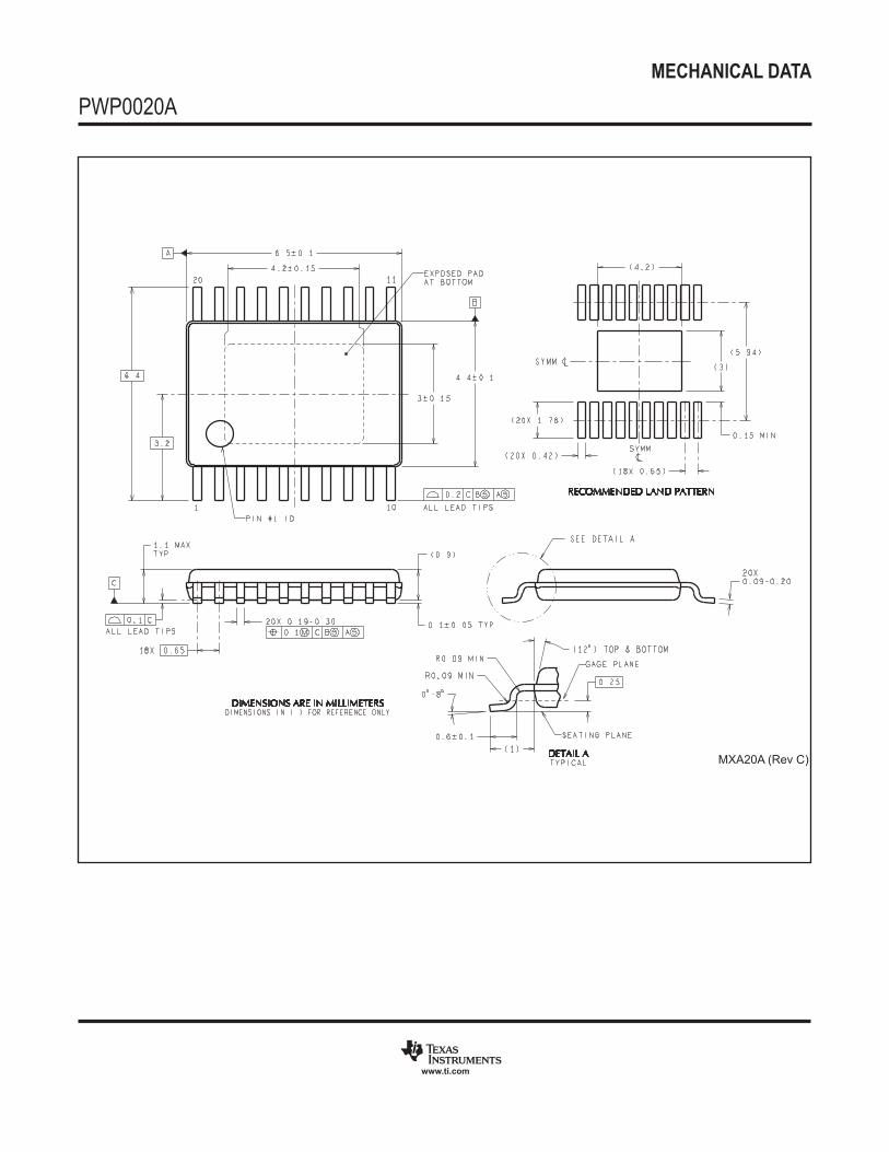
MECHANICAL DATA
PWP0020A
www.ti.com
MXA20A (Rev C)
IMPORTANT NOTICE
Texas Instruments Incorporated (TI) reserves the right to make corrections, enhancements, improvements and other changes to itssemiconductor products and services per JESD46, latest issue, and to discontinue any product or service per JESD48, latest issue. Buyersshould obtain the latest relevant information before placing orders and should verify that such information is current and complete.TI’s published terms of sale for semiconductor products (http://www.ti.com/sc/docs/stdterms.htm) apply to the sale of packaged integratedcircuit products that TI has qualified and released to market. Additional terms may apply to the use or sale of other types of TI products andservices.Reproduction of significant portions of TI information in TI data sheets is permissible only if reproduction is without alteration and isaccompanied by all associated warranties, conditions, limitations, and notices. TI is not responsible or liable for such reproduceddocumentation. Information of third parties may be subject to additional restrictions. Resale of TI products or services with statementsdifferent from or beyond the parameters stated by TI for that product or service voids all express and any implied warranties for theassociated TI product or service and is an unfair and deceptive business practice. TI is not responsible or liable for any such statements.Buyers and others who are developing systems that incorporate TI products (collectively, “Designers”) understand and agree that Designersremain responsible for using their independent analysis, evaluation and judgment in designing their applications and that Designers havefull and exclusive responsibility to assure the safety of Designers' applications and compliance of their applications (and of all TI productsused in or for Designers’ applications) with all applicable regulations, laws and other applicable requirements. Designer represents that, withrespect to their applications, Designer has all the necessary expertise to create and implement safeguards that (1) anticipate dangerousconsequences of failures, (2) monitor failures and their consequences, and (3) lessen the likelihood of failures that might cause harm andtake appropriate actions. Designer agrees that prior to using or distributing any applications that include TI products, Designer willthoroughly test such applications and the functionality of such TI products as used in such applications.TI’s provision of technical, application or other design advice, quality characterization, reliability data or other services or information,including, but not limited to, reference designs and materials relating to evaluation modules, (collectively, “TI Resources”) are intended toassist designers who are developing applications that incorporate TI products; by downloading, accessing or using TI Resources in anyway, Designer (individually or, if Designer is acting on behalf of a company, Designer’s company) agrees to use any particular TI Resourcesolely for this purpose and subject to the terms of this Notice.TI’s provision of TI Resources does not expand or otherwise alter TI’s applicable published warranties or warranty disclaimers for TIproducts, and no additional obligations or liabilities arise from TI providing such TI Resources. TI reserves the right to make corrections,enhancements, improvements and other changes to its TI Resources. TI has not conducted any testing other than that specificallydescribed in the published documentation for a particular TI Resource.Designer is authorized to use, copy and modify any individual TI Resource only in connection with the development of applications thatinclude the TI product(s) identified in such TI Resource. NO OTHER LICENSE, EXPRESS OR IMPLIED, BY ESTOPPEL OR OTHERWISETO ANY OTHER TI INTELLECTUAL PROPERTY RIGHT, AND NO LICENSE TO ANY TECHNOLOGY OR INTELLECTUAL PROPERTYRIGHT OF TI OR ANY THIRD PARTY IS GRANTED HEREIN, including but not limited to any patent right, copyright, mask work right, orother intellectual property right relating to any combination, machine, or process in which TI products or services are used. Informationregarding or referencing third-party products or services does not constitute a license to use such products or services, or a warranty orendorsement thereof. Use of TI Resources may require a license from a third party under the patents or other intellectual property of thethird party, or a license from TI under the patents or other intellectual property of TI.TI RESOURCES ARE PROVIDED “AS IS” AND WITH ALL FAULTS. TI DISCLAIMS ALL OTHER WARRANTIES ORREPRESENTATIONS, EXPRESS OR IMPLIED, REGARDING RESOURCES OR USE THEREOF, INCLUDING BUT NOT LIMITED TOACCURACY OR COMPLETENESS, TITLE, ANY EPIDEMIC FAILURE WARRANTY AND ANY IMPLIED WARRANTIES OFMERCHANTABILITY, FITNESS FOR A PARTICULAR PURPOSE, AND NON-INFRINGEMENT OF ANY THIRD PARTY INTELLECTUALPROPERTY RIGHTS. TI SHALL NOT BE LIABLE FOR AND SHALL NOT DEFEND OR INDEMNIFY DESIGNER AGAINST ANY CLAIM,INCLUDING BUT NOT LIMITED TO ANY INFRINGEMENT CLAIM THAT RELATES TO OR IS BASED ON ANY COMBINATION OFPRODUCTS EVEN IF DESCRIBED IN TI RESOURCES OR OTHERWISE. IN NO EVENT SHALL TI BE LIABLE FOR ANY ACTUAL,DIRECT, SPECIAL, COLLATERAL, INDIRECT, PUNITIVE, INCIDENTAL, CONSEQUENTIAL OR EXEMPLARY DAMAGES INCONNECTION WITH OR ARISING OUT OF TI RESOURCES OR USE THEREOF, AND REGARDLESS OF WHETHER TI HAS BEENADVISED OF THE POSSIBILITY OF SUCH DAMAGES.Unless TI has explicitly designated an individual product as meeting the requirements of a particular industry standard (e.g., ISO/TS 16949and ISO 26262), TI is not responsible for any failure to meet such industry standard requirements.Where TI specifically promotes products as facilitating functional safety or as compliant with industry functional safety standards, suchproducts are intended to help enable customers to design and create their own applications that meet applicable functional safety standardsand requirements. Using products in an application does not by itself establish any safety features in the application. Designers mustensure compliance with safety-related requirements and standards applicable to their applications. Designer may not use any TI products inlife-critical medical equipment unless authorized officers of the parties have executed a special contract specifically governing such use.Life-critical medical equipment is medical equipment where failure of such equipment would cause serious bodily injury or death (e.g., lifesupport, pacemakers, defibrillators, heart pumps, neurostimulators, and implantables). Such equipment includes, without limitation, allmedical devices identified by the U.S. Food and Drug Administration as Class III devices and equivalent classifications outside the U.S.TI may expressly designate certain products as completing a particular qualification (e.g., Q100, Military Grade, or Enhanced Product).Designers agree that it has the necessary expertise to select the product with the appropriate qualification designation for their applicationsand that proper product selection is at Designers’ own risk. Designers are solely responsible for compliance with all legal and regulatoryrequirements in connection with such selection.Designer will fully indemnify TI and its representatives against any damages, costs, losses, and/or liabilities arising out of Designer’s non-compliance with the terms and provisions of this Notice.
Mailing Address: Texas Instruments, Post Office Box 655303, Dallas, Texas 75265Copyright © 2018, Texas Instruments Incorporated